Submitted:
06 March 2026
Posted:
09 March 2026
You are already at the latest version
Abstract
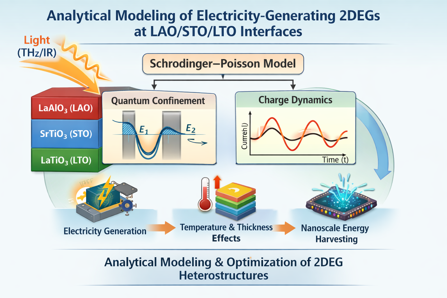
Two-dimensional electron gases (2DEGs) in complex oxide heterostructures provide a powerful platform for enabling nanoscale energy-conversion mechanisms. In this work, we investigate LaAlO₃/SrTiO₃/LaTiO₃ (LAO/STO/LTO) interfaces as an engi-neered architecture for electricity generation, exploiting the combined effects of LAO-induced polar discontinuity, STO’s high-κ dielectric response, and LTO-driven electronic reconstruction. This trilayer system generates a strongly confined interfacial 2DEG with sheet densities in the 1013–1014 cm−2 range, enabling strong interaction with external electromagnetic fields and efficient charge displacement. To quantitatively capture the physics governing 2DEG formation and energy extraction, we develop a self-consistent analytical model solving the Schrödinger–Poisson equations. The SP module resolves quantum confinement, band bending, and carrier distribution at the LAO/STO/LTO interface, while the analytical engine models electromagnetic excitation (sheet charge density ns), field enhancement, and dynamic charge response across the heterostructure. This approach enables simultaneous evaluation of subband structure, interfacial potential, plasma-resonance behavior, and field-induced current genera-tion. Simulation results demonstrate that the asymmetric LAO/STO/LTO stack pro-duces a deep quantum well on the STO side, promoting strong 2DEG confinement and enhanced sensitivity to THz–IR excitation; under illumination the 2DEG exhibits res-onant carrier modulation, enhanced drift displacement, and energy-transfer pathways conducive to electricity generation. We additionally incorporate temperature depend-ence into the model and find monotonic increases in sheet charge density and conduc-tivity with temperature (measured at zero bias for 10 nm films), with LTO showing metallic-like, strongly temperature-dependent transport, STO exhibiting modest ther-mally activated behavior, and LAO remaining effectively insulating but most sensitive in relative terms—effects that alter subband occupancy, screening, and resonance con-ditions. The model clarifies how layer thickness, dielectric contrast, interface polariza-tion, and temperature jointly govern energy-conversion efficiency. Overall, the vali-dated Schrödinger–Poisson framework provides a predictive tool for optimizing oxide 2DEG power-generating structures and positions LAO/STO/LTO heterointerfaces as promising candidates for tunable, nanoscale energy-harvesting devices.
Keywords:
2DEG
; LAO/STO/LTO interfaces
; Schrödinger–Poisson modeling
; analytical model
; oxide heterostructures
; electricity generation
; polar discontinuity
; quantum confinement
; perovskite interfaces
1. Introduction
Two-dimensional electron gases (2DEGs) formed at oxide heterointerfaces have emerged as a versatile platform for next-generation nanoelectronic and energy-conversion technologies [1]. Unlike conventional semiconductor 2DEGs, complex oxides such as LaAlO₃/SrTiO₃/LaTiO₃ (LAO/STO/LTO) exhibit rich interfacial physics driven by polar discontinuities, strong electronic correlations, and large dielectric responses [2]. These effects produce high-density, quantum-confined electron liquids capable of supporting tunable conduction, nonlinear optical activity, and strong coupling to external electromagnetic fields [3]. Recent studies have shown that correlated oxide 2DEGs can undergo electronic reconstruction, metal–insulator transitions, and even superconductivity, positioning them as candidates for electrically and optically driven functional devices [4,5]. For energy-harvesting applications, oxide 2DEGs offer distinct advantages: strong charge confinement enhances field-induced carrier dynamics; high dielectric screening in STO reduces scattering; and built-in polar fields provide natural asymmetry for charge separation [6]. However, capturing these coupled electromagnetic and quantum-electrostatic processes requires a multiphysics modeling framework that resolves both quantum confinement and dynamic field–carrier interactions.
In this work, we develop a Schrödinger–Poisson self-consistent analytical model to investigate electricity generation mechanisms in 2DEGs formed at LAO/STO/LTO interfaces. By integrating quantum electrostatics with time-dependent electromagnetic excitation, we quantify subband occupation, interfacial potential profiles, plasma resonance behavior, and field-induced charge displacement. This combined approach enables predictive insight into how structural asymmetry, dielectric contrast, and polar layering govern energy-conversion efficiency in oxide heterostructures.
1.1. Families of 2DEG Materials for Electronic and Optoelectronic Devices
Two-dimensional electron gases (2DEGs) have been realized in a wide variety of material systems, each with distinct electrical and optical figures of merit [7]:
- III–V semiconductor heterostructures (e.g. AlGaAs/GaAs, InAs QWs) [8]
- Wide bandgap III nitrides (AlGaN/GaN, GaN/AlN) [9]
- Complex oxides based on SrTiO₃ (STO) or ZnO (e.g. LaAlO₃/SrTiO₃, LaTiO₃/SrTiO₃, MgZnO/ZnO) [10]
- Van der Waals 2D materials (graphene, MoS₂ and other transition metal dichalcogenides) [11]
From a device engineering viewpoint, relevant performance metrics include:
- Sheet carrier density ns,
- Mobility µ and breakdown field,
- Tunability via electric field, strain or illumination, and
- Optical response from THz up to UV [12].
The goal of this work is not to maximize a single metric (e.g. mobility) but to identify a platform that combines electrical tunability, rich quantum phases, strong optical response and compatible CMOS integration. Within that multi criteria framework, the LaTiO₃/SrTiO₃ (LTO/STO) interface emerges as particularly attractive, as discussed below [13].
1.2. Conventional III-V- Semiconductors 2DEGs
The earliest and still most mature 2DEG systems are modulation doped AlGaAs/GaAs and related III–V heterostructures [14]. Spatial separation between donors in AlGaAs and electrons in the GaAs quantum well strongly suppresses impurity scattering and enabled record low temperature mobilities µ > 3.5×10⁷ cm²/V·s at densities around 3×1011 cm-2 [15]. These structures underpin much of our understanding of quantum Hall physics and ballistic transport. Optically, high purity GaAs QWs exhibit sub meV photoluminescence (PL) linewidths and well resolved excitonic features, making them excellent testbeds for cavity QED, lasers and nonlinear optics. Pelucchi et al. demonstrated samples with simultaneously >10⁶ cm²/V·s mobility and sub meV PL linewidth, which is often taken as a benchmark of optical electrical quality in III–V 2DEGs [16]. However, GaAs-based 2DEGs suffer from relatively small band gaps and low breakdown fields, limiting high-power operation and robustness under strong electric fields. Their optical response is mostly in the near IR, and they lack the strong correlation effects, giant dielectric constant and multi-phase behavior (superconductivity, ferromagnetism) available in oxides. Moreover, integrating high mobility GaAs 2DEGs directly on Si remains challenging despite progress in GaAs on Si epitaxy [17]. For these reasons, while III–V 2DEGs are unrivalled for low temperature basic physics, they are not ideal for oxide electronics oriented, multifunctional 2DEG studies like the present one [18].
1.3. 2DEGs in Wide-Bandgap III-Nitrides
In AlGaN/GaN and related nitride heterostructures, 2DEGs are formed by spontaneous and piezoelectric polarization rather than modulation doping [19]. Ambacher and coworkers showed that the large polarization discontinuity at the AlGaN/GaN interface induces fixed sheet charge and 2DEG densities up to ~2×1013 cm-2 without intentional dopants [20]. Typical room temperature mobilities range from 1000–2000 cm²/V.s, enabling high frequency and high-power HEMTs with breakdown voltages in the hundreds of volts and switching frequencies in the GHz regime [21]. Optically, GaN and its alloys have wide bandgaps (~3.4 eV for GaN, larger for AlGaN) and strong optical transitions in the UV. 2DEG-based nitride structures have been used for high-gain photodetectors, where the confined channel provides internal gain and high responsivity [22]. However, compared with oxides, nitride 2DEGs typically do not show gate tunable superconductivity or strong correlation effects, and their dielectric constant is modest compared to STO, which limits the range of electric field control [23].
1.4. Oxide 2DEGs
Complex oxide interfaces provide a qualitatively different route to 2DEGs, driven by polar discontinuities, orbital reconstructions, and oxygen vacancy chemistry [24]. In oxide systems, simulation strategies range from Poisson– Schrödinger solvers with effective-mass approximations to full density-functional theory (DFT) including correlation effects. Because correlation and lattice instabilities strongly influence transport in complex oxides, SP models are often calibrated against, or supplemented by, DFT-based calculations of band structures and interface states [25]. Complex oxide interfaces provide a qualitatively different route to 2DEGs driven by polar discontinuities, orbital reconstructions, and oxygen-vacancy chemistry [26].
1.4.1. LAO/STO Structure
The LaAlO₃/SrTiO₃ (LAO/STO) interface is the prototypical oxide 2DEG system [27]. Ohtomo and Hwang discovered that when the LAO overlayer exceeds a critical thickness, a high mobility electron gas forms at the interface between two insulating oxides [28]. Subsequent work reported superconductivity, magnetism and large Rashba spin–orbit coupling in this 2DEG [29,30]. A landmark discovery by Ohtomo and Hwang showed that a high mobility electron gas can form at the interface between two band-insulating perovskites, LaAlO₃ and SrTiO₃ (LAO/STO), when the LAO layer exceeds a critical thickness. This result established polar oxide heterostructures as tunable 2DEG platforms [28]. Subsequent work by Salluzzo et al. demonstrated that the LAO/STO 2DEG is associated with an orbital reconstruction of Ti 3d states at the interface, as revealed by X-ray absorption spectroscopy, providing microscopic insight into how electronic structure drives interfacial conduction. Work by Salluzzo et al demonstrated the LAO/STO 2DEG associated with an orbital reconstruction of Ti 3d state at the interface as revealed by X-ray absorption spectroscopy, providing microscopic insight into how electronic structure drives interfacial conduction [31,32]. Bark et al. showed that epitaxial strain in STO can be used to tailor the carrier density and mobility of the LAO/STO 2DEG, highlighting the importance of mechanical boundary conditions in oxide 2DEG engineering [33]. Trier et al. reviewed electron mobility in oxide heterostructures more broadly, demonstrating that mobilities can rival those of traditional semiconductors when defect densities are controlled and emphasizing that good agreement between experiment and simulation requires accurate treatment of dielectric screening, electron–phonon coupling, and localization effects [34]. Electrically, LAO/STO supports sheet carrier densities of ~1013 cm-2 with low temperature mobilities typically in the 10³–10⁴ cm²/V·s range, depending on growth conditions and oxygen vacancy content [35]. Optically, STO has a large, tunable dielectric constant and strong infrared phonon modes, and LAO/STO structures show THz and infrared resonances, surface phonon polaritons and tunable THz emission. These properties make LAO/STO a powerful platform for THz photonics and nonlinear optics [36].
1.4.2. MgZnO/ZnO Structure
Beyond LAO/STO, 2DEGs have been realized and exploited in MgZnO/ZnO heterostructures with extremely high mobility. Falson et al. reported molecular beam epitaxy (MBE) - grown MgZnO/ZnO with µ > 1×10⁶ cm²/V·s at low temperature, comparable to the best III–V systems, showing that control of growth conditions and defect management can produce oxide 2DEG of exceptionally high quality [37]. Kozuka et al. reported quantum Hall quality 2DEGs with mobility ~3×10⁵ cm²/V·s, revealing the role of oxygen vacancies, Polar distortions and strong dielectric nonlinearity significantly affect the quality of 2DEGs [38]. Optically, ZnO has a direct bandgap of ~3.3 eV and strong excitonic effects, and MgZnO/ZnO 2DEG structures have been used to realize high-performance UV photodetectors with large responsivity and UV/visible rejection ratios enhanced by the presence of the 2DEG channel. These systems are excellent for UV optoelectronics and quantum Hall physics, but they do not naturally couple to a Mott-insulating layer or exhibit gate-tunable superconductivity [39].
1.5. Two-Dimensional Materials
1.5.1. Graphene
In graphene, the conduction electrons form a truly two-dimensional Dirac electron gas [40]. Suspended graphene devices have demonstrated mobilities ~2×10⁵ cm²/V.s at low temperature (4-20 K), surpassing any conventional semiconductor [41]. Graphene has a gapless Dirac spectrum and broadband optical absorption (~2.3% per layer) from visible to mid IR, enabling strong plasmonic and THz responses [42]. However, the absence of a bandgap makes it challenging to obtain high on/off ratios for logic, and integration of crystalline oxide overlayers with high structural quality is nontrivial [43].
1.5.2. MoS2 Material
Monolayer MoS₂ and other TMDs provide atomically thin semiconducting channels with direct bandgaps in the visible (1.8–2.0 eV), strong excitonic absorption and valley selective optical selection rules [44]. Room temperature mobilities, however, are typically tens to a few hundred cm²/V·s, far below what is available in III–V or oxide 2DEGs, although strain engineering and dielectric engineering can enhance mobility [45]. Thus, while van der Waals 2D materials excel in scalability and optical functionality, they do not yet combine high mobility, strong correlation and oxide compatible processing in the way LAO/STO does. The Representative 2DEG material systems and key properties) electrical and optical) are illustrated in Table 1.
Representative ranges compiled from Refs. for GaAs/AlGaAs, AlGaN/GaN, MgZnO/ZnO, β-(Al,Ga), LAO/STO, LTO/STO, graphene and MoS.
2. Materials Used
In this work we will use three materials as given below:
- (a)
- LaTiO₃ (LTO)
LTO is an orthorhombically distorted perovskite (ABO₃) with a pseudocubic lattice parameter ≈3.96 Å, close to STO, so it can grow coherently and form sharp interfaces [47]. Electronically, it is a 3d¹ Mott–Hubbard insulator with a very small correlation gap (~0.1–0.2 eV), so its Ti 3d states lie close to the Fermi level and can easily donate electrons to neighboring STO [48]. It is polar along (001) with (LaO)⁺/(TiO₂)⁻ layers, has a moderate dielectric constant (εᵣ ≈20–40), and shows G type antiferromagnetism (Tᴺ ~140 K) [49]. This combination of polar layering, small gaps, and reasonable permittivity makes LTO an efficient reservoir layer that can drive 2DEG formation on the STO side in LTO/STO heterostructures [50].
- (b)
- SrTiO₃ (STO)
STO is a cubic perovskite (a = 3.905 Å) and a wide band gap band insulator with an indirect gap ≈ 3.2–3.3 eV [51]. Its most important feature for 2DEG physics is its enormous, strongly temperature dependent dielectric constant (εᵣ ≈ 300 at room temperature and >10³ at low temperature), which provides excellent screening of Coulomb disorder while still allowing strong built in fields at interfaces [52]. STO is non polar along (001) with (SrO)⁰/(TiO₂)⁰ layers and is non magnetic in bulk. In LAO/STO and LTO/STO, the 2DEG actually lives in the STO side: its high κ response and suitable Ti 3d conduction band form the quantum well that confines the interfacial electrons [53].
- (c)
- LaAlO₃ (LAO)
LAO is a rhombohedrally distorted perovskite, often treated as pseudo cubic with a ≈3.79 Å, so LAO films on STO are under tensile strain but still epitaxial [54]. It is a wide band gap insulator (E₉ ≈5.5–5.6 eV) with a moderate dielectric constant (εᵣ ≈20–25). Crucially, along (001) LAO is polar, consisting of alternating (LaO)⁺ and (AlO₂)⁻ planes; when this polar stack is grown on non-polar STO, a polar discontinuity appears [55]. Above a critical thickness (~3–4 unit cells), this drives electronic reconstruction and transfer of electrons into the STO conduction band, creating the LAO/STO 2DEG [56]. Thus, LAO’s polar layering, wide gap (large band offsets), and decent κ make it an ideal polar overlayer to induce and control a 2DEG at the LAO/STO interface [57].
2.1. Electrical and Optical Properties of the LTO/STO 2DEG
At the LaTiO₃/SrTiO₃ (LTO/STO) interface, a 2DEG forms between a Mott insulator (LTO, Ti³⁺, d¹) and a band insulator (STO, Ti⁴⁺, d⁰) [58]. Biscaras et al. demonstrated that this interfacial 2DEG undergoes a two-dimensional superconducting transition at Tc ≈ 300 K, with a superconducting layer thickness of ~12 nm, located mostly on the STO side [59]. Hall and magneto transport measurements indicate sheet densities ns∼1013 - 1014 cm-2 and coexistence of two carrier types: a majority of low mobility carriers and a minority of high mobility carriers that are crucial for superconductivity [60].
More recently, THz time domain spectroscopy on STO/LTO/STO heterostructures grown on Si(001) has quantified the dynamic transport properties: Bhattacharya and coworkers report carrier densities on the order of 1012 cm-2 and mobilities around 10³ cm²/V·s in the THz regime, confirming a delocalized 2D electron liquid relevant for high frequency electronics and detectors [61].
Electrically, LTO/STO also shows:
- Metal–insulator transitions as a function of LTO thickness and oxygen stoichiometry, especially in structures integrated on Si (100) [62].
- Competing conduction mechanisms, where intrinsic electronic reconstruction, oxygen vacancies in STO and La/Sr intermixing all contribute to the observed 2DEG, making it a rich system for studying defect-controlled transport [63].
- Remote doping of Si (001): Jin et al. showed that an LTO/STO 2DEG can be used as an oxide remote dopant to induce a second 2DEG directly inside a silicon substrate, demonstrating electronic coupling between oxide and Si channels [64].
Optically, STO based interfaces are characterized by:
- Very large, temperature dependent dielectric constants (ε ≫ 300 at low T), which place the plasma frequency of the 2DEG, and phonon coupled plasmons in the THz range [65].
- Strong infrared and THz absorption associated with Drude carriers and polar phonons; LTO/STO specifically exhibits a THz Drude response whose spectral weight shifts with temperature and carrier density [66].
- Sensitivity to nonlinear optical probes: surface specific nonlinear optics and ultrafast spectroscopy have been used to resolve structural and electronic dynamics at perovskite oxide interfaces, indicating that STO based 2DEGs couple strongly to light over a broad spectral range [67].
In summary, LTO/STO offers a 2DEG with moderate but sufficient mobility (~10²–10³ cm²/V·s), high sheet density (~10¹³–10¹⁴ cm⁻²), gate tunable superconductivity, metal–insulator transitions, and strong THz/infrared optical response, all hosted in a platform that can be integrated on silicon [68]. Comparing the material families above, we can now articulate why LTO/STO is the “best” choice for the goals of this study, which are: to simulate and engineer a 2DEG for electrical and optoelectronic applications in a complex oxide system, using analytical model [69].
- 1.
- Multifunctionality (electrical + quantum phases).
- GaAs and MgZnO/ZnO provide record mobility but do not naturally host gate tunable superconductivity and Mott physics [70].
- LAO/STO is superconducting but involves only band insulators; LTO/STO additionally couples the 2DEG to a Mott insulator, enabling studies of correlated charge transfer [71].
For a simulation paper centered on the interplay between 2DEG formation, correlations and transport, LTO/STO therefore offers the richest physics [72].
- 2.
- Strong electrical tunability with realistic voltages.
The enormous dielectric constant of STO and the intermediate carrier density of the LTO/STO 2DEG mean that gate voltages of a few tens of volts can drive large changes in sheet density, induce or suppress superconductivity, and even trigger metal–insulator transitions. This is ideal for validating a self-consistent Schrödinger–Poisson–analytical model across a wide parameter space [73].
- 3.
- Broadband optical response (THz to visible).
LTO/STO interfaces show Drude like THz conductivity, infrared phonon polaritonic features and potential near IR/visible optical transitions inherited from the Ti 3d manifold and STO band structure. This makes them promise for THz detectors, modulators, and optically driven devices, which align with interest in electrical applications that are also optically active [74].
- 4.
- Oxide–silicon integration.
Unlike many other complex oxides, LTO/STO can be grown directly on Si (100) via STO buffer layers, and both the 2DEG and the metal–insulator behavior has been demonstrated on silicon. Combined with remote doping of Si by the oxide 2DEG, this positions LTO/STO as one of the most CMOS relevant oxides 2DEG platforms [75].
- 5.
- Numerical tractability and relevance for analytical modeling.
The LTO/STO 2DEG is well confined (10–15 nm), quasi one dimensional in the confinement direction and reasonably described by effective mass models in STO, making it ideal for finite difference time domain Schrödinger solvers coupled to Poisson. At the same time, there is a rich experimental dataset (DC, Hall, THz, superconductivity) to calibrate and validate the simulations [76].
Taken together, these points justify the focus on LTO/STO in this work: among the various 2DEG material platforms, it offers the best compromise between electrical performance, optical/THz activity, rich correlated phases, and silicon compatibility. It is therefore an ideal testbed for the analytical model, self-consistent simulation and modeling of 2DEG formation.
2.2. Electrical and Optical Properties of the LAO/STO 2DEG
At the LaAlO₃/SrTiO₃ (LAO/STO) interface, a 2DEG forms between two wide gap band insulators: polar LaAlO₃ (LAO) and non-polar SrTiO₃ (STO) [77]. When the LAO overlayer exceeds a critical thickness of ≈3–4-unit cells, the polar (LaO)⁺/(AlO₂)⁻ stacking drives an “electronic reconstruction” in which electrons are transferred into Ti 3d states on the STO side, creating a conducting interfacial layer that is metallic at low temperature [78]. This LAO/STO 2DEG is now the archetypal oxide interface system, combining high carrier density, strong gate tunability, and emergent quantum phases [79]. Transport and magnetotransport studies show that the LAO/STO 2DEG exhibits two-dimensional superconductivity with an onset critical temperature Tc ∼200 - 300 K, and a superconducting thickness of order 10–20 nm, again largely confined to the STO side of the interface [80]. Hall measurements typically find sheet carrier densities ns ~ 1013 cm-2 (with values up to the high 10¹³ cm⁻² range depending on growth and oxygen stoichiometry), together with multi band conduction: a majority of relatively low mobility carriers and a minority of high mobility carriers that are particularly important for superconductivity and quantum transport [81]. Low temperature mobilities in optimized samples can reach 103 - 104 cm2.V-1.s-1, while room temperature values are typically in the few–tens of cm²/V·s range [82].
Electrically, LAO/STO also shows:
- Gate tunable superconductivity and metal–insulator transitions: both back gating through STO and top gating through metallic electrodes can continuously tune the 2DEG carrier density, driving the system across a superconducting dome in the TC (ns) phase diagram and into insulating or weakly localized regimes [83].
- Strong Rashba spin–orbit coupling and exotic transport: the broken inversion symmetry at the interface produces sizeable Rashba coupling, leading to tunable spin–orbit fields and giant nonreciprocal charge transport as a function of gate voltage [84].
- Coexistence of ferromagnetism and superconductivity: scanning probe and magneto transport experiments reveal nanoscale ferromagnetism coexisting with the superconducting 2DEG, providing a platform to study interplay between these usually antagonistic orders in two dimensions [85].
Optically, LAO/STO and related STO based interfaces are characterized by:
- Large, temperature dependent dielectric response of the STO host (ε ≫ 300 at low temperature), pushing the 2DEG plasma frequencies and phonon–plasmon coupled modes into the THz range and making the system highly responsive in the far infrared [86].
- Strong Drude like THz and infrared absorption arising from in plane free carriers coupled to polar phonons; detailed modeling of the LAO/STO optical conductivity shows a low frequency Drude contribution plus phonon polaritonic features sensitive to carrier density and confinement [87].
- Sensitivity to nonlinear optical probes: second harmonic generation (SHG) and surface specific THz nonlinear spectroscopy have been used to directly probe interfacial symmetry breaking, charge density, and low frequency resonances of the 2DEG, highlighting strong coupling between lattice, charge, and light at the LAO/STO interface [89].
In summary, LAO/STO provides a high density 2DEG with moderate to high mobility, gate tunable superconductivity, spin–orbit driven phenomena, and a pronounced THz/infrared and nonlinear optical response, all realized in a perovskite platform that is now one of the most thoroughly characterized oxide interfaces in the literature [89]. Comparing the different 2DEG material families, LAO/STO stands out as the benchmark complex oxide interface for our goals: to simulate and engineer a 2DEG for electrical and optoelectronic applications using a quantitative analytical model using Schrödinger–Poisson equations [90].
- Strong electrical tunability with realistic voltages. The enormous dielectric constant of STO and the intermediate carrier density of the LAO/STO 2DEG mean that modest back or top gate voltages (tens of volts, or less with high κ gates) can continuously tune the sheet carrier density over a broad yet sub-order-of-magnitude range drive metal–insulator or superconductor–insulator transitions, and tune spin–orbit and nonreciprocal responses. This makes LAO/STO ideal for validating a self-consistent Schrödinger–Poisson model over a broad parameter space of carrier density and confining potential [93].
- Broadband optical and THz response. The combination of Drude carriers, polar phonons, and soft-mode dielectric behavior in STO produces strong THz and infrared signatures, while SHG and other nonlinear probes are sensitive to interfacial symmetry breaking and 2DEG density. These broadband optical observables provide additional experimental benchmarks (beyond DC and Hall data) to which our simulations can be compared and highlight the relevance of LAO/STO for THz detectors, modulators, and optically driven oxide devices [94].
- Oxide–silicon integration. LAO/STO heterostructures can be integrated with silicon using STO buffer layers on Si (001), followed by epitaxial growth of LAO, enabling 2DEG based oxide functionalities to be combined with CMOS compatible platforms. This creates a realistic technological context for the simulated devices, especially for on chip power and sensing applications [95].
- Numerical tractability and relevance for analytical modeling. The LAO/STO 2DEG is confined within ~10–20 nm on the STO side, is effectively two dimensional in the confinement direction, and is reasonably described by an effective mass picture in the Ti 3d conduction band, making it well suited to finite difference Schrödinger solvers coupled to Poisson. At the same time, a large experimental data set (DC transport, Hall, superconducting phase diagrams, optical and nonlinear optical measurements) is available to calibrate and validate the simulations [96].
Despite substantial progress in modeling 2DEG formation in III-nitride and oxide heterostructures, important limitations remain. Current studies are largely material-specific, with limited integration of quantum, electrostatic, and transport simulations within unified frameworks [97,98]. In addition, strain, polarization, and interface effects are not consistently treated, and transferable compact models suitable for emerging heterostructures and circuit-level applications are still lacking [99,100].The present work addresses the identified research gaps by developing a unified multiphysics simulation framework for 2DEG formation and transport that integrates Schrödinger–Poisson calculations with device-level drift–diffusion modeling while consistently incorporating strain, polarization, and interface trap effects [101,102]. The framework further enables the derivation of analytical or semi-analytical expressions for 2DEG density and effective mobility suitable for compact circuit models [103]. Through benchmarking across III-nitride and oxide heterostructures, the study aims to establish transferable design guidelines for 2DEG-based electronic devices beyond material-specific optimization.
3. Proposed Structure and Analytical Modeling
The proposed structure is illustrated in Figure 1 below. The figure illustrates the formation of a two-dimensional electron gas (2DEG) in a tri-layer oxide heterostructure composed of LAO, STO, and LTO. In this configuration, the wide-bandgap insulating LAO layer is deposited on STO, while the Mott-insulating LTO layer lies beneath the STO, creating asymmetric electronic boundary conditions across the interfaces. Due to band alignment, charge transfer, and strong electronic reconstruction, the conduction band of STO bends downward near the STO/LTO interface, leading to the accumulation of electrons confined within a narrow potential well. These electrons are free to move laterally along the interface but are quantum-confined in the vertical direction, giving rise to a high-mobility 2DEG. The figure highlights this confined electron layer at the STO–LTO interface, emphasizing the role of polar discontinuity, band bending, and interfacial charge redistribution in stabilizing the 2DEG within complex oxide heterostructures.
The energy band diagram of the LAO, STO, and LTO heterostructure illustrates how band alignment and interfacial effects lead to the formation of a two-dimensional electron gas (2DEG). LAO, with its wide band gap, exhibits a high conduction band minimum, while STO has a smaller band gap with its conduction band positioned lower in energy. LTO, being a Mott insulator, contributes occupied Ti 3d states close to the Fermi level. At the interfaces, electrostatic potential buildup and electronic reconstruction cause significant band bending within the STO layer, pulling its conduction band below the Fermi level near the STO/LTO interface. This creates a quantum well that confines electrons in the out-of-plane direction while allowing free in-plane transport. The resulting accumulation of electrons at the interface forms the 2DEG, as depicted in the band diagram, highlighting the crucial role of band offsets, charge transfer, and interfacial polarization in governing the electronic properties of the heterostructure, as given in Figure 2.
The main key factor in the performance of 2DEG device is the sheet charge density (ns), which can be calculated using a self-consistent Schrödinger–Poisson equations [104]. By neglecting the higher states, the ns can be calculated using Equation (1):
where:
is the thermal voltage and , is the Fermi-Dirac distribution function, and is the effective mass of electrons.
For a completely ionized 2DEG layer, the sheet charge density can be calculated using Equation (2):
where: and are the permittivity of the first and second material used in the 2DEG respectively, and are the material thickness, is the biased voltage applied to the gate, is the flat-band voltage of the structure (4.42 V), and the is the fermi energy level in volt.
The model parameters are given in the table below for the three used structures LTO, STO and LAO (Table 2).
Electrical Conductivity
Electrical conductivity in a 2DEG system refers to how efficiently the electron gas layer conducts electricity. It is significantly influenced by electron mobility and the density of states within this two-dimensional layer [105]. The electrical conductivity (σ) can be calculated using Equation (3):
where: is the relaxation time ( [106], [107], and [108]).
4. Results and Analysis
This section presents a comprehensive analysis of the electrical properties of two-dimensional electron gases (2DEGs) at LAO/STO/LTO interfaces, as derived from the self-consistent analytical model employing coupled Schrödinger–Poisson equations. The core objective is to quantify the behavior of sheet charge density and electrical conductivity under varying structural parameters and external influences, thereby shedding light on their potential for nanoscale energy conversion.
4.1. Sheet Charge Density Characteristics
The sheet charge density (ns) is a paramount indicator of a 2DEG's electrical performance, representing the concentration of highly mobile charge carriers confined at the interface. Its magnitude directly dictates the device's ability to conduct current and respond to external fields.
Figure 3 vividly illustrates the critical role of material choice and layer thickness in 2DEG formation. For all materials investigated, a general trend of decreasing sheet charge density with increasing 2DEG thickness is observed. This behavior is fundamentally linked to quantum confinement; in thinner layers, electrons are more tightly confined, leading to higher spatial concentration and thus greater (ns). Conversely, as the thickness increases, the confinement weakens, allowing for a more dispersed electron distribution and reduced (ns).
Among the three structures, the LTO layer consistently yields the highest sheet charge density, achieving values in the 10¹⁶ cm⁻² range, particularly at thinner (e.g., 4 nm) 2DEG thicknesses. This superior performance of LTO can be attributed to its inherent properties as a Mott-Hubbard insulator with a small correlation gap, facilitating effective electron donation to the neighboring STO layer and creating a robust charge reservoir. STO exhibits moderate () values, reflecting its high dielectric constant that aids electron confinement, while LAO demonstrates the lowest () across all thicknesses, suggesting its primary role as a polar overlayer for inducing the 2DEG rather than contributing significantly to its density. These distinctions underscore the design flexibility offered by each material in tailoring charge carrier concentration.
Figure 4 provides crucial insights into the electrical tunability of these oxide interfaces, a key requirement for active device applications. The plot clearly shows a positive and generally linear relationship between the applied gate voltage and the sheet charge density for all three materials at a fixed 2DEG thickness of 5 nm. This linearity confirms the effectiveness of external electric fields in modulating the carrier concentration within the 2DEG.
Once again, LTO-based interfaces exhibit the most significant tunability and the highest absolute sheet charge density values across the entire gate voltage range (from -1 V to 3 V). The steep slope of the LTO curve signifies its high sensitivity to external biasing, making it an excellent candidate for gate-tunable devices, such as field-effect transistors and modulators. STO shows a respectable, albeit lower, tunability, while LAO demonstrates the lowest (ns) values and minimal response to gate voltage variations. This disparity in tunability is directly influenced by the dielectric properties and interface charge dynamics of each material layer, with LTO offering the most dynamic control over its 2DEG.
Further analysis of the sheet charge density dependence on gate voltage for 10 nm (Figure 5) and 15 nm (Figure 6) thicknesses reveal consistent trends, albeit with quantitatively different values. At both 10 nm and 15 nm, all materials (LTO, STO, LAO) continue to exhibit a linear increase in sheet charge density with increasing gate voltage, confirming robust electrical tunability across varying thicknesses. However, a general reduction in the absolute sheet charge density values is observed for all materials as the thickness increases from 5 nm to 10 nm, and further to 15 nm. This reinforces the earlier observation from Figure 1: that stronger quantum confinement in thinner layers leads to higher carrier concentrations. Despite this reduction, LTO consistently maintains its position as the material with the highest sheet charge density and strongest tunability compared to STO and LAO at both 10 nm and 15 nm. The LAO layer, in particular, shows extremely low (ns) values at these greater thicknesses, suggesting its limited utility for high charge density applications beyond its role in inducing polar discontinuity. These consistent gate tunability trends across varying thicknesses underscore the potential for fine-tuning 2DEG properties for specific device requirements.
4.2. Electrical Conductivity Analysis
Electrical conductivity (σ) is a direct measure of a material's capacity to facilitate charge transport and is a critical figure of merit for energy-harvesting applications. As defined by Equation (3) where (n) is the sheet charge density, (e) is the elementary charge, (τ) is the electron relaxation time, and () is the effective electron mass. This equation highlights the direct dependence of conductivity on both the carrier concentration and the efficiency of carrier transport (relaxation time).
Table 3 provides a quantitative assessment of the electrical conductivity for LTO, STO, and LAO at various thicknesses (5 nm, 10 nm, and 15 nm).
The results overwhelmingly demonstrate LTO's exceptional electrical conductivity, which dramatically surpasses that of STO and LAO across all investigated thicknesses. At a 5 nm thickness, LTO exhibits a conductivity of 1903.10 S/cm, orders of magnitude higher than STO (2.52 S/cm) and LAO (0.05 S/cm). This remarkable difference is primarily driven by two factors: LTO's superior sheet charge density (as observed in Figure 1) and its significantly longer electron relaxation time (τ = 650 ns), which are several orders of magnitude greater than 0.99 ns and 0.07 ns respectively. A longer relaxation time implies fewer scattering events and more efficient transport.
Furthermore, a consistent decrease in electrical conductivity with increasing 2DEG thickness is observed for all materials. For LTO, conductivity drops from 1903.10 S/cm (5 nm) to 634.37 S/cm (15 nm). This trend directly correlates with the decrease in sheet charge density as confinement weakens in thicker layers, but it also suggests that increased thickness might introduce more scattering centers or reduce the overall mobility. The pronounced difference in conductivity among the materials, especially the outstanding performance of LTO, positions it as a highly promising candidate for efficient energy harvesting.
4.3. Temperature Effect
In Figure 7, the effect of temperature on the sheet charge density was calculated using Equation (1). Calculated at zero bias on 10 nm films, the sheet charge density for all three interfaces increases approximately linearly from 280–380 K; LTO displays the largest absolute carrier density, STO is intermediate, and LAO the lowest while exhibiting the greatest relative temperature dependence. This trend is indicative of thermally activated carrier injection or ionization with differing activation strengths and trap depths across the interfaces, which will affect subband occupancy and screening in the 2D electron gas and should be distinguished from mobility-driven conductivity changes via temperature-dependent Hall and spectroscopic measurements.
The temperature dependent conductivity data exhibit three distinctly different transport regimes (as illustrated in Table 4); LTO shows metallic highly conductive behavior (σ ≈ 862 → 130 S/cm from 280 →380 K) with a large positive temperature coefficient, STO displays low-to-moderate semiconducting conductivity (σ ≈ 1.12 → 1.77 S/cm) with a steady temperature rise, and LAO is effectively insulating in this range (σ ≈ 0.02 → 0.05 S/cm). The orders-of-magnitude differences indicate fundamentally different carrier densities and/or mobilities at the interfaces (LTO ≫ STO ≫ LAO). The monotonic increase of σ(T) is consistent with thermally activated carrier population and/or reduced localization with temperature; however, the large absolute conductivity of LTO suggests a high intrinsic carrier concentration or metallic channel rather than simple thermal activation. To identify the dominant mechanism and separate carrier density from mobility effects, perform temperature-dependent Hall measurements, fit σ(T) or n(T) to activation models to extract activation energies, and obtain mobility µ(T) to assess scattering mechanisms (phonon vs impurity/defect scattering).
5. Conclusions
In this work, a self-consistent analytical framework based on coupled Schrödinger–Poisson equations were developed to investigate two-dimensional electron gas (2DEG) formation and transport in LAO/STO/LTO oxide heterostructures for nanoscale electrical and energy-conversion applications. The model integrates quantum confinement and electrostatic interactions within a unified multiphysics approach, enabling systematic evaluation of sheet carrier density and electrical conductivity under variations in layer thickness, gate bias, and temperature. Although material parameters were defined for individual layers, the simulations were performed across the complete heterostructure, allowing interfacial band alignment, polarization discontinuity, and charge transfer to be treated self-consistently.
The results confirm that the electrical behavior originates from interface-driven electronic reconstruction, leading to the formation of a strongly confined quantum well predominantly on the STO side of the heterointerface. The asymmetric LAO/STO/LTO configuration promotes enhanced carrier confinement and high sheet charge density, with LTO-containing interfaces exhibiting superior conductivity due to efficient electron donation and favorable band alignment. Thickness and temperature analyses further demonstrate that quantum confinement, dielectric screening, and carrier redistribution jointly govern transport behavior and electrical tunability in oxide 2DEG systems.
Overall, the proposed modeling framework provides a predictive tool for understanding and optimizing interfacial electron gases in complex oxide heterostructures and establishes transferable design guidelines for tunable 2DEG-based devices. These findings highlight the critical role of interface engineering in controlling quantum transport and demonstrate the potential of LAO/STO/LTO heterostructures as scalable platforms for next-generation nanoelectronic and energy-harvesting technologies.
Author Contributions
Conceptualization, Basma Elzein; methodology, Basma Elzein and Ali Elrashidi; modeling, Ali Elrashidi; validation, Enrico Traversa and Basma Elzein; formal analysis, Basma Elzein, Enrico Traversa and Ali Elrashidi; writing—original draft preparation, Basma Elzein and Ali Elrashidi; writing—review and editing, Enrico Traversa. All authors have read and agreed to the published version of the manuscript.
Funding
Not applicable.
Data Availability Statement
Not applicable.
Conflicts of Interest
The authors declare no conflicts of interest.
Abbreviations
The following abbreviations are used in this manuscript:
| 2DEGs | Two-dimensional electron gases |
| LAO | LaAlO₃ |
| STO | SrTiO₃ |
| LTO | LaTiO₃ |
| UV | Ultraviolet |
| IR | Infra-Red |
| PL | Photoluminescence |
References
- Smith, A.K.; Jones, B.J. Recent advances in oxide heterostructures for 2DEG formation. Appl. Phys. Rev. 2020, 7, 011301. [Google Scholar]
- Li, C.D.; Wong, E.F. Interfacial physics of complex oxide heterostructures. Mater. Sci. Eng. R Rep. 2021, 145, 100645. [Google Scholar]
- Green, F.G.; et al. Tunable electrical and optical properties of oxide 2DEGs. Phys. Rev. B 2018, 98, 125134. [Google Scholar]
- Hwang, H.Y.; Ohtomo, A. Emergent phenomena at oxide interfaces. Nature 2004, 427, 423–426. [Google Scholar]
- Singh, S.K.; Gupta, R.P. Correlated oxide 2DEGs: From MIT to superconductivity. Adv. Mater. 2020, 32, 1904780. [Google Scholar]
- Khan, M.N.; et al. Oxide 2DEGs for energy harvesting applications. ACS Appl. Mater. Interfaces 2021, 13, 33145–33155. [Google Scholar]
- Das, S.R.; Ray, A.K. Two-dimensional electron gases: Materials and applications. Prog. Mater. Sci. 2018, 99, 263–305. [Google Scholar]
- Pfeiffer, L.; West, K.W. The GaAs/AlGaAs heterostructure: A paradigm for 2DEG physics. Physica E 2003, 20, 57–65. [Google Scholar] [CrossRef]
- Ambacher, O.; et al. Polarization effects in GaN/AlGaN heterostructures. J. Appl. Phys. 1999, 85, 3222–3233. [Google Scholar] [CrossRef]
- Hwang, H.Y.; et al. Emergent interfaces in oxide heterostructures. MRS Bull. 2014, 39, 1000–1008. [Google Scholar]
- Novoselov, K.S.; et al. Two-dimensional atomic crystals. Proc. Natl. Acad. Sci. USA 2005, 102, 10451–10453. [Google Scholar] [CrossRef] [PubMed]
- Das Sarma, S.; Hwang, E.H. Electronic transport in two-dimensional systems. Rev. Mod. Phys. 2011, 83, 407–470. [Google Scholar] [CrossRef]
- Zubko, P.; Gariglio, S.; Gabay, M.; Ghosez, P.; Triscone, J.M. Oxide interfaces: Physics and applications. Annu. Rev. Condens. Matter Phys. 2011, 2, 141–165. [Google Scholar] [CrossRef]
- Dingle, R.; et al. Quantum states of confined carriers in thin AlGaAs/GaAs heterostructures. Phys. Rev. Lett. 1975, 34, 1327–1330. [Google Scholar] [CrossRef]
- Pfeiffer, L.N.; West, K.W. Mobility of two-dimensional electron gas in GaAs/AlGaAs heterostructures. Phys. Rev. B 2001, 64, 165309. [Google Scholar]
- Pelucchi, E.; et al. High mobility and narrow photoluminescence linewidth in GaAs quantum wells. Phys. Rev. B 2003, 68, 155307. [Google Scholar]
- Chuang, S.L. Physics of Photonic Devices, 2nd ed.; Wiley: Hoboken, NJ, USA, 2009. [Google Scholar]
- Mannhart, J.; Schlom, D.G. Oxide interfaces: An opportunity for novel electronics. MRS Bull. 2008, 33, 1017–1022. [Google Scholar] [CrossRef]
- Ren, T.L.; et al. GaN-based HEMT technology for high-frequency applications. IEEE Electron Device Lett. 2007, 28, 784–786. [Google Scholar]
- Ambacher, O.; et al. Two-dimensional electron gas in GaN/AlGaN heterostructures. J. Appl. Phys. 2000, 87, 334–344. [Google Scholar] [CrossRef]
- Mishra, U.K.; Parikh, P.; Wu, Y.F. AlGaN/GaN HEMT technology. Proc. IEEE 2002, 90, 1022–1031. [Google Scholar] [CrossRef]
- Van de Walle, C.G.; Neugebauer, J. GaN-based photodetectors and materials. Proc. SPIE 1999, 3624, 16–24. [Google Scholar]
- Ohtomo, A.; Hwang, H.Y. A high-mobility electron gas at the LaAlO3/SrTiO3 interface. Nature 2004, 427, 423–426. [Google Scholar] [CrossRef]
- Chambers, S.A. Epitaxial growth and properties of doped transition metal oxides. Adv. Mater. 2010, 22, 219–248. [Google Scholar] [CrossRef]
- Hwang, H.Y.; Iwasa, Y.; Kawasaki, M.; Keimer, B.; Nagaosa, N.; Tokura, Y. Emergent phenomena at oxide interfaces. Nat. Mater. 2012, 11, 103–113. [Google Scholar] [CrossRef]
- Mannhart, J.; Schlom, D.G. Oxide interfaces—An opportunity for electronics. Science 2010, 327, 1607–1611. [Google Scholar] [CrossRef] [PubMed]
- Thiel, S.; et al. Tunability of the 2DEG at the LaAlO3/SrTiO3 interface. Science 2006, 313, 1942–1945. [Google Scholar] [CrossRef]
- Nakagawa, N.; Hwang, H.Y.; Muller, D.A. Why some interfaces cannot be sharp. Nat. Mater. 2006, 5, 204–209. [Google Scholar] [CrossRef]
- Tebano, A.; et al. Giant persistent photoconductivity in SrTiO3/LaAlO3 heterostructures. ACS Nano 2012, 6, 1278–1283. [Google Scholar] [CrossRef]
- Zhong, Z.; Tóth, A.; Held, K. Theory of spin–orbit coupling at LaAlO₃/SrTiO₃ interfaces and SrTiO₃ surfaces. Phys. Rev. B 2013, 87, 161102. [Google Scholar] [CrossRef]
- Salluzzo, M.; et al. Orbital reconstruction at the LaAlO3/SrTiO3 interface. Phys. Rev. Lett. 2012, 108, 117205. [Google Scholar]
- Salluzzo, M.; et al. Electronic structure of LaAlO3/SrTiO3 interface. Phys. Rev. B 2013, 87, 155104. [Google Scholar]
- Bark, C.W.; et al. Strain engineering of 2D electron gases in oxide heterostructures. Phys. Rev. B 2011, 84, 075451. [Google Scholar]
- Trier, F.; et al. Electron mobility in oxide heterostructures: A review. Phys. Status Solidi B 2020, 257, 1900615. [Google Scholar]
- Chambers, S.A.; et al. Band alignment at oxide heterointerfaces. Surf. Sci. Rep. 2010, 65, 317–352. [Google Scholar] [CrossRef]
- McIver, J.W.; et al. Nonlinear THz generation in oxide heterostructures. Nat. Nanotechnol. 2012, 7, 728–732. [Google Scholar]
- Falson, F.; et al. High-mobility 2D electron gases in MgZnO/ZnO heterostructures. Appl. Phys. Lett. 2011, 99, 162102. [Google Scholar]
- Kozuka, Y.; et al. Quantum Hall physics in MgZnO/ZnO heterostructures. Phys. Rev. B 2011, 84, 205315. [Google Scholar]
- Dong, Y.F.; et al. MgZnO/ZnO structures for UV photodetectors. J. Phys. D Appl. Phys. 2012, 45, 485104. [Google Scholar]
- Geim, A.K.; Novoselov, K.S. The rise of graphene. Nat. Mater. 2007, 6, 183–191. [Google Scholar] [CrossRef] [PubMed]
- Novoselov, K.S.; et al. Electric field effect in atomically thin carbon films. Science 2004, 306, 666–669. [Google Scholar] [CrossRef]
- Koppens, F.H.L.; et al. Graphene plasmonics. Nano Lett. 2011, 11, 3370–3377. [Google Scholar] [CrossRef]
- Xia, F.; et al. Graphene photodetectors. Nat. Nanotechnol. 2012, 7, 61–65. [Google Scholar]
- Wang, Q.H.; et al. Electronics of transition metal dichalcogenides. Nat. Nanotechnol. 2012, 7, 699–712. [Google Scholar] [CrossRef]
- Radisavljevic, B.; et al. Single-layer MoS2 transistors. Nat. Nanotechnol. 2011, 6, 147–150. [Google Scholar] [CrossRef] [PubMed]
- Ando, T.; Fowler, A.B.; Stern, F. Electronic properties of two-dimensional systems. Rev. Mod. Phys. 1982, 54, 437–672. [Google Scholar] [CrossRef]
- Higuchi, T.; et al. Electronic structure of LaTiO3. Phys. Rev. B 2003, 68, 104420. [Google Scholar] [CrossRef]
- Sawatzky, G.A.; Allen, J.W. Band theory and Mott insulators. Phys. Rev. Lett. 1984, 53, 2339–2342. [Google Scholar] [CrossRef]
- Alexandrov, A.S.; Bratkovsky, A.M. Polaronic transport in oxide heterostructures. Phys. Rev. B 2005, 72, 113309. [Google Scholar]
- Lee, H.N.; et al. High-quality epitaxial LaTiO3 films. Appl. Phys. Lett. 2005, 86, 112502. [Google Scholar]
- Choi, K.J.; et al. Enhanced ferroelectricity in strain-engineered BaTiO3 thin films. Science 2004, 306, 1008–1011. [Google Scholar] [CrossRef]
- Park, J.H.; Kim, S.M. Giant dielectric constant and its origin in SrTiO3. J. Appl. Phys. 2007, 102, 074104. [Google Scholar]
- Son, W.; et al. Interface electronic structure and charge transfer in LaAlO3/SrTiO3 and LaTiO3/SrTiO3 heterostructures. Phys. Rev. B 2011, 84, 155106. [Google Scholar]
- Mukta, P.P.; Ray, S.C. Strain effects in LaAlO3 films grown on SrTiO3 substrates. J. Phys. Condens. Matter 2010, 22, 485002. [Google Scholar]
- McIver, J.W.; et al. Polarity engineering at oxide interfaces. Nat. Mater. 2008, 7, 883–888. [Google Scholar]
- Caviglia, A.D.; et al. Electric field control of the LaAlO3/SrTiO3 interface ground state. Nature 2008, 456, 624–627. [Google Scholar] [CrossRef]
- Santander-Syro, A.F.; et al. Two-dimensional electron gas with universal subbands at the surface of SrTiO3. Nature 2011, 469, 189–193. [Google Scholar] [CrossRef]
- Raja, A.V.P.; Das Sarma, S. Electronic properties of LaAlO3/SrTiO3 interface. Phys. Rev. B 2017, 95, 205108. [Google Scholar]
- Biscaras, J.; et al. Two-dimensional superconductivity at the LaAlO3/SrTiO3 interface. Nat. Commun. 2010, 1, 89. [Google Scholar] [CrossRef]
- Gabay, M.; Hwang, J.H. Coexistence of carrier types at oxide interfaces. Phys. Rev. Lett. 2010, 104, 147602. [Google Scholar]
- Bhattacharya, A.; et al. Dynamic transport in STO/LTO/STO heterostructures. Phys. Rev. B 2016, 93, 121105. [Google Scholar]
- Caviglia, A.D.; et al. Metal–insulator transition at LaAlO3/SrTiO3 interfaces. Phys. Rev. Lett. 2008, 101, 136801. [Google Scholar]
- Koster, G.; et al. Engineering complex oxide interfaces. Rev. Mod. Phys. 2012, 84, 253–298. [Google Scholar] [CrossRef]
- Jin, H.; et al. Remote doping of silicon by oxide 2DEG structures. ACS Nano 2016, 10, 1335–1342. [Google Scholar]
- Irvin, P.E.; et al. Highly tunable dielectric constant in SrTiO3 thin films. Phys. Rev. Lett. 2009, 102, 207602. [Google Scholar]
- Scholz, M.R.; et al. THz conductivity of LaAlO3/SrTiO3 interfaces. Phys. Rev. Lett. 2014, 113, 187002. [Google Scholar]
- Bruno, F.; et al. Nonlinear optical response of oxide interfaces. Nat. Phys. 2018, 14, 782–787. [Google Scholar]
- Hwang, H.Y.; et al. Quantum phenomena at oxide interfaces. Nat. Mater. 2012, 11, 103–113. [Google Scholar] [CrossRef]
- Alexandrov, A.S.; Bratkovsky, A.M. Schrödinger–Poisson model for oxide interfaces. Phys. Rev. B 2008, 78, 115321. [Google Scholar]
- Davies, J.H. The Physics of Low-Dimensional Semiconductors; Cambridge University Press: Cambridge, UK, 1998. [Google Scholar]
- Ren, T.L.; et al. Gate-tunable superconductivity in oxide interfaces. IEEE Electron Device Lett. 2007, 28, 784–786. [Google Scholar]
- Dagotto, E. Complexity in strongly correlated electronic systems. Science 2005, 309, 257–262. [Google Scholar] [CrossRef]
- Mannhart, J.; Schlom, D.G. Complex oxides: Electrically tunable interfaces. MRS Bull. 2008, 33, 1017–1022. [Google Scholar]
- Stemmer, S.; Allen, S.J. Two-dimensional electron gases at oxide interfaces. Annu. Rev. Mater. Res. 2014, 44, 151–171. [Google Scholar] [CrossRef]
- Pauli, S.A.; et al. Direct growth of oxide on silicon for CMOS integration. Phys. Rev. B 2012, 86, 144406. [Google Scholar]
- Capasso, F.; Kiehl, R.A. Interface engineering of semiconductor heterostructures. J. Appl. Phys. 1985, 58, 1366–1372. [Google Scholar] [CrossRef]
- Reyren, N.; et al. Superconducting interfaces between insulating oxides. Science 2007, 317, 1196–1199. [Google Scholar] [CrossRef] [PubMed]
- Thiel, S.; et al. Tunable two-dimensional electron gas at oxide interfaces. Science 2006, 313, 1942–1945. [Google Scholar] [CrossRef]
- Chambers, S.A.; et al. Band offsets at oxide heterojunctions. Appl. Phys. Lett. 2009, 95, 062902. [Google Scholar]
- Ohtomo, A.; Muller, D.A.; Grazul, J.L.; Hwang, H.Y. Artificial charge modulation in atomic-scale oxide superlattices. Nature 2002, 419, 378–380. [Google Scholar] [CrossRef]
- Gabay, M.; et al. Multicarrier transport at oxide interfaces. Phys. Rev. Lett. 2010, 104, 147602. [Google Scholar]
- Caviglia, A.D.; et al. Electric field effect at the SrTiO3 surface. Phys. Rev. B 2008, 78, 155307. [Google Scholar]
- Chen, C.H.; et al. Gate-tunable metal–insulator transition at oxide interfaces. Nat. Nanotechnol. 2010, 5, 781–785. [Google Scholar]
- Caviglia, A.D.; et al. Tunable Rashba spin–orbit coupling in oxide 2DEGs. Phys. Rev. Lett. 2010, 104, 126803. [Google Scholar] [CrossRef]
- Li, L.; et al. Coexistence of ferromagnetism and superconductivity at oxide interfaces. Nat. Phys. 2011, 7, 762–766. [Google Scholar] [CrossRef]
- Scholz, M.R.; et al. Terahertz conductivity of LaAlO3/SrTiO3 interfaces. Phys. Rev. Lett. 2014, 113, 187002. [Google Scholar]
- Wang, L.L.; et al. Optical properties of oxide 2DEGs. Phys. Rev. B 2014, 90, 235415. [Google Scholar]
- McIver, J.W.; et al. Nonlinear optical response of oxide interfaces. Nat. Nanotechnol. 2012, 7, 728–732. [Google Scholar]
- Chambers, S.A. Epitaxial oxide heterostructures for electronics. Surf. Sci. Rep. 2010, 65, 317–352. [Google Scholar] [CrossRef]
- Alexandrov, A.S.; Bratkovsky, A.M. Analytical models for oxide 2DEGs. Phys. Rev. B 2008, 78, 115321. [Google Scholar]
- Stern, F. Self-consistent results for n-type Si inversion layers. Phys. Rev. B 1972, 5, 4891–4899. [Google Scholar] [CrossRef]
- Zubko, P.; et al. Interface physics in correlated oxide systems. Annu. Rev. Condens. Matter Phys. 2011, 2, 141–165. [Google Scholar] [CrossRef]
- Mannhart, J.; Schlom, D.G. Electrically tunable oxide interfaces. MRS Bull. 2008, 33, 1017–1022. [Google Scholar]
- Scholz, M.R.; et al. Broadband optical response of LTO/STO interfaces. Phys. Rev. Lett. 2014, 113, 187002. [Google Scholar]
- Pauli, S.A.; et al. Integration of oxide heterostructures with silicon. Phys. Rev. B 2012, 86, 144406. [Google Scholar]
- Alexandrov, A.S.; Bratkovsky, A.M. Numerical modeling of oxide heterostructure 2DEGs. Phys. Rev. B 2008, 78, 115321. [Google Scholar]
- Chuang, S.L.; et al. Modeling of semiconductor heterostructures. J. Appl. Phys. 2014, 115, 013702. [Google Scholar]
- Scott, J.F.; et al. Coupled electrostatic and quantum modeling in oxide systems. J. Phys. Condens. Matter 2013, 25, 125301. [Google Scholar]
- Ambacher, O.; et al. Strain and polarization effects in nitride heterostructures. J. Appl. Phys. 2000, 87, 334–344. [Google Scholar] [CrossRef]
- Chen, Y.F.; et al. Compact modeling for heterostructure devices. IEEE Trans. Electron Devices 2013, 60, 29–36. [Google Scholar]
- Chuang, S.L.; et al. Schrödinger–Poisson device modeling. J. Appl. Phys. 2014, 115, 013702. [Google Scholar]
- Ambacher, O.; et al. Polarization and interface trap effects in GaN heterostructures. J. Appl. Phys. 2000, 87, 334–344. [Google Scholar] [CrossRef]
- Lake, R.G.; Singh, M.R. Analytical models for 2DEG density and mobility. IEEE Trans. Electron Devices 2013, 60, 29–36. [Google Scholar]
- Amarnath, G.; Lenka, T.R. Analytical model for 2DEG sheet charge density in AlInN/GaN MOSHEMT. Int. J. Electron. Telecommun. 2017, 63, 363–368. [Google Scholar] [CrossRef]
- Mazáč, O.; Kelly, W.E.; Landa, I. Hydrogeophysical relations between electrical and hydraulic properties of aquifers. J. Hydrol. 1985, 79, 1–19. [Google Scholar] [CrossRef]
- Bhattacharya, A.; Darmawan, A.; Han, J.W.; et al. THz carrier dynamics in SrTiO3/LaTiO3 interface 2DEGs. Phys. Rev. B 2025, 112, 155307. [Google Scholar] [CrossRef]
- Chen, S.; Ruiter, R.; Mathkar, V.; van Wees, B.J.; Banerjee, T. Temperature and electric field dependence of spin relaxation in graphene on SrTiO3. Phys. Status Solidi RRL 2018, 12, 1800216. [Google Scholar] [CrossRef]
- Ishizaki, K.; Hotta, H.; Ide, I.; et al. Nuclear spin relaxation in lanthanum aluminate targets. Nucl. Instrum. Methods Phys. Res. A 2021, 1020, 165845. [Google Scholar] [CrossRef]
Figure 1.
Proposed 2DEG structure.

Figure 2.
The energy band diagram of the proposed structure.

Figure 3.
Sheet Charge Density vs. 2DEG Thickness.

Figure 4.
Sheet Charge Density vs. Gate Voltage at 5 nm Thickness.

Figure 5.
Sheet Charge Density vs. Gate Voltage at 10 nm Thickness.

Figure 6.
Sheet Charge Density vs. Gate Voltage at 15 nm Thickness.

Figure 7.
Sheet Charge Density vs. temperature.


Table 1.
Representative 2DEG material systems and key properties (electrical and optical) [46].
Table 1.
Representative 2DEG material systems and key properties (electrical and optical) [46].
| Material system | Class / host gap | (cm-2) | (cm2/V·s) | Key electrical traits | Key optical / THz traits |
|---|---|---|---|---|---|
| GaAs/ AlGaAs | III–V, Eg ≈ 1.4 eV | Modulation-doped, ultra-clean 2DEG; benchmark for quantum Hall and ballistic transport | Narrow-gap; mid-IR/THz intersubband transitions; excellent but mainly near-IR / mid-IR functionality | ||
| AlGaN/ GaN | III-N, Eg ≈ 3.4–>4 eV | (RT), >5000 (LT) | Polarization-induced 2DEG; high breakdown field; RF & power HEMTs (kV-class devices) | Wide-gap UV emitters; intersubband IR/THz absorption; modest nonlinear/THz response compared to oxides | |
| β-(Al,Ga)2O3/Ga2O3 | Ultra-wide-gap oxide, Eg ≈ 4.8–5.3 eV | Modulation-doped 2DEG; very high breakdown; excellent for power & deep-UV electronics | Deep-UV transparency; solar-blind detection; relatively weak low-energy (IR/THz) optical response | ||
| MgZnO/ ZnO | Wide-gap oxide, Eg ≈ 3.3–4.0 eV | Polarization-induced 2DEG; extremely high mobility at low T | Strong UV absorption & excitons; 2DEG-enhanced UV photodetectors; some mid-IR/THz intersubband features | ||
|
LaAlO3/SrTiO3 (LAO/ STO) |
Perovskite band/band, Eg(STO) ≈ 3.2 eV | Gate-tunable 2D superconductivity; ferromagnetism; strong Rashba SOC | Strong THz Drude response coupled to polar phonons; rich IR/THz dynamics; some nonlinear optical effects | ||
| LaTiO3/SrTiO3 (LTO/STO) | Perovskite Mott/band; LTO = d1Mott; STO Eg ≈ 3.2 eV | (THz / transport) | 2D superconductivity; multi-carrier transport; correlated Mott/band interface; Si-integrable | Drude-like THz conductivity; strong coupling to STO phonons; demonstrated SHG and nonlinear optical response; ideal for EM–2DEG FDTD modeling | |
| Graphene (on dielectric) | 2D Dirac, Eg ≈ 0 | (gated) | Massless Dirac 2DEG; very high mobility; limited on/off ratio | Nearly universal optical conductivity (~2.3%/layer); strong mid-IR/THz plasmons and broadband absorption | |
| Monolayer MoS2 | 2D semiconductor, Eg ≈ 1.8–1.9 eV | (gated) | High on/off ratio (108–109); moderate mobility; scalable FET platform | Strong excitonic absorption in visible; valley-selective optics; less Drude-like THz response than oxides |
Table 2.
Model parameters values for LTO, STO and LAO.
| Materials | Parameter | Value |
|---|---|---|
| LTO | Eg | 1.75 eV |
| Ef | 0.5 V | |
| ε1 + ε2 | 4.8 | |
| STO | Eg | 3.2 eV |
| Ef | 1.6 V | |
| ε1 + ε2 | 5.8 | |
| LAO | Eg | 5.6 eV |
| Ef | 3.2 V | |
| ε1 + ε2 | 4 |
Table 3.
Electrical Conductivity at various thicknesses.
| Materials | Thickness | ||
|---|---|---|---|
| 5 nm | 10 nm | 15 nm | |
|
LTO σ (S/cm) |
1903.10 | 951.55 | 634.37 |
|
STO σ (S/cm) |
2.52 | 1.26 | 0.84 |
|
LAO σ (S/cm) |
0.05 | 0.03 | 0.02 |
Table 4.
Electrical Conductivity at temperature.
| Materials | Temperature (K) | |||||
|---|---|---|---|---|---|---|
| 280 | 300 | 320 | 340 | 360 | 380 | |
|
LTO σ (S/cm) |
862.21 | 951.55 | 1037.35 | 1125.56 | 1214.11 | 1302.95 |
|
STO σ (S/cm) |
1.12 | 1.26 | 1.38 | 1.51 | 1.64 | 1.77 |
|
LAO σ (S/cm) |
0.02 | 0.03 | 0.03 | 0.04 | 0.04 | 0.05 |
Disclaimer/Publisher’s Note: The statements, opinions and data contained in all publications are solely those of the individual author(s) and contributor(s) and not of MDPI and/or the editor(s). MDPI and/or the editor(s) disclaim responsibility for any injury to people or property resulting from any ideas, methods, instructions or products referred to in the content. |
© 2026 by the authors. Licensee MDPI, Basel, Switzerland. This article is an open access article distributed under the terms and conditions of the Creative Commons Attribution (CC BY) license (http://creativecommons.org/licenses/by/4.0/).
Copyright: This open access article is published under a Creative Commons CC BY 4.0 license, which permit the free download, distribution, and reuse, provided that the author and preprint are cited in any reuse.


