
Submitted:
23 February 2026
Posted:
26 February 2026
You are already at the latest version
Abstract
In our study, magnetron-sputtered vanadium nitride (VN) films were grown on 304 L stainless steel in an Ar/N2 atmosphere at a substrate bias voltage of 0 V, –50 V, –100 V,–150 V and – 200 V. The as-deposited VN coatings were characterized by X-ray dif-fraction (XRD), Fourier-transform Infrared (FTIR) spectroscopy, Scanning Electron Microscopy (SEM) and Atomic Force Microscopy (AFM). The XRD and FTIR analysis exhibited a presence of VN crystalline phases. AFM and SEM exhibited that a decrease in the thickness and surface roughness with increasing the bias voltage to – 200 V. The VN coating, obtained at – 100 V, indicated a high hardness of 36.2 GPa. It was carried out that the friction coefficient is remarkably dependent by the film surface roughness. The lowest friction coefficients (0.42 and 0.44) for a loading force of 2 N and 5 N was evaluated for VN film, deposited at – 200 V which indicate a high degree of wear re-sistance. The electrochemical tests revealed that VN films, grown at a bias voltage of 0 V and – 200 V, have the most reliable protection against corrosion in aggressive elec-trolytes.
Keywords:
magnetron sputtering
; vanadium based coatings
; thickness
; mechanical characteristics
; tribological performance
; corrosion resistance
1. Introduction
In the last few decades, metallic materials have been widely used in modern industry due to their attractive properties such as high strength, good inertness, ductility and thermal conductivity [1,2]. Cutting and forming tools as well as machine components as thrust bearings and fasteners, operating in an abrasive and severe environments, undergo corrosion and wear processes after a few years. 304 L stainless steel is the most commonly utilized material for industrial applications due to its desirable properties such as high heat resistance, good ductility and excellent resistance to corrosion and oxidation [3]. Despite these good properties, this stainless steel exhibits low strength and poor wear resistance which are serious limitations for its application in industry. These disadvantages can be overcome by applying an appropriate surface modification techniques. The improvement in the material properties, as well as safety, performance, reliability, durability and life expectancy of the cutting and forming tools can be achieved by suitable coatings deposition.
Nowadays, transition metal nitrides have been successfully used as protective coatings due to their good mechanical and tribological properties, excellent heat and oxidation stability as well enhanced corrosion behavior [4,5,6]. Vanadium nitride (VN) films possess the desirable properties as high mechanical strength and hardness, good wear resistance, low friction coefficient, as well enhanced electrical conductivity and chemical stability [7]. Due to their unique characteristics, VN layers have been utilized such as diffusion barriers, supercapacitors, decorative coatings, electrical systems for hybrid vehicles and in digital telecommunications systems [8,9,10].
There have been various physical vapor deposition (PVD) and chemical vapor deposition methods for VN coatings deposition [11,12,13]. Aissani et al. [14] studied the influence of nitrogen on the mechanical and tribological behavior of VN films, deposited on XC100 steel and Si substrates by radio frequency magnetron sputtering. It was found out high hardness, good friction coefficient and low wear rate for VN films at higher nitrogen content. Electrochemical performance of the direct current reactive magnetron-sputtered VN coatings was investigated at different thicknesses [15]. Huang et al. [16] investigated the influence of preferred orientation on the fracture toughness of unbalanced magnetron sputtered VN films, obtained on Si substrates. It has been reported a new strategy for an improvement in cycling stability and specific capacitance of reactive magnetron sputtered VN thin films by tuning electrolyte composition [17]. The authors in [18,19,20,21,22] considered the effect of sputtering gas, working pressure and nitrogen to argon ratios on the crystallinity, microstructural, mechanical and wetting properties of the as-deposited magnetron sputtered VN films. In our previous research [23], we investigated the influence of mechanical, morphological and tribological properties as well as corrosion behavior of VN films, deposited by direct current magnetron sputtering at a substrate temperature of 250 oC, 300 oC and 350 oC. The results exhibited improved hardness, low friction coefficient, high protection to corrosion processes and a good adhesion between the coating and substrate.
Cathodic arc evaporation is another PVD method for deposition of VN coatings. Kuprin et al. [24] evaluated the effect of nitrogen pressure and substrate bias voltage on structure and mechanical properties of VN coatings. The results showed improved hardness and wear resistance of the obtained films at higher nitrogen pressure and bias voltage.
The researchers in [25] applied the chemical vapor deposition in situ reactive deposition technique as a possible method for VN film deposition.
It is well-known that the applied technological conditions during the deposition process as bias voltage, substrate temperature, working pressure, effect the films properties [26]. The ion bombardment during the deposition process plays an important role in dictating the mechanical properties of the films and effects on the morphology and composition. On the other hand, the ion bombardment energy can be controlled by applying a negative bias voltage to the substrate which would be lead to significantly modification in the film properties due to an increase of atom mobility. Also, higher substrate bias voltages can lead to re- sputtering process which could reduce crystallinity of the films and alter thickness [27].
Based on the performed literature review, it is obvious that VN thin films have been deposited by various technologies. Magnetron sputtering is the most widespread technology for VN films deposition due to the formation of coatings with a high degree of smoothness, uniformity, density and crystallinity. In our study, we deposited VN coatings with TiN sublayer on stainless steel 304 L substrates at a substrate bias of 0V, – 50 V, -100 V, - 150 V and – 200 V by reactive dc magnetron sputtering and considered the influence of the substrate bias voltages on the structure, morphology, mechanical and tribological performance as well as corrosion resistance the of deposited VN films.
2. Materials and Methods
2.1. Applied Technology for VN Films Deposition
Vanadium-based coatings were grown on 304 L stainless steel substrates with the following composition: 0.03% C, 17.50–19.50% Cr, 2% Mn, 1% Si, 0.045% P, 0.015% S, 8–10.5% Ni, 0.1% N and Fe balance [28].
The experiments were carried out at a bias voltage of 0 V, -50 V, - 100 V, -150 V and -200 V by Direct Current (DC) magnetron sputtering. The specimens were mechanically polished and then they were introduced into the vacuum chamber. The purity of the sputtered vanadium target was about 99.8% with a diameter of 100 mm. The vacuum chamber was evacuated to a base pressure of 8 × 10⁻² mbar before the treatment process. After evacuation, the Ar and N2 mixture was loaded into the vacuum chamber by means of valves. The inert Ar and reactive N2 gas flows were regulated by vacuum meter indicators to evaluate the working pressure values. The deposition technology for the VN films includes three main steps:
- Cathode cleaning- This is a high-energy ion bombardment process in which the substrates surface was sputter- etched by Ar+ plasma for 10 min at a substrate bias of 900 V to remove oxide films from their surface, as well as reduction of roughness which leads to deterioration of the as-deposited coating properties. This process was carried out at the following technological conditions:
- Working pressure PAr = 8 Pa;
- Discharge voltage U = 900 V;
- Discharge current I = 0.1 A;
- Temperature T = 232 ◦C;
- Cleaning time t = 10 min.
- 2.
- Deposition of intermediate TiN layer – The deposition of TiN sublayer was utilized to enhance adhesion between the initial material and the film at the following technological parameters:
- Working pressure PAr = 1.2 × 10⁻¹Pa;
- Discharge voltage U = 450 V;
- Discharge current I = 1 A;
- Temperature T = 350 ◦C;
- Deposition time t = 10 min.
- 3.
- Deposition process of VN coatings — This process was taken place in an Ar/N2 atmosphere and with a substrate temperature of 350 oC.
- Argon pressure PAr = 2.4 × 10⁻² Pa;
- Reactive and inert gas PN2/PAr ratio - 2.3;
- Working pressure – 7.9 × 10⁻² Pa;
- Discharge voltage U = 575 V;
- Discharge current- 1 A;
- Substrate temperatures—VN coatings were produced at a bias voltage of 0 V, -50 V, - 100 V, -150 V and -200 V;
- Deposition time t = 90 min.
2.2. XRD Analysis
The crystalline structure of the films was characterized by X-Ray Diffraction (XRD) method. Crystallographic phases of the as-deposited coatings were identified by using International Centre for Date Diffraction (ICCD) database. The experiments were carried out at 2θ from 30 to 80◦ with a step size of 0.05◦ and a scan step time of 1.5 s. by the Empyrean system—Malvern Panalytical (Malvern, Worcestershire, United Kingdom)—equipped with a parabolic X-ray mirror, a parallel plate collimator, and a scintillation detector with Cu Kα radiation.
2.3. FTIR Spectroscopy
Fourier-transform Infrared (FTIR) spectroscopy was registered with Shimadzu Spectrophotometer IRPrestige-21 (Shimadzu Corporation, Kyoto, Japan) in the spectral range 350-4000 cm-1 in reflectance mode. The reflectance spectra were taken by specular reflectance attachment SRM-8000 with Al mirror as background.
2.4. SEM Analysis
Scanning Electron Microscopy (SEM) analysis was utilized to determine the thickness and cross-section morphology of the as-deposited VN coatings. The measurements were carried out at an accelerated voltage of 20,000 V. The SEM images were obtained by a microscope “LYRA I XMU”, Tescan Orsay Holding (Brno, Czech Republic), using secondary electrons. The chemical composition of the VN coatings was evaluated by EDX analysis.
2.5. AFM Measurements
The surface roughness and surface topography of the as-deposited VN films were determined using Atomic Force Microscopy (AFM) - Oxford Instruments MFP-3D (Santa Barbara, CA, USA). The studies were realized in the non-contact mode with each surface was scanned at different locations at 20 μm × 20 μm.
2.6. Mechanical Properties
The mechanical properties of VN films were evaluated by a Nanomechanical Tester— Bruker (Billerica, MA, USA). The hardness and the elastic modulus were calculated by Oliver–Pharr method [29]. The software contained 4 lines with 12 indentations each (an average of 48 indentations) and a spacing of 80 μm. Each indentation was made with a force of 10 mN.
2.7. Friction Coefficient
The friction coefficient of the obtained VN films was evaluated by the ball-on flat method via dry slide examination with a ball from a hardened steel of UMT-2M tribotester—Bruker–CETR (Campbell, CA, USA). The experiments were performed at a loading force of 2 N and 5 N for 5 minutes. All measurements were made at room temperature (~25 ◦C), an air humidity of 30–40%, a constant velocity of 10 mm/s and a sliding distance of 1 cm.
2.8. Corrosion Behavior
Preparation of the samples for corrosion testing involved attaching each sample to a crocodile clip, then sealing the contact points and uncoated sides with an epoxy resin layer. Electrochemical tests were conducted in a 20 mL single-compartment cell using a three-electrode setup. The samples served as the working electrode, paired with a Ag|AgCl (saturated KCl) reference electrode and a platinum wire auxiliary electrode. All measurements employed a Metrohm Autolab Vionic potentiostat-galvanostat (Utrecht, Netherlands). Solutions were made using ultrapure water (Adrona B30 Bio, Lithuania) and ACS-grade chemicals.
The samples’ corrosion resistance was tested as previously described [23]. Briefly, the corrosion potential was measured in phosphate-buffered saline with 0.1 M sodium chloride under equilibrium conditions, meaning at zero current flow through the electrochemical cell. The coating’s ability to shield the steel surface from oxidation was assessed using impedance spectra taken across a frequency range from 10 kHz to 1 Hz, with 10 frequencies per decade (electrochemical impedance spectroscopy, EIS). Impedance measurements were conducted in a 0.1 M KCl aqueous solution containing 5 mM ferri/ferrohexacyanoferrates. Polarisation characteristics of the samples were obtained in aqueous conditions within a 0.05 M phosphate buffer at pH 7.0 with 0.1 M NaCl. They were recorded over a potential range from -0.6 to 1.1 V vs. Ag|AgCl (saturated KCl reference system).
3. Results and Discussion
3.1. XRD Analysis
XRD patterns of the VN magnetron sputtered films, obtained at different substrates bias voltages, are exhibited in Figure 1. The substrate phases (γ-Fe and α-Fe) were determined using PDF #060696 and PDF #330397. VN and TiN face-centered cubic (fcc) crystal phases were also identified using PDF #350768 and PDF #381420, correspondingly. In order to improve the adhesion between the VN coating and the substrate, TiN interlayer was applied atop the 304L SS substrates. The alteration of the substrate bias voltage has an effect on the preferred orientation of the structure. Raising the bias voltage from 0 to – 150 V, a weak peak in (111) direction is observed which disappeared at higher bias voltage while the (200) diffraction maxima strongly increases and becomes dominant peak. When the bias voltage rises from 0 to – 50 V, the (220) peak appears but with further raising of the bias voltage to – 200 V, this line obliterates. This is probably attributed to equilibration of the absorption and desorption processes. All specimens exhibit а crystalline structure with a dominant peak in (200) direction, showing a preferred orientation. The intensive peak in (200) direction in all VN films could be attributed to a good stoichiometry in ration between vanadium and nitrogen atoms. The intensity of the diffraction maxima at 2θ = 43.7° for VN phase in direction (200) raises with increasing the bias voltage up to – 200 V. This is a result of acceleration of the positive vanadium atoms towards the substrate, raising their kinetic energy. On the other hand, increasing in the bias voltage leads to more ionized Ar+ ions and bombarding the film which remarkably can enhance the adhesion, crystallinity, mechanical properties and wear resistance of the produced VN films as well as raising the atomic mobility and atomic rearrangement [30,31]. Lower bias voltage correlates with higher residual stresses due to an increase in defect density [32].
No essential change in the crystal structure was observed depending on the applied bias voltage. The X-ray diffraction pattern does not show the presence of amorphous halos, which proves a high degree of crystallinity of the obtained vanadium- based coatings.
3.2. Fourier-Transform Infrared (FTIR) Spectroscopy
The FTIR spectroscopy is a reliable technique which is applied for identification of the functional groups and exhibits various vibrational modes of different bonds which are presented in the film. FTIR reflectance spectra of the initial material and VN coatings, obtained at different bias voltages, are given in Figure 2 and more clearly spectra of the VN coatings are shown in Figure 3. All peaks are identified.
It is reported that the absorption bands, appearing in the spectral range 1000–500 cm−1 are assigned to V–N stretching vibrations. Infrared absorption in this regions are characteristic for transition metal nitrides [33,34]. For VN films, deposited on 304 L stainless steel, it was observed a clear peak at 1450 cm-1 corresponding to C-C bonds [35]. The authors in [36,37] reported that the peak, positioned at 1377 cm-1, is attributed to C=N stretching vibrations. The broad absorption in a region above 3600 cm−1 might be contributed by - OH vibrations due to surface interactions on nanostructured or high-surface-area VN films. These hydroxyl group vibrations are often appeared in transition metal nitrides probably due to their high reactiveness and a susceptibility to water molecules, especially if they are exposed to air [34]. Based on the performed analysis, it can be concluded that the Infrared lines in the range between 800 cm-1 and 1000 cm-1 indicate a presence of V-N phase in the deposited coatings.
3.3. SEM Analysis
Figure 4 presents the SEM cross-sectional morphology and the thicknesses of the VN films, deposited in different bias voltages. The results exhibited a reduction in the VN coatings thickness with the raising of the bias voltage. When the bias voltage increases to – 50 V, the thickness of the VN films decreases strongly from 1370 nm to 900 nm. Further raising in the bias voltage to – 100 V leads to linear decrease in the films thickness to 800 nm and with subsequent increase in bias voltage to – 150 V, it was observed a light decrease in the thickness to 790 nm. The lowest value of the thickness (680 nm) was determined for the VN film, deposited at – 200 V. Overall, the trend towards a gradual decrease in thickness with increasing bias voltage remains. This reduction is due to a higher kinetic energy of the vanadium ions from the plasma to the substrate, resulting in the re-sputtering process of a larger quantity atoms [38,39]. On the other hand, increasing of the bias voltage improves the adhesion between the coating and substrate and enhances the film density. This means to a more compact structure and denser coatings. All VN films exhibit homogeneous structure except for the layer obtained at – 50 V. As it can be seen from the Figure 4, a poor adhesion is observed between the initial material and VN film, obtained at a negative bias of - 50 V. The inhomogeneity of the discussed above-mentioned film is probably due to chipping of the coating during the preliminary preparation to determine the thickness. The chemical composition of the VN coating on 304 L stainless steel substrate was evaluated by EDX analysis. The results showed 35.33 wt.% V, 3.45wt% Ti, 54.55 wt.% N, 1.34 wt. % Cr,4.68 wt% Fe and 0.65 wt% Ni.
3.4. AFM Analysis
The surface roughness of the VN films, produced at various bias voltages on 304L stainless steel substrates, was estimated by Atomic Force Microscopy. The variation of substrate bias voltage during the deposition process plays an important role in controlling surface roughness by ion bombardment energy. AFM surface images of the as-deposited VN coatings are exhibited in Figure 5. In previous our study [23], the surface roughness of the initial material was evaluated to be 216 nm. Applying a negative bias voltage to the substrate, the surface roughness strongly decreases to 24 nm. Raising the bias voltage up to – 100 V and – 150 V, the roughness gradually diminishes to 22 nm and 21 nm. Further increasing the bias voltage to – 200 V leads to decrease in the surface roughness to 15nm. Low roughness, which is achieved at – 200 V, is related to improvement in adatoms mobility and enhanced ion bombarding energy. This contributes for a denser and more compact structure, as well as a good adhesion between the film and the bare material [40]. In addition, the smoothness of the layer is attributed to an optimal ratio of technological parameters such as discharge current, appropriate bias voltage, temperature during the magnetron sputtering process deposition. The well-chosen technological conditions and, in particular, the bias voltage significantly effects on the microstructure, mechanical properties and tribological performance of the films. Lower bias voltage causes rougher surface with more defects and inhomogeneous films due to insufficient ion bombardment energy as a result of low atomic mobility [41].
3.5. Mechanical Properties
Figure 6 indicates the hardness and elastic modulus of VN ceramic films, obtained by DC magnetron sputtering at different bias voltages. The lowest value of the hardness (24 GPa) is observed for the VN film, deposited at 0 V which is attributed to the lower compressive stresses in the film [42]. Applying the negative bias voltage to – 100 V, the hardness strongly increases to 36.2 GPa, followed by a rapid decrease in the hardness to 6.7 GPa at – 200 V. Higher bias voltage raises bombardment energy of the particles falling on the substrate and leads to higher compressive stresses and as a result an enhancement in the VN coatings mechanical properties. On the other hand, the improvement in VN film hardness (36.2 GPa) at – 200 V contributes for denser microstructure with fewer defects and better adhesion between the coating and film. According to Wan in Reference [43], the sharp drop in film hardness is due to recrystallization and relaxation processes.
The elastic modulus of VN films, obtained at various bias voltages, are also plotted in Figure 6. Young’s modulus determines the material resistance to non-permanent elastic deformation. The highest value of elastic modulus (317.73 GPa) is estimated in the VN layer at – 100 V and the lowest modulus of elasticity (207.36 GPa) is achieved in the coating at – 200 V. The evaluated values of Young’s modulus in our work are lower in comparison with the data, reported by the researchers in Reference [44] where the elastic modulus gets to 370 GPa. The probable reason for this diminution is more compact microstructure of the films and high compressive stresses. The higher values of Young’s modulus show denser and uniform films as a result of atomic mobility, enhanced stiffness of the material and negligible deformation. The authors in [45] reported the relationship between mechanical behavior of the VN films and their structure. According to them, the improvement in mechanical properties is related to dense structure and stoichiometric films.
The penetration depth curves of VN films, deposited at various substrate bias voltages, are displayed in Figure 7. It is obvious that for VN film, produced at a bias voltage of – 200 V, the slope of the loading and unloading curves is much larger and maximum penetration depth is bigger compared to the other coatings. This means a deterioration of mechanical properties probably due to brittleness and increase in defects.
The relationship between hardness and modulus of elasticity is of great importance in determining the materials properties. H/E ratio exhibits the elastic deformation of the material and it can be a good indicator for its wear resistance [46]. H3/E2 parameter reflects permanent deformation of the material no change in stress and applied load. The mechanical properties of VN films, obtained at various bias voltages, are given in Table 1. The results show that raising the bias voltage up to – 100 V, the elastic and plastic deformation slightly increase, following by a gradual drop with rising the bias voltage to – 200 V. The highest values of wear resistance (0.114) and resistance to plastic deformation (0.478) are achieved for the VN film, grown at – 100 V due to high density of the film and high strength of the material which makes it suitable for application in modern industry. The film, obtained at – 200 V, indicates the lowest values of H/E and H3/E2 ratios which testify to susceptibility to wear and poor toughness.
3.6. Friction Coefficient
Figure 8 illustrates the friction coefficients of VN films, deposited on 304 L stainless steel, at a loading force of 2 N and 5 N for 5 minutes by ball-on flat method. It is apparent from the figure that friction coefficients vary between 0.4 and 0.7 as they follow a similar trend for both loads. The lowest friction coefficient (COF) was estimated to be 0.42 and 0.44 at – 200 V for a loading force of 2 N and 5 N, respectively. This is associated with the surface roughness according to authors in Reference [47]. The surface of VN film, deposited at – 200 V, is smooth and COF is relatively low (0.4) for both loads which proves high wear resistance of this film. When the bias voltage raises, the kinetic energy of ions which bombard the initial material increases, too. This leads to improvement in the density of the VN film, diminution in porosity and surface without asperities. These changes contribute for reduction in friction coefficient and improvement in tribological performance. The high values of plastic deformation enhance tribological performance of the films [48,49]. The wear is higher at rougher surface which is a result of the inefficient effective contact area between the surfaces and tribological properties of the films worsen. The coefficient of friction is strongly affected by the surface roughness. At first, raising the bias voltage from 0 to – 50 V, the friction coefficient significantly increases to 0.7 which is a result of a high surface roughness (24 nm). As the substrate bias voltage increases to – 200 V, the coefficient of friction decreases with the surface roughness (15 nm). These results are in a good agreement with AFM measurements in our research.
3.7. Corrosion Resistance
Corrosion potentials of the samples were determined at open circuit (i.e., with no current flowing through the cell) over 120 s until an equilibrium potential was reached. The authentic records of the samples’ potentials versus time are shown in Figure 9.
As can be seen, the equilibrium potentials of all five samples are positive. Interestingly, the two samples processed at the highest and lowest bias voltages used for magnetron sputtering exhibit the highest corrosion potentials (black and red curves). In contrast, the other three samples demonstrate no dependence of the equilibrium potential on the bias voltage. The measured positive corrosion potentials, which vary over a very narrow interval – from 0.29 to 0.39 V indicate that these samples are corrosion-resistant even in a medium, containing corrosive agents, such as chloride ions.
The results from the electrochemical impedance spectroscopy (EIS) studies are shown in Figure 10. EIS is an alternating current electrochemical technique that is used to study the sample’s behavior at the surface-solution interface in the presence of redox species. The data are plotted in coordinates real impedance, ZRe (Ω), versus negative imaginary impedance, −ZIm (Ω) thus forming the plot of Nyquist. Each point corresponds to a measurement at different frequency, starting from the high frequencies (left side), and going down to low frequencies (placed at the right side).
The impedance spectra of the VN film, obtained at 0 V and – 200 V, possessing the highest equilibrium potentials show a characteristic EIS spectra of a homogeneous protective layer formed over the conductive metallic surfaces. The Nyquist plots depicted in Figure 10 a and b, are typical of nanostructured surfaces with mild surface heterogeneity and possible adsorption of ions present in the electrolyte. In contrast, the Nyquist plots for the other three specimens, depicted in Figure 10 (c,d and e) are characteristic of the formation of a fragile layer of the coating, as the resistance of these samples is very low, suggesting that the metal surface is electrochemically active, not strongly passivated. The double layer that forms at the sample-electrolyte interface does not behave as an ideal capacitor. No signs of delayed mass transport are visible in the three spectra. Therefore, it can be concluded that samples, produced at – 50 V, - 100 V and – 150 V have an upper layer that is partially passivating but not insulating. The coating does not block electron transfer at the interface; it is thin and continuous and may suppress corrosion, but it does not fully passivate the metal surface.
Figure 11 displays the cyclic voltammograms of all five samples. Cyclic voltammetry is a direct current potentiodynamic electrochemical technique that measures the current as a function of the applied potential and is typically used to detect oxidative or reductive processes at the electrode-solution interface. Since no redox-active species were present during the voltammetric studies, conducted in phosphate buffered saline at pH 7.0, the peaks observed are attributable to the corrosion of the metal surface.
The polarization studies confirmed that VN films, grown at a bias voltage of 0 V and – 200 V, which have the highest equilibrium potentials, are the most resistant to corrosion. These two samples behave as inert conductive surfaces that are unlikely to corrode. The humps observed at potentials above 0.8 V are most probably caused by partial surface passivation. For the other three samples, corrosion is evident through significantly higher current values, despite similar contact areas being examined, as well as more pronounced oxidative peaks at potentials above 0.7 V. In summary, the three types of electrochemical studies, conducted with all five samples, identified that VN coatings at 0 V and – 200 V are the most resistant to corrosion.
To sum up, the results, obtained in our study, proved that there is a good possibility for the deposition of vanadium nitride coatings with low friction coefficient, low surface roughness, excellent corrosion resistance which make them suitable for industrial manufacture. Raising the substrate bias voltage, the surface roughness and friction coefficient diminish and enhanced corrosion protection. The VN film, grown at a bias voltage of – 200 V, exhibited the best combination between morphology, tribological performance and corrosion resistance. The XRD patterns demonstrated an existence of VN crystalline phase with the highest intensive peak at 2θ = 43.7° in (200) direction.
4. Conclusion
In our study, VN coatings films were prepared on 304L stainless steel substrates by DC magnetron sputtering method. Mechanical, morphological and corrosion behavior of the as-deposited VN film were controlled by changing the substrate bias voltage. It was found out a presence of face-centered cubic (fcc) VN phase by means of XRD analysis and FTIR spectroscopy. The surface roughness (15 nm) and thickness (680 nm) of the VN coatings decrease with raising the bias voltage to – 200 V. The highest hardness (36.2 GPa) was achieved in the film at – 100 V due to denser microstructure with fewer defects and better adhesion between the coating and film. The thickness was determined by SEM and it was carried out that increasing the bias voltage to – 200 V, the film thickness (680 nm) decreases. The film, deposited at – 200 V, exhibited the lowest friction coefficient (0.44) and (0.42) at a loading force of 2 N and 5 N and high protection against corrosion processes which is an indicator for excellent wear and corrosion resistance. It can be summarize that the applying the substrate bias voltage contributes for the improvement in mechanical properties, tribological performance and corrosion behavior of the deposited VN films which make them appropriate candidates for modern industrial applications.
Author Contributions
Conceptualization, S.R., methodology, S.R., N.D., N.I., D.D. formal analysis, S.R., N.D., investigation, S.R., N.D.; writing—original draft preparation, S.R..; writing—review and editing, S.R. and N.D. All authors have read and agreed to the published version of the manuscript. All authors have read and agreed to the published version of the manuscript.
Funding
This research received no external funding.
Acknowledgments
Research equipment of Distributed Research Infrastructure INFRAMAT, part of Bulgarian National Roadmap for Research Infrastructures, supported by Bulgarian Ministry of Education and Science was used in this investigation. The support from Centre for Competence “Personalized Innovative Medicine, PERIMED-2 (BG Programme “Research, Innovation and Digitalization for Smart Transformation” 2021-2027, co-financed by EU, grant BG16RFPR002-1.014-0007) is gratefully acknowledged by N.D.
Conflicts of Interest
The authors declare no conflicts of interest.
References
- Wang, Y.; Lee, W.; Duh, J. Mechanical strengthening in self-lubricating Can/VN multilayer coatings for improved high temperature tribological characteristics. Surf. Coat. Technol. 2016, 303, 12–17. [Google Scholar] [CrossRef]
- Fernández-Pisón, P.; Rodríguez-Martínez, J.; García-Tabarés, E.; Avilés-Santillana, I.; Sgobba, S. Flow and Fracture of Austenitic Stainless Steels at Cryogenic Temperatures. Eng. Fract. Mech. 2021, 258, 108042. [Google Scholar] [CrossRef]
- Chabanon, A.; Michau, A.; Schlegel, M.; Gündüz, D.; Puga, B.; Miserque, F.; Schuster, F.; Maskrot, H.; Pareige, C.; Cadel, E. Surface Modification of 304L Stainless Steel and Interface Engineering by HiPIMS Pre-Treatment. Coatings 2022, 12, 727. [Google Scholar] [CrossRef]
- Fu, T.; Zhang, Z.; Peng, X.; Weng, S.; Miao, Y.; Zhao, Y.; Fu, S.; Hu, N. Effects of modulation periods on mechanical properties of V/VN nanomultilayers. Cer. Internat. 2019, 45, 10295–10303. [Google Scholar] [CrossRef]
- Huang, J.; Lin, C.; Yu, G. Texture evolution of vanadium nitride thin films. Thin Solid Films 2019, 688, 137415. [Google Scholar] [CrossRef]
- Song, H.; Gu; Zhu, P.; Yan, Q.; Yang, D. Study on the electronic structure and optical properties of TiN films based on the first-principle. Phys. B Condens. Matter 2018, 545, 197–202. [Google Scholar] [CrossRef]
- Fu, Y. Peng, Y.; Zhao, L.; Ran, F. Recent advances of fabricating vanadium nitride nanocompositions for high-performance anode materials of supercapacitors. J. Energy Stor. 2024, 75, 109564. [CrossRef]
- Le Calvez, E.; Yarekha, D.; Fugère, L.; Robert, K.; Huvé, M.; Marinova, M.; Crosnier, O.; Lethien, C.; Brousse, T. Influence of ion implantation on the charge storage mechanism of vanadium nitride pseudocapacitive thin films. Electr. Communic 2021, 125, 107016. [Google Scholar] [CrossRef]
- Caicedo, J.; Zambrano, G.; Aerators, W.; Escobar-Alarcon, L.; Camps, E. Mechanical and electrochemical characterization of vanadium nitride (VN) thin films. App. Surf. Sci. 2011, 258, 312–320. [Google Scholar] [CrossRef]
- Tian, R.; Alcala, N.; O’Neill, S.; Horvath, D.; Coelh, J.; Griffin, A.; Zhang, Y.; Nicolosi, V.; O’Dwyer, C.; Coleman, J. Quantifying the effect of electronic conductivity on the rate performance of nanocomposite battery electrodes. ACS Appl. Energy Mater. 2020, 3, 2966. [Google Scholar] [CrossRef]
- Panjan, P.; Drnovšek, A.; Gselman, P.; Cekada, M.; Panjan, M. Review of Growth Defects in Thin Films Prepared by PVD Techniques. Coatings 2020, 10, 447. [Google Scholar] [CrossRef]
- Mohimi, E.; Zhang, Z.; Mallek, J.; Liu, S.; Trinh, B.; Shetty, P.; Girolami, G.; Abelson, J. Low temperature chemical vapor deposition of superconducting vanadium nitride thin films. J. Vac. Sci. Technol. A 2019, 37, 031509. [Google Scholar] [CrossRef]
- Aissani, L.; Alhussein, A.; Zia, A.; Mamba, G.; Rtimi, S. Review Magnetron Sputtering of Transition Metal Nitride Thin Films for Environmental Remediation. Coatings 2022, 12, 1746. [Google Scholar] [CrossRef]
- Aissani, L.; Fellah, M.; Chadli, A.H.; Samad, M.A.; Cheriet, A.; Salhi, F.; Nouveau, C.; Wei, S.; Obrosov, A.; Alhussein, A. Investigating the effect of nitrogen on the structural and tribo-mechanical behaviour of vanadium nitride thin films deposited using R.F. magnetron sputtering. J. Mater. Sci. 2021, 56, 17319–17336. [Google Scholar] [CrossRef]
- Lebreton, A.; Lethien, C.; Coleman, J.; Brousse, T.; Barbé, J. Tuning Deposition Conditions for VN Thin Films Electrodes for Microsupercapacitors: Influence of the thickness. J. Electroch.Soc. 2024, 171, 090513. [Google Scholar] [CrossRef]
- Huang, J.; Wei, J.; Ting, S. Evaluation of fracture toughness of VN hard coatings: Effect of preferred orientation. Mater. Chem. Phys. 2022, 275, 125253. [Google Scholar] [CrossRef]
- Haye, E.; Miao, Y.; Pilloud, D.; Douard, C.; Boukherrou, R.; Pierson, J.; Brousse, T.; Lucas, S.; Houssiau, L.; Pireaux, J.; Achour, A. Enhancing Cycling Stability and Specific Capacitance of Vanadium Nitride Electrodes by Tuning Electrolyte Composition. J. Electroc. Soc. 2022, 169, 063503. [Google Scholar] [CrossRef]
- Rao, A.; Tiwari, S.; Kharb, A.; Chawla, V.; Dubey, P.; Goyat, M.; Saxena, V.; Chaw, A. Impact of sputtering gas on the microstructural, mechanical and wetting properties of vanadium nitride coatings. Phys. Scr. 2023, 98, 125937. [Google Scholar] [CrossRef]
- Rao, A.; Tiwari, S.; Dubey, P.; Saxena, V.; Chawla, A. Impact of working pressure on the crystallinity and mechanical properties of vanadium nitride coatings deposited in helium/nitrogen reactive plasma. J. Vac. Sci. Technol. A 2025, 43, 043102. [Google Scholar] [CrossRef]
- Bian, S.; Yu, L.; Xu, J.; Ju, H.; Wang, J.; Luo, H. Study on interfacial characteristics of constituent phases and mechanical properties of vanadium nitride films. Appl. Physics A 2022, 128, 249. [Google Scholar] [CrossRef]
- Feng, Y.; Chung, T.; Huang, J. Effect of nitrogen flow rate on the mechanical properties of (V,Mo)N thin films. Surf. & Coat. Technol. 2023, 452, 129116. [Google Scholar]
- Zhang, J.; Li, X.; Dong, X.; Dong, H.; Oganov, A.; McMahon, J. Theoretical study of the crystal structure, stability, and properties of phases in the V-N system. Phys. Rev. B 2021, 104, 134111. [Google Scholar] [CrossRef]
- Rabadzhiyska, S.; Dechev, D.; Ivanov, N.; Shipochka, M.; Atanasova, G.; Strijkova, V.; Katrova, V.; Dimcheva, N. Mechanical, Tribological, and Corrosion Behavior of Magnetron-Sputtered VN Coatings Deposited at Different Substrate Temperatures. Metals 2025, 15, 955. [Google Scholar] [CrossRef]
- Kuprin, A.; Gilewicz, A.; Tolmachova, G.; Klimenko, I.; Kolodiy, I.; Vasilenko, R.; Warcholinski, B. Effect of Nitrogen Pressure and Substrate Bias Voltage on Structure and Mechanical Properties of Vacuum Arc Deposited VN Coatings. Metallur. Mater. Trans. A 2023, 54, 4438–4455. [Google Scholar] [CrossRef]
- Gao, M.; Xu, X.; Li, H. Investigation on preparation of vanadium nitride hard coating by in-situ method technique. Mater. Lett. 2020, 274, 128045. [Google Scholar] [CrossRef]
- Aissani, L.; Alhussein, A.; Nouveau, C.; Ghelani, L.; Zaabat, M. Influence of film thickness and Ar-N2 plasma gas on the structure and performance of sputtered vanadium nitride coatings. Surf. & Coat. Technol. 2019, 378, 124948. [Google Scholar]
- Hajihoseini, H.; Kate, M.; Ingvarsson, S.; Gudmundsson, J. Effect of substrate bias on properties of HiPIMS deposited vanadium nitride films. Thin Solid Films 2018, 663, 126–130. [Google Scholar] [CrossRef]
- AlHazaa, A.; Haneklaus, N. Diffusion Bonding and Transient Liquid Phase (TLP) Bonding of Type 304 and 316 Austenitic Stainless Steel—A Review of Similar and Dissimilar Material Joints. Metals 2020, 10, 613. [Google Scholar] [CrossRef]
- Oliver, W.; Pharr, M. Measurement of hardness and elastic modulus by instrumented indentation: Advances in understanding and refinements to methodology. J. Mater. Res. 2004, 19, 3–20. [Google Scholar] [CrossRef]
- Vassallo, E.; Pedroni, M.; Saleh, M.; Minelli, D.; Firpo, G.; Miorin, E.; Deambrosis, S.; Zin, V.; Ripamonti, D.; Origo, L. Effect of Negative Substrate Bias Voltage and Pressure on the Structure and Properties of Tungsten Films Deposited by Magnetron Sputtering Technique. Coatings 2025, 15, 319. [Google Scholar] [CrossRef]
- Ataie, S; Qashqay, S.; Zamani-Meymian, M.; Ferreira, F. Effect of Substrate Bias Voltage on Microstructure and Mechanical Properties of Cr-Nb-Ti-Zr-N-O Ceramic Thin Films Produced by Reactive Sputtering. Coatings 2023, 13, 1141. [Google Scholar] [CrossRef]
- Fan, Q.; Guo, M.; Wu, Z.; Hao, X.; Cao, F.; Liu, Y.; Wang, T. Effects of bias voltage on the microstructure and properties of AlCrN/AlTiN nanoscale multilayer coatings. Vacuum 2023, 215, 112327. [Google Scholar] [CrossRef]
- Akinwumi, O.; Olumurewa, K.; Famojuro, A.; Akinwunmi, O. Structural and optical properties of temperature-controlled vanadium nitride thin films deposited by MOCVD. Next Materials 2025, 8, 100883. [Google Scholar] [CrossRef]
- Choi, D.; Blomgren, G.; Kumta, P. Fast and Reversible Surface Redox Reaction in Nanocrystalline Vanadium Nitride Supercapacitors. Adv. Mater. 2006, 18, 1178–1182. [Google Scholar] [CrossRef]
- Morales, M.; Sanchez, A.; Fletes, M.; Odlyzko, M.; Padilla-Gainza, V.; Alcoutlabi, M.; Parsons, G. Synthesis and Characterization of Titanium and Vanadium Nitride–Carbon Composites. J. Compos. Sci. 2024, 8, 485. [Google Scholar] [CrossRef]
- Al Neyadi, S.; Alzamly, A.; Al-Hemyari, A.; Tahir, M.; Al-Meqbali, S.; Ahmad, A.; Bufaroosha, M. An Undergraduate Experiment Using Microwave-Assisted Synthesis of Metalloporphyrins: Characterization and X.S.Spectroscopic Investigations. World J. Chem. Educ. 2019, 7, 26–32. [Google Scholar] [CrossRef]
- Nadeem, S.; Mutalib, A.; Shaharum, S. One pot synthesis and characterization of meso-5, 10, 15, 20-copper tetraphenylporphyrin. J. Chem. 2016, 9, 309–314. [Google Scholar]
- Huy, V.; Rodionov, N.; Karpov, V.; Binh, N.; Khoa, N.; Dang, V.; Vi, T. Influence of Bias Voltage on the Microstructure, Mechanical and Corrosion Properties of Ti/CrN/TiN Multilayered Films Deposited by Cathodic Arc Evaporation. Tribol. in Industry 2024, 46, 709–721. [Google Scholar]
- Tang, J.; Lin, C.; Yang, F.; Chang, C. Influence of Nitrogen Content and Bias Voltage on Residual Stress and the Tribological and Mechanical Properties of CrAlN Films. Coatings 2020, 10, 546. [Google Scholar] [CrossRef]
- Wang, K.; Lin, N.; Chen, S.; Zhao, H.; Ma, G.; Shi, Q. Effect of bias voltage on structure, mechanical properties and tribological performance (against simulated lunar dust) of NiCrMoAl thin films deposited by DC magnetron sputtering. J. Mater. Res. Technol. 2025, 38, 1898–1910. [Google Scholar] [CrossRef]
- Zhu, J.; Zhu, X.; Liu, H.; Xing, J. Thin film physics and devices: fundamental mechanism, materials and applications for thin films [M]. 2021. [Google Scholar]
- Behrangi, S.; Souček, P.; Buršíková, V.; Fekete, M.; Vašina, P. Influence of bias voltage on the microstructure and mechanical properties of TiZrN coatings prepared by reactive magnetron sputtering in industrial conditions. Surf. & Coat. Technol. 2025, 511, 132240. [Google Scholar]
- Wan, X.; Zhao, S.; Yang, Y.; Kong, J.; Sun, C. Effects of nitrogen pressure and pulse bias voltages on the properties of CrN coatings, deposited by Arc ion platting. Surf. &Coat. Technol. 2010, 204, 1800–1810. [Google Scholar]
- Kiryukhantsev-Korneev, P.; Pierson, J.; Petrzhik, M.; Alnot, M.; Levashov, E.; Shtansky, D. Effect of nitrogen partial pressure on the structure, physical and mechanical properties of CrB2 and Cr–B–N films. Thin Solid Film 2009, 517, 2675–2680. [Google Scholar] [CrossRef]
- Warcholinski, B.; Gilewicz, A.; Kminikowska, K.; Kuprin, A.; Tolmachova, G.; Reshetnyak, E.; Kolodiy, I.; Vasilenko, R. Structure and mechanical properties of VN/MoN multilayer coatings deposited by cathodic arc evaporation. Wear 2025, 578–579, 206224. [Google Scholar] [CrossRef]
- Leyland, A.; Matthews, A. On the significance of the H/E ratio in wear control: a nanocomposite coating approach to optimized tribological behaviour. Wear 2000, 246, 1–11. [Google Scholar] [CrossRef]
- Duran, S.; Çiçek, H. Production of honeycomb-patterned hybrid Ti2AlN/TiNi films and examination of mechanical, Tribological, Adhesion and Fatigue properties. Surf. Interfaces 2025, 56, 105549. [Google Scholar] [CrossRef]
- García-León, R.; Martínez-Trinidad, J.; Zepeda-Bautista, R.; Campos-Silva, I.; Guevara-Morales, A.; Martínez-Londoño, J.; Barbosa-Saldaña, J. Dry sliding wear test on borided AISI 316L stainless steel under ball-on-flat configuration: A statistical analysis. Tribol. Int. 2021, 157, 106885. [Google Scholar] [CrossRef]
- Zhang, X.; Pelenovich, V.; Liu, Y.; Ke, X.; Zhang, J.; Yang, B.; Ma, G.; Li, M.; Wang, X. Effect of bias voltages on microstructure and properties of (TiVCrNbSiTaBY)N high entropy alloy nitride coatings deposited by RF magnetron sputtering. Vacuum 2022, 195, 110710. [Google Scholar] [CrossRef]
Figure 1.
Diffraction patterns of VN films, deposited at different bias voltages.
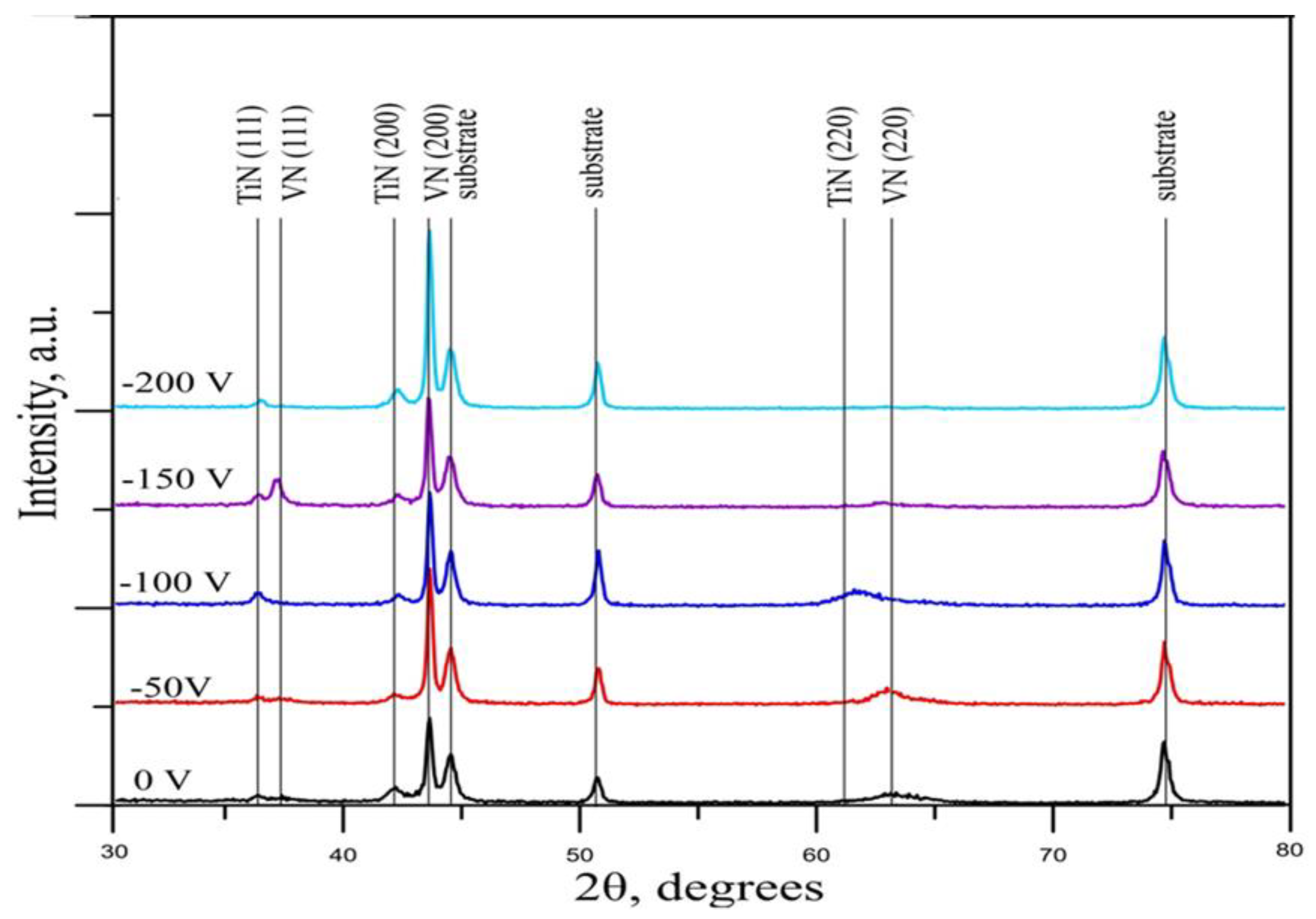
Figure 2.
FTIR reflectance spectra of VN films deposited at different bias voltages and the substrate.
Figure 2.
FTIR reflectance spectra of VN films deposited at different bias voltages and the substrate.
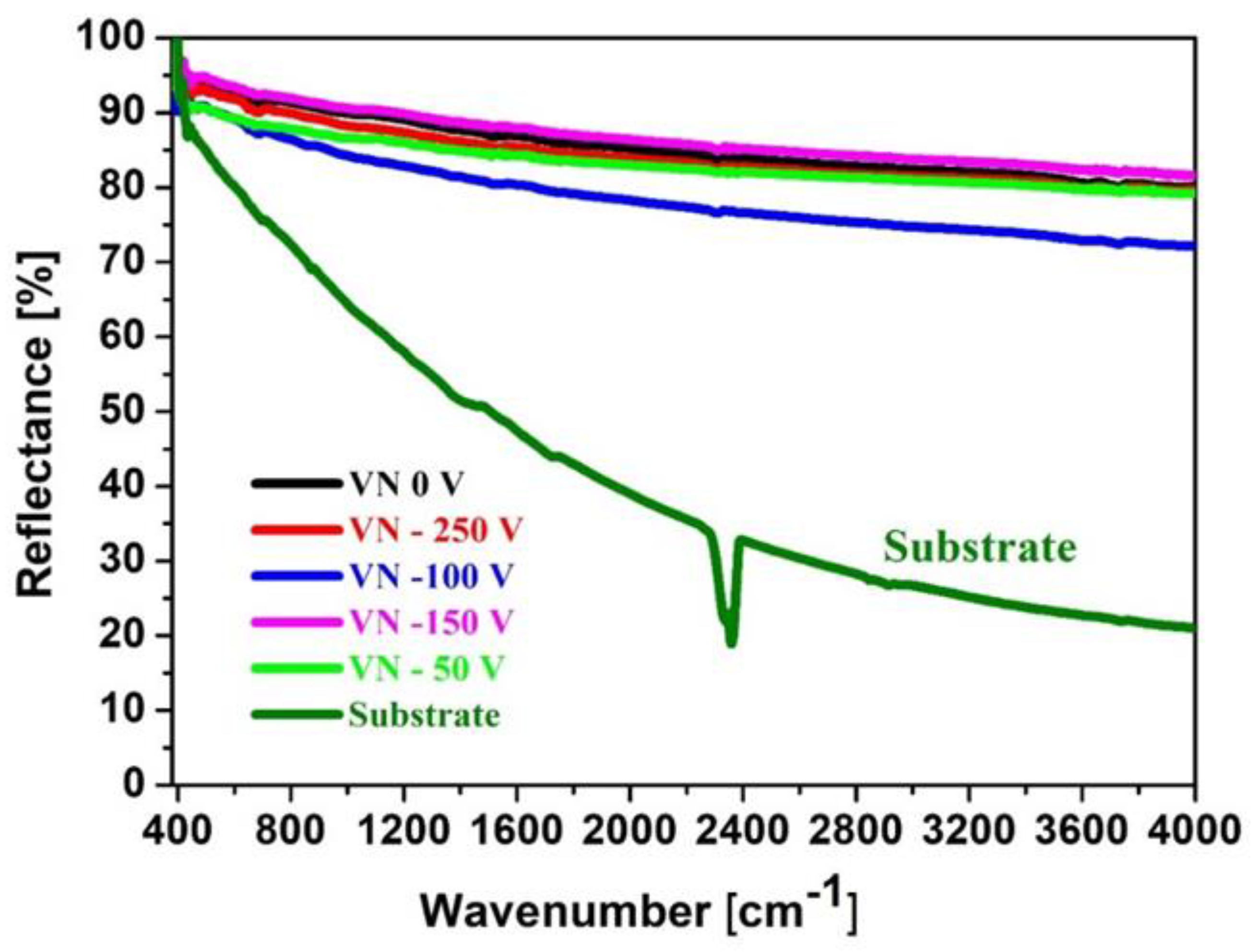
Figure 3.
More detailed FTIR reflectance spectra of VN films at different bias voltages.
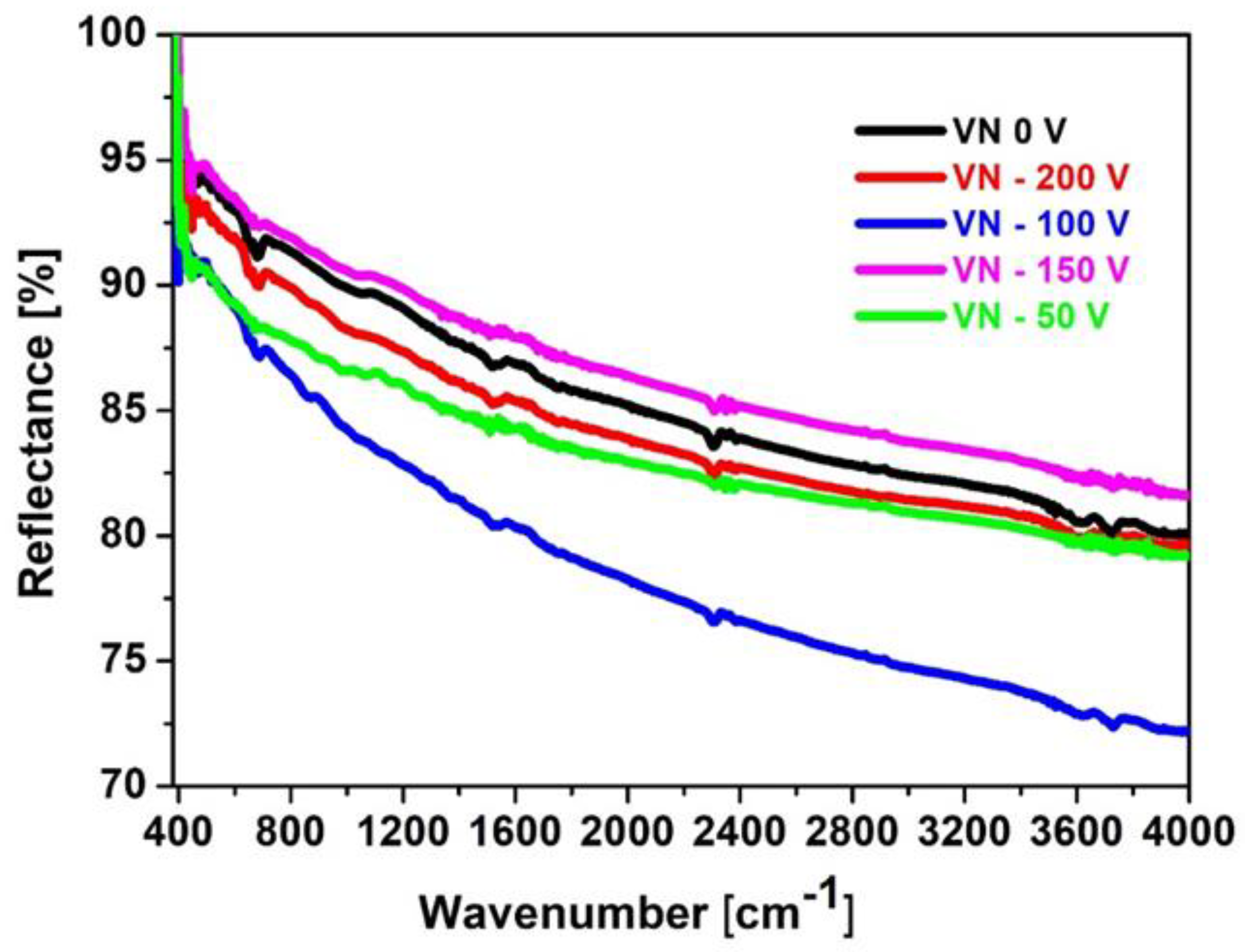
Figure 4.
SEM cross-section images of VN coatings, produced at a bias voltage of: (a) 0 V; (b) – 50 V; (c) – 100 V; (d) – 150 V; (e) – 200 V; (f) chemical composition of VN coatings on 304 L stainless steel substrates by EDX analysis.
Figure 4.
SEM cross-section images of VN coatings, produced at a bias voltage of: (a) 0 V; (b) – 50 V; (c) – 100 V; (d) – 150 V; (e) – 200 V; (f) chemical composition of VN coatings on 304 L stainless steel substrates by EDX analysis.
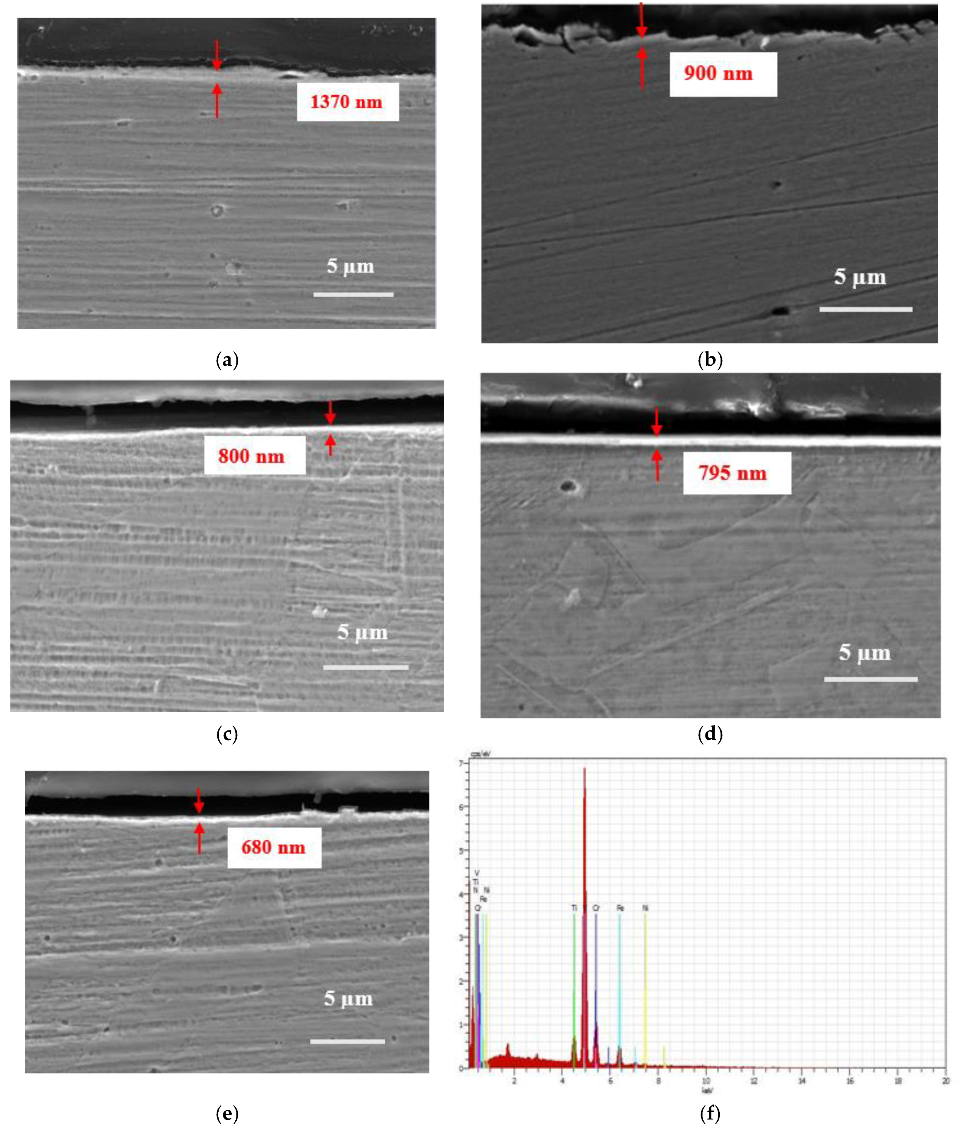
Figure 5.
Three-dimensional AFM images of VN films, deposited at a bias voltage of: (a) 0 V; (b) – 50 V; (c) – 100 V; (d) – 150 V; (e) – 200 V.
Figure 5.
Three-dimensional AFM images of VN films, deposited at a bias voltage of: (a) 0 V; (b) – 50 V; (c) – 100 V; (d) – 150 V; (e) – 200 V.
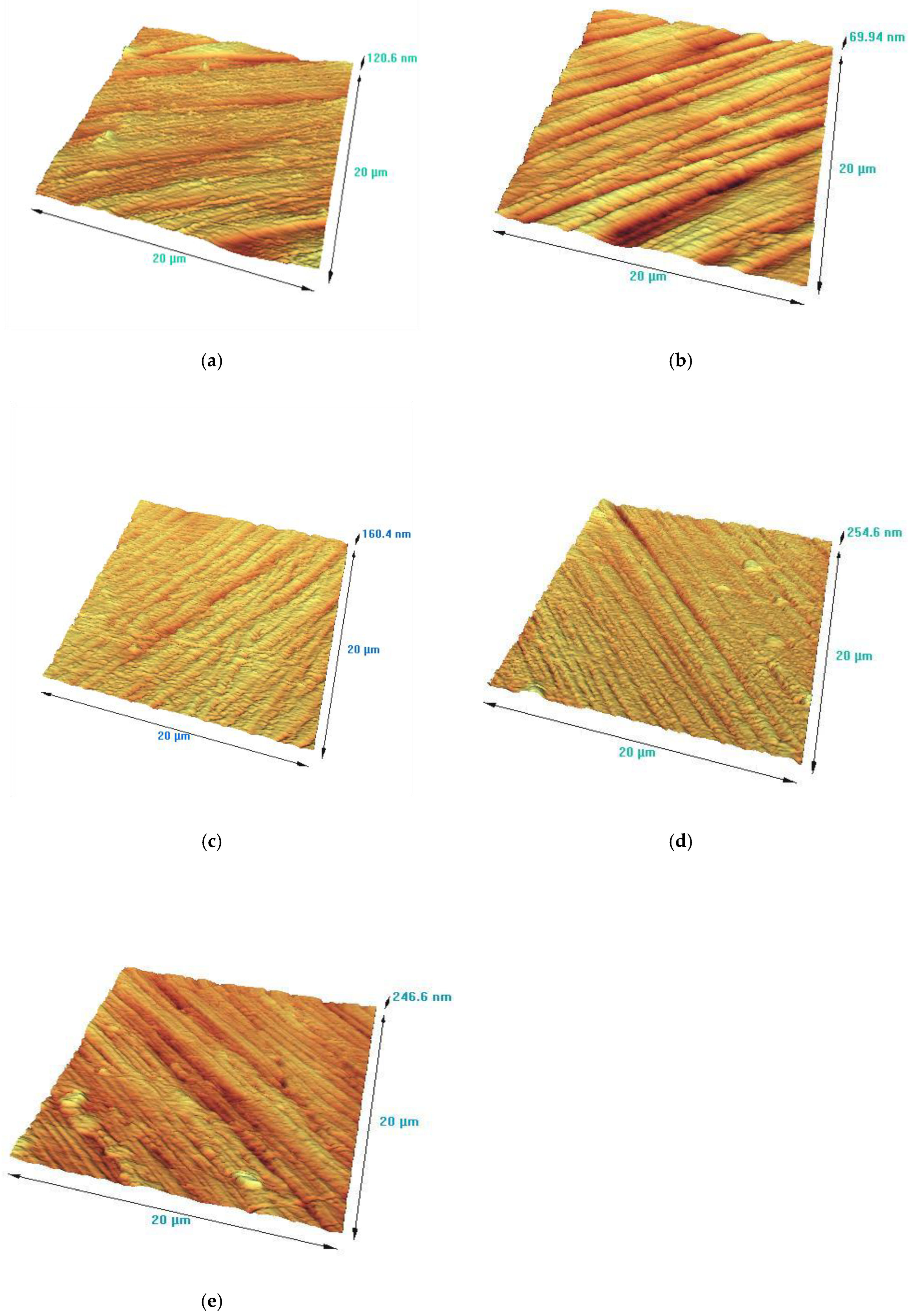
Figure 6.
Hardness and elastic modulus of VN coatings as a function of a negative bias voltage.
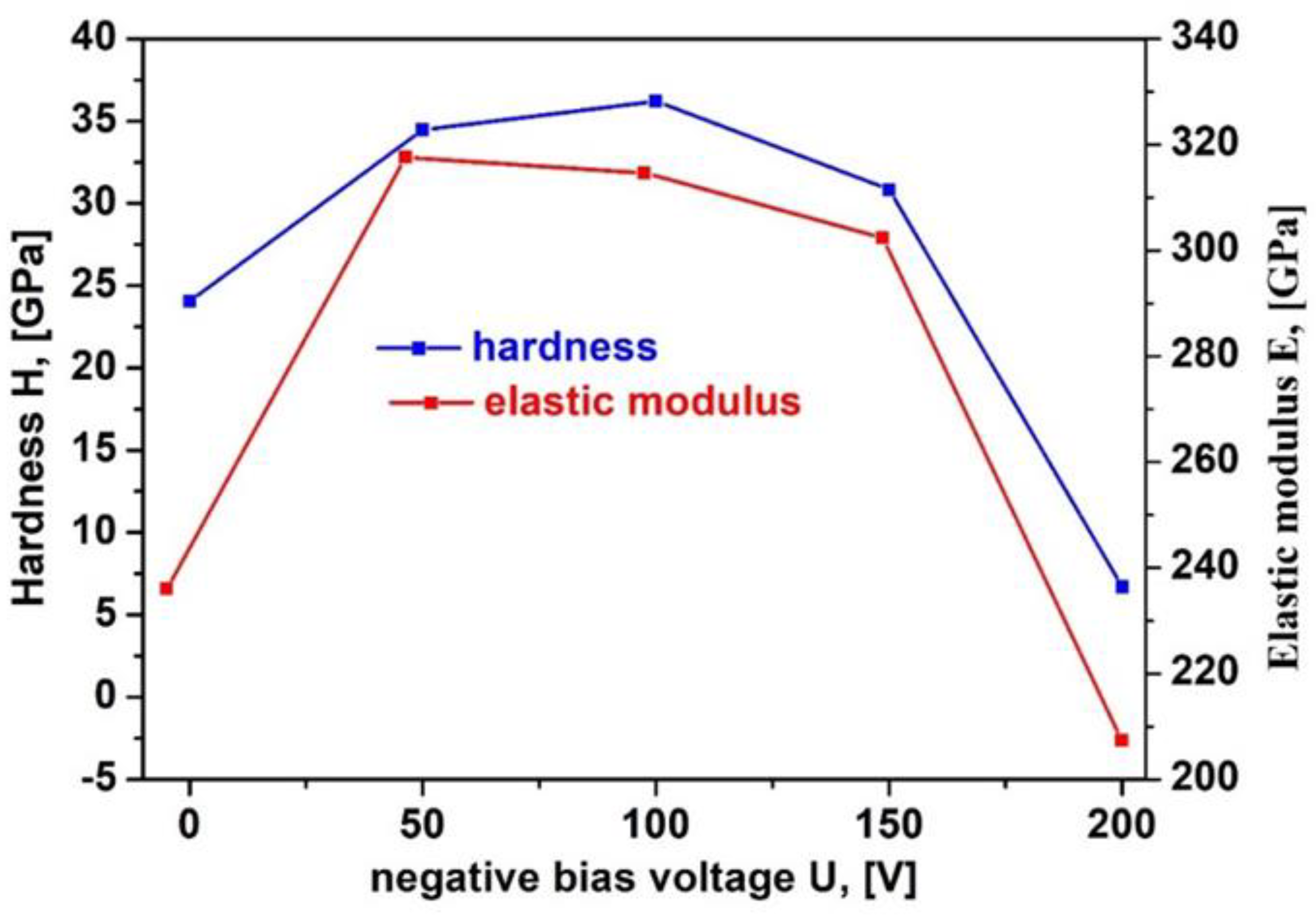
Figure 7.
Load - indentation depth curve for VN films with a constant applied force of 10 mN at a bias voltage of: (a) 0 V; (b) – 50 V; (c) – 100 V; (d) – 150 V; (e) – 200 V.
Figure 7.
Load - indentation depth curve for VN films with a constant applied force of 10 mN at a bias voltage of: (a) 0 V; (b) – 50 V; (c) – 100 V; (d) – 150 V; (e) – 200 V.
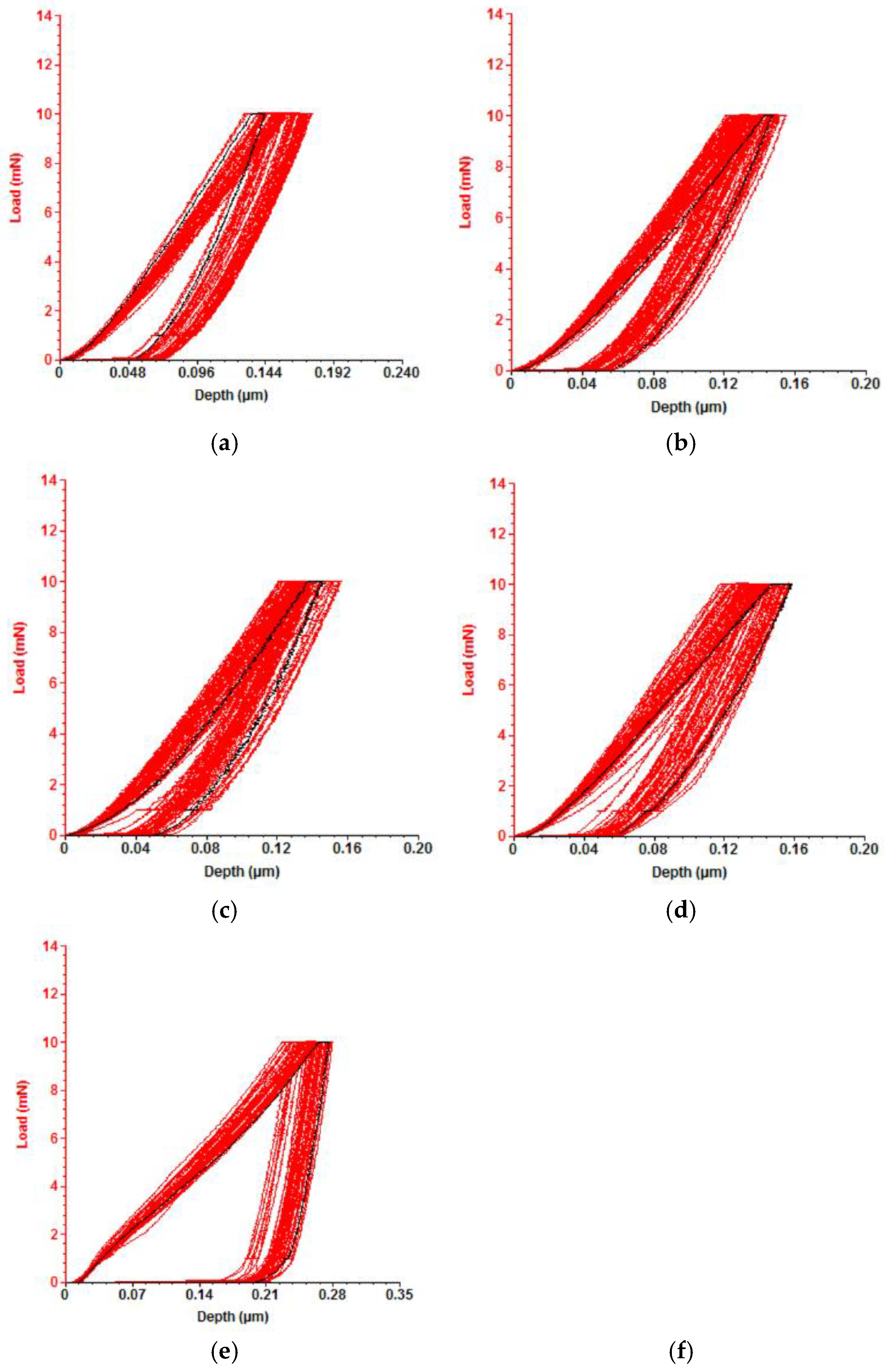
Figure 8.
Variation of the VN films friction coefficients with the substrate bias voltages at different loads.
Figure 8.
Variation of the VN films friction coefficients with the substrate bias voltages at different loads.
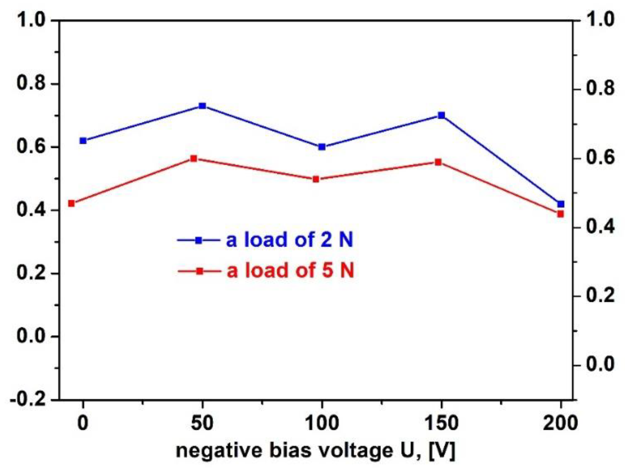
Figure 9.
Corrosion potential of magnetron - sputtered VN coatings in 0.1 M NaCl- containing phosphate buffer solution (pH = 7.0) as a function of time for reaching equilibrium; electrolyte: phosphate buffered saline, pH = 7.0 containing 0.1 M NaCl.
Figure 9.
Corrosion potential of magnetron - sputtered VN coatings in 0.1 M NaCl- containing phosphate buffer solution (pH = 7.0) as a function of time for reaching equilibrium; electrolyte: phosphate buffered saline, pH = 7.0 containing 0.1 M NaCl.
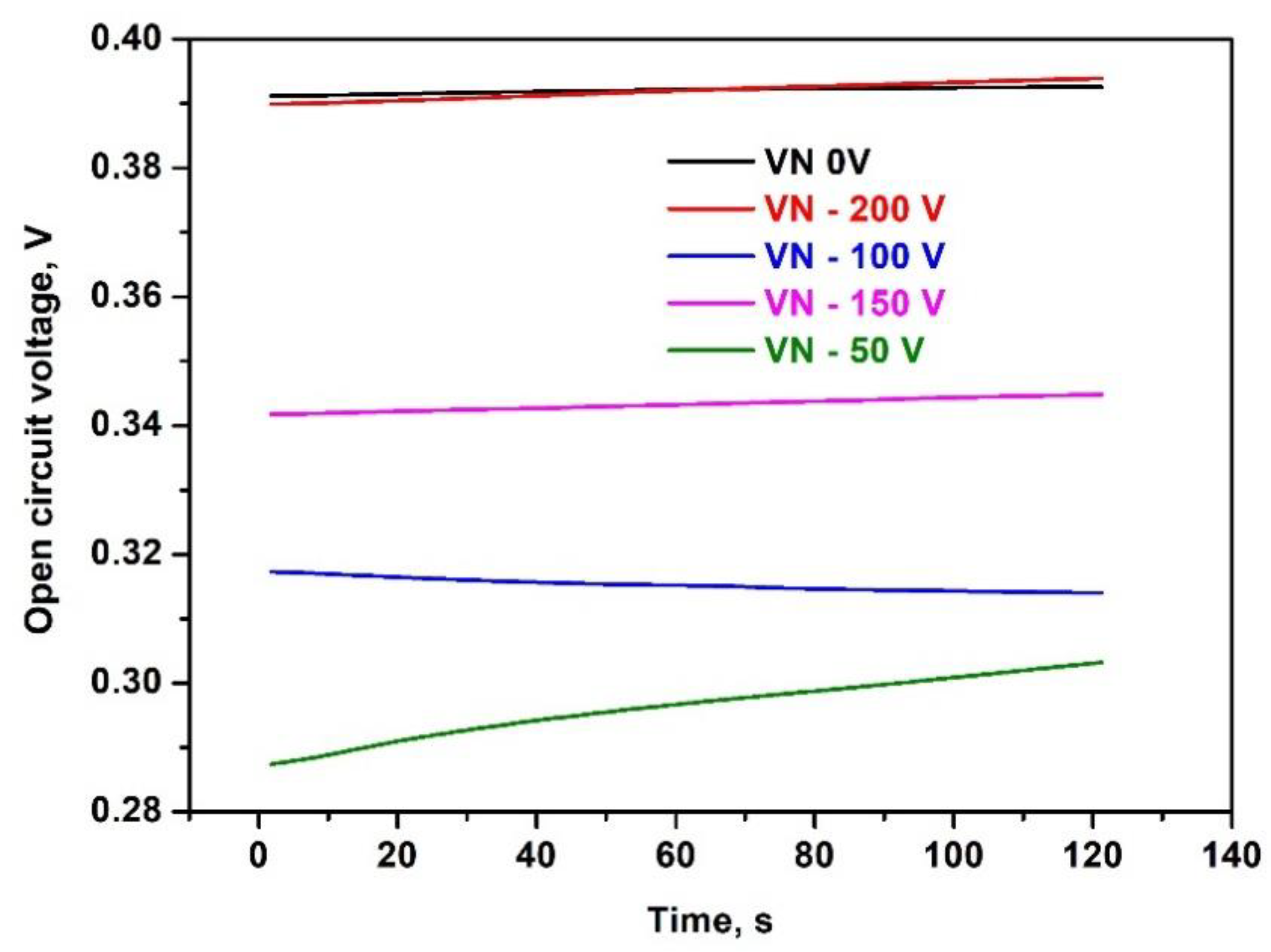
Figure 10.
Impedance spectra of VN-coated samples in 0.1 M KCl, containing 5 mM K4[Fe(CN)6] and 5 mM K3[Fe(CN)6]; (a) 0V; (b) – 200 V; (c) – 100 V; (d) – 150 V; (e) – 50 V; (f) Impedance spectra of VN films, deposited at different bias voltages.
Figure 10.
Impedance spectra of VN-coated samples in 0.1 M KCl, containing 5 mM K4[Fe(CN)6] and 5 mM K3[Fe(CN)6]; (a) 0V; (b) – 200 V; (c) – 100 V; (d) – 150 V; (e) – 50 V; (f) Impedance spectra of VN films, deposited at different bias voltages.
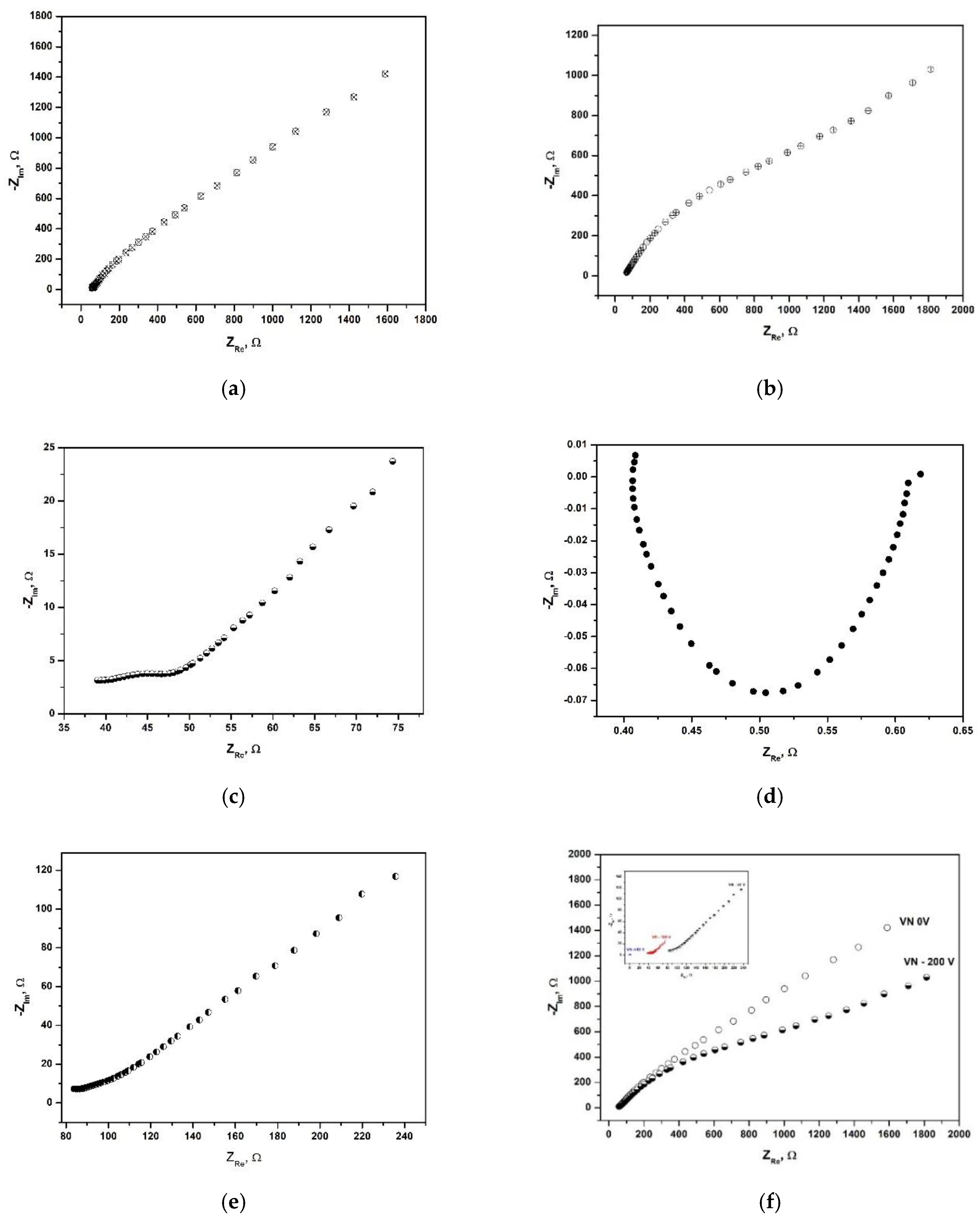
Figure 11.
Polarization curves (cyclic voltammograms) of VN- coated samples, scan rate 0.05 V/s; electrolyte 0.05 M phosphate buffer, pH = 7.0 containing 0.1 M NaCl, room temperature.
Figure 11.
Polarization curves (cyclic voltammograms) of VN- coated samples, scan rate 0.05 V/s; electrolyte 0.05 M phosphate buffer, pH = 7.0 containing 0.1 M NaCl, room temperature.
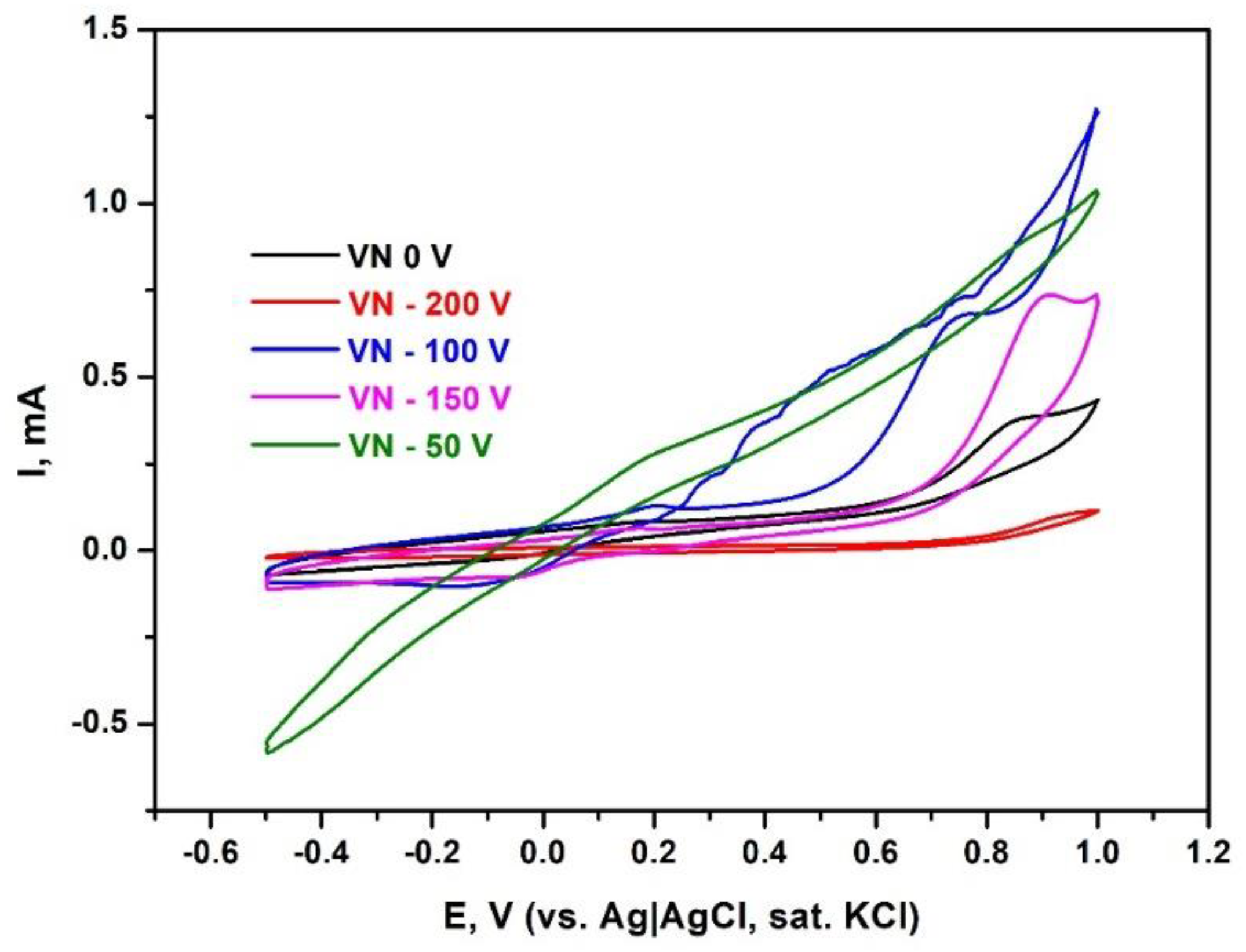

Table 1.
Mechanical characteristics of the deposited VN films at various bias voltages.
| VN samples | Hardness, GPa | Elastic modulus, GPa | H/E ratio | H3/E2 ratio |
|---|---|---|---|---|
| 0 V | 24.00 ± 4.03 | 236.02 ± 27.86 | 0.101 | 0.248 |
| - 50 V | 34.50 ± 5.03 | 316.45 ± 35.66 | 0.107 | 0.001 |
| - 100 V | 36.20 ± 5.60 | 317.73 ± 32.86 | 0.114 | 0.478 |
| - 150 V | 30.83 ± 4.89 | 302.38 ± 44.75 | 0.102 | 0.321 |
| - 200 V | 6.7 ± 0.64 | 207.36 ± 23.09 | 0.032 | 0.007 |
Disclaimer/Publisher’s Note: The statements, opinions and data contained in all publications are solely those of the individual author(s) and contributor(s) and not of MDPI and/or the editor(s). MDPI and/or the editor(s) disclaim responsibility for any injury to people or property resulting from any ideas, methods, instructions or products referred to in the content. |
© 2026 by the authors. Licensee MDPI, Basel, Switzerland. This article is an open access article distributed under the terms and conditions of the Creative Commons Attribution (CC BY) license (http://creativecommons.org/licenses/by/4.0/).
Copyright: This open access article is published under a Creative Commons CC BY 4.0 license, which permit the free download, distribution, and reuse, provided that the author and preprint are cited in any reuse.


