
Submitted:
21 February 2026
Posted:
26 February 2026
You are already at the latest version
Abstract
In this study, the growth of high-quality graphite single crystals from a molten metal flux at atmospheric pressure was optimized. The crystals were precipitated from a saturated iron-carbon solution by slowly cooling (4 °C/h) from a maximum temperature to reduce the carbon solubility. The graphite flakes were >25 square millimeters in area and >10 of microns thick, with individual crystal grains as large as 1.2 mm2. The crystals were (0002) oriented, as determined by x-ray diffraction. The high structural quality of the graphite crystals was verified by Raman spectroscopy. For graphite with the natural distribution of carbon isotopes, the G-peak at 1580 cm-1 was narrow (~12 cm-1) and the defect peak (D-peak) was absent. To demonstrate the process versatility, graphite crystals enriched in the 13C isotope were grown. The Raman peak shifted to 1520 cm-1 for graphite crystals en-riched to 99% 13C. The etch densities from defect sensitive etching ranged from 0 to 1.6x10⁸ etch pits per cm2. The process was refined by examining the crystal size and quality as functions of the carbon concentration in the starting sources, the carrier gas composition, and maximum temperature. The simplicity of this process suggests it can be scaled to produce very large graphite crystals that would be suitable for a wide range of technologies.
Keywords:
graphite
; crystal
; optimization
; characterization
; growth
; solvent
; atmospheric-pressure
; high-temperature
1. Introduction
Graphite is an allotrope of carbon with extraordinary properties, garnering extensive interest for its potential applications in novel devices and electronics. It consists of carbon layers arranged in a hexagonal lattice held together by sp2 covalent bonds, forming sheets. These layers are held together by weak van der Waals forces; forming graphite crystals[1]. Due to the directional bonding that is stronger along the a-axis than along the c-axis , graphite’s properties are highly anisotropic. For example, its in-plane thermal conductivity is 200 times higher than the cross-plane thermal conductivity [2,3]. The lack of dangling bonds on the surface of graphite crystals permits a high degree of chemical inertness [4], making graphite a stable, nontoxic, safe alternative to other thermal and electric conductors.
The sources for the highest quality graphene are either natural, geological graphite, or Kish graphite crystals [5]. However, size, quality, and impurity concentrations are not controlled in the graphite crystals from these sources. Monolayer or a few layers of graphene are synthesized by CVD on metal substrates [6] and the thermal conversion of silicon carbide single crystals [7], but their quality is lower than that produced by the exfoliation of bulk graphite. While there is a plethora of literature on iron-carbon solutions, due to its importance to the manufacture of steel, there have been surprisingly few studies on graphite crystal growth from molten metal solutions. The focus of most prior studies was on steel production with little attention to the kish graphite. The most detailed study was done by Austerman [8] nearly sixty years ago. He found supersaturation of an iron flux with carbon produced a variety of macrostructures of graphite.
Graphite’s weak interplane attraction also allows layers to be easily separated into monolayer graphene via mechanical exfoliation [9]. Aside from being an ultra-thin material (0.334 nm thick), graphene’s properties are enhanced beyond that of normal graphite, including low density, high surface area-to-volume ratio, ultra-high electron mobility (200,000 cm2/Vs), thermal conductivity (5000 Wm/K), high optical transparency (97.4%), and enhanced mechanical properties [9,10,11]. These properties make graphene suitable for growing industries such as electric vehicles, lightweight electronics, transistors, and energy storage such as in rechargeable batteries [12,13,14]. The high Young’s modulus (1 TPa) lends itself to applications in high-performance flexible electronics such as flexible photovoltaic cells or LED displays [15]. Graphene also finds applications in data storage, logic gates, and magnetic field sensors through the use of spintronics [16]. Graphene is attractive for spintronics due to its long electron spin diffusion lengths, long spin lifetimes, and difference in nuclear spins between the 12C (nuclear spin 0) and 13C (nuclear spin 1/2) isotopes [17,18,19]. Recently, we have demonstrated that 13C doping in 12C graphite leads to splitting of the Landau level transitions under an out-of-plane magnetic field [20]. In addition, isotopically pure graphite exhibits enhanced thermal conductivity due to the reduction of phonon scattering by the isotope mass differences of natural carbon (99 at% 12C, 1 at% 13C) [21].
The present study optimizes graphite crystal growth around quality, grain area, and isotopic enrichment from a molten metal solution, specifically, iron. The process conditions examined include the mass fraction of carbon, cover gas composition, and maximum temperature. The quality of the graphite crystals was assessed by the Raman spectroscopy, 002 XRD diffraction, and defect sensitive etching (DSE). Crystal grain sizes were measured by optical microscopy. These parameters point towards the ideal conditions to produce large area graphite crystals while minimizing unintentional/undesired defects.
2. Materials and Methods
2.1. Metal Flux Growth
Transition metals (including Fe, Ni, and Co) are all suitable solvents for carbon. Iron was selected for these experiments because of its relatively low cost. In these experiments, mixtures of carbon (99.995%) and iron (99.99%) were heated in an alumina (99.9%) crucible under an inert gas. The temperature control schedule was varied between each optimization experiment set. Essentially, the iron is melted and the carbon dissolves into the melt, forming an iron-carbon solution. It is then slowly cooled causing the carbon to supersaturate and precipitates from the solution, forming bulk graphite crystals on the metal surface. Graphite crystals were then mechanically exfoliated from the ingot using thermal release tape. Figure 1,below, is the temperature control schedule for maximum temperature optimization with an inset depicting the resulting graphite crystals on an iron boule.
Five graphite samples of various isotopic concentrations were synthesized by varying the ratio of natural carbon and graphite powder that was enriched to 99% with the 13C isotope. These samples contained 1%, 20%, 60%, and two samples contained 99% 13C.
2.2. Grain Size Measurements
Optical microscope images of typical graphite flakes are shown in Figure 2. Figure 2a presents an isotopically enriched 13C graphite flake and arrows distinguish visible defects along the surface in Figure 2b. A parallel of such for natural graphite crystals is shown in Figure 2c and Figure 2d. Graphite flakes were exfoliated from the boule surface, then imaged with objectives varying from 25 to 1000x magnification. The topology of the crystal flake consisted of large flat facets separated by wrinkles, cracks, and grain boundaries. Individual grain size areas were measured by using the polygon feature of ImageJ software [22]. To collect statistics on the graphite grain properties, ten images were taken of 10 selected flakes from each experiment with flat, unobscured, and distinguishable grains. An example of such is provided below in Figure 2c.
2.3. Raman Analysis
The crystal quality and isotope concentrations in the graphite flakes were verified by Raman spectroscopy. Spectra were taken at room temperature with a Bruker 2 Senterra employing a 532 nm laser with a power of 20 mW collected in backscattering configuration. Two spectral regions were analyzed. The first region is the “G-peak” which is between 1520cm-1 (for 13C-enriched graphite) and 1580cm-1 (for graphite with natural distribution of isotopes). The full width at half maxima (FWHM) of the G-peak is indicative of the crystal quality and the exact peak position shifts with isotopic concentration. The second region is the “D-peak”, or defect peak, whose intensity is indicative of the defect concentration in the graphite [23]. The G-peaks were fit with Lorentzian curves to obtain a FWHM.
Three isotopically enriched graphite samples were mapped using a 31x31 point Raman scan across a 15x15 µm region to test for consistency across the surface of the sample. The FWHM of each point was determined with a Python program, creating a statistical distribution of peak widths that can be compared across different samples. Raman mapping was performed at room temperature using a Horiba LabRAM HR800 Confocal Raman Microscope system that is equipped with a thermoelectrically cooled CCD detector. A 532 nm laser and a 100× objective lens was used. Laser power was kept at 6.8 mW during Raman mapping. A 600 grooves/mm grating was used which corresponds to an instrument resolution of ~2 cm-1.
2.4. X-Ray Diffraction Analysis
In addition to Raman spectroscopy, Cu Kα X-ray diffraction (XRD) patterns from 10-80° were collected for all optimization experiments using and Rigaku Miniflex Tabletop XRD at 30 mA. Similar to Raman spectroscopy, the quality of the graphite crystals was quantified with the XRD FWHM of the 0002 peak. Narrow diffraction peaks are further evidence of crystal integrity.
2.5. Defect Sensitive Etching
The dislocation density of graphite crystals was assessed using DSE. The molten eutectic mixture of KOH and NaOH reacts with graphite at surface defect sites, producing etch pits. The graphite crystals were etched at 490 °C for 280 seconds. The crystals were then quenched to room temperature in water to remove the hydroxide. Patel and Bahl [24] demonstrated that the resulting etch pits correlate with edge and screw dislocations. The morphologies of these pits are pointed termination and some can have flat termination as illustrated in Figure 3 below.
Edge dislocations occur when there is an additional crystal plane that terminates mid-lattice perpendicular to the Burgers vector inducing tensile strain [25]. A screw dislocation occurs when an atom in a lattice is slightly displaced causing interlayer shift parallel to the Burgers vector [26].
The area of the pits was determined from using the ImageJ software [22]. The etch pits in five representative regions were imaged from each etched graphite flake. The average area of pits was weighed with the number of pits used to represent each sample’s overall etch pit size.
The etch pit density was calculated by dividing the number of etch pits over the crystal area encompassed in each image. To illustrate the etch pits in detail, scanning electron microscope (SEM) images were taken using a Zeiss GeminiSEM 500 with an acceleration voltage of 0.5 kV and aperture of 20 µm using the InLens detector.
2.6. Crystal Growth Optimization
The goal of these experiments was to optimize the process to produce large area crystals of high quality. The relevant parameters investigated included the carbon mass percent, cover gas composition, and maximum temperature. The graphite crystal quality was assessed with the FWHM of the XRD (0002), Raman D-peak FWHM, and DSE etch pit densities. All experiments were performed using a R.D. Webb Red Devil Graphite insulated box furnace.
The temperature profile for the carbon composition experiments consisted of a heating to 1500 °C at 75 °C/hour in an argon atmosphere and holding for 24 hours. Then the molten metal solutions were cooled at 4 °C/hour to 1350 °C and finally quenched at 75 °C/hour to room temperature. The carbon solubility in molten iron is 6.67 mass percent[27]. Eight experiments were conducted to ascertain the carbon mass percent that maximizes grain size and quality of the precipitated graphite. The graphitic carbon mixed with iron shots was varied from 2.1 to 6.7 mass percent. These compositions represent the lowest possible composition and saturation in iron, respectively, for graphite precipitation. The composition that produced the largest grain size average was then used for both the cover gas experiments and the maximum temperature experiments.
Two different gases were used to determine whether the cover gas composition affects crystal growth: Ultra-High Purity (UHP) Nitrogen (99.99%) and UHP Argon (99.99%). The temperature schedule was different from the composition experiments for consistency between the two. The schedule began with heating to 1450 °C at 1200 °C/hour, then to 1500 °C at 600 °C /hour. The flux was held at that temperature for 24 hours. Once this dwell was over, the furnace was cooled to 1000 °C and dwelled for 24 hours before being quenched to room temperature via natural cooling.
To find the optimal temperature, the temperature schedule was a heating ramp to a varied dwell temperature (X). Initially the chamber was heated to X-50 °C at 1200 °C/hour, then to X °C at 600 °C/hr. The furnace was held at X °C for 24 hours followed by cooling at 4 °C/hour to X-50 °C. After which, the furnace was quenched to room temperature at 1200 °C/hour. X was evaluated from 1125 °C to 1550 °C in increments of 25 °C (i.e. X ).
3. Results and Discussion
3.1. Grain Size Optimization
A collection of box plots representative of each parameter in the optimization experiment set is presented in Figure 4. The grain-size is measured against the independent variables in the left column, while the associated temperature schedules are shown on the right abbreviated from 1000 °C along the y-axis.
Figure 4a illustrates graphite crystal size as a function of the initial amount of carbon loaded. Since 2.1 wt.% did not produce crystals that could be exfoliated, it was omitted from the figure. Due to the high standard deviation, no correlations can be confidently drawn. On the right, the y-axis begins at 1000 °C to highlight the cooling step following the dwell. The maximum crystal grain size occurred at 5.8 wt.% carbon composition; therefore, it was selected as the composition for the remaining experiments.
There was no statistical correlation between the cover gas and crystal grain size (Figure 4b). This is unsurprising given neither gas is expected to react with carbon nor iron in the molten metal solution. Consequently, nitrogen was arbitrarily selected as the cover gas for the final set of optimization experiments.
In 4c, the maximum temperature was varied from 1550 °C to 1150 °C below which the solution was no longer molten. Smaller crystals did form at lower temperatures; however, they were significantly smaller than those of the higher temperatures. Crystals grown at 1250 °C were significantly smaller than the others (900 µm2), likely an outlier. The crystal area increases with temperatures up to 1400 °C . This implies the existence of an optimum temperature for crystal size. The temperature versus time profile is different for each experiment set, disqualifying comparison between the different test variables.
3.2. Raman Analysis
3.2.1. Optimization Characterization
Single Raman spectra were taken from three different flakes and averaged together to represent each experiment. All experiments had a lack of a D-peak despite some of the conditions used to grow the crystals. The FWHM and position of the G-peak remained consistent around 14 cm-1 at 1580 cm-1 for all experiments. The only exception to this observation is the compositional optimization which showed a linear decrease in FWHM from 15.6 at 4.2 carbon wt. % to 14.2 at 6.7 wt.% C. The abundance of carbon may prevent certain intrinsic defects like Stone-Wales or other sources of strain.
3.2.2. Isotopic Enrichment
Raman analysis indicates high quality isotopically controlled graphite crystal in Figure 5 for all samples. Regardless of growth conditions none of the graphite crystals had the ‘D-peak,’ at 1350cm-1. Narrow graphite ‘G-peaks’ indicate a low crystal strain and a high degree of crystallinity [3,4]. The FWHM of the Raman G-Peak broadens when the graphite contained isotopes mixtures. An isotopically pure sample has a FWHM of 12.2 cm-1 for both carbon isotopes, whereas a mixture of 40% 12C/60% 13C has a peak width of 20.8 cm-1, due to isotopic disorder. Isotopically pure graphite has superior phonon transport properties and functions as a better thermal and electrical conductor [2,3,4]. The G-peak shift is sensitive to isotopic concentration in the graphite due to the mass differences between carbon isotopes changing the vibrational frequency of the crystal bonds. Crystals with 1% 12C content have a G-peak shift of 1520cm-1, and crystals with a 99% 12C content have a G-peak shift of 1580cm-1. Figure 5c shows that the G-peak shift is linear with respect to isotopic concentration, allowing isotopic concentration to be readily determined by Raman spectroscopy.
Raman mapping was used to test for consistency across the crystal surface. 960 measurements were taken in a 15 x 15 μm grid across the samples of varying isotopic concentration, and histograms of the G-peak FWHM are shown in Figure 6. Overall, the variance of the FWHM is small indicating a high degree of sample uniformity. The isotopically mixed samples showed a larger standard deviation in the peak width than isotopically pure samples. This indicates that the isotopically pure samples are more uniform across the sample surface than the isotopically mixed samples. Pairing the increased non-uniformity with the wider median FWHM, isotopically mixed graphite shows a higher propensity for defect inclusions in the crystal structure.
3.2. X-Ray Diffraction
XRD patterns were taken from exfoliated graphite crystals except for the 2.1 weight percent carbon source from which no crystals could be exfoliated. Crystal quality was comparable across all conditions, regardless of the source carbon weight percent. Figure 7 illustrates the existence of a non-optimal range producing very disordered crystals from 4.6 to 5.8 wt. % C in Fe. The narrow 002 plane diffraction pattern at 26° seen in Figure 5b was typical of crystals grown outside the 4.6-5.8 wt. % C in Fe range. These oddly contradict the Raman FWHM analysis suggesting that there may be defects along the c-direction which would appear below the sensitivity range of the Raman microscope used in this work (>100 cm-1).
Unexpectedly there is no relation between 002 FWHM and temperature or cover gas composition. It was expected that as the crystals get larger, more defects will be present due to the larger sample volume. As the defect quantity increases, so too does the strain in the crystal bulk reflected by the increasing FWHM. The cover gas composition did not have a significant impact on the diffraction patterns. The nitrogen and argon samples both had 002 FWHM’s of 0.12°. A similar trend was noted in the temperature optimization series with all but one sample oscillating around 0.12 ± 0.02°.
3.3. Defect Sensititive Etching
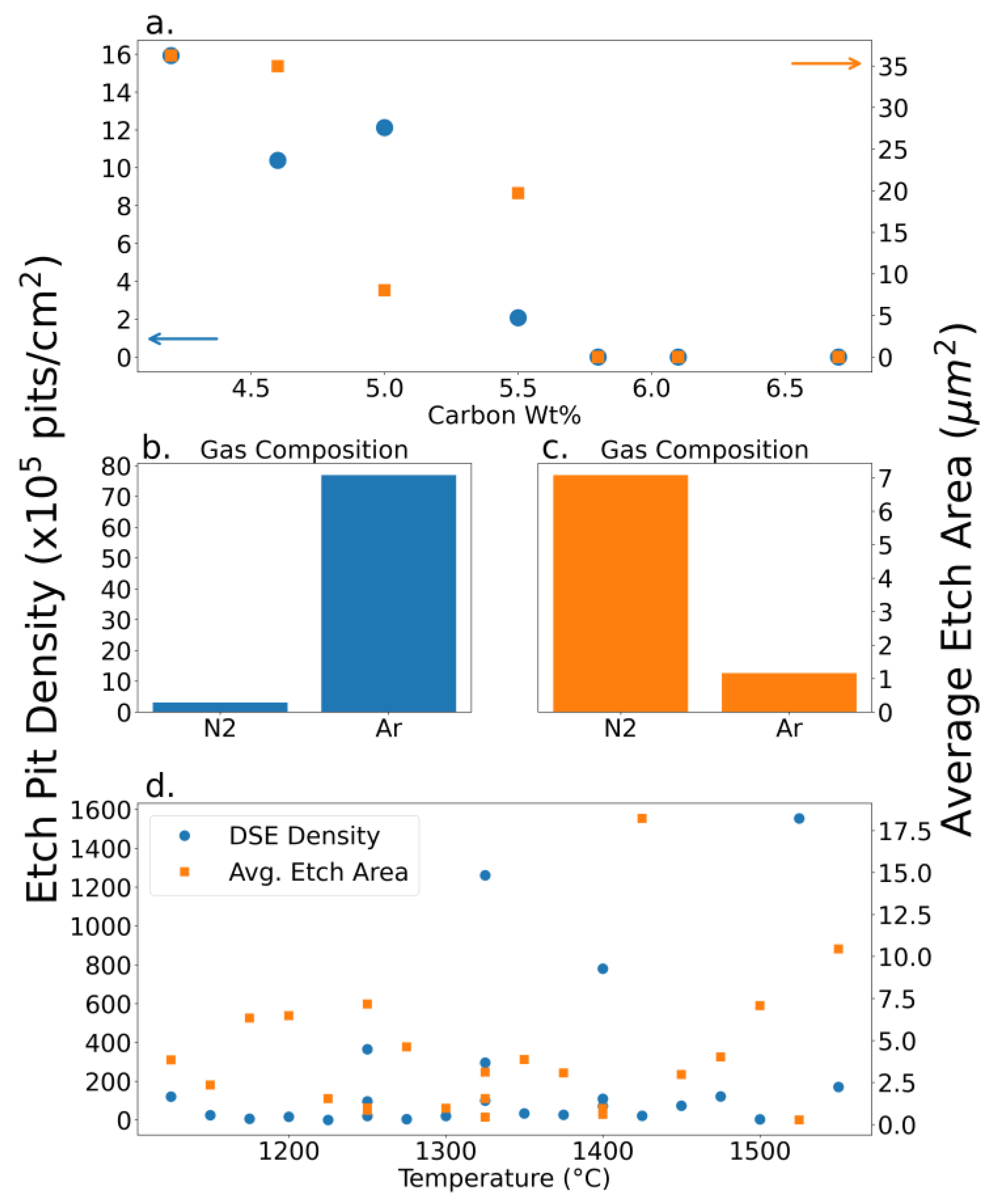
DSE revealed etch pit densities ranging from 0 to 1.6x10⁸ pits/cm2. The lack of etch pits observed in the some of the compositional optimization experiments indicates pristine crystal with minimal high energy sites susceptible to etching. The density of these pits can be correlated to the abundance of edge and screw dislocations due to defects. Hence, the etch pit density can be correlated with defect density along the surface since the etching is surface sensitive. An example of such dislocations is provided in Figure 8 below.
As shown in Figure 8a, there are several facets to the defects present as previously shown in Figure 3. These DSE etch pits varied in diameter hence it is insightful to look into how the optimization parameters can affect their size. Additional samples were etched to reveal potential trends with respect to growth conditions throughout the growth optimization experiments summarized in Figure 7. There did not appear to be any consistent trend regarding the location of these pits. They seemed to have no preference for macroscopic defects like grain boundaries or wrinkles. Occasionally these pits would have a crystallographic arrangement relative to each other, but more often they had no apparent preference. Etch pits observed across the optimization experiments are shown in Figure 9.
The first trend in Figure 9a is the lack of defects after 5.8 wt. %. An explanation may be that the oversaturation of the solvent minimizes surface defects. Another possible explanation is that the etchant’s surface sensitivity outweighs that of XRD. This means that, despite having a narrower 002 diffraction peak, there may be more defects than accounted for along the surface specifically.
DSE shows that graphite crystals grown in nitrogen induces larger (Figure 9c) but fewer instances (Figure 9b) of defects. Why that is, remains unclear. A theory is that the solubilization of nitrogen in iron possibly interferes with the way that graphite is precipitated inducing specific defect sizes.
In Figure 9d, crystals grown at different maximum temperatures show little correlation with defect topology. From the data provided, there can be no correlation confidently claimed between defects in graphite crystals and the temperature at which they are grown. Since smaller crystals are grown at lower temperatures, it is not unreasonable to expect fewer defects due to the lack of bulk defects produced.
4. Conclusions
The largest graphite single crystal grain was grown with 5.8 wt.% carbon source at 1400 °C under a nitrogen atmosphere. It was 18% larger (3.4 x 105 µm2) than the second largest crystal grown at other conditions (2.8 x 105 µm2). The optimized APHT solvent growth method produces high quality bulk graphite with a Raman G-peak FWHM of less than 10 cm-1 and XRD (0002) diffraction peaks FWHM as low as 0.03°. These graphite crystals are also large with grain sizes on the order 1.2 square millimeters. Furthermore, these grains are relatively thick compared to film methods resulting in 20+ µm thick free-standing crystals. This synthesis method also allows for good control of isotopic enrichment as demonstrated in the shift of the G-peak.
In conclusion, the optimal conditions for graphite growth coincide with those reported by Austerman et al [31], however, contrary to their findings, nitrogen was more favorable for graphite growth under the same conditions: their average grain size was 25% larger (2.5 x105 µm2 versus 2.0 x105 µm2). Conditions to grow the largest are a graphite crystal grains are 5.8 wt.% carbon mixture heated to 1450 °C under a nitrogen atmosphere though there would be few large dislocations relative to other conditions. However, to minimize dislocations, the same composition could be heated to 1500 °C and produce less consistent, but larger crystal grains. Therefore, the metal flux method can be tailored to produce crystals with moderate control over their dislocations and grain sizes without jeopardizing quality. Future investigations over controlled nucleation will lead to the scalable growth of large graphite single crystal via the metal flux method.
Author Contributions
For research articles with several authors, a short paragraph specifying their individual contributions must be provided. Conceptualization, J.E., T.P. and D.E.; methodology, T.P.; software, T.P. and D.E.; validation, J.E.; formal analysis, T.P., D.E., M.S. and R.H.; investigation, T.P., D.E., I.T. , and R.H.; resources, J.E.; data curation, T.P., D.E., and R.H.; writing—original draft preparation, T.P., D.E., and J.E; writing—review and editing, T.P., D.E., and J.E.; visualization, T.P. and D.E.; supervision, J.E. and P.A.; project administration, J.E.; funding acquisition, J.E. All authors have read and agreed to the published version of the manuscript.
Funding
Support for crystal growth was provided by the Office of Naval Research Award numbers N00014-20-1-2474 and N00014-22-1-2582, and the Air Force Office of Scientific Research award number FA9550-22-1-0125. G.Y. was supported by NSF Grant No. DMR-1760668. R. H. acknowledges support by DOE Office of Science Grant No. DE- SC0020334 Subaward S6535A.
Data Availability Statement
Dataset available on request from the authors.
Conflicts of Interest
The authors declare no conflicts of interest. The funders had no role in the design of the study; in the collection, analyses, or interpretation of data; in the writing of the manuscript; or in the decision to publish the results.
Abbreviations
The following abbreviations are used in this manuscript:
| XRD | X-ray diffraction |
| FWHM | Full-width at half-maximum |
| SEM | Scanning Electron Microscope |
| CVD | Chemical vapor deposition |
| DSE | Defect Sensitive Etching |
References
- Owuor, P. S.; et al. Roadblocks faced by graphene in replacing graphite in large-scale applications. Oxf. Open Mater. Sci. 2020, vol. 1(no. 1), itab004. [Google Scholar] [CrossRef]
- Primak, W.; Fuchs, L. H. Electrical Conductivities of Natural Graphite Crystals. Phys. Rev. 1954, vol. 95(no. 1), 22–30. [Google Scholar] [CrossRef]
- Fugallo, G.; Cepellotti, A.; Paulatto, L.; Lazzeri, M.; Marzari, N.; Mauri, F. Thermal Conductivity of Graphene and Graphite: Collective Excitations and Mean Free Paths. Nano Lett. 2014, vol. 14(no. 11), 6109–6114. [Google Scholar] [CrossRef]
- Ooi, N.; Rairkar, A.; Adams, J. B. Density functional study of graphite bulk and surface properties. Carbon 2006, vol. 44(no. 2), 231–242. [Google Scholar] [CrossRef]
- Liu, S.; Loper, C. R. The formation of kish graphite. Carbon 1991, vol. 29(no. 4), 547–555. [Google Scholar] [CrossRef]
- Li, X.; Colombo, L.; Ruoff, R. S. Synthesis of Graphene Films on Copper Foils by Chemical Vapor Deposition. Adv. Mater. 2016, vol. 28(no. 29), 6247–6252. [Google Scholar] [CrossRef]
- Zhang, Y.; Chen, J.; Yan, D.; Wang, S.; Li, G.; Gou, Y. Conversion of silicon carbide fibers to continuous graphene fibers by vacuum annealing. Carbon 2021, vol. 182, 435–444. [Google Scholar] [CrossRef]
- Austerman, S. B.; Myron, S. M.; Wagner, J. W. Growth and characterization of graphite single crystals. Carbon 1967, vol. 5(no. 6), 549–557. [Google Scholar] [CrossRef]
- Geim, K.; Novoselov, K. S. The rise of graphene. Nat. Mater. 2007, vol. 6(no. 3, Art. no. 3). [Google Scholar] [CrossRef] [PubMed]
- Urade, R.; Lahiri, I.; Suresh, K. S. Graphene Properties, Synthesis and Applications: A Review. JOM 2023, vol. 75(no. 3), 614–630. [Google Scholar] [CrossRef]
- Guo, F.; Creighton, M.; Chen, Y.; Hurt, R.; Külaots, I. Porous Structures in Stacked, Crumpled and Pillared Graphene-Based 3D Materials. Carbon 2014, vol. 66, 476–484. [Google Scholar] [CrossRef]
- Li, L.; et al. Application of expanded graphite-based materials for rechargeable batteries beyond lithium-ions. Nanoscale 2021, vol. 13(no. 46), 19291–19305. [Google Scholar] [CrossRef] [PubMed]
- Schwierz, F. Graphene transistors. Nat. Nanotechnol. 2010, vol. 5(no. 7), 487–496. [Google Scholar] [CrossRef]
- He, S.; et al. Research Progress on Graphite-Derived Materials for Electrocatalysis in Energy Conversion and Storage. Molecules 2022, vol. 27(no. 24), 8644. [Google Scholar] [CrossRef]
- Chendake, Y.; et al. “Graphene: A Promising Material for Flexible Electronic Devices,” in Recent Advances in Graphene Nanophotonics. In in Advanced Structured Materials; Patel, S. K., Taya, S. A., Das, S., Vasu Babu, K., Eds.; Springer Nature Switzerland: Cham, 2023; pp. 83–118. [Google Scholar] [CrossRef]
- Zhang, G.; Wu, H.; Yang, L.; Jin, W.; Zhang, W.; Chang, H. Graphene-based spintronics. Appl. Phys. Rev. 2024, vol. 11(no. 2), 021308. [Google Scholar] [CrossRef]
- Seneor, P.; Dlubak, B.; Martin, M.-B.; Anane, A.; Jaffres, H.; Fert, A. Spintronics with graphene. MRS Bull. 2012, vol. 37(no. 12), 1245–1254. [Google Scholar] [CrossRef]
- Han, W.; Kawakami, R. K.; Gmitra, M.; Fabian, J. Graphene Spintronics. 2015. [Google Scholar] [CrossRef]
- Stepanov, P.; et al. Tuning Spin Transport in a Graphene Antiferromagnetic Insulator. Phys. Rev. Appl. 2022, vol. 18(no. 1), 014031. [Google Scholar] [CrossRef]
- Karki, P.; et al. Quantum Engineering of Landau Levels Using Isotopes in Graphene-Like Graphite. Adv. Quantum Technol. 2026, vol. 9(no. 2), e00920. [Google Scholar] [CrossRef]
- Chen, S.; et al. Thermal conductivity of isotopically modified graphene. Nat. Mater. 2012, vol. 11(no. 3), 203–207. [Google Scholar] [CrossRef]
- Schneider, A.; Rasband, W. S.; Eliceiri, K. W. NIH Image to ImageJ: 25 years of image analysis. Nat. Methods 2012, vol. 9(no. 7), 671–675. [Google Scholar] [CrossRef] [PubMed]
- Obraztsov, N.; Obraztsova, E. A.; Tyurnina, A. V.; Zolotukhin, A. A. Chemical vapor deposition of thin graphite films of nanometer thickness. Carbon 2007, vol. 45(no. 10), 2017–2021. [Google Scholar] [CrossRef]
- Patel, R.; Bahl, O. P. Evidence of screw dislocations in graphite. Br. J. Appl. Phys. 1965, vol. 16(no. 2), 169–171. [Google Scholar] [CrossRef]
- Strengthening of metal alloys. In in Introduction to Aerospace Materials; Elsevier, 2012; pp. 57–90. [CrossRef]
- Galsin, J. S. Chapter 23 - Defects in Crystalline Solids. In Solid State Physics; Galsin, J. S., Ed.; Academic Press, 2019; pp. 513–537. [Google Scholar] [CrossRef]
- Massalski, T. B. Binary Alloy Phase Diagrams, 2nd Edition. ASM International, 05 Oct 2023. Available online: https://www.asminternational.org/binary-alloy-phase-diagrams-2nd-edition/results/-/journal_content/56/57718G/PUBLICATION/.
- Chen, S.; et al. Thermal conductivity of isotopically modified graphene. Nat. Mater. 2012, vol. 11(no. 3), 203–207. [Google Scholar] [CrossRef] [PubMed]
- Mukherjee, S.; et al. Phonon Engineering in Isotopically Disordered Silicon Nanowires. Nano Lett. 2015, vol. 15(no. 6), 3885–3893. [Google Scholar] [CrossRef]
- Cai, W.; et al. Synthesis of isotopically-labeled graphite films by cold-wall chemical vapor deposition and electronic properties of graphene obtained from such films. Nano Res. 2009, vol. 2(no. 11), 851. [Google Scholar] [CrossRef]
- Austerman, S. B.; Myron, S. M.; Wagner, J. W. Growth and characterization of graphite single crystals. Carbon 1967, vol. 5(no. 6), 549–557. [Google Scholar] [CrossRef]
Figure 1.
A representative time-temperature profile employed to grow graphite crystals. Different segment styles indicate a change in the process as follows: heat up, slow heat, dwell, slow cool, and quench. Inset: a macrophoto of graphite crystals on an iron boule with large (solid outline) and small graphite crystal regions (dashed outline).
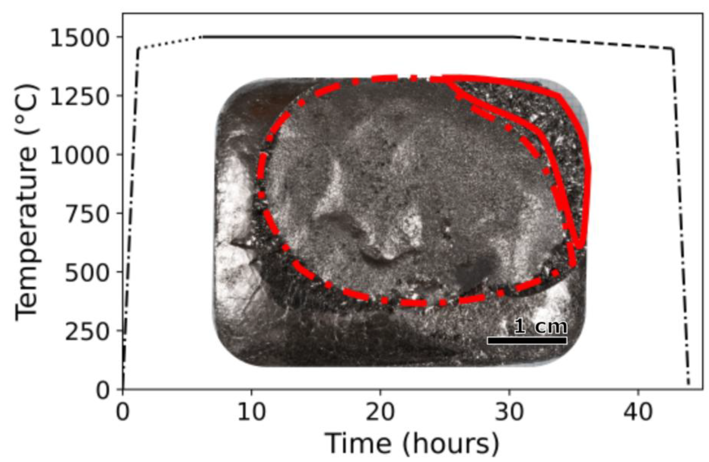
Figure 2.
(a) Exfoliated 13C graphite crystal flake grown under the following conditions: 5.8 carbon-13 wt. %, nitrogen gas, and a 1500 °C dwell temperature, (b) surface image of same crystal. (c) Demonstration of grain counting and measuring on natural carbon equivalent to (a) with (d) surface texture image. White arrows point at steppes, yellow arrows at defects, red arrows at grain boundaries, and black arrows at folds visible on the surface.
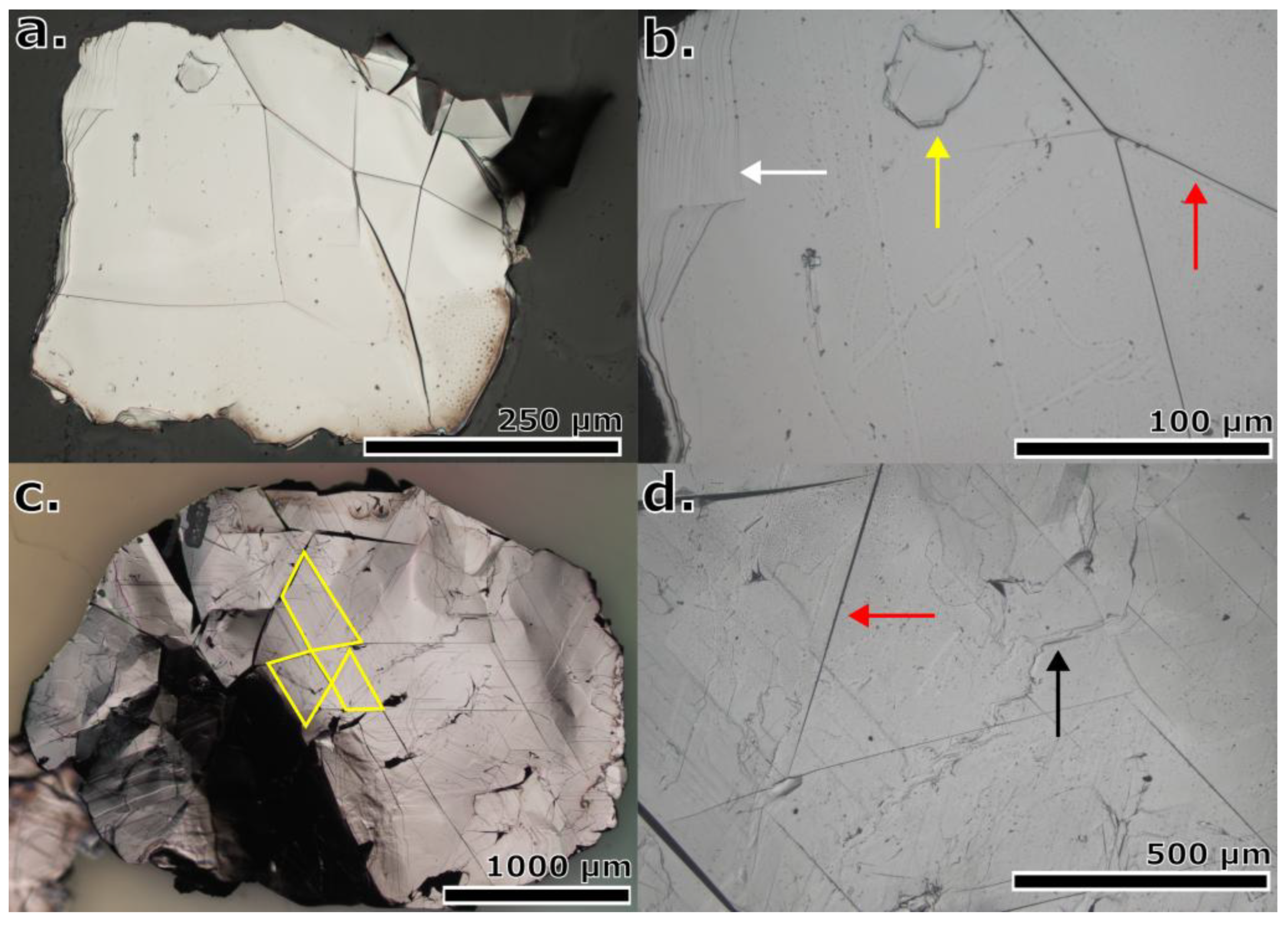
Figure 3.
Drawing of typical topology of graphite etch pits (a) flat-bottomed pits with (c) cross-sectional view and (b) pointed-bottom pits with (d) cross-sectional view.
Figure 3.
Drawing of typical topology of graphite etch pits (a) flat-bottomed pits with (c) cross-sectional view and (b) pointed-bottom pits with (d) cross-sectional view.
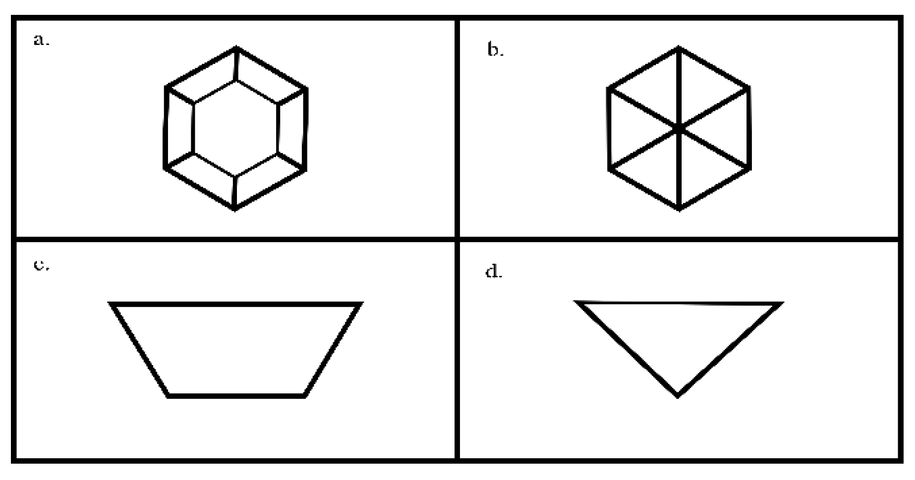
Figure 4.
Box plots of average graphite crystal grain size versus (a) carbon wt. %, (b) cover gas, (c) and maximum dwell temperature with corresponding temperature schedules (right).
Figure 4.
Box plots of average graphite crystal grain size versus (a) carbon wt. %, (b) cover gas, (c) and maximum dwell temperature with corresponding temperature schedules (right).
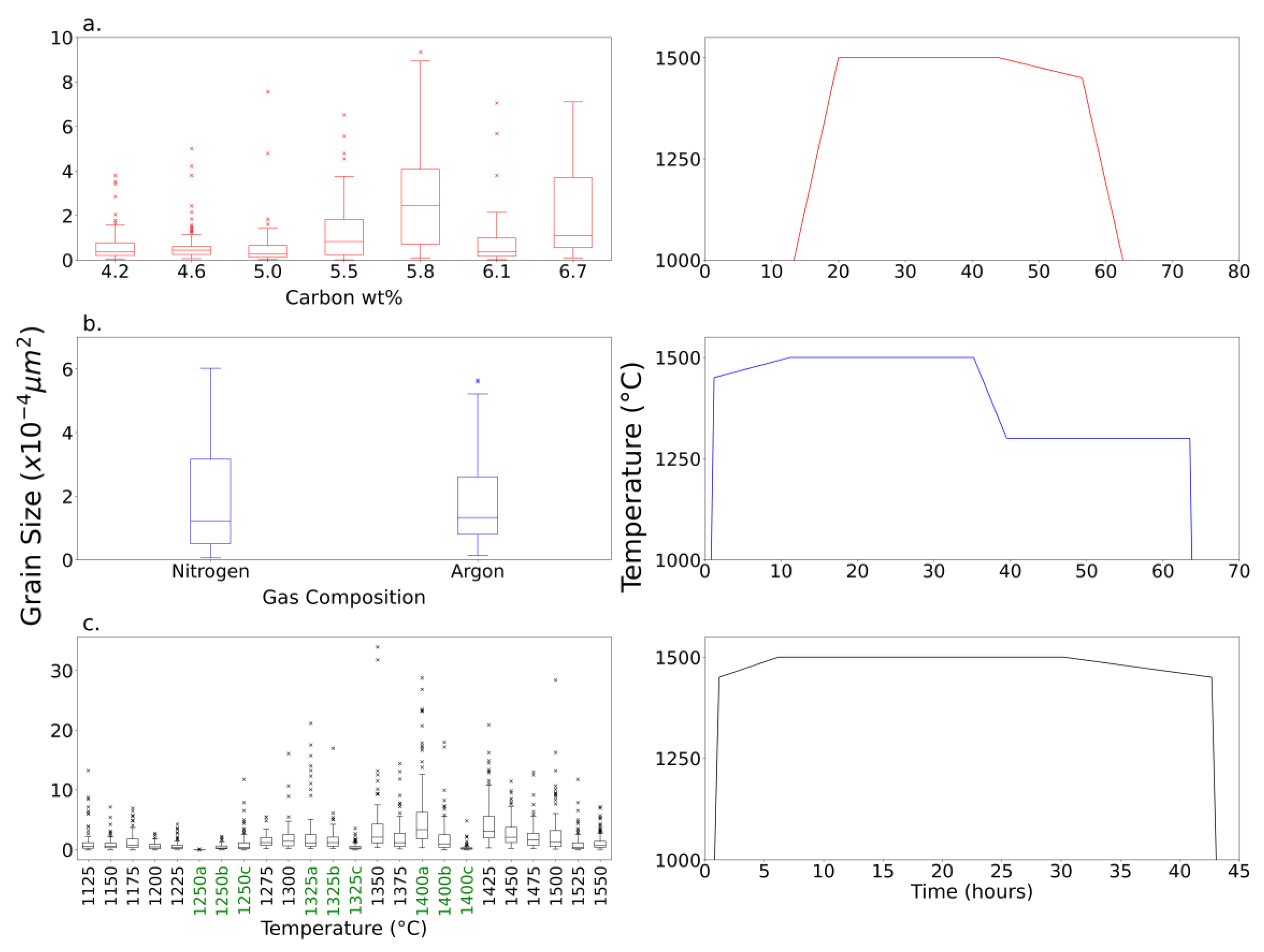
Figure 5.
(a) Raman spectra of isotopically enriched graphite of different isotopic purities. (b) G-peak FWHM as a function of isotope concentration. (c) G-peak shift as a function of isotopic purity.
Figure 5.
(a) Raman spectra of isotopically enriched graphite of different isotopic purities. (b) G-peak FWHM as a function of isotope concentration. (c) G-peak shift as a function of isotopic purity.
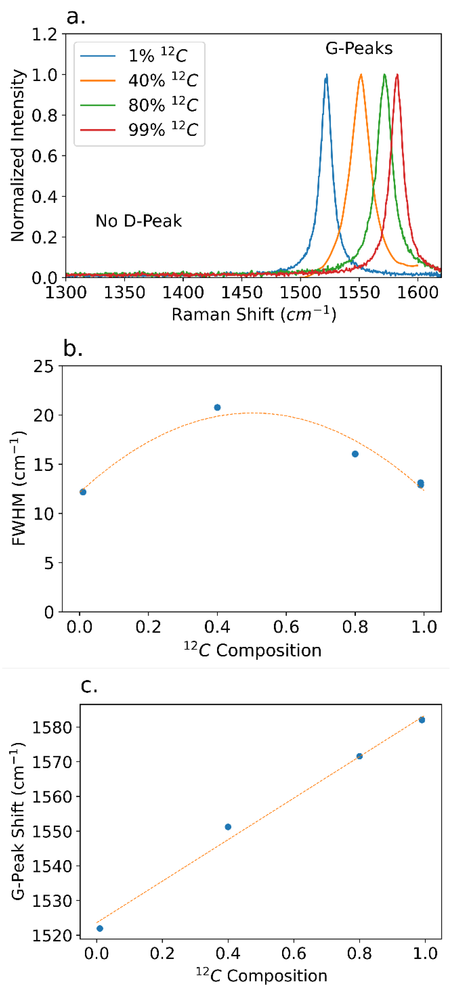
Figure 6.
Histograms of the G-peak FWHM of 960 measurements mapped across (a) 1% 12C, (b) 80% 12C, and (c) 99% 12C graphite single crystals.
Figure 6.
Histograms of the G-peak FWHM of 960 measurements mapped across (a) 1% 12C, (b) 80% 12C, and (c) 99% 12C graphite single crystals.
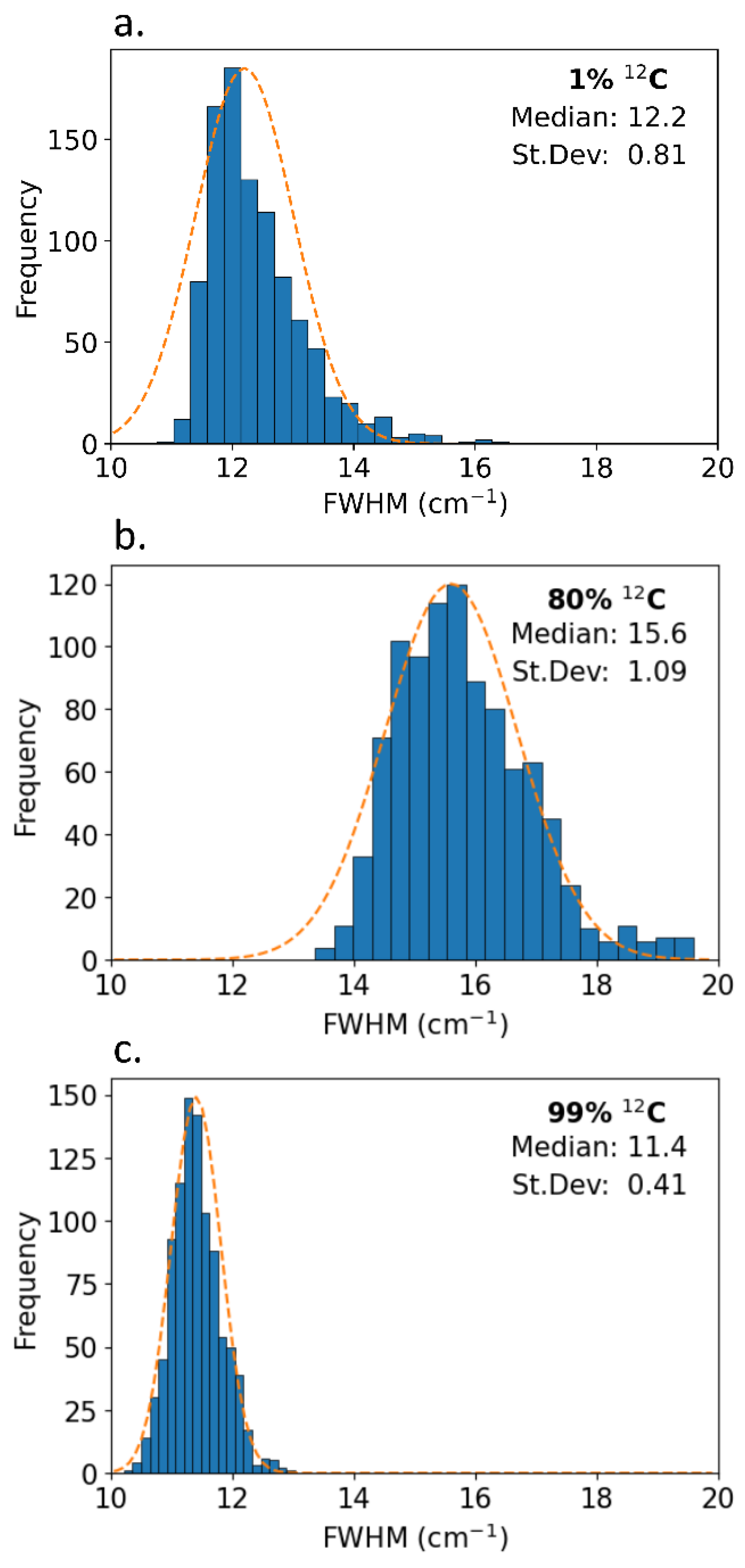
Figure 7.
(a) XRD 002 Peak FWHM versus carbon composition and (b) normalized sample XRD pattern of 6.1 wt. %.
Figure 7.
(a) XRD 002 Peak FWHM versus carbon composition and (b) normalized sample XRD pattern of 6.1 wt. %.
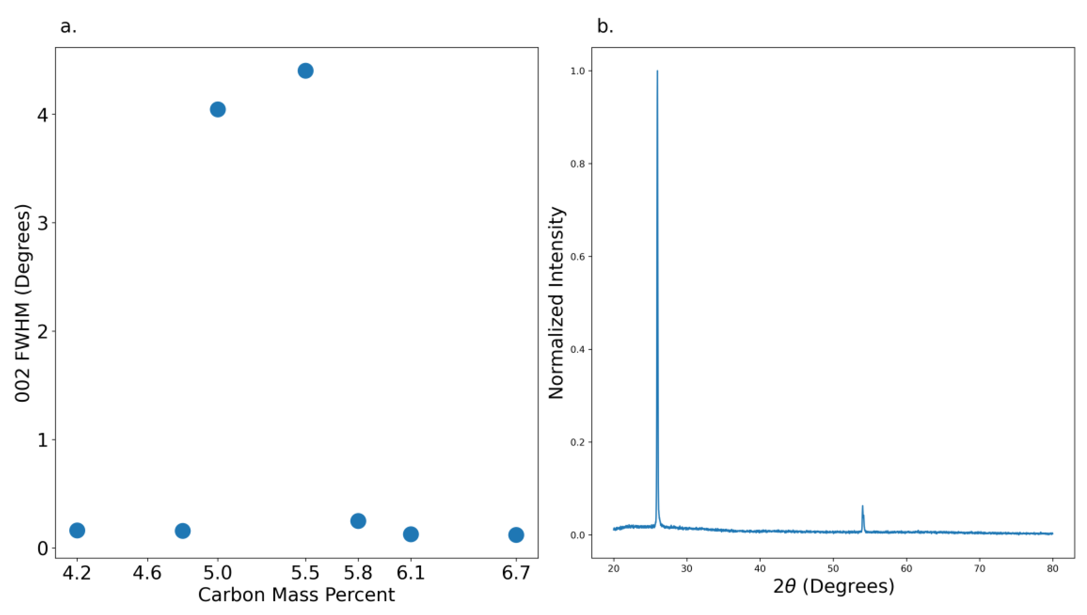
Figure 8.
(a) Etch pits on graphite crystal at 1000x magnification(b) Etch pits in the shape of hexagons with flat (dashed box) and pointed bases (dotted box) captured in SEM. (b) SEM image of flat DSE etch pits and (c) pointed etch pits. Scale bars are (a) 10 µm (b) 300 nm and (c, d)100 nm.
Figure 8.
(a) Etch pits on graphite crystal at 1000x magnification(b) Etch pits in the shape of hexagons with flat (dashed box) and pointed bases (dotted box) captured in SEM. (b) SEM image of flat DSE etch pits and (c) pointed etch pits. Scale bars are (a) 10 µm (b) 300 nm and (c, d)100 nm.
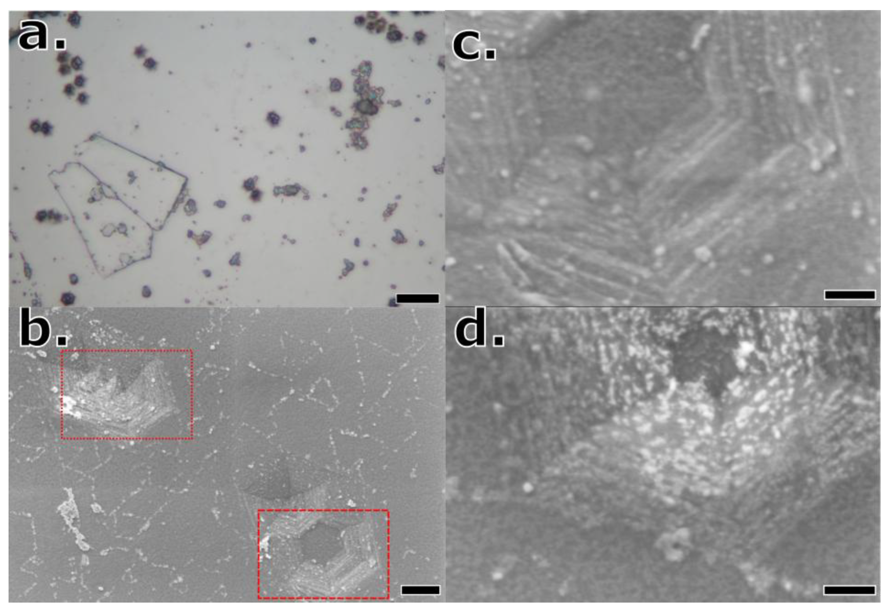
Figure 9.
Effects of (a) initial carbon weight %, (b, c) cover gas composition, and (d) maximum process temperature on dislocation frequency per unit area (left y-axis, blue circles), pit area (right y-axis, orange squares) of individual samples.
Figure 9.
Effects of (a) initial carbon weight %, (b, c) cover gas composition, and (d) maximum process temperature on dislocation frequency per unit area (left y-axis, blue circles), pit area (right y-axis, orange squares) of individual samples.
Disclaimer/Publisher’s Note: The statements, opinions and data contained in all publications are solely those of the individual author(s) and contributor(s) and not of MDPI and/or the editor(s). MDPI and/or the editor(s) disclaim responsibility for any injury to people or property resulting from any ideas, methods, instructions or products referred to in the content. |
© 2026 by the authors. Licensee MDPI, Basel, Switzerland. This article is an open access article distributed under the terms and conditions of the Creative Commons Attribution (CC BY) license (http://creativecommons.org/licenses/by/4.0/).
Copyright: This open access article is published under a Creative Commons CC BY 4.0 license, which permit the free download, distribution, and reuse, provided that the author and preprint are cited in any reuse.


