Submitted:
12 February 2026
Posted:
13 February 2026
You are already at the latest version
Abstract
This work presents an extensive investigation on the synthesis, structural characterization, optical evaluation, and device applications of Er-doped and Er-Yb co-doped ZnO thin films prepared via a citric acid-assisted sol-gel process combined with spin coating. Pd/ZnO:Er and (Er/Yb)/n-Si/Au-Sb Schottky barrier diodes were fabricated using resistive evaporation technique for precise contact deposition. The impact of Er and Er-Yb codoping on structural, optical, and electrical properties, as well as device performance was compared in detail, providing insights into rare-earth codoping strategies for high-performance optoelectronic devices. X-ray diffraction (XRD) analysis confirmed the retention of the hexagonal wurtzite structure in all films, with minor shifts in peak positions indicating successful doping. Optical characterization revealed a slight widening of the bandgap in co-doped films, attributed to the dopant effect. Electrical measurements of SBDs demonstrated improved rectification ratios, lower ideality factors, and higher barrier heights in co-doped films compared to undoped Er doped counterparts. These findings underscore the efficacy of Er/Yb co-doping in modulating the properties of ZnO thin films for advanced optoelectronic applications.
Keywords:
Er-doped ZnO
; Er/Yb co-doping
; sol-gel spin coating
; Schottky barrier diode
; thin films
1. Introduction
Zinc oxide (ZnO) thin films are widely recognized for their potential in optoelectronic devices due to their wide bandgap (~3.37 eV), high exciton binding energy (~60 meV), and excellent transparency across the visible spectrum [1,2]. Consequently, these intrinsic properties make ZnO suitable for a range of applications including photodetectors, light-emitting diodes (LEDs), and solar cells [3]. Furthermore, the versatility of ZnO allows for integration with other materials and dopants to tailor its properties for specific device requirements [4].
Incorporating rare-earth ions such as erbium (Er) and ytterbium (Yb) into ZnO modifies its optical behavior. Specifically, erbium introduces characteristic green and red emissions, while ytterbium acts as a sensitizer, enhancing up-conversion luminescence efficiency [5,6]. Moreover, recent investigations suggest that co-doping ZnO with both Er and Yb can produce synergistic effects, resulting in higher luminescent efficiency and extended device functionality [7]. Therefore, understanding the interaction between these dopants and the ZnO lattice is critical for optimizing the optical performance of thin films [8,9].
The sol-gel spin coating technique is favored for thin film fabrication due to its low cost, simplicity, and ability to produce uniform coatings [10]. In addition, this method allows precise control over thickness and chemical composition, enabling the production of high-quality ZnO thin films with tailored properties [1,11,12]. Consequently, sol-gel spin coating has become a widely adopted approach for incorporating rare-earth dopants into ZnO thin films, bridging the gap between material synthesis and device implementation [13].
Device performance is strongly influenced by the choice of metal contacts. Palladium (Pd) is commonly used to form Schottky contacts on ZnO, benefiting from its suitable work function [14,15]. Meanwhile, gold-antimony (AuSb) alloys have been demonstrated as low-resistance ohmic contacts for n-type ZnO, facilitating efficient charge transport [16]. Therefore, the combined optimization of Schottky and ohmic contacts is essential for achieving high-performance optoelectronic devices based on doped ZnO thin films [17].
Although extensive research exists on individual doping of ZnO with Er or Yb, few studies address co-doping and its impact on structural, optical, and electrical properties [6,12,18,19]. For example, Ahmed et al. [20] examined Er and Yb co-doped ZnO thin films using sol-gel spin coating, showing enhanced electrical characteristics; however, the underlying mechanisms and device implications were not fully explored. Consequently, there remains a need to understand how co-doping affects both the microscopic and macroscopic properties of ZnO films [17,21]. Moreover, while sol-gel spin coating is well established, there is limited investigation into innovative sol-gel strategies that ensure uniform rare-earth doping and scalable production [10,22,23,24,25]. D. Tolera et al. [1] proposed an acid-assisted sol-gel approach for stabilizing precursor solutions, improving the homogeneity of Er-ZnO and Yb-ZnO thin films. Nevertheless, their study focused primarily on synthesis rather than in-depth property analysis. Hence, further research is required to link fabrication techniques with the resulting film performance. On other hand, despite prior work on Pd Schottky and AuSb ohmic contacts, research examining their combined effect on devices based on Er-Yb co-doped ZnO is scarce [26]. Elgazzar et al. [27] explored Pd and Sn co-doping in ZnO nanostructures, but the performance of Er-Yb co-doped films with these specific contacts remains largely uninvestigated. Therefore, systematic studies that correlate dopant co-incorporation, contact materials, and device performance are essential [28,29].
This study aims to address the aforementioned gaps by systematically examining the effects of Er and Yb co-doping on ZnO thin films fabricated via sol-gel spin coating. By optimizing processing parameters and thoroughly characterizing the films, we intend to enhance understanding of their luminescent and electrical properties. Moreover, integrating Pd Schottky contacts and AuSb ohmic contacts into these co-doped films is expected to improve device efficiency and reliability [30]. In addition, the insights gained from this work could contribute to the development of advanced optoelectronic devices including LEDs, solar cells, sensors, diodes and photodetectors with enhanced performance and broader applicability [31]. This research tries to addresses existing knowledge gaps for future device engineering based on rare-earth co-doped ZnO thin films.
2. Experimental Details
2.1. Materials and Solution Preparation
High-purity reagents were used to ensure reproducibility and to minimize contamination. Zinc acetate dihydrate (Zn(CH3COO)2·2H2O) served as the zinc source, while erbium and ytterbium were introduced as their nitrate pentahydrate salts (Er(NO3)3·5H2O and Yb(NO3)3·5H2O). Ethanol was used as solvent, and monoethanolamine (MEA) together with citric acid were added as chelating and complexing agents to stabilize the precursor solution. Deionized water was used throughout to avoid ionic impurities.
A 0.5 M zinc acetate stock solution was prepared in 60 mL ethanol. MEA (2 mL) and citric acid were added to control hydrolysis and keep the solution stable. The mixture was magnetically stirred at 60 °C for 2 hours to fully dissolve and homogenize the solution, then left to age at room temperature for 48 hours to promote network formation and improve dopant dispersion. Dopant salts (Er and Yb) were introduced to yield atomic concentrations of 0, 1, 3, and 5 at.% for single (Er) and co-doped (Er–Yb) formulations, with continuous stirring during addition to avoid local aggregation.
2.2. Thin Film Deposition
Microscope glass slides were chosen for structural and optical studies, whereas n-type silicon (n-Si) substrates were reserved for electrical tests and device fabrication. Substrates underwent ultrasonic cleaning in acetone, ethanol, and deionized water and were dried under nitrogen prior to coating. Films were spun at 4000 rpm for 40 s. After each coating step, films were soft-baked at 350 °C for 10 min to drive off solvent and reduce stress. The coating and preheat cycle were repeated three times to build a uniform film of the desired thickness.
The thermal treatment of the sample was done at 500 °C. Here, we annealed the as-deposited films in air at 500 °C for 1 hour to crystallize the ZnO, remove organics, promote grain growth, and reduce defect densities (such as oxygen vacancies) that strongly influence transport and optical behavior.
2.3. Schottky Diode Fabrication
Schottky diodes were fabricated on n-Si substrates by depositing a 100 nm palladium (Pd) Schottky contact featuring a 0.6 mm diameter circular contact area. Rear-side ohmic contacts were formed using a 150 nm AuSb alloy to ensure low-resistance back contact and reliable current collection. This contact scheme was chosen to provide rectifying behavior with minimized contact resistance.
2.4. Characterization Techniques
X-ray diffraction (XRD) measurements were carried out with Cu Kα radiation (λ = 1.5406 Å) over 2θ = 20–80° to determine phase purity, lattice parameters, and crystallite size (Scherrer analysis). These structural metrics are used to correlate doping level with changes in crystallinity and to check for secondary phases.
Transmittance and absorbance measurements were done using UV-Vis spectroscopy in the range of 200–800 nm. Bandgap values were extracted by Tauc-plot analysis to assess how dopants shift the electronic structure and optical absorption edge.
To analyze electrical properties, the I–V curves measurements were performed using an HP 4140B parameter analyzer with applied voltages swept from −2 V to +2 V. The measured I–V data were analyzed using Schottky-diode models to extract barrier height, ideality factor, and leakage currents, which enable direct comparison of device behavior across dopant concentrations.
3. Data Analysis Methods
The XRD analysis was done using lattice spacing (Bragg’s law) and crystallite size (Scherrer equation). The average crystallite size (D) was estimated using the Debye–Scherrer equation given by:
where λ is the X-ray wavelength (1.5406 Å for Cu Kα), β is the full-width at half maximum (FWHM) of the diffraction peak in radians, and θ is the Bragg angle. For crystal spacing (d), Bragg’s law is given by:
The micro-strain (ε) takes the form:
The dislocation density (δ) is:
The lattice parameters are:
The texture coefficient (TC) is given by:
Using standard intensities , , .
UV–Vis spectral analysis was performed with the help of Tauc plots for optical bandgap estimation. The optical bandgap (Eg) was determined using the following Tauc relation:
where α is the absorption coefficient, hν is the photon energy, A is a constant, and Eg is the optical bandgap. Extrapolation of the linear region of vs hν yields the bandgap value.
The I–V curves analysis employed nonlinear regression fits to Schottky diode equations to obtain barrier height and ideality factor. The following equations were used:
where n is the ideality factor, ΦB is the barrier height, A is the effective contact area (2.827 × 10⁻³ cm2), and A* is Richardson’s constant (32 A·cm−2·K−2 for ZnO).
The ideality factor (n) is extracted from the slope of the forward bias region in the semi-log I–V plot via:
The barrier height (ΦB) is calculated from the reverse saturation current Is:
The rectification ratio (RR) is obtained using:
Table 1.
| Parameter | Selected Value | Purpose / Notes |
| Zinc acetate concentration | 0.5 M | Host precursor concentration |
| Solvent volume | 60 mL ethanol | Sol formation and viscosity control |
| Stabilizers | MEA 2 mL, Citric acid | Chelation; stabilizes sol and controls hydrolysis |
| Dopant concentrations | 0, 1, 3, 5 at.% (Er; Er-Yb) | Study of single and co-doping effects |
| Stirring temperature | 60 °C | Promote dissolution and homogenization |
| Stirring time | 2 h | Ensure complete sol formation |
| Aging time | 48 h | Improve precursor stability and homogeneity |
| Spin speed | 4000 rpm | Achieve uniform film thickness |
| Spin time | 40 s | Control film thickness |
| Preheat (soft-bake) | 350 °C, 10 min | Remove solvents between layers |
| Number of coating cycles | 3 | Achieve target thickness and uniformity |
| Annealing | 500 °C, 1 h (air) | Crystallization and removal of organics |
| Schottky contact | Pd, 100 nm, 0.6 mm diameter | Rectifying top contact |
| Ohmic contact | AuSb, 150 nm | Low-resistance back contact |
| Electrical measurement | HP 4140B, -2 to +2 V | Extraction of I-V device |
4. Results and Discussion
This section presents a consolidated analysis of the structural (XRD), optical (UV–Vis), and electrical (Schottky diode) properties of ZnO thin films doped with Er and Er:Yb.
4.1. Structural Analysis (XRD)
Figure 1 and Figure 2 show the X-ray diffraction (XRD) patterns of undoped, Er-doped, and Er/Yb co-doped ZnO thin films. The diffraction peaks in all samples correspond to the hexagonal wurtzite structure of ZnO (JCPDS Card No. 36–1451), confirming that the primary phase remains intact after doping.
4.1.1. Er-Doped ZnO Films
Figure 1 indicates that increasing Er concentration leads to a notable reduction in peak intensity and broadening of diffraction peaks, particularly the (002) reflection. The increase in full-width at half maximum (FWHM) suggests a reduction in crystallite size and deterioration of crystallinity with higher Er content. Additionally, the (002) peak shifts slightly toward lower 2θ values with increasing Er concentration, which is attributed to lattice expansion caused by the substitution of larger Er3+ ions (0.89 Å) for smaller Zn2+ ions (0.74 Å). This substitution induces tensile strain in the ZnO lattice and promotes the formation of lattice defects.
The average crystallite size (D) estimated using the Debye–Scherrer equation decreased progressively from ~22.6 nm for undoped ZnO to ~5.7 nm for 5 at.% Er-doped ZnO. This reduction is mainly due to the strain introduced by larger Er3+ ions, which hinder grain growth. Correspondingly, dislocation density (δ) increased with higher Er doping levels, indicating increased lattice imperfections. The lattice constants (a and c) remained close to the standard values (a ≈ 3.243 Å, c ≈ 5.213 Å), with only minor variations due to Er incorporation (Table 2).
4.1.2. Er/Yb Co-Doped ZnO Films
Figure 2 displays the XRD patterns for Er/Yb co-doped ZnO films. Similar trends were observed, where all peaks remained consistent with the hexagonal wurtzite structure and no secondary phases (e.g., Er2O3 or Yb2O3) were detected. With increasing co-doping concentration, a reduction in peak intensity and an increase in FWHM were recorded. The (002) peak also shifted slightly toward lower 2θ values, indicating lattice distortion due to the substitution of Er3+ (0.89 Å) and Yb3+ (0.87 Å) into Zn2+ sites.
The crystallite size decreased significantly with increasing Er/Yb concentration, from ~17.4 nm in the undoped film to ~5.0 nm at 5 at.% co-doping. This reduction is consistent with the behavior observed in Er-only doped films and confirms that rare-earth ion incorporation restricts crystal growth due to strain effects and ionic radius mismatch. Moreover, dislocation density increased with higher dopant concentration, reflecting increased lattice distortion (Table 2). These structural modifications align with earlier reports where rare-earth doping in ZnO resulted in decreased crystallite size, peak broadening, and shifts due to induced strain and substitutional incorporation [33].
From Table 2, it is observed that (i) Er doping increases strain and lattice disorder, reducing grain size and increasing defect density. (ii) Er/Yb co-doping stabilizes the lattice, leading to relatively larger crystallites and lower strain compared to Er-only doping.
4.2. Optical Analysis (UV–Vis)
The optical transmittance and absorbance spectra of undoped, Er-doped, and Er/Yb co-doped ZnO thin films were recorded in the wavelength range of 350–800 nm, as shown in Figure 3, Figure 4, Figure 5, Figure 6 and Figure 7. All samples exhibited high transparency in the visible region, indicating good optical quality of the thin films.
4.2.1. Er-Doped ZnO Films
Figure 3 shows the transmittance spectra of undoped and Er-doped ZnO thin films. The mean transmittance values showed slight variation with increasing Er concentration: 67.80% (undoped), 67.74% (1 at.% Er), 64.28% (3 at.% Er), and 70.99% (5 at.% Er), as summarized in Table 3. These fluctuations may arise from microstructural differences such as surface roughness, film thickness variation, nano-porosity, and defect density, which can lead to light scattering and interference effects [5].
The absorbance spectra (Figure 4) reveal a sharp absorption edge near the UV region for all samples. A clear blue shift in the absorption edge was observed with increasing Er concentration, suggesting an increase in optical bandgap energy. This behavior can be explained by the Burstein–Moss effect and the quantum confinement effect due to reduced crystallite size [31].
The Tauc plots (Figure 5) were used to estimate the optical bandgap using the direct transition model (Equation 7). The extracted bandgap values increased with Er content, measured at 3.023 eV, 3.040 eV, 3.059 eV, and 3.125 eV for 0, 1, 3, and 5 at.% Er doping, respectively (Table 3). This trend is consistent with previous studies reporting bandgap widening in Er-doped ZnO thin films [5].
4.2.2. Er/Yb Co-Doped ZnO Films
The optical behavior of undoped and Er/Yb co-doped ZnO films was also studied using UV–Vis spectroscopy.
Figure 6 shows the transmittance spectra, which generally exhibit reduced transmittance compared to undoped ZnO. The average transmittance values were 66.99% (undoped), 55.51% (1 at.% co-doped), 63.82% (3 at.%), and 64.25% (5 at.%) (Table 3). The initial reduction in transmittance at 1 at.% may be attributed to enhanced light scattering caused by increased surface roughness, structural imperfections, or the formation of sub-bandgap states due to dopant incorporation [32]. With increasing co-dopant concentration, partial recovery of transmittance suggests improved film quality or better dopant homogenization at higher concentrations.
The absorbance spectra (Figure 7) show a prominent absorption edge around 362 nm for the undoped ZnO film. The absorption edge shifts toward shorter wavelengths (blue shift) with increasing co-dopant concentration, indicating changes in band structure and carrier concentration.
The bandgap energies were obtained from Tauc plots (Figure 8). The calculated bandgap values for undoped, 1 at.%, 3 at.%, and 5 at.% Er/Yb co-doped ZnO films were 3.113 eV, 3.156 eV, 3.195 eV, and 3.214 eV, respectively (Table 3). Unlike the monotonic increase observed in Er-only doped films, the co-doped samples displayed a slight bandgap narrowing at low concentration (1 at.%) followed by broadening at higher concentrations. This behavior can be explained by competing effects of defect-induced band tailing and the Burstein–Moss shift [33].
4.2.3. Bandgap Comparison and Discussion
For undoped ZnO, the bandgap values were ~3.023 eV (Er system) and ~3.113 eV (Er/Yb system). With Er doping, a gradual increase in bandgap was observed due to the Burstein–Moss effect and reduced crystallite size. In contrast, Er/Yb co-doping resulted in a modest blue shift, indicating increased carrier concentration and modified band structure. These trends confirm that rare-earth doping effectively alters the electronic structure and optical transitions in ZnO, in agreement with previous studies on Er/Yb co-doped ZnO systems [34].
4.3. Electrical Properties and Schottky Diode Performance
The current–voltage (I–V) characteristics of Pd/ZnO:RE/n-Si/AuSb Schottky diodes (RE = rare earth) were measured under forward and reverse bias conditions. All devices exhibited rectifying behavior, confirming successful Schottky junction formation.
4.3.1. Er-Doped ZnO Schottky Diodes
The room-temperature semi-logarithmic I–V characteristics of Schottky diodes fabricated on undoped and Er-doped ZnO films are presented in Figure 9. A clear improvement in the forward/reverse current ratio was observed for Er-doped devices compared to the undoped reference.
In the low forward bias region (V < 0.4 V), diodes fabricated on undoped (0 at.% Er) and 3 at.% Er films display generation–recombination current mechanisms, whereas thermionic emission dominates at higher bias (Equation 8). In contrast, devices fabricated on 1 at.% and 5 at.% Er films follow a pure thermionic-emission behavior across the entire forward-bias range. Deviations from linearity at V > 0.7 V are attributed to series resistance effects [35]. Additionally, the reverse leakage current is significantly reduced in all Er-doped devices compared to the undoped sample, indicating improved barrier quality.
Schottky barrier height (ΦB) and ideality factor (n) were extracted from the linear region of the forward semi-log I–V curve using thermionic emission fitting (Figure 10).
The undoped diode exhibited Φb ≈ 0.655 eV and n ≈ 4.77, whereas Er-doped devices showed enhanced barrier heights of 0.674 eV (1 at.%), 0.761 eV (3 at.%), and 0.789 eV (5 at.%), with a corresponding decrease in ideality factor (Table 4). Ideality factors greater than unity are attributed to carrier recombination in the space-charge region, barrier height inhomogeneity, and series resistance effects [21].
4.3.2. Er/Yb Co-Doped ZnO Schottky Diodes
Figure 11 shows the semi-log I–V curves for Schottky diodes on undoped and Er/Yb co-doped ZnO films.
All co-doped devices demonstrate good rectification, with the 3 at.% (Er, Yb) sample showing the highest forward/reverse ratio. Devices on undoped (0 at.%) and 1 at.% co-doped films exhibit generation–recombination mechanisms at low bias, transitioning to thermionic emission at higher bias (Equation 8). For 3 at.% and 5 at.% co-doped devices, thermionic emission is dominant across the forward-bias range, with deviations at V > 0.8 V due to series resistance. The reverse leakage current is significantly lower in co-doped devices compared to undoped. The extracted ΦB and n values are listed in Table 5. Barrier heights increased from 0.595 eV (undoped) to 0.758 eV (1 at.%), 0.771 eV (3 at.%), and 0.743 eV (5 at.%) upon co-doping.
4.3.3. Discussion of Electrical Performance
The results indicate that Er doping increases barrier height and reduces ideality factor, which is consistent with reduced leakage and improved junction quality. Co-doping with Er/Yb further enhances diode performance, producing higher barrier heights, lower ideality factors, and improved rectification ratios compared to Er-only doped devices. This behavior suggests synergistic effects in passivating defects, improving interface quality, and enhancing charge transport.
Both Er and Er/Yb doped devices show a transition from highly non-ideal behavior (n ≫ 1) toward near-thermionic emission behavior (n ≈ 1.13–1.38) with increasing dopant concentration. Er/Yb devices consistently show lower ideality factors at matched doping levels, indicating cleaner interfaces and reduced defect-assisted transport. The saturation current (Is) decreases by several orders of magnitude from undoped to doped samples, consistent with reduced thermally activated leakage and improved barrier integrity.
The reverse leakage current at −1.0 V decreases dramatically with doping, especially at 3 at.%, producing rectification ratios greater than 105 for the best devices. The enhanced performance of Er/Yb co-doped diodes highlights the benefits of co-doping in improving structural, optical, and electrical properties simultaneously, supporting potential applications in UV photodetectors, upconversion-based photonic devices, transparent electronics, and energy conversion systems.
5. Conclusion
Er-doped and Er/Yb co-doped ZnO thin films were successfully synthesized using a citric acid–assisted sol–gel spin coating technique. Structural characterization confirmed the retention of the hexagonal wurtzite ZnO phase, with no secondary phases detected. Er and Er/Yb incorporation led to grain size reduction, peak broadening, and lattice distortion due to the substitution of larger rare-earth ions into Zn sites. Co-doping with Yb improved crystallinity and reduced lattice strain compared to single Er doping.
Optical analysis revealed that all films maintained high transparency in the visible region. The optical bandgap exhibited a blue shift with increasing dopant concentration, attributed to the Burstein–Moss effect and quantum confinement in nanostructured films. Er/Yb co-doping produced a higher bandgap shift and enhanced optical response compared to Er-only doping.
Electrical characterization of Pd/ZnO:RE/n-Si/AuSb Schottky diodes demonstrated clear rectifying behavior in all devices. Both Er and Er/Yb doping improved the Schottky barrier height and reduced the ideality factor, indicating enhanced interface quality and reduced recombination. The best performance was achieved at 3 at.% co-doping, where the device showed the highest barrier height, lowest leakage current, and a rectification ratio exceeding 105. Overall, Er/Yb co-doped films exhibited superior electrical performance compared to Er-only doped films.
The results confirm that Er/Yb co-doping is an effective strategy for tailoring the structural, optical, and electrical properties of ZnO thin films. These findings highlight the potential of co-doped ZnO films for high-performance Schottky barrier diodes, UV photodetectors, and other transparent optoelectronic devices.
Author Contributions
Conceptualization: Dechasa Tolera and Teshome Senbeta; methodology: Dechasa Tolera; formal analysis: Dechasa Tolera; investigation: Dechasa Tolera; writing original draft preparation: Dechasa Tolera; writing review and editing: Dechasa Tolera, Teshome Senbeta and Belayneh Mesfin; supervision: Teshome Senbeta and Belayneh Mesfin. All authors have read and agreed to the published version of the manuscript.
Data Availability Statement
The data presented in this study are available on request from the corresponding author. The data are not publicly available due to ongoing research and data reuse considerations.
Acknowledgments
The authors thank colleagues and Department of physics laboratory staff, and department of materials science and engineering (ASTU, Adama) for their assistance with experimental setup and data acquisition, and for providing access to the characterization equipment facility. The authors also acknowledge the support from MoE for Funding.
Conflicts of Interest
The authors declare no conflicts of interest. The funders had no role in the design of the study; in the collection, analyses, or interpretation of data; in the writing of the manuscript; or in the decision to publish the results.
References
- Tolera, D.; Senbeta, T.S.; Mesfin, B. Optical and temperature dependent electrical properties of Er-/Yb-doped ZnO Schottky diodes and thin films. Sci. Rep. 2025, 15, 1320. [Google Scholar] [CrossRef]
- Zheng, B.; et al. Rare-Earth Doping in Nanostructured Inorganic Materials. Chem. Rev. 2022, 122, 5519–5603. [Google Scholar] [CrossRef]
- Sharma, D.K.; et al. A review on ZnO: Fundamental properties and application. Mater. Today Proc. 2022, 49, 3028–3035. [Google Scholar] [CrossRef]
- Lopez-Mena, E.R.; et al. The effect of Yb doping on the ZnO thin films obtained via a low temperature spin coating method. J. Mater. Sci.: Mater. Electron. 2021, 31, 1–? (article number not provided). [Google Scholar] [CrossRef]
- Murali, K.R.; Subasri, R.; Vijila, M. Enhanced photoluminescence and electrical properties of Er-doped ZnO thin films. Mater. Sci. Semicond. Process. 2014, 18, 97–104. [Google Scholar] [CrossRef]
- Ahmed, M.A.M.; Ahmed, M.E.I. Structural, optical and electrical properties of the fabricated Schottky diodes based on ZnO, Ce and Sm doped and co-doped ZnO films prepared via wet chemical technique. Mater. Sci. Semicond. Process. 2023, 132, 105975. [Google Scholar] [CrossRef]
- Pearton, S.J.; et al. ZnO electronics for UV detection. J. Appl. Phys. 2003, 93, 1–13. [Google Scholar] [CrossRef]
- Ding, J.; Chen, H.; Fu, H. Defect-related photoluminescence emission from annealed ZnO films deposited on AlN substrates. Mater. Res. Bull. 2017, 95, 185–189. [Google Scholar] [CrossRef]
- Jalali, A.; et al. Synthesis of Zinc oxide thin films by sol-gel method and applications to improve the efficiency of silicon solar cells. Chem. Methodol. 2020, 15, 343–356. [Google Scholar] [CrossRef]
- Mouet, T.; et al. Growth and characterization of thin ZnO films deposited on glass substrates by electrodeposition techniques. Appl. Surf. Sci. 2010, 256, 4114–4120. [Google Scholar] [CrossRef]
- Sood, S.; et al. Enhancing Optoelectronic performance through rare-earth doped ZnO: Insights and applications. Photonics 2025, 12, 5454. [Google Scholar] [CrossRef]
- Periyasamy, A.P.; et al. Progress in Sol-Gel Technology for the Coatings of Fabrics. Materials 2020, 13, 1838. [Google Scholar] [CrossRef]
- Ahzan, et al. Synthesis and Characterization of ZnO Thin Layers using Sol-Gel Spin coating method. J. Penelit. Pengkaj. Ilmu Pendidik. 2021, 182–194. [Google Scholar] [CrossRef]
- Asghar, M.; et al. Electrical characterizations of Au/ZnO/Si Schottky contacts. J. Phys.: Conf. Ser. 2013, 439, 012030. [Google Scholar] [CrossRef]
- Tan, S.T.; et al. High-performance Pd/ZnO Schottky diodes. J. Appl. Phys. 2005, 98, 014502. [Google Scholar] [CrossRef]
- Chen, L.F.; et al. Formation of low-resistance AuSb ohmic contacts to n-type Si. IEEE Electron Device Lett. 1990, 11, 462–464. [Google Scholar] [CrossRef]
- Caglar, Y. Effects of rare earth doping on ZnO nanostructures. J. Alloys Compd. 2014, 617, 595–601. [Google Scholar] [CrossRef]
- Sira, K.; et al. Microstructure and optical properties of rare-earth doped ZnO thin films. Mater. Today Proc., 2015. [Google Scholar] [CrossRef]
- Wang, C.; et al. Metal oxide gas sensors: sensitivity and influencing factors. Sensors 2010, 10, 2088–2106. [Google Scholar] [CrossRef] [PubMed]
- Ip, K.P.; Heo, Y.W.; Baik, K.; Norton, D.P. Temperature-dependent characteristics of Pt Schottky contacts doped on n-type ZnO. Appl. Phys. Lett. 2004, 84, 2835–2837. [Google Scholar] [CrossRef]
- Sharma, A.; et al. Citric acid assisted sol–gel synthesis of ZnO for improved optoelectronic properties. J. Sol-Gel Sci. Technol. 2017, 81, 181–188. [Google Scholar] [CrossRef]
- Ghanem, M.G.; et al. Synthesis and characterization of undoped and Er-doped ZnO nano-structure thin films deposited by sol-gel spin coating technique. Mater. Res. Express 2019, 6, 085916. [Google Scholar] [CrossRef]
- Klingshirn, C. ZnO: From basics towards applications. Phys. Status Solidi B 2007, 244, 3027–3073. [Google Scholar] [CrossRef]
- Zamiri, R.; et al. Effects of rare earth (Er, La and Yb) Doping on morphology and structure Properties of ZnO Nanostructures prepared by wet chemical method. Ceram. Int. 2014, 40, 523–529. [Google Scholar] [CrossRef]
- Elgazzar, A.; et al. Impact of Pd and Sn Co-Doping ZnO Nanoflakes toward high performing Schottky Diodes based on the generation of intermediate bands within the energy gap. Mater. Sci.: Mater. Electron. 2024, 35, 13398–3. [Google Scholar] [CrossRef]
- Ye, Z.; et al. Co-Doping: an effective strategy for achieving stable p-type ZnO thin films. Nano Energy 2018, 52, 527–540. [Google Scholar] [CrossRef]
- Brillson, L.; Lu, Y. ZnO Schottky barriers and Ohmic Contacts. Appl. Phys. Rev. 2011, 109, 121301. [Google Scholar] [CrossRef]
- Ipek, Y.; et al. Rare earth element doped ZnO thin films and Applications. Int. J. Pure Appl. Phys. 2021, 7, 305–313. [Google Scholar] [CrossRef]
- Shen, M.; et al. Optimization of Copper Schottky Contacts on nanocrystalline ZnO thin films by atomic layer deposition. MRS Adv. 2016, 1, 3421–3427. [Google Scholar] [CrossRef]
- Mi, W.; et al. Study of the metal-semiconductor contact to ZnO films. Vacuum 2018, 155, 210–213. [Google Scholar] [CrossRef]
- Reisfeld, R.; Saraidarov, T. Innovative Materials based on sol gel technology. Opt. Mater. 2006, 28, 64–70. [Google Scholar] [CrossRef]
- Gartner, M.; et al. Towards advanced materials: Functional perspectives of co-doped ZnO thin films. Micromachines 2025, 16, 1179. [Google Scholar] [CrossRef] [PubMed]
- Ali, G.M.; et al. Interface properties and junction behavior of Pd contact on ZnO thin film grown by vacuum deposition technique. Phys. Status Solidi C 2010, 7, 252–255. [Google Scholar] [CrossRef]
- Boukhari, A.; et al. Thickness effect on the properties of 4% Mn-doped ZnO thin films grown by sol gel spin coating deposition. Macromol. Symp. 2021, 397, 1. [Google Scholar] [CrossRef]
- Mahalakshmi, S.; et al. Ytterbium-doped ZnO thin films for visible light photocatalysis. Ceram. Int. 2018, 44, 7777–7783. [Google Scholar] [CrossRef]
- Tsiarapas, C.; Girginoudi, D.; Nikolaos, N. Electrical characteristics of Pd Schottky contacts on ZnO thin films. Mater. Sci. Semicond. Process. 2014, 17, 199–206. [Google Scholar] [CrossRef]
- EI Hat, A.; et al. Growth and properties of (Yb-Er) Co-Doped ZnO thin films deposited via spray pyrolysis technique. Optics 2025, 6, 14. [Google Scholar] [CrossRef]
Figure 1.
XRD patterns of undoped and Er-doped ZnO thin films, showing the characteristic hexagonal wurtzite structure. Peak broadening and intensity reduction indicate decreasing crystallite size with higher Er content.
Figure 1.
XRD patterns of undoped and Er-doped ZnO thin films, showing the characteristic hexagonal wurtzite structure. Peak broadening and intensity reduction indicate decreasing crystallite size with higher Er content.
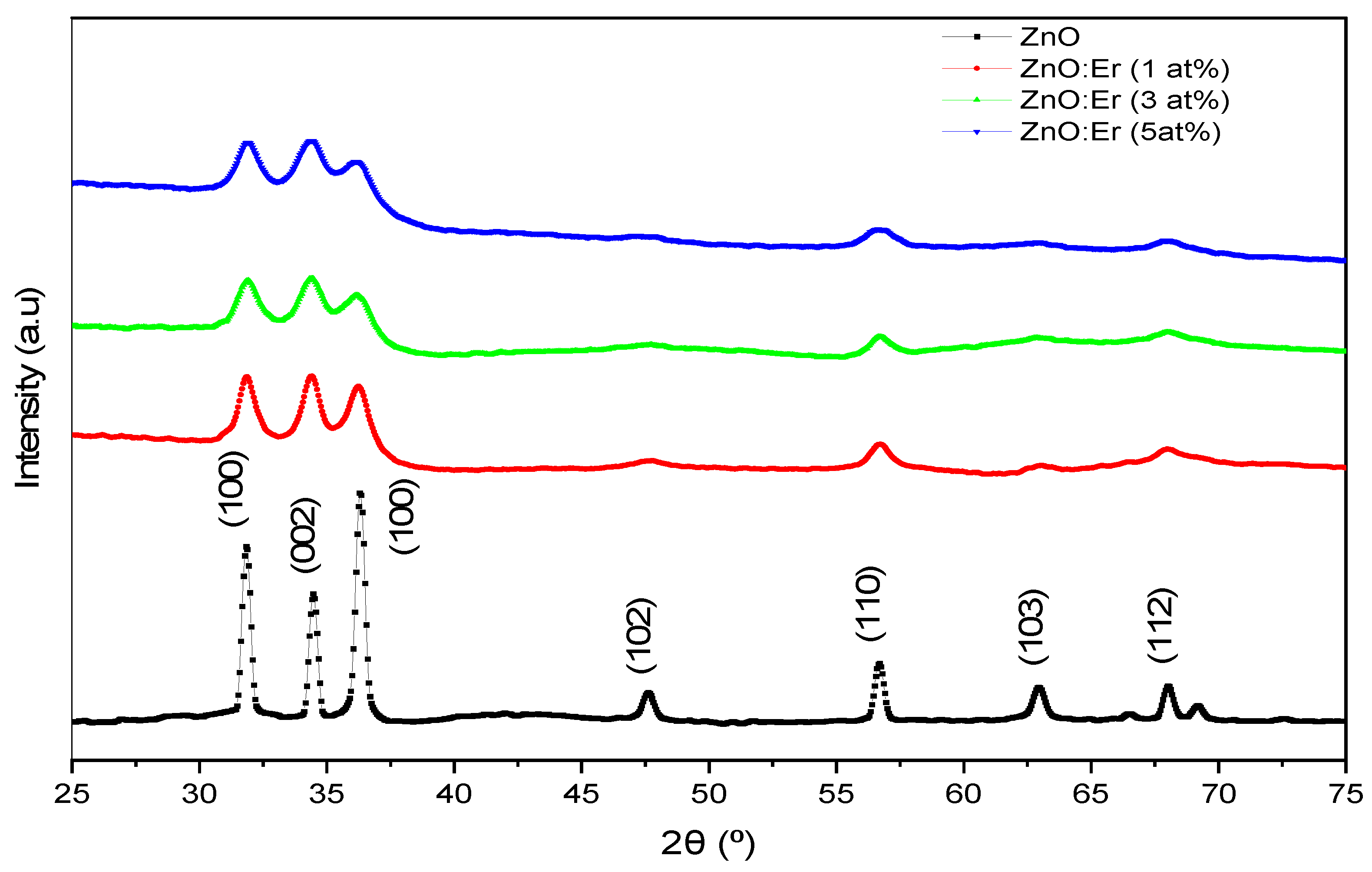
Figure 2.
XRD patterns of undoped and (Er, Yb)-co-doped ZnO thin films. All diffraction peaks correspond to the hexagonal wurtzite phase. Peak shifts and broadening reflect lattice distortion caused by co-doping.
Figure 2.
XRD patterns of undoped and (Er, Yb)-co-doped ZnO thin films. All diffraction peaks correspond to the hexagonal wurtzite phase. Peak shifts and broadening reflect lattice distortion caused by co-doping.
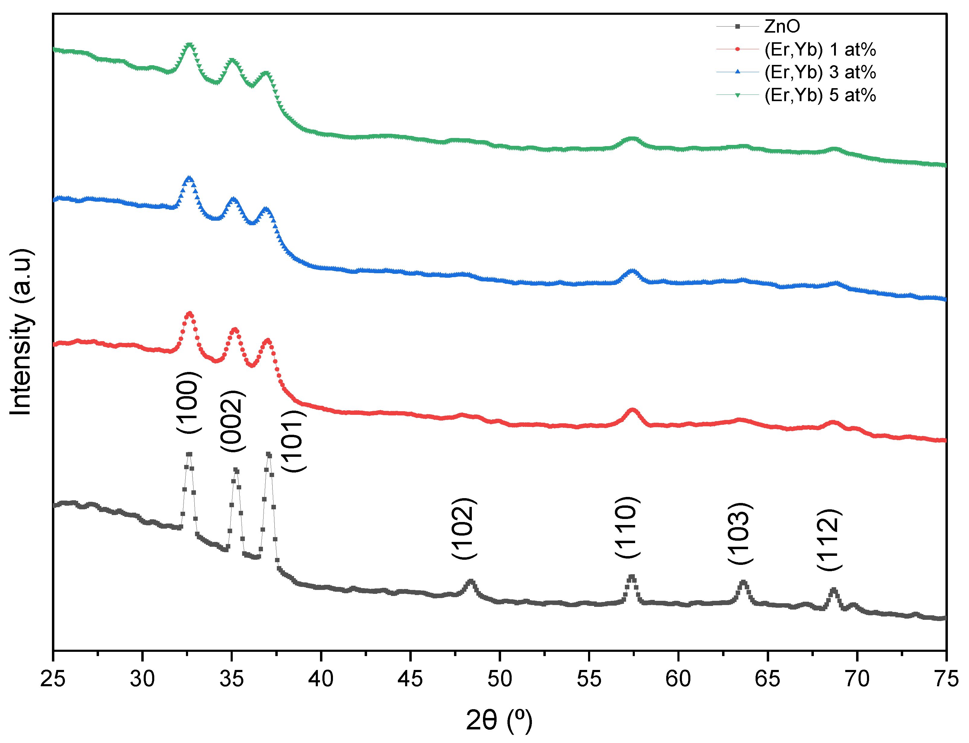
Figure 3.
UV-Vis transmittance spectra of undoped and Er-doped ZnO thin films. High visible transmittance is maintained with minor variations depending on Er concentration.
Figure 3.
UV-Vis transmittance spectra of undoped and Er-doped ZnO thin films. High visible transmittance is maintained with minor variations depending on Er concentration.
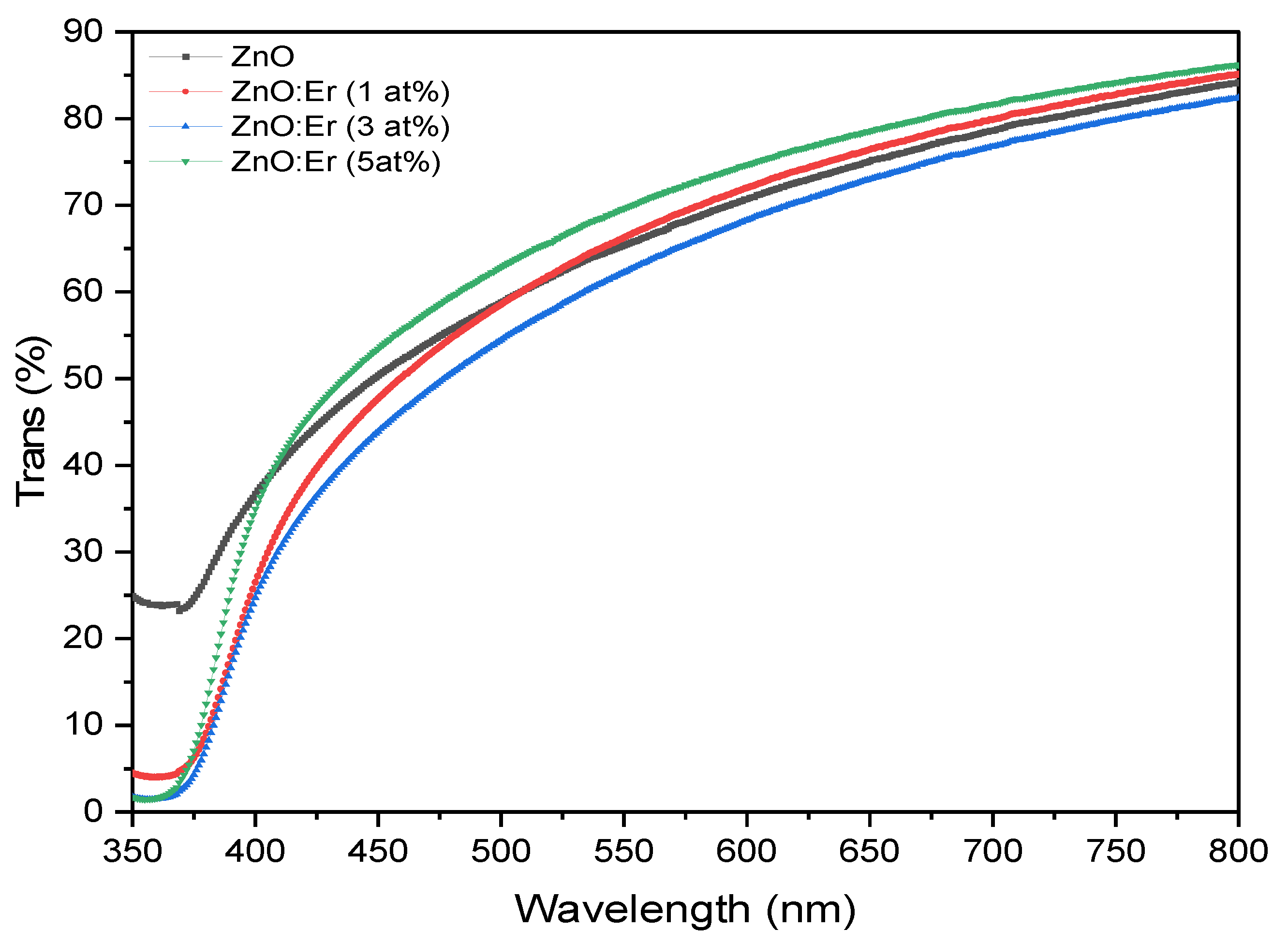
Figure 4.
UV-Vis absorbance spectra of undoped and Er-doped ZnO films, displaying a sharp absorption edge in the UV region. The blue shift with increased Er content indicates bandgap widening.
Figure 4.
UV-Vis absorbance spectra of undoped and Er-doped ZnO films, displaying a sharp absorption edge in the UV region. The blue shift with increased Er content indicates bandgap widening.
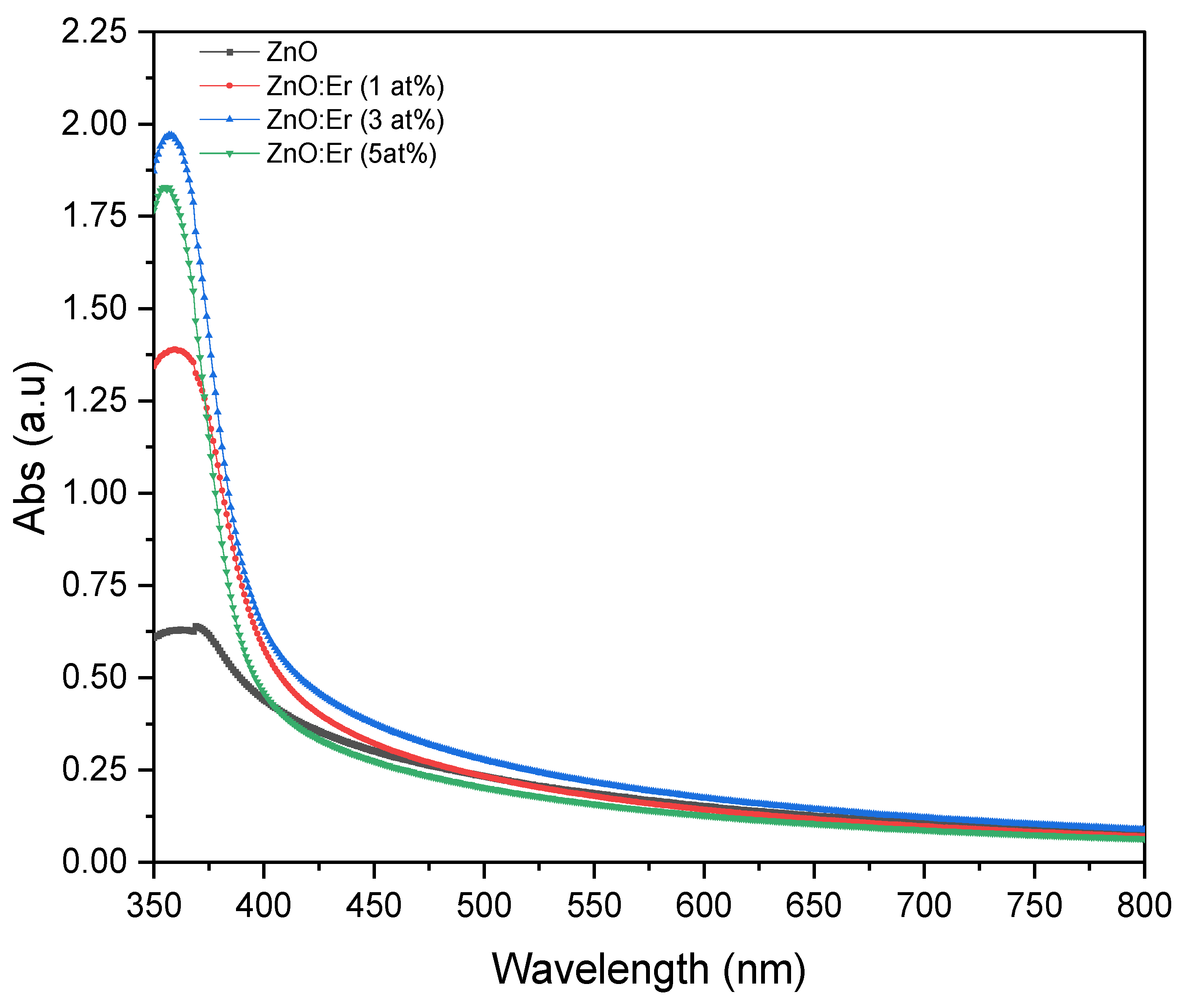
Figure 5.
Tauc plots for Er-doped ZnO films. The linear extrapolation of (αhv)2 versus hv allows estimation of the optical bandgap, showing an increase with Er doping.
Figure 5.
Tauc plots for Er-doped ZnO films. The linear extrapolation of (αhv)2 versus hv allows estimation of the optical bandgap, showing an increase with Er doping.
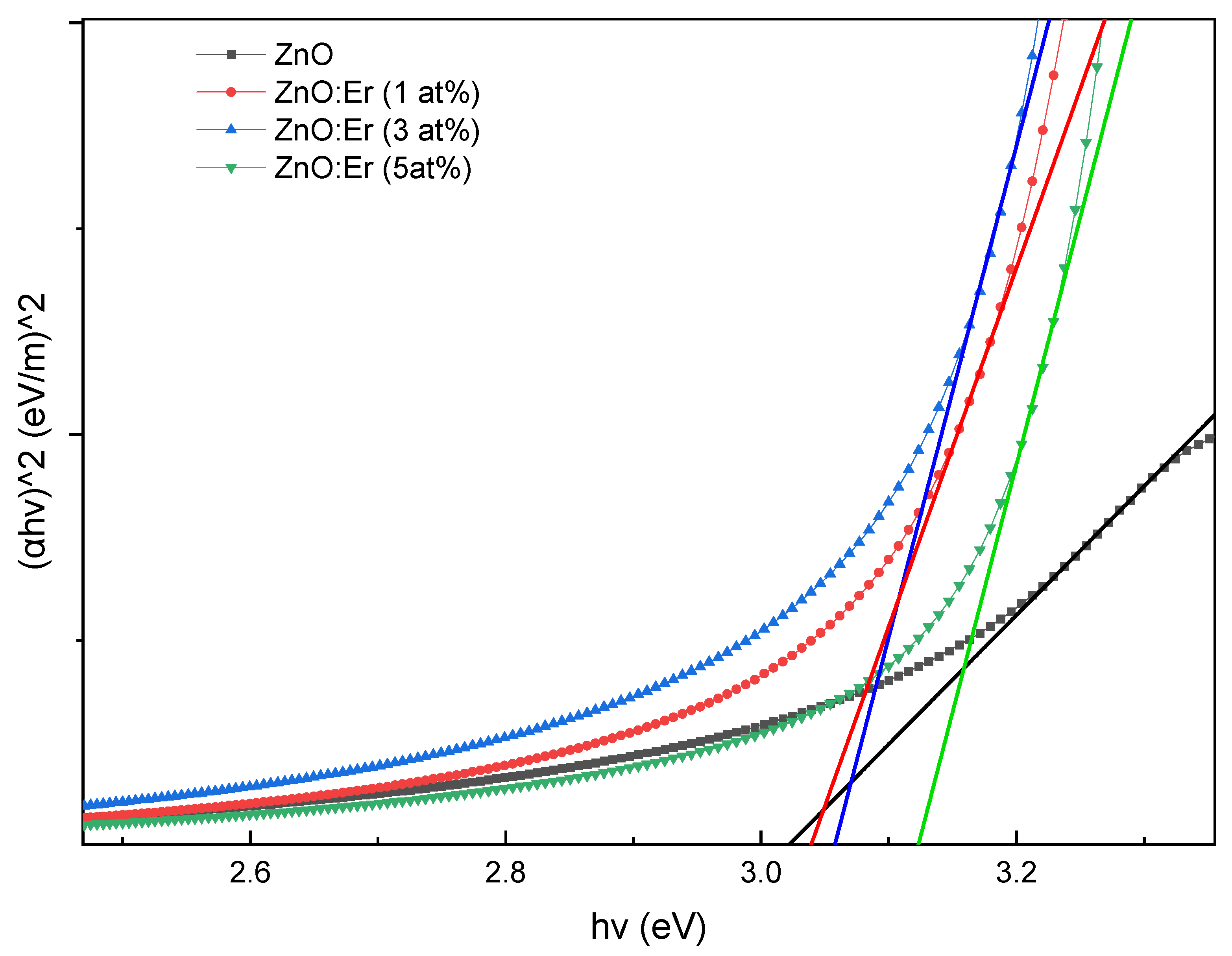
Figure 6.
UV-Vis transmittance spectra of undoped and (Er, Yb)-co-doped ZnO thin films. Transmittance decreases at low co-doping levels but partially recovers at higher concentrations.
Figure 6.
UV-Vis transmittance spectra of undoped and (Er, Yb)-co-doped ZnO thin films. Transmittance decreases at low co-doping levels but partially recovers at higher concentrations.
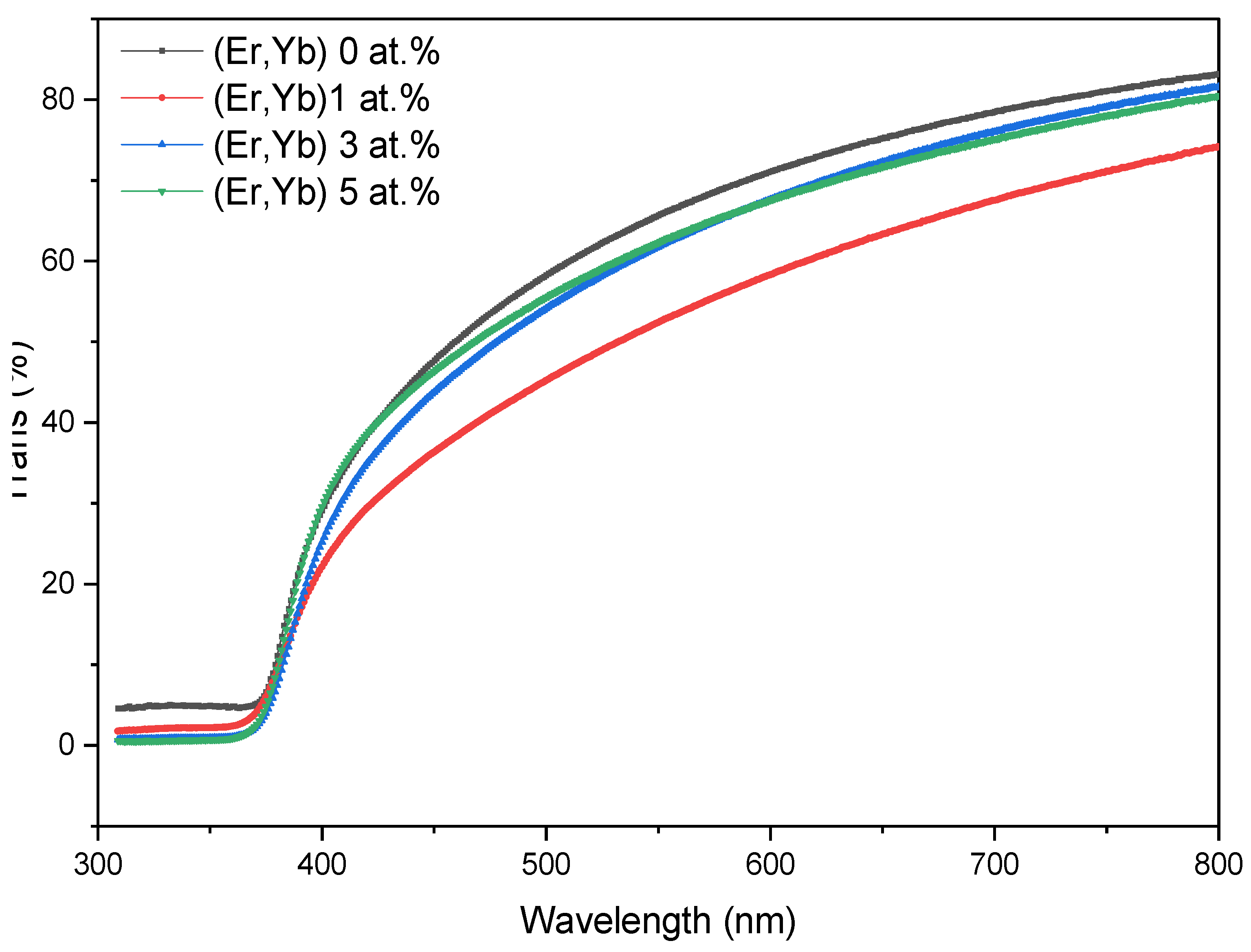
Figure 7.
UV-Vis absorbance spectra of undoped and (Er, Yb) co-doped ZnO films, displaying a sharp absorption edge in the UV region. The blue shift with increased Er content indicates bandgap widening.
Figure 7.
UV-Vis absorbance spectra of undoped and (Er, Yb) co-doped ZnO films, displaying a sharp absorption edge in the UV region. The blue shift with increased Er content indicates bandgap widening.
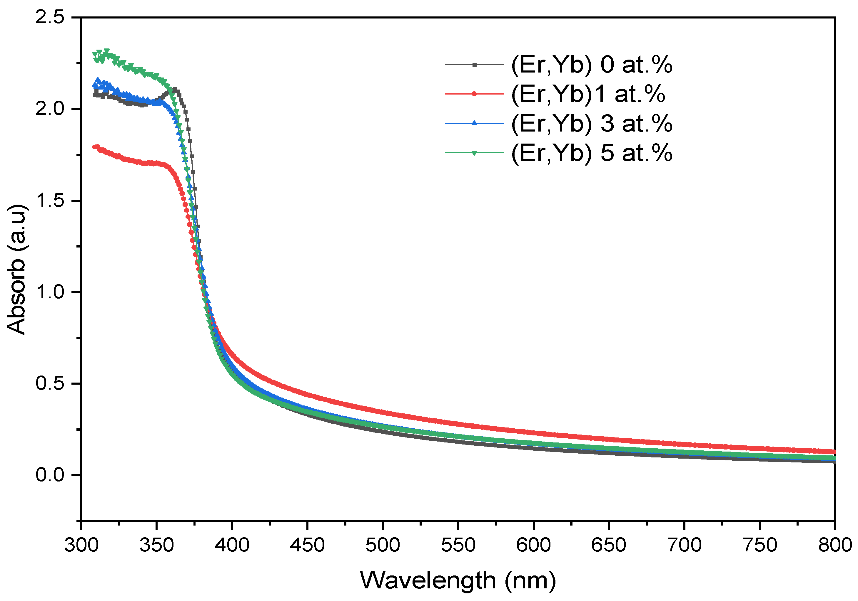
Figure 8.
Tauc plots for (Er, Yb)-co-doped ZnO films. Bandgap energies slightly widen at higher co-doping levels due to a combination of defect effects and Burstein-Moss shift.
Figure 8.
Tauc plots for (Er, Yb)-co-doped ZnO films. Bandgap energies slightly widen at higher co-doping levels due to a combination of defect effects and Burstein-Moss shift.
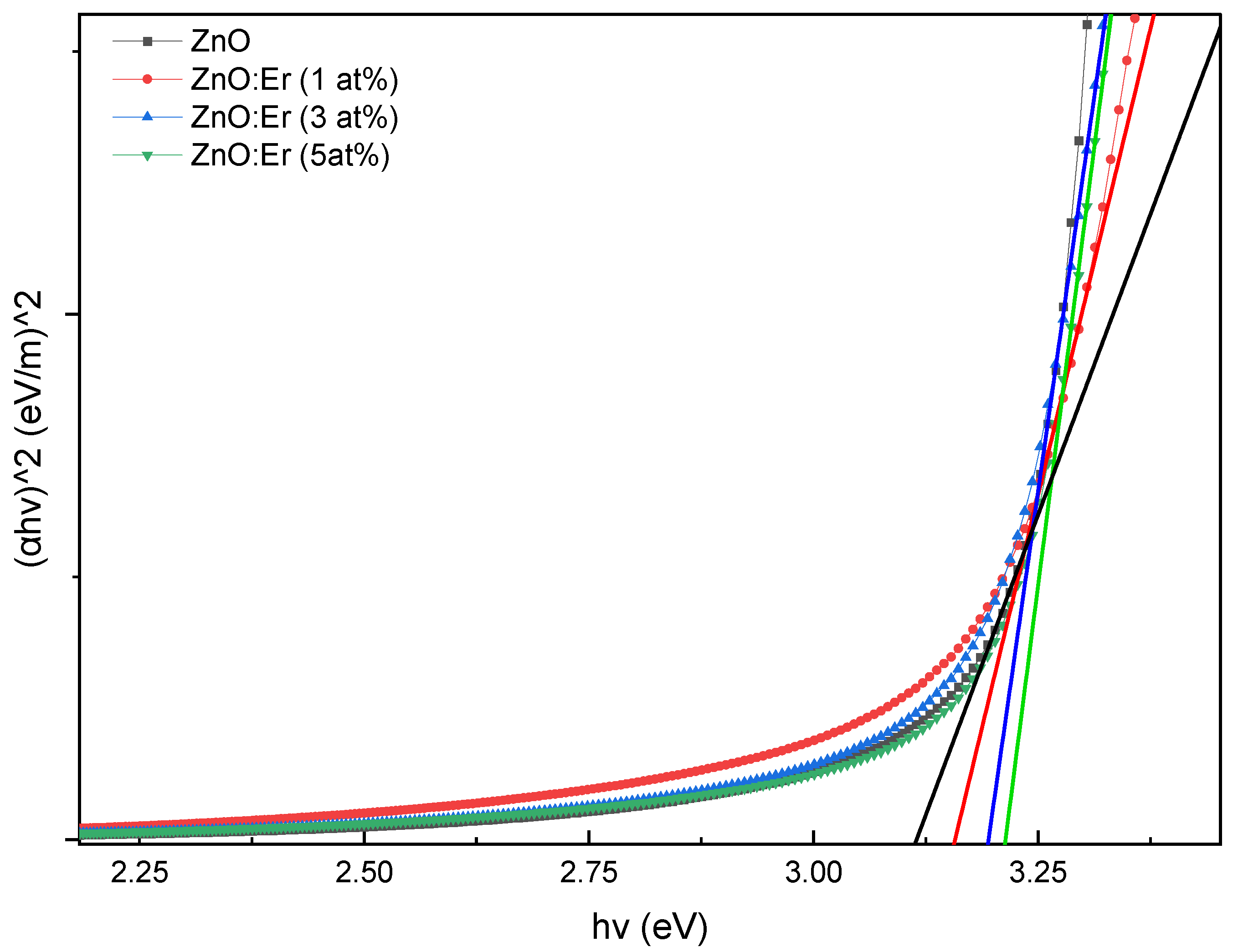
Figure 9.
Semi-logarithmic I-V characteristics of Schottky diodes fabricated on undoped and Er-doped ZnO thin films. Er doping enhances the forward/reverse current ratio and reduces reverse leakage.
Figure 9.
Semi-logarithmic I-V characteristics of Schottky diodes fabricated on undoped and Er-doped ZnO thin films. Er doping enhances the forward/reverse current ratio and reduces reverse leakage.
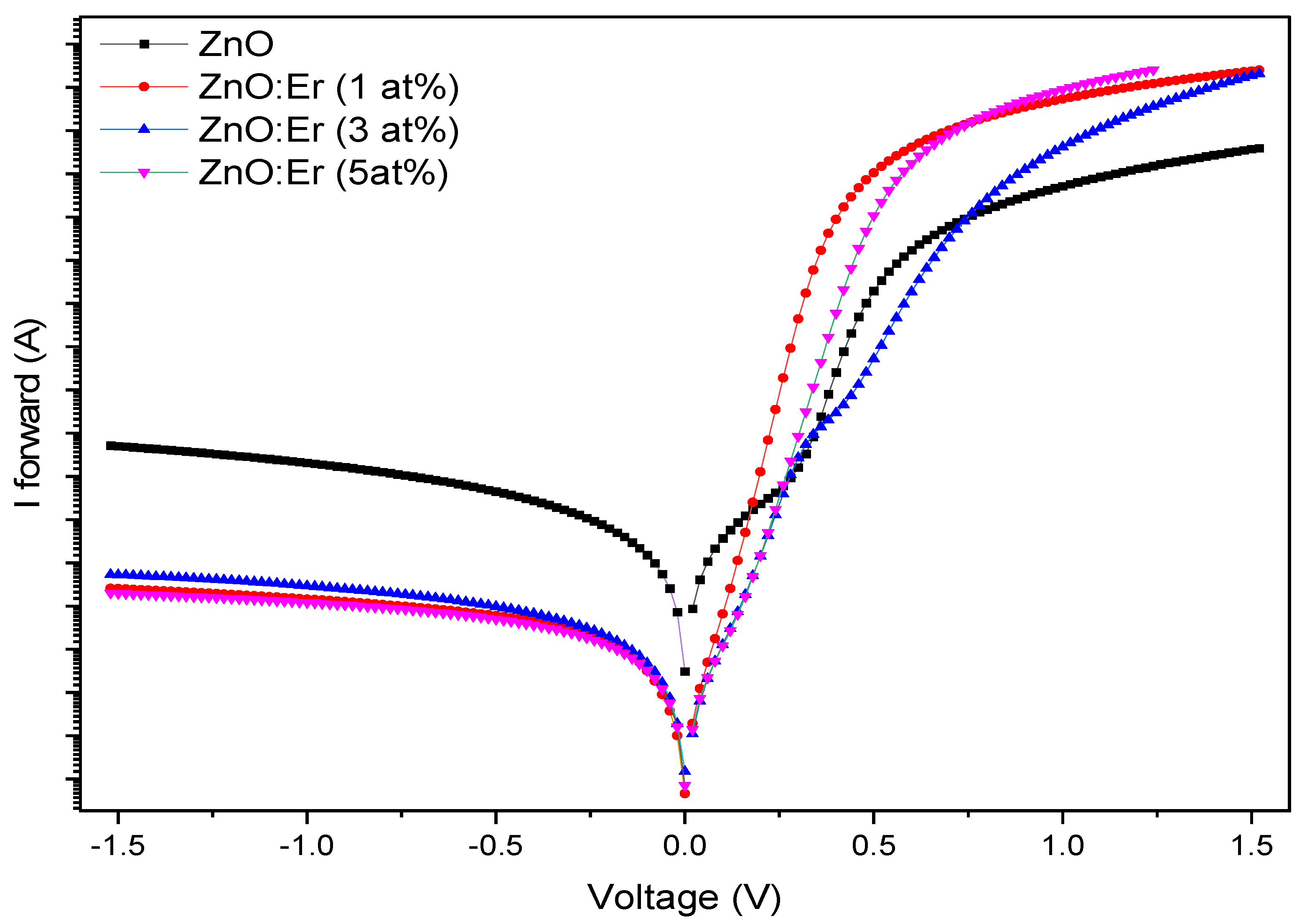
Figure 10.
Forward ln(I)-V plots for Er-doped ZnO Schottky diodes. Linear fitting in the thermionic emission region allows extraction of Schottky barrier height and ideality factor.
Figure 10.
Forward ln(I)-V plots for Er-doped ZnO Schottky diodes. Linear fitting in the thermionic emission region allows extraction of Schottky barrier height and ideality factor.
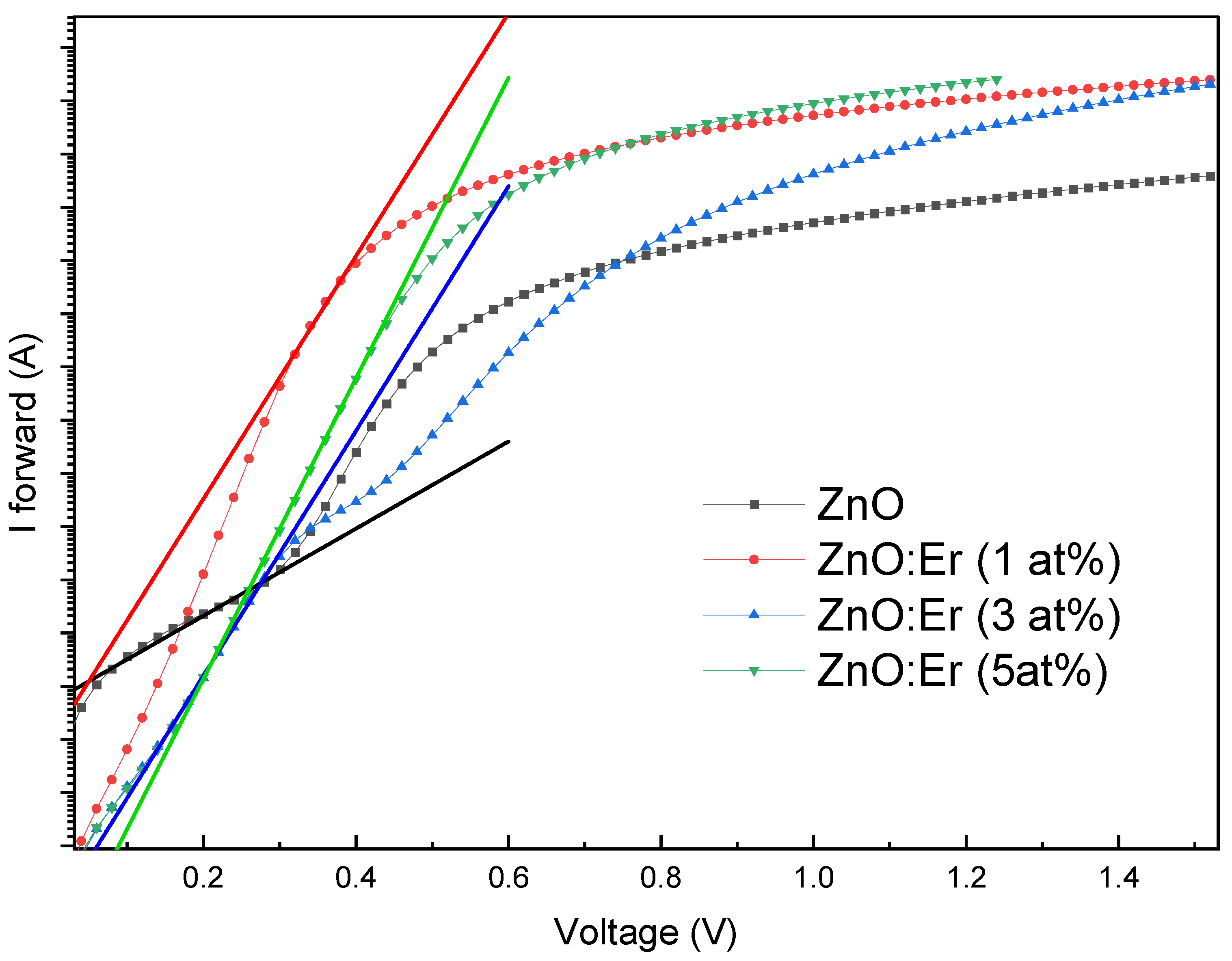
Figure 11.
Semi-log I-V curves for Schottky diodes on (Er, Yb)-co-doped ZnO thin films. Co-doping improves rectification and reduces reverse leakage current compared to undoped and Er-only doped films.
Figure 11.
Semi-log I-V curves for Schottky diodes on (Er, Yb)-co-doped ZnO thin films. Co-doping improves rectification and reduces reverse leakage current compared to undoped and Er-only doped films.
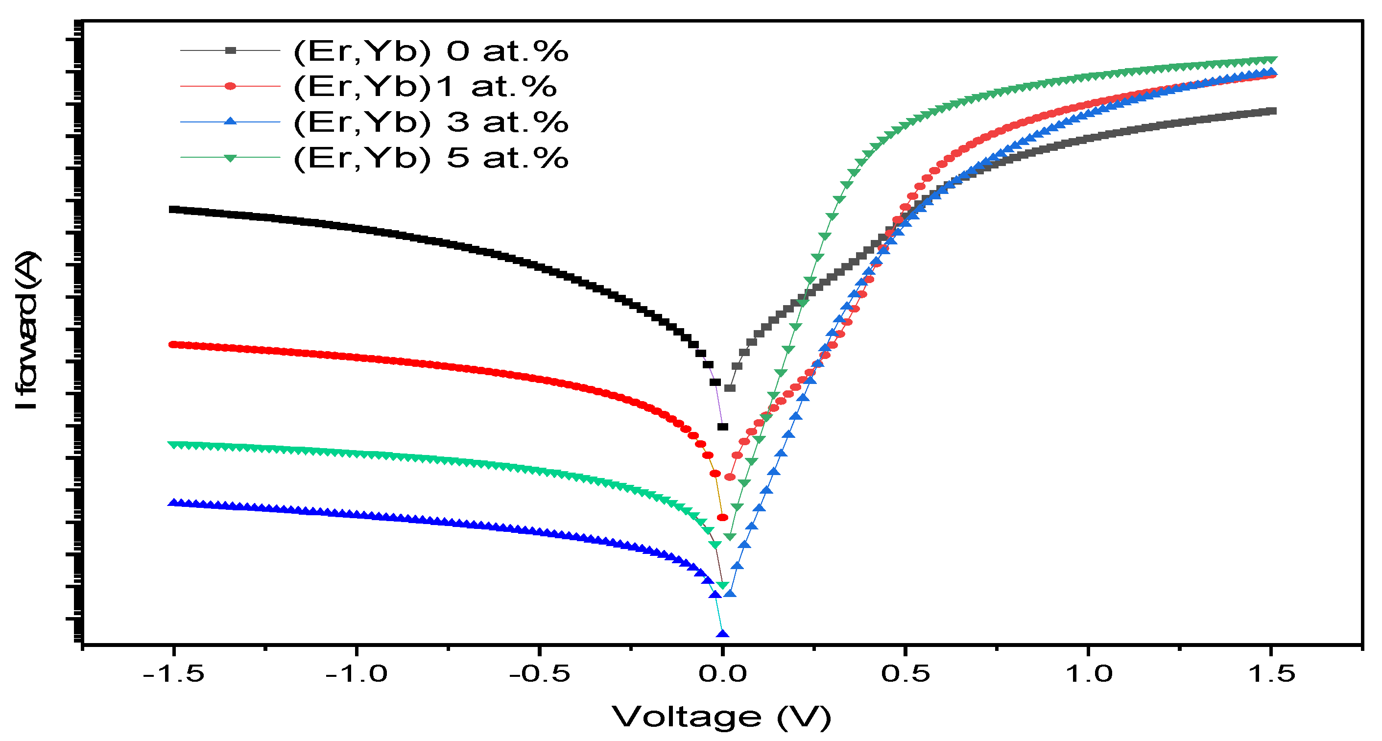
Figure 12.
Forward ln(I)-V plots for Er:Yb co-doped ZnO Schottky diodes. The extracted Schottky barrier heights and ideality factors confirm superior electrical performance due to co-doping.
Figure 12.
Forward ln(I)-V plots for Er:Yb co-doped ZnO Schottky diodes. The extracted Schottky barrier heights and ideality factors confirm superior electrical performance due to co-doping.
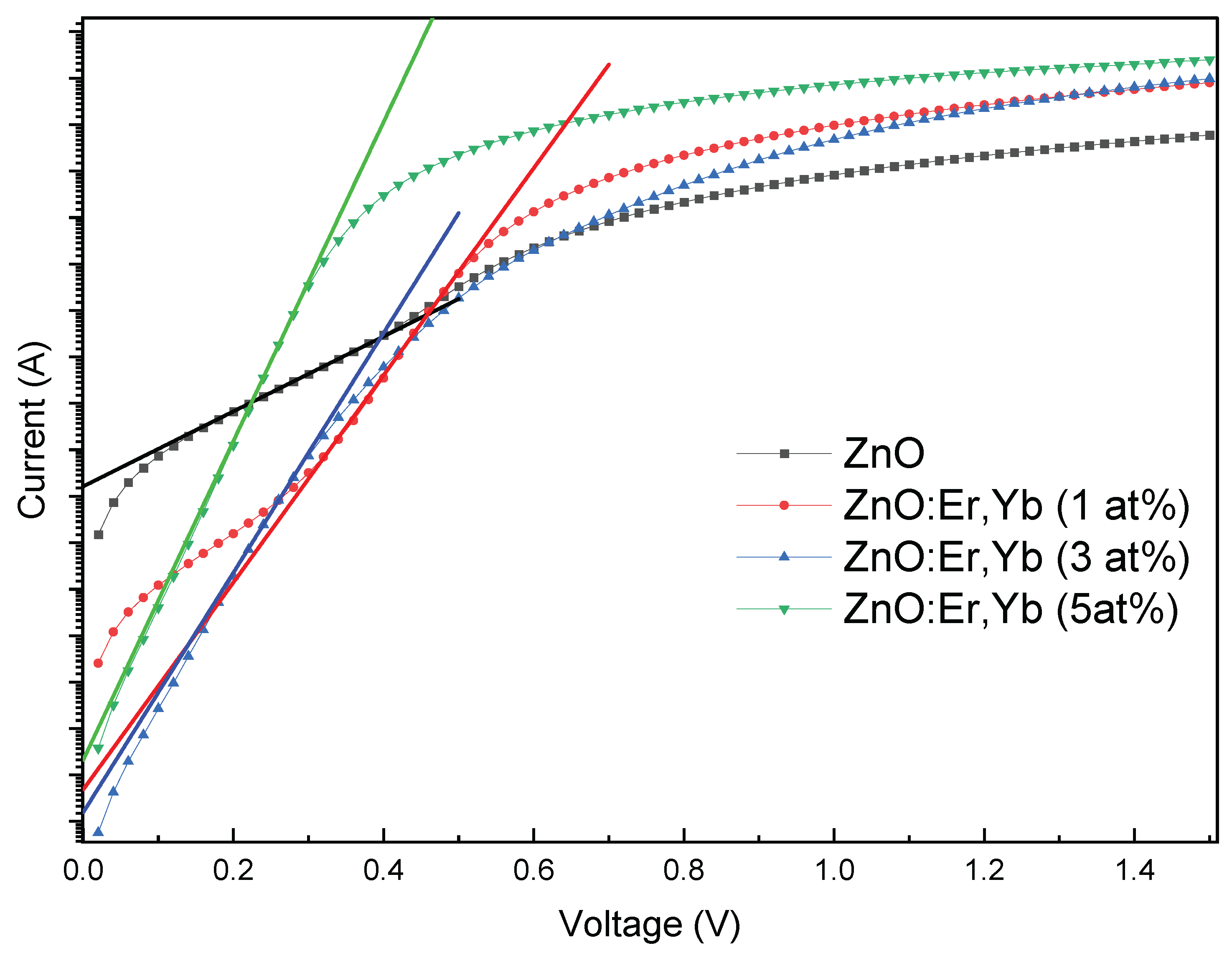

Table 2.
Structural parameters derived from XRD data.
| Sample | Doping (at.%) | 2θ (°) | FWHM (°) | TC(002) | D (nm) | δ (1012 cm−2) | ε (10−3) | a (Å) | c (Å) |
| ZnO:Er | 0 | 34.47 | 0.368 | 1.226 | 22.6 | 0.20 | 5.18 | 3.243 | 5.200 |
| 1 | 34.31 | 1.487 | 1.164 | 5.6 | 3.20 | 21.0 | 3.234 | 5.223 | |
| 3 | 34.37 | 1.236 | 1.294 | 6.7 | 2.21 | 17.4 | 3.296 | 5.214 | |
| 5 | 34.34 | 1.461 | 1.164 | 5.7 | 3.09 | 20.6 | 3.245 | 5.219 | |
| ZnO:(Er-Yb) | 0 | 35.24 | 0.480 | 1.121 | 17.4 | 0.33 | 6.59 | 3.167 | 5.089 |
| 1 | 35.21 | 0.897 | 1.146 | 9.3 | 1.16 | 12.3 | 3.165 | 5.094 | |
| 3 | 35.12 | 1.616 | 1.145 | 5.2 | 3.76 | 22.3 | 3.161 | 5.106 | |
| 5 | 34.97 | 1.668 | 1.147 | 5.0 | 4.01 | 23.1 | 3.155 | 5.128 |
Table 3.
Optical properties of Er and Er/Yb doped ZnO thin films.
| Sample | Doping (at.%) | Avg. Trans (%) | Absorp. Edge (nm) | Bandgap (eV) |
| ZnO:Er | 0 | 67.80 | 410 | 3.023 |
| 1 | 67.74 | 403 | 3.040 | |
| 3 | 64.28 | 401 | 3.059 | |
| 5 | 70.99 | 393 | 3.125 | |
| ZnO:(Er, Yb) | 0 | 66.99 | 403 | 3.113 |
| 1 | 55.51 | 383 | 3.156 | |
| 3 | 63.82 | 386 | 3.195 | |
| 5 | 64.25 | 390 | 3.214 |
Table 4.
Schottky diode parameters for Er-doped ZnO thin films.
| Sample | Doping (at.%) | Ideality Fac. (n) | Saturation Current (A) | B. Height (eV) | Resistance Rs (Ω) | L. Current @ -1.0 V | Rect. Ratio @ ±1.0 V |
| ZnO:Er | 0 | 4.77 | 8.34×10⁻⁸ | 0.655 | 512 | 6.02×10⁻⁵ | 1.4×101 |
| 1 | 1.70 | 3.98×10⁻⁸ | 0.674 | 108 | 1.12×10⁻⁶ | 2.1×10³ | |
| 3 | 1.68 | 1.38×10⁻⁹ | 0.761 | 105 | 8.45×10⁻⁹ | 2.3×10⁵ | |
| 5 | 1.38 | 4.60×10⁻¹⁰ | 0.789 | 66 | 5.92×10⁻⁸ | 1.1×10⁵ |
Table 5.
Schottky diode parameters for Er/Yb co-doped ZnO thin films.
| Sample | Doping (at.%) | Ideality Factor (n) | Barrier Height ΦB (eV) | Series Resistance Rs (Ω) | Leakage Current @ -1.0 V (A) | Rectification Ratio @ ±1.0 V |
| ZnO:Er:Yb | 0 | 4.71 | 0.595 | 386 | 5.23×10⁻⁵ | 1.6×101 |
| 1 | 1.73 | 0.758 | 225 | 9.36×10⁻⁷ | 2.6×10³ | |
| 3 | 1.50 | 0.771 | 183 | 6.94×10⁻⁹ | 2.6×10⁵ | |
| 5 | 1.13 | 0.743 | 113 | 4.81×10⁻⁸ | 1.2×10⁵ |
Disclaimer/Publisher’s Note: The statements, opinions and data contained in all publications are solely those of the individual author(s) and contributor(s) and not of MDPI and/or the editor(s). MDPI and/or the editor(s) disclaim responsibility for any injury to people or property resulting from any ideas, methods, instructions or products referred to in the content. |
© 2026 by the authors. Licensee MDPI, Basel, Switzerland. This article is an open access article distributed under the terms and conditions of the Creative Commons Attribution (CC BY) license (http://creativecommons.org/licenses/by/4.0/).
Copyright: This open access article is published under a Creative Commons CC BY 4.0 license, which permit the free download, distribution, and reuse, provided that the author and preprint are cited in any reuse.


