Submitted:
10 February 2026
Posted:
11 February 2026
You are already at the latest version
Abstract
Bismuth ferrite (BiFeO3) is a promising material for developing the next generation of multifunctional electronic devices. However, the production of high-quality BiFeO3 thin films is compromised by the tendency for structural and electronic defects to form during synthesis, which degrades their functional properties. In this work, BiFeO3 thin films were prepared by chemical solution deposition to determine optimal conditions for minimizing oxygen vacancies and to evaluate the impact of these point defects on their physical properties. The films were pyrolyzed at 300 °C for 60 min and 360 °C for 10 min, and crystallized in air and in an O2 atmosphere, at 600 °C and 640 °C for 40 min. High oxygen vacancies were observed in films prepared at low pyrolysis temperatures and crystallized in air, whereas oxygen vacancies were minimized in the film pyrolyzed and crystallized at high temperatures in an O2 atmosphere. The oxygen vacancies markedly affected the films’ physical properties, leading to increased dielectric loss, dielectric dispersion, dc conductivity, and leakage current, with consequent degradation of photovoltaic and magnetic performance. These findings highlight the critical importance of controlling synthesis parameters to suppress oxygen vacancy formation and achieve high-quality BiFeO3 thin films.
Keywords:
bismuth ferrite
; thin films
; oxygen vacancies
; point defects
1. Introduction
Bismuth ferrite (BiFeO3) is a prototypical multiferroic material characterized by a coexistence of the antiferromagnetic (TN ~ 643 K) and ferroelectric (TC = 1103 K) phases at room temperature [1,2]. Due to its large spontaneous polarization and the presence of magnetoelectric coupling at room temperature, the BiFeO3 has attracted considerable attention as a promising material with potential to develop the next generation of multifunctional electronic devices [3,4]. Controlling magnetization with electric fields and vice versa has been a frequent motivation for research into this multiferroic, with its potential for energy-efficient, high-density, and fast information storage, as well as for new concepts in sensors and logic devices. Furthermore, exploring the synthesis of BiFeO3 thin films and their physical properties is highly relevant, as nanoscale engineering is essential for integrating high-tech microelectronics and nanoelectronics. However, despite the large number of scientific articles published in recent years on BiFeO3 thin films, their effective practical technological application is not yet a reality due to several critical problems that remain unsolved.
The technological application of materials requires producing high-quality materials with rigorous control of their mechanical, physical, and chemical properties, necessary for effective use. However, the practical realization of high-quality BiFeO3 thin films is strongly hindered by the tendency to form structural and electronic defects during growth, which degrade their functional properties by increasing leakage currents [5], leading to phase instability, and reduced ferroelectric performance. Most physical property degradation is often associated with point or complex defects related to stoichiometry fluctuations [6,7], whose mechanisms include valence fluctuations of the Fe ions [8], the formation of oxygen vacancies [9], and inhomogeneities associated with the Bi volatilization during synthesis [10]. Bismuth, iron, and oxygen vacancies are the primary defects in the BiFeO3, with Bi and Fe assuming cation vacancies for charge states -3, -2, -1, 0, while oxygen vacancies appear fully ionized (), partially ionized () or neutral (). In addition, free holes and free electrons can be produced by ionized defects [11]. Bi vacancies introduce three holes in the system, while the ionization of oxygen vacancies justifies the presence of free electrons. Theoretical studies demonstrate that Bi and Fe vacancies are dominant defects in oxidizing conditions. In contrast, Bi and O vacancies are dominant under reducing conditions, leading to p-type or n-type conductivity, respectively [12]. The presence of oxygen vacancies leads to the formation of Fe2+ ions, such that both can contribute to the high leakage current. For these reasons, manipulating oxygen vacancies by Fe site substitution [13] or by doping the Bi site [14,15] have been used as alternatives that lead to practical leakage current reduction and improved photovoltaic response in BiFeO3 thin films [16]. Due to these complex defects, it is not surprising that different physical properties are often reported in the literature for the BiFeO3.
The quality of BiFeO3 thin films prepared by Chemical Solution Deposition (CSD) method via spin coating is strongly governed by the nucleation and crystallization mechanisms that occur during thermal processing [17,18]. Defect formation, phase instability, and electrical leakage are not merely consequences of processing conditions but are intrinsically linked to the kinetics and thermodynamics of perovskite phase nucleation [19] and to subsequent grain growth related to the synthesis method. Focusing attention on chemically deposited methods, nucleation and crystallization processes are closely coupled to defect chemistry, particularly oxygen vacancy formation [18,20]. Nucleation of the perovskite phase typically occurs after solvent evaporation and organic decomposition during a temperature-annealing step, often called pyrolysis, although the heat treatment occurs in the presence of oxygen [21,22]. From a thermodynamic perspective, the formation of the perovskite phase competes with secondary phases that often possess lower nucleation barriers, particularly under Bi-deficient or kinetically limited conditions. Also, bismuth's high volatility increases the critical nucleation energy of the BiFeO3 phase, favoring the formation of iron-rich parasitic phases. Introducing excess bismuth into the precursor solution is a strategy that effectively stabilizes the chemical potential of Bi and lowers the nucleation barrier for the perovskite phase [23]. Regarding crystallization kinetics, high annealing temperatures enhance grain growth but exacerbate bismuth volatilization and oxygen vacancy formation, while insufficient oxygen incorporation during crystallization leads to charge imbalance and mixed Fe2+/Fe3+ states, increasing electronic conductivity. As an alternative, annealing in oxygen-rich atmospheres and post-deposition oxygen treatments are often used to stabilize the Fe3+ state during grain growth, thereby reducing oxygen vacancy concentration. In summary, understanding the origin of these defects, their consequent effects on structural, dielectric, and electrical properties, and their effective control are fundamental challenges for promoting the transition from academic studies to the announced practical technological applications.
This work investigates the effects of processing on the control of oxygen vacancies in BiFeO3 thin films prepared by the CSD method and the consequent impact on their structural, dielectric, electrical, optical, photovoltaic, and magnetic properties. For this purpose, we produced three BiFeO3 thin films under different preparation conditions to infer how oxygen vacancies are connected with their crystallization kinetics and physical properties. Two films were prepared in an open-atmosphere electric furnace under the same pyrolysis and crystallization conditions. Nucleation at low-temperature pyrolysis induces oxygen vacancies in both films, but one of them was subjected to a long period of subsequent post-annealing in an O2 atmosphere to correct the imbalance. A third film was prepared under an O2 atmosphere at higher pyrolysis and crystallization temperatures. The main objective of the study is to make clear that, once oxygen vacancies are established during synthesis, there are practically no alternatives to correct the imbalance through subsequent actions, reinforcing the importance of controlling point defects during the nucleation and crystallization steps.
2. Materials and Methods
The BiFeO3 thin films studied in the present work were prepared from an acetic acid chemical solution route using Bi(NO3)3.5H2O (Sigma-Aldrich, 99.9%) and Fe(NO3)3.9H2O (Sigma-Aldrich, 99.9%) as starting reagents. Dissolving the appropriate amount of reagent into a solution containing 1 mL of 2-methoxyethanol (Sigma-Aldrich, 99.9%) and 5 mL of glacial acetic acid (Sigma-Aldrich, 99.9 %) at 50 °C under stirring for 10 min yielded a chemical solution. After complete homogenization, the solution temperature was raised to 80 °C, under stirring for 30 min, and then the heating was switched off. Finally, 3 mL of glacial acetic acid was added to the room temperature to obtain a final 0.16 M solution.
For film preparation, the chemical solution was initially deposited onto Pt/TiO2/SiO2/Si(100) substrates by spin coating at 5000 rpm for 30 seconds, followed by thermal annealing in an electric furnace to remove water and organics. New layers were sequentially deposited on the previously annealed films following the same protocol to increase the film thickness. After eight deposited layers, the films were crystallized in an electric furnace under an open atmosphere (air) or under an O2 atmosphere at 18.5 psi. The final films had an average thickness of ~ 400 nm. Table 1 summarizes the conditions used for the preparation of the studied BiFeO3 thin films.
Energy-dispersive X-ray spectroscopy (EDS) attached to a scanning electron microscope (Carl Zeiss EVO LS15) was used to analyze the elemental composition of the BiFeO3 thin films. The crystalline structure of the films was characterized by X-ray diffraction (XRD) using a Rigaku Ultima IV diffractometer with CuKα radiation (λ = 1.5406 Å) at room temperature, under 40 kV and 40 mA at the 20° ≤ 2θ ≤ 60° range. Raman measurements were performed using a confocal Raman BX51 Voyage TM with 785 nm laser excitation and spectral resolution of 3 cm−1.
X-ray photoelectron spectroscopy (XPS) was used to study the chemical properties and valence states of the BFO films. The XPS spectra were acquired in an Ultra High Vacuum (UHV) system with a base pressure of 2.10–10 mbar. The system is equipped with a hemispherical electron energy analyzer (SPECS Phoibos 150), a delay-line detector, and a monochromatic AlKα (1486.74 eV) X-ray source. High-resolution spectra were recorded at a normal emission take-off angle and with a pass energy of 35 eV, which provides an overall instrumental peak broadening of 0.65 eV.
For the electrical measurements, gold electrodes of 300 μm in diameter were sputtered onto the films using a shadow mask to form metal/ferroelectric/metal capacitors. An Agilent 4284A LCR meter was used to measure the complex dielectric permittivity (), impedance (), the electric modulus , and the ac electric conductivity () at different frequencies (102 - 106 Hz) and temperatures (300-500 K). For the analysis of impedance spectroscopy data, an equivalent circuit composed of a series combination of RC and RC-CPE components was considered [24,25], representing the effects of grains and grain boundaries, respectively. The introduced constant phase element (CPE) indicates a departure from the ideal Debye model. From the model, the following equations for the real and imaginary parts of impedance and electric modulus were used to fit the experimental data as a function of the angular frequency ():
where ( is the sample thickness and the electrode area), is the grain resistance, the grain capacitance, the grain boundary resistance, and the grain boundary capacitance.
The leakage current-voltage () and photovoltaic characteristics of BiFeO3 films were characterized using a Keithley 6517B electrometer. The photovoltaic responses were obtained by illuminating the films between the electrodes with a monochromatic green laser λ = 532 nm ( = 2.33 eV). Magnetic measurements were performed using a Quantum Design PPMS-VSM magnetometer at an H sweep rate of 30 Oe/s. The magnetization as a function of temperature was measured under zero-field cooling (ZFC) and field cooling (FC) regimes in the temperature range 5 - 390 K, and the magnetization hysteresis loops were measured at 5 K and 300 K with an applied magnetic field within ± 30 kOe.
3. Results and Discussion
The prepared BiFeO3 films for the present study had homogeneous, smooth, and crack-free surfaces. Atomic elemental analysis by EDS quantifies stoichiometry across eight different surface areas and confirms the nominal composition of the synthesized BiFeO3 films within experimental accuracy. Figure 1 shows the EDS spectra and corresponding scanning electron micrograph images used for statistical analysis and quantification. The atomic percentages of the elements from the statistical analysis and the corresponding Bi/Fe, O/Bi, and O/Fe molar ratios were summarized in Table 2.
3.1. Structural Analysis
The long-range crystalline structure of the studied films was characterized by X-ray diffraction, and Raman microscopy complements the short-range order structural analysis. Figure 2(a) shows the observed and calculated XRD patterns of the studied BiFeO3 thin films at room temperature, and Figure 2(b) shows Raman spectra recorded from the same samples. In Figure 2(a), no preferred orientations were observed for all XRD patterns, and the indexed (hkl) peaks refer to the rhombohedral structure of the BiFeO3 with an space group. The peaks Pt(111) and Pt(200) refer to the cubic phase (a = 3.892 Å) of the platinum substrate with an space group. A single-phase BiFeO3 is observed in Figure 2(a) for the BFO1 film, pyrolyzed at 300 °C and crystallized in air at 600 °C without post-annealing. On the other hand, traces of the secondary Bi25FeO39 and Bi2Fe4O9 phases were observed in coexistence with the BiFeO3 phase for the BFO2 and BFO3 films, pyrolyzed at 300 °C and crystallized in air at 600 °C with an additional post annealing in oxygen atmosphere, and pyrolyzed at 360 °C and crystallized in oxygen atmosphere at 640 °C without post annealing, respectively. The calculated profiles were obtained by Rietveld refinements of the XRD patterns using the rhombohedral phase with space group of the BiFeO3. The parameters obtained from refinements are summarized in Table 3. The obtained lattice parameters and the volume cell are very similar for all samples and are in good agreement with those reported for BiFeO3 single crystals [26]. From a structural perspective, no differences were observed in the studied films due to variations in processing under different annealing atmospheres. On the other hand, the different crystallization temperatures strongly influence the intensity of the XRD peaks. The intensity of the XRD peaks is associated with the number of atoms in the crystal contributing to the diffraction, such that higher peak intensities indicate a higher degree of crystallinity. The more intense X-ray diffraction peaks indicate higher crystallinity for the BFO3 film, while the lower peak intensities indicate moderate crystallinity for BFO2 and lower crystallinity for the BFO1 sample. As BFO2 and BFO1 films were prepared at the same crystallization temperature (600 °C) under different atmospheres, the very similar XRD peak intensities indicate that the annealing atmosphere has no pronounced effects on the crystallinity. In contrast, the increase in crystallization temperature (640 °C) of the BFO3 film leads to higher crystallinity, indicating that temperature is more effective in improving the film crystallinity. In addition, the slope of the plot drawn between versus from the Williamson-Hall approach in Figure 2(c) gives the values of microstrain, while the y-intercept gives the values of crystallite size. For the studied BFO1, BFO2, and BFO3 films, the obtained crystallite sizes were 43, 48, and 45 nm, while the microstrains were 1.2 x 10⁻³, 1.3 x 10⁻³ and 1.1 x 10⁻³, respectively. Despite the expected link between synthesis and processing conditions, the crystallite sizes and microstrains present essentially the same values for the different films.
Figure 2(b) shows the Raman spectra of the three studied BiFeO3 films, recorded at room temperature in the range of 100-600 cm-1. According to the group theory, BiFeO3 with rhombohedral structure exhibits 13 (4A1 + 9E) Raman-active modes, which were fitted in Figure 2(b) using Lorentzian curves for each mode. The assignment for the Raman modes of the studied BiFeO3 films is summarized in Table 4 and compared with results from the literature for single crystals [27] and epitaxial BiFeO3 thin films [28]. The peaks at 141, 174, 220, and 430 cm-1 are A1-symmetry longitudinal-optical A1(LO) phonons, while the peaks at 260, 281, 349, 371, 469, 480, and 527 cm-1 are all related to the transverse-optical E(TO) modes, considering as a reference the Raman spectrum of the BFO3 film. Similarly to the observed in the XRD patterns in Figure 2(a), the higher Raman intensity peaks in Figure 2(b) of the BFO3 film, which was crystallized at a higher temperature (640 °C), compared to the BFO1 and BFO2 films, confirm its higher crystallinity. On the other hand, the increase or decrease in Raman shift provides a powerful tool for probing property changes directly affected by the synthesis conditions, since Raman frequency shift is susceptible to internal and external factors associated with structural and physical properties, such as crystallite size, crystallinity, phase composition, oxygen vacancies, defects, strain, and compressive/tensile stresses. The Raman shift of the A1(LO) modes in the BFO2 film shifts to lower frequencies or longer wavelengths (red shift), in comparison to the BFO1 film modes around 144 cm-1 and 177 cm-1, as shown in Figure 2(d). Despite the red shift often being attributed to improved crystallinity in the literature, this does not appear to be the case, as BFO1 and BFO2 exhibit similar crystallinity, whereas BFO3 shows higher crystallinity. The redshift in the BFO2 film indicates a direct effect of the synthesis conditions, possibly associated not only with oxygen vacancies, as will be discussed below, but also with other defects that could not be explicitly identified.
3.2. X-Ray Photoelectron Spectroscopy Analysis
XPS measurements were conducted to determine the oxidation states, chemical shifts, and oxygen vacancies in the studied BiFeO3 films. Figure 3 shows the XPS spectra of the (a) Bi 4f, (b) Fe 2p, and (c) O 1s core levels for the studied BiFeO3 thin films. Figure 3(a) shows that the Bi 4f core levels of all samples are also similar, such that Bi 4f7/2 and Bi 4f5/2 were centered at BEs of 158.9 eV and 164.2 eV, with a spin-orbit splitting of 5.3 eV. These results were ascribed to Bi3+ and agreed with reports in the literature for BiFeO3 thin films [29]. In Figure 3(b), the Fe 2p regions were fitted by using a Shirley background and Lorentzian functions. For all samples, the Fe 2p core levels were quite similar. They presented two main peaks ascribed to Fe 2p3/2 and Fe 2p1/2 with a spin-orbit splitting of 13.6 eV. Furthermore, the results in the present work reveal the coexistence of Fe2+ and Fe3+ ions in the studied BiFeO3 films. Moreover, a satellite peak related to Fe2+ and Fe3+ ions clearly appeared in the spectra at a binding energy (BE) of about 718.6 eV [30], as indicated in Figure 3(b). This satellite peak is characteristic of oxidized Fe atoms. On the other hand, the main peaks could be fitted by two components that correspond to Fe3+ and Fe2+ [31,32] centered at BEs of about 711.5 eV and 709.9 eV, respectively. While Fe3+ was ascribed to the Fe atoms in the pristine BiFeO3 samples, Fe2+ derives from the surface defects, i.e., oxygen vacancies [29].
Despite reports in the literature stating that the satellite peak for Fe 2p3/2 at a difference of 8 eV indicates only the Fe3+ presence, the asymmetries observed in Figure 3(b) for both Fe 2p3/2 and 2p1/2 peaks clearly suggest a coexistence of Fe2+ and Fe3+ in the present case. In this case, the satellite peak will also be a combination of Fe2+ and Fe3+ effects. The obtained Fe3+/Fe2+ = 2.1 ratios between the oxidation states of Fe were essentially the same for all films. Therefore, Fe2+ and Fe3+ ions coexist in the studied BiFeO3 thin films, but Fe3+ ions are predominant compared to Fe2+ ions. The presence of Fe2+ ions is indicative of the existence of oxygen vacancies, since leads to [29].
The O 1s core levels exhibit three peaks labelled OI, OII, and OIII in Figure 3(c), which are attributed to the oxygen-metal bond, the dangling bond, and surface-adsorbed oxygen, respectively, as previously reported for BiFeO3 thin films [29]. The OI peak at ~ 529.6 eV remains constant across all studied BiFeO3 films. The OII peak appeared at binding energies ~ 532.3 eV in BFO1 and BFO2 films, and ~ 531.7 eV in BFO3 film, while the OIII peak appeared at ~ 534.0 eV in BFO1 and BFO2 films and is not present in BFO3 film, pyrolyzed at 360 °C and crystallized in O2 atmosphere at 640 °C. The OII peaks are higher than OI peaks for both BFO1 and BFO2 films, while the OI peak is higher than OII peak in the BFO3 film, indicating a strong influence of the processing on the oxygen vacancies and adsorbed oxygen in the final films. In addition, the asymmetry observed in Figure 3(c) at OII peak in XPS spectra of BFO1 film, pyrolyzed at 300 °C and crystallized in open atmosphere (in air) at 600 °C, suggests the coexistence of oxygen vacancies with different oxidation states (, ). The OIII is ascribed to oxygen vacancies with higher oxidation states () as plausible defects in the BiFeO3 system [11]. So, the XPS spectra of BFO films were fitted using three Lorentzian functions to simulate the presence of and oxygen vacancies, in addition to the lattice oxygen. Previous works indicated that OII is related mainly with hydroxyl groups occupying the oxygen defects in BiFeO3 films [29,31], but also with oxygen contamination, including oxidized organic groups and adsorbed H2O [33]. In our case, although post-annealing in an O2 atmosphere potentially reduces the oxygen vacancies compared to the film crystallized at the same temperature (600 °C) in an open atmosphere, the pyrolysis at low temperature (300 °C) probably plays a more prominent role in introducing defects associated with incomplete organic removal during the layer-by-layer film deposition.
The oxygen vacancy content can be estimated from the relative peak’s intensity ratio () relation , such that , and are the relative peak intensities of the oxygen-metal bond, dangling bond, and adsorbed oxygen, respectively [34]. Thus, a lower value indicates a higher concentration of oxygen vacancies. The calculated values of the BFO1, BFO2, and BFO3 films, from fits in Figure 3(c), were 0.30, 0.55, and 2.26, respectively, indicating that the concentration of oxygen vacancies is higher in the BFO1 film and lower in the BFO3 film, while the BFO2 film shows an intermediate concentration of oxygen vacancies. The values indicate that the total oxygen vacancy () is smaller in the film post-annealed in an O2 atmosphere (BFO2) than in the film crystallized in an open atmosphere (BFO1), both of which were crystallized at the same temperature (600 °C). These results indicate that the decrease in oxygen vacancies in BFO2, compared to the BFO1 film, lowers the OIII oxygen density, suggesting that post-annealing in an oxygen atmosphere reduces surface-adsorbed oxygen. Also, the oxygen vacancies are not neutral in these films but fully ionized () or partially ionized (). Furthermore, increasing the pyrolysis temperature to 360 °C for 10 min and crystallizing at 640 °C for 40 min under an O2 atmosphere significantly reduces oxygen vacancies in the BFO3 film, indicating the importance of establishing ideal conditions for defect control during synthesis.
3.3. Dielectric Properties and Conductivity
Defects such as oxygen vacancies, valence changes of Fe3+ to Fe2+ ions, and other point defects significantly modify the dielectric and electrical properties of BiFeO3 thin films. The frequency dependence of the real () and imaginary () parts of the dielectric permittivity at room temperature of the studied BiFeO3 thin films (BFO1, BFO2, and BFO3) is shown in Figure 4(a) and 3(b). All films show normal dielectric dispersion in both figures, i.e., and decreases with increasing frequency and gradually stabilize above ~ 10⁴ Hz. In Figure 4(a), a lower permittivity ( = 37 at 100 kHz) almost frequency independent was observed for the BFO3 film, pyrolyzed at 360 °C and crystallized at 640 °C in an O2 atmosphere, while higher permittivities ( = 153 and 165 at 100 kHz) increasing at low frequencies (~ 100 Hz) are observed for the BFO1 and BFO2 films, both pyrolyzed at 300 °C and crystallized at 600 °C, in an open atmosphere (in air) and post-annealed in an O2 atmosphere, respectively. Although the obtained permittivity values agree with different reports in the literature for BiFeO3 thin films prepared from chemical or physical routes, it is important to note that the lower permittivity of the BFO3 film indicates that pyrolysis and crystallization at higher temperature and in an O2 atmosphere were effective in minimizing point defects, compared to BFO1 and BFO2 films with higher defects. In addition, post-annealing in an O2 atmosphere for the BFO2 film was favorable for the formation of secondary phases and introduced additional defects, allowing mobile charge carriers to accumulate at interfaces or grain boundaries, resulting in significant space charge polarization known as the Maxwell-Wagner-Sillars interfacial polarization [35]. Thus, the higher apparent dielectric permittivity of these last films indicates a space charge polarization effect, which is more pronounced at lower frequencies, as clearly observed in the BFO2 film.
In Figure 4(b), BFO3 exhibits the highest dielectric loss (~57) at low frequencies, indicating possibly higher leakage currents. At frequencies above ~ 10⁴ Hz, BFO2 exhibits a higher (~ 10), while BFO1 and BFO3 show very similar behavior and much lower losses (~ 2), with BFO1 having the lowest value, approaching zero at high frequencies (~ 0.7 at 1 MHz). The decrease in both and with increasing frequency, it can be understood by considering carriers in the dielectric material hopping from highly conductive grains to grain boundaries with lower conductivity, from highly conductive grains compared to grain boundaries ( > ), in an analogy with the heterogeneous model of the polycrystalline structure given by Koops [36]. This means that increasing the frequency of the applied field decreases the probability that carriers reach the grain boundary. Consequently, the polarization produced by the migratory species decreases as it accumulates at the grain boundaries. Thus, the observed behaviors for and in Figure 4(a) and Figure 4(b) have become comprehensive in the view of this model. As the decrease of reflects the reduced conductive contribution in the sample, lower values of indicate thin films with lower conductivities.
Figure 4(c) shows the frequency-dependent ac conductivity () of BiFeO3 thin films (BFO1, BFO2, and BFO3) in the range 10²-10⁶ Hz, plotted on a log-log scale. The ac conductivity can be described by the power-law relation , as proposed by Jonscher [37]. Often used for different materials, in this equation is the frequency independent conductivity, represents the dielectric dispersion, while the exponent and the coefficient are parameters dependent on temperature and material. The red lines in Figure 4(c) are theoretical fits using the Jonscher model. For the BFO3 film, the frequency-independent plateau-like region observed at low frequencies ( < 1 kHz) is attributed to the conductivity, which is expected to be frequency-independent at . The plateau at room temperature and lower frequencies suggests a dc conduction behavior, indicating a single relaxation process in the BFO3 film [38]. On the other hand, no plateaus were observed in the conductivity curves of the BFO1 and BFO2 films within the studied frequency range. From the fittings in Figure 4(c), the obtained dc conductivities at room temperature were = 1.2 x 10⁻¹⁰, 3.6 x 10⁻¹⁰ and 2.7 x 10⁻⁹ S.cm-1 for the BFO1, BFO2, and BFO3 films, respectively. These results are comparable with those reported in the literature for BiFeO3 thin films obtained from rf-sputtering ( ~ 2.8 x 10⁻¹⁰ S.cm-1 [38]) and for films obtained by chemical solution method ( ~ 8.0 x 10⁻⁸ S.cm-1), whose differences indicates the influence of the synthesis route.
The temperature dependence of the real () and imaginary () dielectric permittivities of the studied BiFeO3 thin films (BFO1, BFO2, and BFO3), measured at different frequencies from 100 Hz to 1 MHz, in the temperature range 300 - 500 K, is shown in Figure 4(d) and Figure 4(e), respectively. For the BFO1 and BFO2 films, both and increases gradually with temperature for all frequencies, showing a stronger rise above ~ 400 K. For these films, the pronounced increase in near 450 - 500 K suggests space charge or interfacial polarization contributions, possibly at grain boundaries, since the temperature dependence indicates thermally activated polarization processes. The frequency dispersion in below ~ 10 kHz corroborates the presence of space-charge relaxation arising from inhomogeneous microstructures induced by defects. A similar increase in with temperature is also observed in BFO3 film, with a sharp rise above ~ 375 K, but the increase in is approximately linear in a log scale, following an Arrhenius-type loss behavior.
3.4. Impedance Spectroscopy Analysis
Impedance spectroscopy is a powerful tool for separating the contributions of grains and grain boundaries to the transport properties of materials, providing important insights into the dielectric relaxation mechanisms. Figure 5 shows the frequency dependence of the normalized imaginary parts () of impedance and () of electric modulus for studied BiFeO3 thin films (BFO1, BFO2, and BFO3) at selected temperature range. The peaks shifting to high frequencies with increasing temperature confirm a thermally activated dielectric relaxation in these BiFeO3 films, so that the hopping mechanism of charge carriers dominates. Increasing the temperature provides more thermal energy for the charge carriers, allowing them to move faster, and leading to a decrease in relaxation time and a peak shift towards higher frequencies. Only a single relaxation peak () was observed for BFO1, BFO2, and BFO3 films in Figure 5 (top), while for the electric modulus in Figure 5 (bottom), a single relaxation peak () was observed for BFO3 film in Figure 5(c), but the presence of two peaks were observed for BFO1 and BFO2 films in Figure 5(a) and (b), which can be associated with grain and grain boundary contributions. Point defects, especially oxygen vacancies, increase the number of mobile charge carriers and have a significant effect on the electric modulus () peak. Since defect-related carriers respond more readily to the alternating electric field, the Mʺ peak often shifts to higher frequencies, indicating a faster relaxation process. However, if defects are more complex and trap charge carriers, they can shift the spectrum to lower frequencies, reflecting slower relaxation. From Figure 5 (bottom), the peak of the electric modulus () at 480 K was observed at ~ 3.7 kHz, 570 Hz, and 38.4 kHz for BFO1, BFO2, and BFO3 films, respectively. It indicates that the relaxation peak shifts to lower frequencies for the BFO1 and BFO2 films, compared to the BFO3 film. The pyrolysis of BFO1 and BFO2 films at a low temperature (300 °C) differs significantly from that of the BFO3 film at a higher temperature (360 °C) in promoting the formation of oxygen vacancies due to incomplete organic removal. This partially explains the high concentration of oxygen vacancies in the BFO1 and BFO2 films, and the low concentration in the BFO3 film, as shown in Figure 3(c). Although the post-annealing in an O2 atmosphere for the BFO2 film potentially reduces the oxygen vacancies compared to the BFO1 film, crystallized in an open atmosphere at the same temperature, the process is favorable to the crystallization of traces of secondary phases, introducing additional defects that favor the trapping of charge carriers, which leads to the observed shift of the peak to lower frequencies.
Figure 6(a), (b), and (c) shows the frequency dependence of the real () and imaginary () parts of the impedance of the BFO1, BFO2, and BFO3 films, at selected temperatures, while the frequency dependence of the real () and imaginary () electric modulus are shown in Figure 6(d), (e), and (f). The lines in these figures refer to the theoretical results obtained by using Equations (1) to (4). The plots in these figures are shown on a logarithmic scale to explicitly demonstrate the good agreement between the experimental data and the theoretical fits, as the fit accuracy can be obscured when the impedance data are presented on a linear scale. The good fits of and , considering effects of grain boundary at low frequencies and grain at high frequencies, confirm the presence of a non-Debye type of relaxation in these samples.
Figure 6(g), (h), and (i) compare the frequency dependence of the normalized imaginary impedance () and imaginary electric modulus () at two particular temperatures for the studied BFO1, BFO2, and BFO3 films. These combined plots of impedance () and electric modulus () as a function of frequency are a valuable tool for inferring the conduction mechanism and distinguishing relaxation processes associated with the short-range or long-range motion of charge carriers in ferroelectric thin films [39]. An appreciable mismatch is observed at the and of the BFO1 and BFO2 films, while an almost perfect overlap is observed for the BFO3 film. Slight overlapping of the Z″ and M″ peaks confirms that the relaxation process departs from ideal Debye-type behavior and indicates the predominance of grain boundary response for the BFO3 film within the studied frequency and temperature range, corroborating what was observed in Figure 5(c).
For several solid materials, the frequency at which the and peaks occur correspond to the transitions from long-range (delocalized) to short-range (localized) relaxation. The overlapping of the and peaks indicate long-range relaxation, whereas an appreciable mismatch between these peaks is associated with the coexistence of both short and long-range relaxation [40]. In typical dielectric materials, localized relaxation dominates so that the electrical response is more effective in terms of permittivity and dielectric loss. On the other hand, long-range conductivity dominates ionic conductive materials so that the impedance and the electric modulus better reflect the response. For a physical process that exhibits a distribution of relaxation time, the imaginary parts of the impedance and the electric modulus show different relaxation times such that separated and peaks characterize short-range relaxation and overlapped peaks indicate long-range relaxation [40]. Thus, the two partially overlapping relaxation and peaks in Figure 6(i) suggests a predominance of long-range relaxation in the BFO3. In contrast, the observed mismatch between the and peaks in Figure 6(g) and (h) indicates the coexistence of both short and long-range relaxation in the BFO1 and BFO2 films, most likely associated with the coexistence of electron/hole hopping and diffusion of oxygen vacancies, most introduced due to low-temperature pyrolysis during the synthesis of these films.
The activation energies were evaluated from the Arrhenius relations for the dc conductivity , where is a pre-exponential factor, is the Boltzmann constant, and is the activation energy. From the and values obtained from theoretical fits of the impedance and the electric modulus in Figure 6, the dc conductivities () associated with the grain and grain boundary were obtained, considering the relation , where (film thickness) and (electrode area) are geometrical parameters. Thus, Figure 7 shows the reciprocal temperature dependence for both the grain and grain boundary, whose the respective activation energies were evaluated from linear fits in this figure. The inset table in Figure 7 summarizes the obtained activation energies for grains and grain boundaries. The grain and grain boundary activation energies were 0.71 eV and 0.81 eV for the BFO1 film, and 0.76 eV and 1.40 eV for the BFO2 film. Both films were pyrolyzed at 300 °C, crystallized at 600 °C in an open atmosphere (in air), and post-annealed in an O2 atmosphere, respectively. On the other hand, for the BFO3 film, pyrolyzed and crystallized at a higher temperature and in an O2 atmosphere, the activation energies for the grain and the grain boundary were the same and equal to 0.44 eV. The different activation energies indicate that distinct mechanisms are responsible for electrical conduction in the studied films, indicative of defects introduced during synthesis.
In the literature, different values of activation energies have been reported for BiFeO3 thin films. For films prepared by rf-sputtering, two distinct conduction activation energies of 0.37 eV and 0.73 eV were reported [38], attributed respectively to the first ionization of oxygen vacancies and to electron hopping for conduction at low temperatures, and to the thermal excitation of carriers from the second ionization of oxygen vacancies. For La-Ti-co-doped BiFeO3 films, the activation energies of 0.46 and 0.47 eV for the grain and grain boundary, respectively, were associated with the first ionization of oxygen vacancies [38]. Furthermore, studies on the fatigue process of polycrystalline BiFeO3 thin films revealed that defect evolution during polarization switching reduces the activation energy from 0.9 eV to 0.2 eV [41]. Independent of defect type, there is consensus that oxygen vacancies play an essential role in the mechanism responsible for dielectric relaxation and electric conduction in BiFeO3 [38]. In this scenario, the grain and grain boundary activation energies for the BFO1 (0.71 eV and 0.81 eV) and BFO2 films (0.76 and 1.40 eV) indicate a conduction mechanism associated with the second ionization of oxygen vacancies in these films. In contrast, the first ionization of oxygen vacancies governs the conduction mechanism in both grains and grain boundaries of the BFO3 film (0.44 eV), a consequence of reduced defect concentration in this sample.
3.5. Leakage Current and Photovoltaic Properties
Figure 8(a) shows typical leakage current density electric field () characteristics of the studied BiFeO3 films in the dark condition, measured at room temperature for both negative and positive biases in the electric field range of ± 50 kV/cm. In this figure, the curves show similar shapes with the positive and negative branches symmetrical for the BFO1 and BFO2 films, pyrolyzed at 300 °C, crystallized at 600 °C in an open atmosphere (in air), and post-annealed in an O2 atmosphere. In contrast, for the BFO3 film, pyrolyzed and crystallized (in O2 atmosphere) at higher temperatures, the positive and negative branches are slightly asymmetrical, such that its leakage current density (23 μA/cm2) at 50 kV/cm is one order of magnitude lower than that of the BFO1 (123 μA/cm2), and 3.6 times smaller than the leakage current density for the BFO2 (84 μA/cm2) film, which present a similar behavior compared to BFO1.
A leakage current in BiFeO3 thin films has often been attributed mainly to oxygen vacancies [16], as several studies have shown that reducing their concentration minimizes leakage current in ferroelectric thin films. As demonstrated by the values from XPS results, the BFO1 film shows the highest concentration of oxygen vacancies among the samples studied, the BFO2 film shows an intermediate concentration, and the BFO3 film shows the lowest concentration. The observed leakage current density follows the concentration of oxygen vacancies in the studied films, suggesting a correlation. However, the mechanisms of leakage current can be more intricate and may correlate with defects associated with the Bi/Fe and Fe3+/Fe2+ ratios rather than with the oxygen vacancy concentration. Deviation changes the Fe ions' valence from Fe3+ to Fe2+, leading to highly conductive samples, while equation describes the origin of bismuth vacancies and the consequent Bi2O3 formation [42]. Bi vacancies introduce three holes in the system, and the presence of Fe2+ and oxygen vacancies with different valence states justifies the presence of free electrons. In the BiFeO3 system, deep localized oxygen vacancy traps the holes, and the charge neutrality condition determines the equivalence or not between the free electrons and holes [12]. Thus, it is plausible that free electrons and holes compensate for the charge, mutually remaining in a competition between Bi and oxygen vacancies. This scenario shows that the synthesis process is fundamentally important to control defects during the preparation of BiFeO3 thin films. According to the EDS analyses, the Bi/Fe ≈ 1 for all studied films within experimental accuracy, while from XPS analyses, the Fe3+/Fe2+ ≈ 2 for all films, indicating the coexistence of Fe2+ and Fe3+ ions, with the predominance of Fe3+ ions. Although the presence of a small amount of secondary phases in films BFO2 and BFO3 should act as significant sources and mediators for various defects, the results indicate that oxygen vacancies are the main factor contributing to the leakage current in the studied films.
The analysis of conduction mechanisms offers additional insights into the conductivity. Among different mechanisms, the ohmic is given by the linear relation , where is the electrical conductivity and generally dominates in the regime of low electric fields. The SCLC mechanism is provided by the relation , where is the charge mobility, the vacuum permittivity, the low-frequency relative dielectric permittivity and the sample thickness [43]. Figure 8(b) shows versus plots of the studied BFO films for positive bias. The linear fits to the curves at electric fields below 30 kV/cm yield slopes ~ 1 for all films, as shown in Figure 8(b), confirming ohmic conduction at low electric fields and excluding the SCLC mechanism for these films within the studied electric field range.
The measured photocurrent densities (JSC) of the studied BiFeO3 films at short-circuit conditions are shown in Figure 9 under light-on and light-off illumination, alternated for 2 s and repeated 4 times. Under illumination, all studied BFO films show a clear and distinct photovoltaic response. The most significant photocurrent density of the BFO3 film (~ 2.97 μA/cm-2) is about 6.9 times higher than the lowest value observed for the BFO1 film (~ 0.43 μA/cm-2), and about 1.7 times higher than the photocurrent density of the BFO2 film (~ 1.72 μA/cm-2). The highest photocurrent density of the BFO3 film is in the same order as those reported for BiFeO3 films prepared by the chemical solution deposition method on Pt/Ti/SiO2/Si(100) substrates (~ 7.50 μA/cm-2) [44] or on FTO substrate (~ 10.96 μA/cm-2) [16], but one magnitude order smaller than that observed for films prepared by the sol-gel method on Pt/Ti/SiO2/Si substrate (~ 20.3 μA/cm-2) [45]. These differences are comprehensible in this qualitative comparison, since the photocurrent responses in the present work were obtained under green light illumination (λ = 532 nm) while those reported were under near-ultraviolet (λ = 405 nm) illumination or solar simulator.
The respective maximum and minimum photocurrent densities for the BFO3 and BFO1 films in Figure 9, along with their lower and higher leakage currents in Figure 8(a), confirm that a high oxygen vacancy concentration is mainly responsible for the photocurrent degradation in the studied BiFeO3 thin films. The influence of defects on the leakage current and conduction mechanisms of BiFeO3 thin films has been widely studied [6,7], as well as the relationship between their leakage current and photovoltaic response [16]. In these cases, the oxygen vacancies acted as trap centers that greatly influenced the recombination of photogenerated carriers. Comparing the BFO1 (crystallized in air) and BFO2 films (post-annealed in O2), both pyrolyzed (300 °C) and crystallized (600 °C) at lower temperatures, it was observed that post-annealing in O2 reduces the oxygen vacancies, thereby favoring the crystallization of traces of secondary phases. As traces of secondary phases are also present in the BFO3 film, pyrolyzed and crystallized at higher temperatures in an O2 atmosphere, it is clear that defects associated with these phases are dominant over the reduction of oxygen vacancies. Although the photocurrent response depends on a combination of defects, the oxygen vacancies still dominate. The results indicate that increasing the pyrolysis temperature can be more effective for reducing oxygen vacancies during synthesis by the chemical method, thereby improving photovoltaic performance.
3.6. Magnetic Properties
The magnetic properties of the studied films were also characterized. Figure 10 shows the magnetization hysteresis loops () of BFO1, BFO2, and BFO3 thin films, measured at 300 K and 5 K in Figure 10(a) and Figure 10(b), respectively, with an applied magnetic field within ± 30 kOe. The diamagnetic contribution was removed from all magnetic hysteresis loops by subtracting the high-field linear slope from the raw data in these figures. The well-saturated hysteresis at 300 K and 5 K temperatures suggests the ferromagnetic nature of BiFeO3 thin films. It is evident in Figure 10(a) and Figure 10(b) that the saturation magnetization is higher for the BFO3 and minimum for the BFO1 film, and intermediate for the BFO2 film, at high temperature (300 K) as well as at low temperature (5 K). From the magnified curves inserted in Figure 10(a) and Figure 10(b), it is observed that the remanent magnetization () for BFO3 film ( = 0.4 emu/cm3) is almost four times higher than both BFO1 and BFO2 films ( = 0.1 emu/cm3) at 300 K, while all films showed essentially the same ( = 0.8 emu/cm3) at 5 K. On the other hand, the coercive field is almost the same ( ≈ 813 Oe) for BFO1 and BFO2 films and smaller ( = 128 Oe) for the BFO3 film at 300 K, showing the same behavior at 5 K with higher coercive fields.
Figure 10(c), 9(d), and 9(e) show the magnetization curves of the BFO3, BFO2, and BFO1 films, respectively, as a function of temperature in the zero-field cooling (ZFC) and field cooling (FC) regimes at = 1 and 3 kOe applied fields, as indicated. While the ZFC and FC curves show the same shape for all studied films, the magnetization magnitude is similar for the BFO1 and BFO2 films, differing from the higher magnetization of the BFO3 film. The magnetization of the BFO3 film is greater than that of the BFO2 and BFO1 films at any given temperature. In the ZFC regime, the magnetization of the BFO3 film is 5 times greater than that of the BFO2 film and 8 times greater than that of the BFO1 film at 300 K, and at 5 K it is 6 times greater than that of the BFO2 film and 12 times greater than that of the BFO1 film. The magnetization in the FC regime decreases monotonically with increasing temperature for all films, whereas the curves in the ZFC regime exhibit a maximum magnetization at the blocking temperature (). This temperature is generally attributed to a spin-glass-like transition or a typical blocking process for superparamagnetic spin moments, where the magnetic moments of independent ferromagnetic regions become "blocked" below this temperature; in other words, they are unable to reorient themselves with temperature changes in the ZFC process. Above this temperature, the thermal energy is sufficient to allow the moments to randomly fluctuate [46]. Although the blocking temperature is not an intrinsic characteristic of the BiFeO3 thin films, is an important characteristic, especially for applications in spintronics, that depends on the synthesis conditions, such as film thickness, composition, and strain [47]. In the present study, based on the curves shown in Figure 10, presents essentially the same value around 79 K for all the studied films.
Despite the blocking temperature in BiFeO3 thin films being a dynamic parameter that often depends on processing conditions or point defects, in the present work, this temperature was apparently unaffected, showing essentially the same value across all films prepared under different conditions. On the other hand, the magnetization magnitude, remanent magnetization, and coercive field showed clear dependence on point defects, such as oxygen vacancies, which are strongly influenced by processing conditions. The high oxygen vacancy concentration and low crystallinity in BFO1 and BFO2 films decrease their magnetization and remanent magnetization, while increasing their coercive field, compared to the BFO3 film, at low (5 K) and room temperature (300 K).
4. Conclusions
In summary, BiFeO3 thin films were synthesized by chemical solution deposition under different conditions to investigate the impact of oxygen vacancies on their physical properties and to identify the ideal conditions to minimize their formation during synthesis. High oxygen vacancies were observed in films prepared at low pyrolysis temperature (300 °C) and crystallized in air, while the oxygen vacancies decreased considerably, increasing the pyrolysis temperature (360 °C) in the film crystallized in an O2 atmosphere. Furthermore, for the film crystallized in air, subsequent prolonged heat annealing in an O2 atmosphere partially removed the oxygen vacancies, but the results demonstrated that, once established during synthesis, there are practically no alternatives to completely correct them through post-crystallization thermal annealing under the experimental conditions. As reported in several studies, the physical properties of the samples studied were strongly affected by the presence of oxygen vacancies. The dielectric loss, dielectric dispersion, dc conductivity, grain activation energy, and leakage current increased in the presence of oxygen vacancies, degrading the photovoltaic and magnetic properties of the studied films. The study reinforces the importance of controlling oxygen vacancies during synthesis by establishing the ideal conditions for obtaining high-quality thin films.
Author Contributions
Conceptualization, E.A. and S.R.; methodology, S.R., M.T., M.H., G.O., and L.B.; formal analysis, E.A., S.R., and F.M.; investigation, E.A.; resources, E.A. and S.R.; data curation, E.A.; writing—original draft preparation, E.A. and F.M.; writing—review and editing, E.A. and F.M.; visualization, F.M.; supervision, E.A.; project administration, E.A.; funding acquisition, E.A. All authors have read, reviewed and agreed to the published version of the manuscript.
Funding
This research was funded by Coordenação de Aperfeiçoamento de Pessoal de Nível Superior and Deutscher Akademischer Austauschdienst (CAPES-DAAD Project: 88881.895061/2023-01 and Project ID: 57705592), and Conselho Nacional de Desenvolvimento Científico e Tecnológico (CNPq-INCT Project: 406322/2022-8 and CNPq Grant: 315586/2023-0). F.B.M. would like to thank the CNPq for his Postdoctoral Fellowship (Grant: 157815/2025-0).
Data Availability Statement
The original contributions presented in this study are included in the article/supplementary material. Further inquiries can be directed to the corresponding author(s). The raw data supporting the conclusions of this article will be made available by the authors on request.
Acknowledgments
The authors have reviewed and edited the output and take full responsibility for the content of this publication. The authors thank Élton José de Souza for conducting the SEM and EDS measurements.
Conflicts of Interest
The authors declare no conflicts of interest. The funders had no role in the design of the study; in the collection, analyses, or interpretation of data; in the writing of the manuscript; or in the decision to publish the results.
References
- Fischer, P.; Polomska, M.; Sosnowska, I.; Szymanski, M. Temperature dependence of the crystal and magnetic structures of BiFeO₃. J. Phys. C 1980, 13, 1931–1940. [CrossRef]
- Catalan, G.; Scott, J.F. Physics and applications of bismuth ferrite. Adv. Mater. 2009, 21, 2463–2485. [CrossRef]
- Spaldin, N.A.; Cheong, S.W.; Ramesh, R. Multiferroics: Past, present and future. Phys. Today 2010, 63, 38–43.
- Bibes, M.; Barthélémy, A. Multiferroics: Towards a magnetoelectric memory. Nat. Mater. 2008, 7, 425–426.
- Pabst, G.W.; Martin, L.W.; Chu, Y.-H.; Ramesh, R. Leakage mechanisms in BiFeO₃ thin films. Appl. Phys. Lett. 2007, 90, 072902.
- Lahmar, A.; Zhao, K.; Habouti, S.; Dietze, M.; Solterbeck, C.-H.; Es-Souni, M. Off-stoichiometry effects on BiFeO₃ thin films. Solid State Ionics 2011, 202, 1–5.
- Dedon, L.R.; Saremi, S.; Chen, Z.; Damodaran, A.R.; Apgar, B.A.; Gao, R.; Martin, L.W. Non-stoichiometry, structure, and properties of BiFeO₃ films. Chem. Mater. 2016, 28, 5952–5961.
- Wang, Y.P.; Zhou, L.; Zhang, M.F.; Chen, X.Y.; Liu, J.M.; Liu, Z.G. Room-temperature saturated ferroelectric polarization in BiFeO₃ ceramics synthesized by rapid liquid phase sintering. Appl. Phys. Lett. 2004, 84, 1731–1733.
- Ederer, C.; Spaldin, N.A. Influence of strain and oxygen vacancies on the magnetoelectric properties of multiferroic bismuth ferrite. Phys. Rev. B 2005, 71, 224103. [CrossRef]
- Benfang, Y.; Meiya, L.; Jun, L.; Dongyun, G.; Ling, P.; Xingzhong, Z. Effects of ion doping at different sites on electrical properties of multiferroic BiFeO₃ ceramics. J. Phys. D Appl. Phys. 2008, 41, 065003.
- Geneste, G.; Paillard, C.; Dkhil, B. Polarons, vacancies, vacancy associations, and defect states in multiferroic BiFeO₃. Phys. Rev. B 2019, 99, 024104. [CrossRef]
- Paudel, T.R.; Jaswal, S.S.; Tsymbal, E.Y. Intrinsic defects in multiferroic BiFeO₃ and their effect on magnetism. Phys. Rev. B 2012, 85, 104409. [CrossRef]
- Kothari, D.; Reddy, V.R.; Gupta, A.; Phase, D.M.; Lakshmi, N.; Deshpande, S.K.; Awasthi, A.M. Study of the effect of Mn doping on the BiFeO₃ system. J. Phys. Condens. Matter 2007, 19, 136202. [CrossRef]
- Khomchenko, V.A.; Kiselev, D.A.; Vieira, J.M.; Kholkin, A.L.; Sá, M.A.; Pogorelov, Y.G. Synthesis and multiferroic properties of Bi₀.₈A₀.₂FeO₃. Appl. Phys. Lett. 2007, 90, 242901.
- Pradhan, D.K.; Choudhary, R.N.P.; Rinaldi, C.; Katiyar, R.S. Effect of Mn substitution on electrical and magnetic properties of Bi₀.₉La₀.₁FeO₃. J. Appl. Phys. 2009, 106, 024102.
- Yang, T.; Wei, J.; Guo, Y.; Lv, Z.; Xu, Z.; Cheng, Z. Manipulation of oxygen vacancy for high photovoltaic output in bismuth ferrite films. ACS Appl. Mater. Interfaces 2019, 11, 23372–23381. [CrossRef]
- Nakamura, Y.; Nakashima, S.; Okuyama, M. BiFeO₃ thin films prepared by chemical solution deposition with approaches for improvement of ferroelectricity. In Ferroelectrics—Material Aspects; IntechOpen: London, UK, 2011.
- Blázquez Martínez, A.; Godard, N.; Aruchamy, N.; Milesi-Brault, C.; Condurache, O.; Bencan, A.; Glinsek, S.; Granzow, T. Solution-processed BiFeO₃ thin films with low leakage current. J. Eur. Ceram. Soc. 2021, 41, 6449–6455. [CrossRef]
- Wu, K.J.; Tse, E.C.M.; Shang, C.; Guo, Z. Nucleation and growth in solution synthesis of nanostructures—From fundamentals to advanced applications. Prog. Mater. Sci. 2022, 123, 100821. [CrossRef]
- Simões, A.Z.; Gonzalez, A.H.M.; Cavalcante, L.S.; Riccardi, C.S.; Longo, E.; Varela, J.A. Ferroelectric characteristics of thin films prepared via a simple chemical solution deposition. J. Appl. Phys. 2007, 101, 074108.
- Chang, S.K.; Kim, Y.J. Structure and electrical properties of BiFeO₃ thin films fabricated using chemical solution deposition and annealed in air, N₂ and O₂ atmospheres. J. Korean Phys. Soc. 2014, 65, 1063–1067. [CrossRef]
- Teixeira, M.A.M.; Minussi, F.B.; Eiras, J.A.; Araújo, E.B. Perovskite phase formation in pure and Sm- and La-substituted BiFeO₃ thin films in isothermal and non-isothermal regimes. Phys. Chem. Chem. Phys. 2025, 27, 7665–7674. [CrossRef]
- Prasad, N.P.; Rohnke, M.; Verheijen, M.A.; Sturm, J.M.; Hofmann, J.P.; Hensen, E.J.M.; Bieberle-Hütter, A. Role of excess Bi on the properties and performance of BiFeO₃ thin-film photocathodes. ACS Appl. Energy Mater. 2023, 6, 12237–12248. [CrossRef]
- Minussi, F.B.; Reis, S.P.; Araújo, E.B. Effects of frequency, temperature, and DC bias electric field on the dielectric properties of methylammonium lead iodide from the perspective of a relaxor-like ferroelectric. Acta Mater. 2021, 219, 117235. [CrossRef]
- Minussi, F.B.; Borges, F.V.A.; Araújo, E.B. Charge transport and dielectric characteristics of SmₓBi₁₋ₓFeO₃ thin films from the perspective of grain and grain boundary properties. J. Phys. D Appl. Phys. 2023, 56, 355302.
- Kübel, F.; Schmid, H. Structure of a ferroelectric and ferroelastic monodomain crystal of the perovskite BiFeO₃. Acta Crystallogr. B 1990, 46, 698–702. [CrossRef]
- Beekman, C.; Reijnders, A.A.; Oh, Y.S.; Cheong, S.W.; Burch, K.S. Raman study of the phonon symmetries in BiFeO3 single crystals. Phys. Rev. B 2012, 86, 020403. [CrossRef]
- Talkenberger, A.; Vrejoiu, I.; Johann, F.; Röder, C.; Irmer, G.; Rafaja, D.; Schreiber, G.; Kortus, J.; Himcinschi, C. J. Raman spectroscopic investigations of epitaxial BiFeO3 thin films on rare earth scandate substrates. Raman Spectrosc. 2015, 46, 1245–1254. [CrossRef]
- Zhang, Y.; Wang, Y.; Qi, J.; Tian, Y.; Sun, M.; Zhang, J.; Hu, T.; Wei, M.; Liu, Y.; Yang, J. Enhanced magnetic properties of BiFeO₃ thin films by doping: Analysis of structure and morphology. Nanomaterials 2018, 8, 711. [CrossRef]
- Kamali, M.; Costa, M.E.V.; Otero-Irurueta, G.; Capela, I. Ultrasonic irradiation as a green production route for coupling crystallinity and high specific surface area in iron nanomaterials. J. Clean. Prod. 2019, 211, 185–197. [CrossRef]
- Soltani, T.; Lee, B.-K. Enhanced formation of sulfate radicals by metal-doped BiFeO₃ under visible light for improving photo-Fenton catalytic degradation of 2-chlorophenol. Chem. Eng. J. 2017, 313, 1258–1268. [CrossRef]
- Das, R.; Sarkar, T.; Mandal, K. Multiferroic properties of Ba²⁺ and Gd³⁺ co-doped bismuth ferrite. J. Phys. D Appl. Phys. 2012, 45, 455002. [CrossRef]
- Li, Y.; Cao, M.; Wang, D.; Yuan, J. High-efficiency and dynamic stable electromagnetic wave attenuation for La-doped bismuth ferrite at elevated temperature and gigahertz frequency. RSC Adv. 2015, 5, 77184–77191. [CrossRef]
- Qiao, L.; Bi, X. Direct observation of oxygen vacancy and its effect on the microstructure, electronic and transport properties of sputtered LaNiO₃−δ films on Si substrates. Thin Solid Films 2010, 519, 943–946. [CrossRef]
- Samet, M.; Levchenko, V.; Boiteux, G.; Seytre, G.; Kallel, A.; Serghei, A. Electrode polarization vs. Maxwell–Wagner–Sillars interfacial polarization in dielectric spectra of materials. J. Chem. Phys. 2015, 142, 194703.
- Koops, C. On the dispersion of resistivity and dielectric constant of some semiconductors at audiofrequencies. Phys. Rev. 1951, 83, 121–124. [CrossRef]
- Jonscher, A.K. Dielectric Relaxation in Solids; Chelsea Dielectrics: London, UK, 1983.
- Wu, J.; Wang, J. Ferroelectric and impedance behavior of La- and Ti-codoped BiFeO₃ thin films. J. Am. Ceram. Soc. 2010, 93, 2795–2803. [CrossRef]
- Sinclair, D.C.; West, A.R. Impedance and modulus spectroscopy of semiconducting BaTiO₃ showing positive temperature coefficient of resistance. J. Appl. Phys. 1989, 66, 3850–3856.
- Gerhardt, R. Impedance and dielectric spectroscopy revisited. J. Phys. Chem. Solids 1994, 55, 1491–1506.
- Ke, Q.; Kumar, A.; Lou, X.; Feng, Y.P.; Zeng, K.; Cai, Y.; Wang, J. Microstructural evolution of charged defects in the fatigue process of polycrystalline BiFeO₃ thin films. Acta Mater. 2015, 82, 190–197.
- Gupta, S.; Tomar, M.; James, A.R.; Gupta, V. Ce-doped bismuth ferrite thin films with improved electrical and functional properties. J. Mater. Sci. 2014, 49, 5355–5364.
- Yang, H.; Jain, M.; Suvorova, N.A.; Zhou, H.; Luo, H.M.; Feldmann, D.M.; Dowden, P.C.; DePaula, R.F.; Foltyn, S.R.; Jia, Q.X. Temperature-dependent leakage mechanisms of Pt/BiFeO₃/SrRuO₃ thin film capacitors. Appl. Phys. Lett. 2007, 91, 072911.
- Biswas, P.P.; Thirmal, C.; Pal, S.; Murugavel, P. Dipole pinning effect on photovoltaic characteristics of ferroelectric BiFeO₃ films. J. Appl. Phys. 2018, 123, 024101.
- Lin, Z.; Cai, W.; Jiang, W.; Fu, C.; Li, C.; Song, Y. Effects of annealing temperature on the microstructure, optical, ferroelectric and photovoltaic properties of BiFeO₃ thin films prepared by sol–gel method. Ceram. Int. 2013, 39, 8729–8736.
- Dmitriev, A.V.; Vladimirova, E.V.; Semkin, M.A.; Korolev, A.V. Spin-glass transition in porous BiFeO₃ spheres. Nanosyst. Phys. Chem. Math. 2020, 11, 565–571.
- Carranza-Celis, D.; Cardona-Rodríguez, A.; Narváez, J.; Moscoso-Londoño, O.; Muraca, D.; Knobel, M.; Ornelas-Soto, N.; Reiber, A.; Ramírez, J.G. Control of multiferroic properties in BiFeO₃ nanoparticles. Sci. Rep. 2019, 9, 3182.
Figure 1.
EDS spectra and scanning electron micrographs of the analyzed areas of the studied BiFeO3 thin films.
Figure 1.
EDS spectra and scanning electron micrographs of the analyzed areas of the studied BiFeO3 thin films.
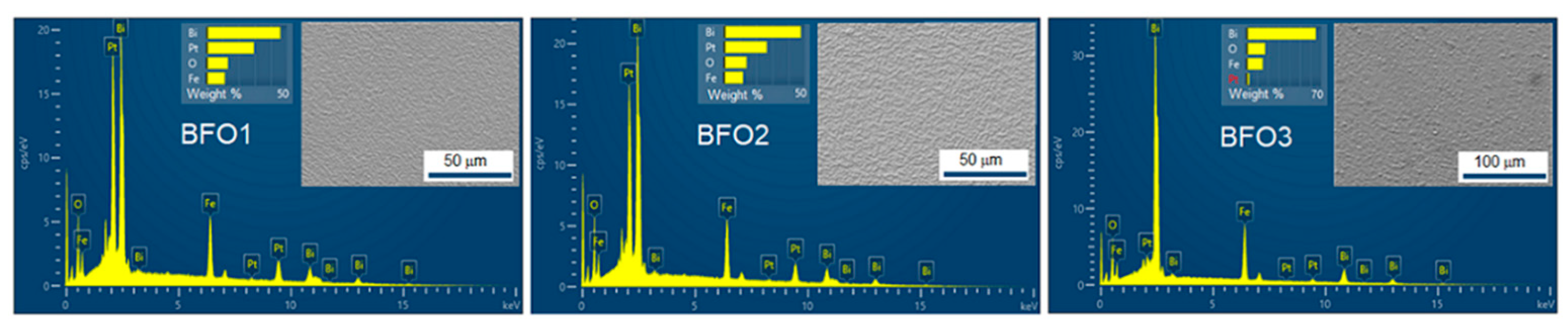
Figure 2.
(a) Observed (points) and calculated (red lines) XRD patterns of the studied BiFeO3 films (BFO1, BFO2, and BFO3). Traces of the secondary Bi25FeO39 and Bi2Fe4O9 phases are observed. (b) Raman spectra of the studied BiFeO3 thin films at room temperature. Black points are the experimental data; full fitting (red line) and Lorentzian curves (black lines) were used to fit and represent the individual Raman peaks corresponding to different phonon modes. (c) Williamson-Hall plots and (d) Raman shifts for the two A1(LO) modes of the BFO1, BFO2, and BFO3 films.
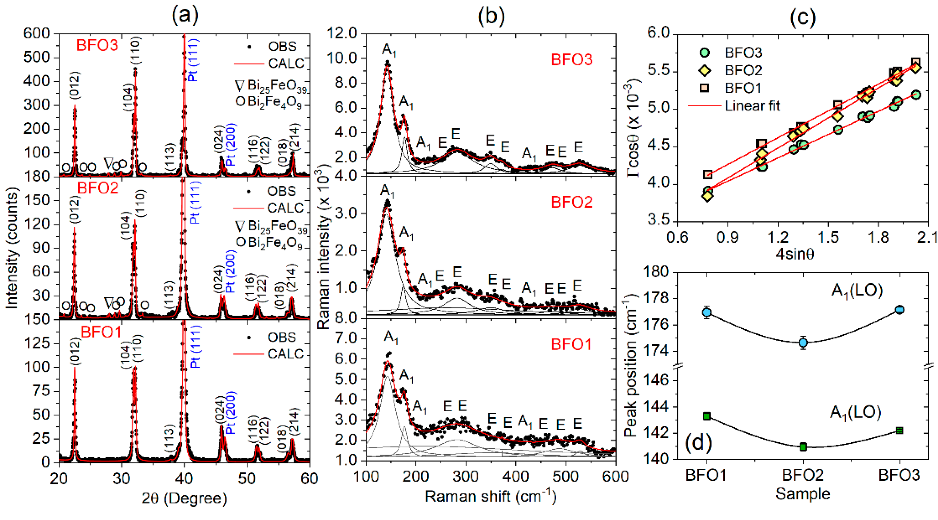
Figure 3.
X-ray photoelectron spectroscopy (XPS) spectra of (a) Bi 4f, (b) Fe 2p, and (c) O 1s for the studied BFO1, BFO2, and BFO3 thin films. Open circles in (b) and (c) are experimental data, while red lines are the fits.
Figure 3.
X-ray photoelectron spectroscopy (XPS) spectra of (a) Bi 4f, (b) Fe 2p, and (c) O 1s for the studied BFO1, BFO2, and BFO3 thin films. Open circles in (b) and (c) are experimental data, while red lines are the fits.
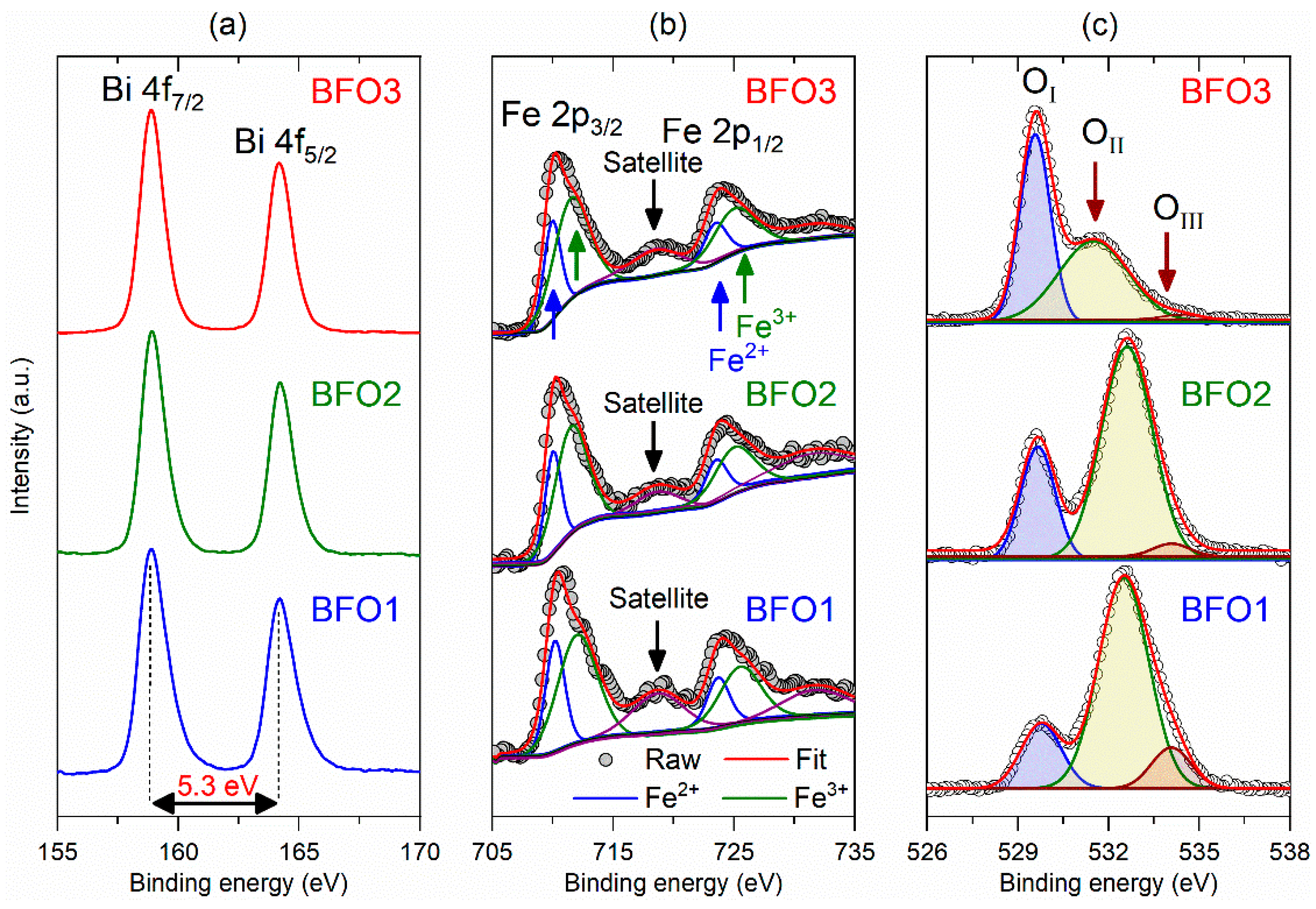
Figure 4.
Frequency dependence of (a) real () and (b) imaginary () dielectric permittivity, and (c) ac conductivity () of the studied BiFeO3 thin films (BFO1, BFO2, and BFO3) at room temperature. The red lines in (c) indicate theoretical fits using the Jonscher model. Temperature dependence of the (d) real and (e) imaginary dielectric permittivity at different frequencies of the studied BFO1, BFO2, and BFO3 thin films.
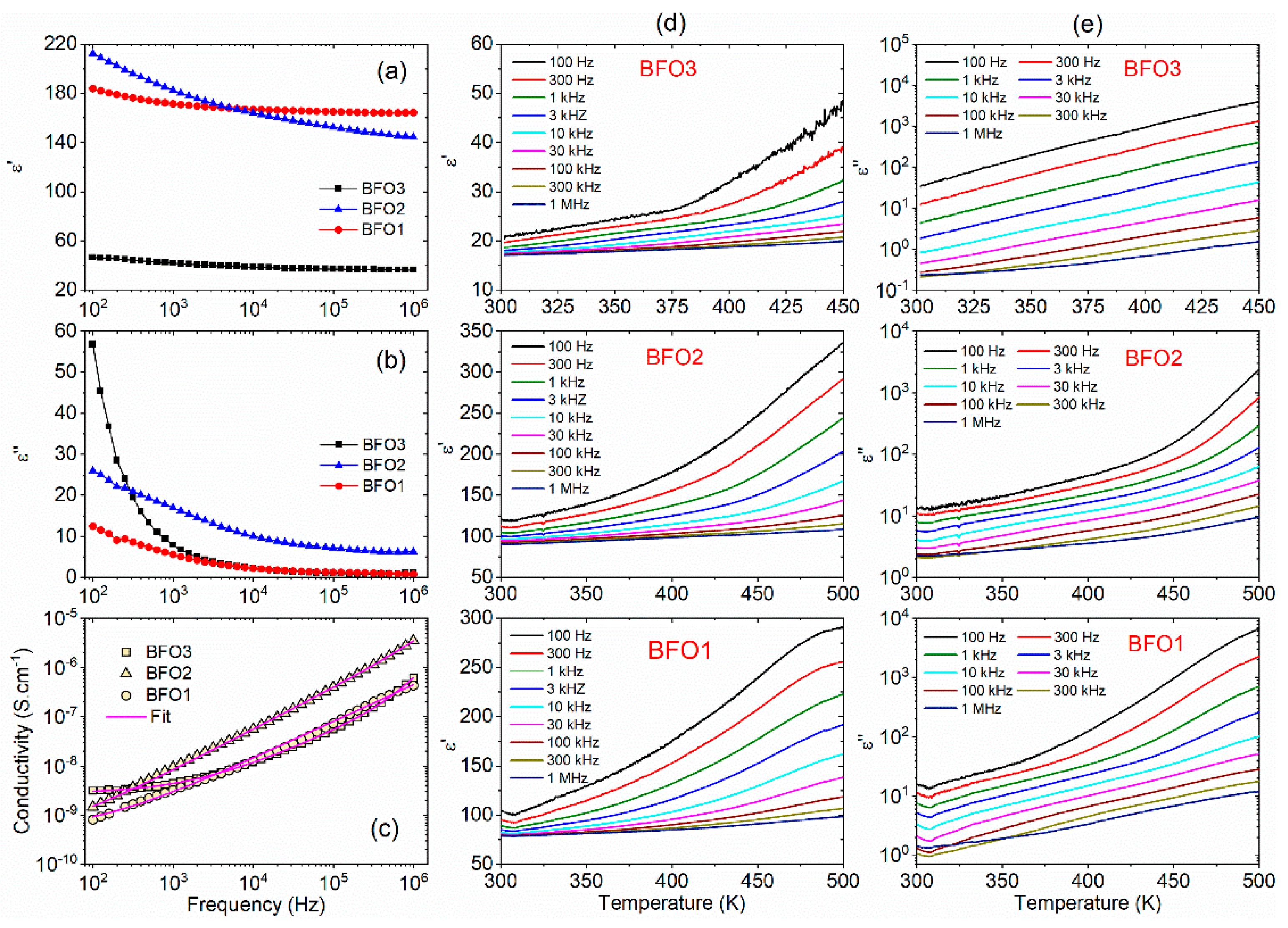
Figure 5.
Frequency dependence of the normalized imaginary parts () of impedance and () electric modulus for (a) BFO1, (b) BFO2, and (c) BFO3 thin films at selected temperature range.
Figure 5.
Frequency dependence of the normalized imaginary parts () of impedance and () electric modulus for (a) BFO1, (b) BFO2, and (c) BFO3 thin films at selected temperature range.
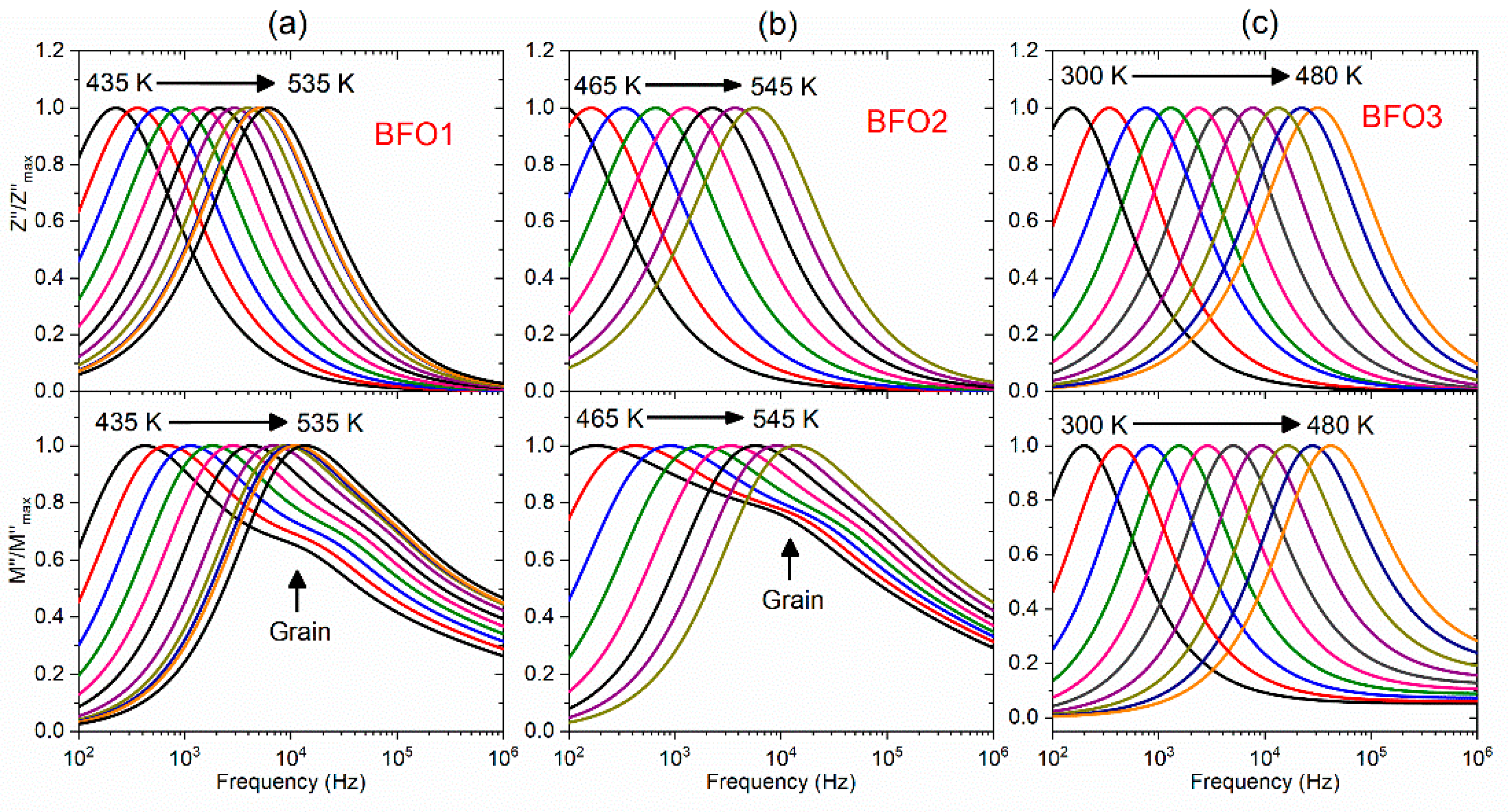
Figure 6.
Frequency dependencies of real () and imaginary () impedances for the (a) BFO1, (b) BFO2, and (c) BFO3 films and real () and imaginary () electric modulus for the (d) BFO1, (e) BFO2, and (f) BFO3 films at selected temperatures. Comparison of the and for (g) BFO1, (h) BFO2, and (i) BFO3 films as a function of the frequency at two different temperatures. In all cases, the lines are theoretical fits of Equations (1) to (4).
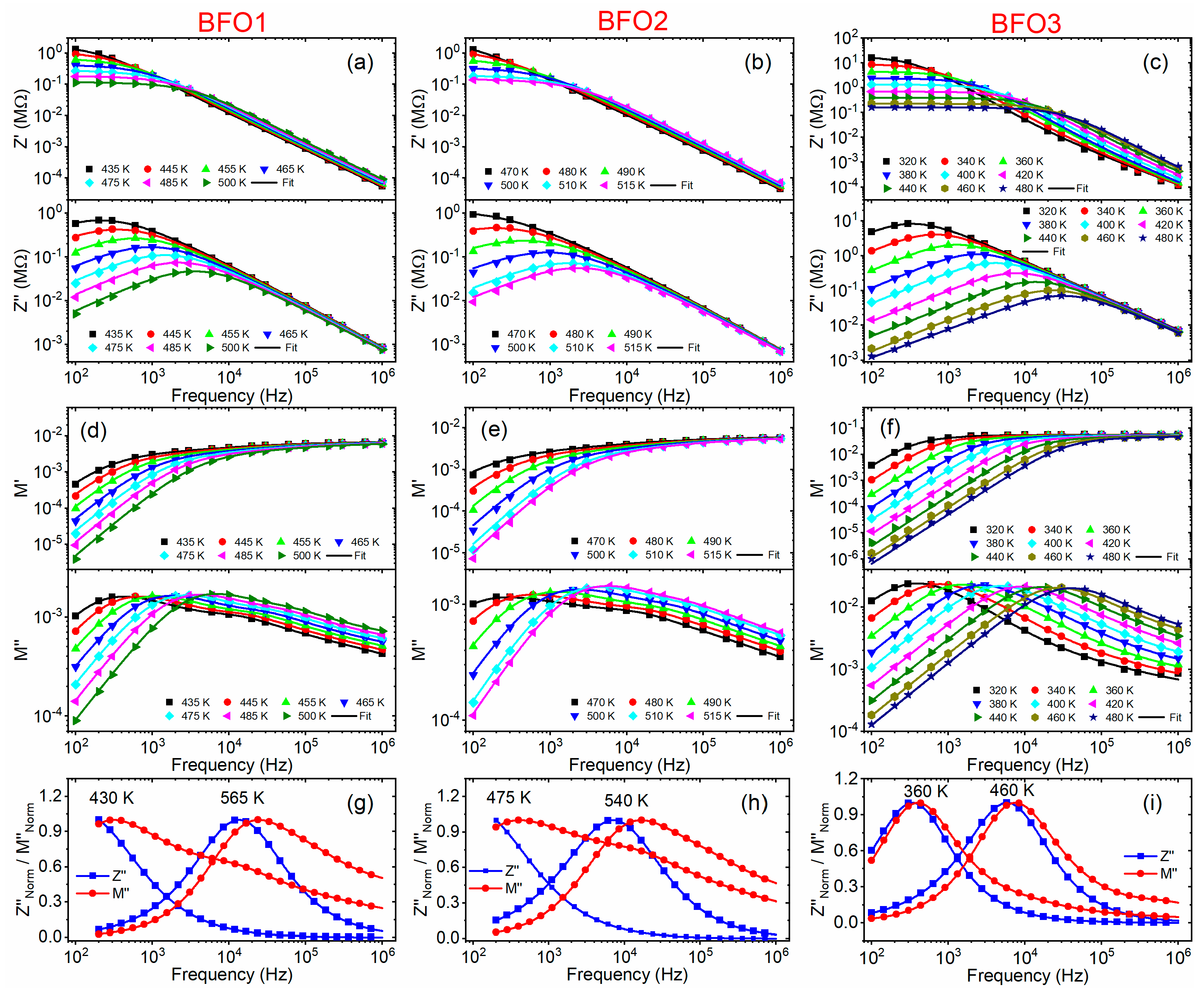
Figure 7.
DC conductivity as a function of the reciprocal temperature for the studied BFO1, BFO2, and BFO3 thin films, discriminating the grain and grain boundaries contributions. The results summarized in this figure were obtained from impedance and electric modulus theoretical fits in Figure 6. The inserted table summarizes the grain and grain boundary activation energies obtained from linear fits (red lines).
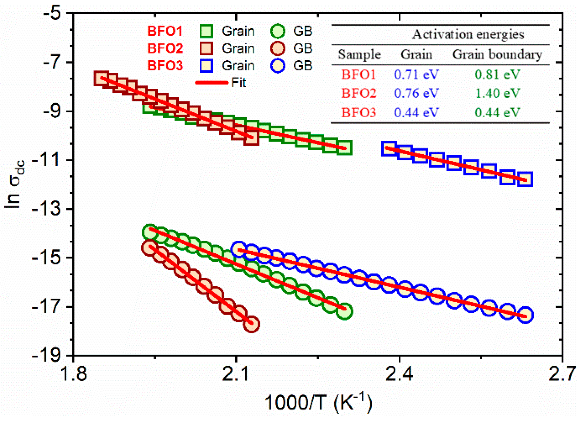
Figure 8.
(a) J-E leakage current curves and (b) J-E curves in log-log plots for the positive branch in (a) of the studied BFO1, BFO2, and BFO3 thin films at room temperature.
Figure 8.
(a) J-E leakage current curves and (b) J-E curves in log-log plots for the positive branch in (a) of the studied BFO1, BFO2, and BFO3 thin films at room temperature.
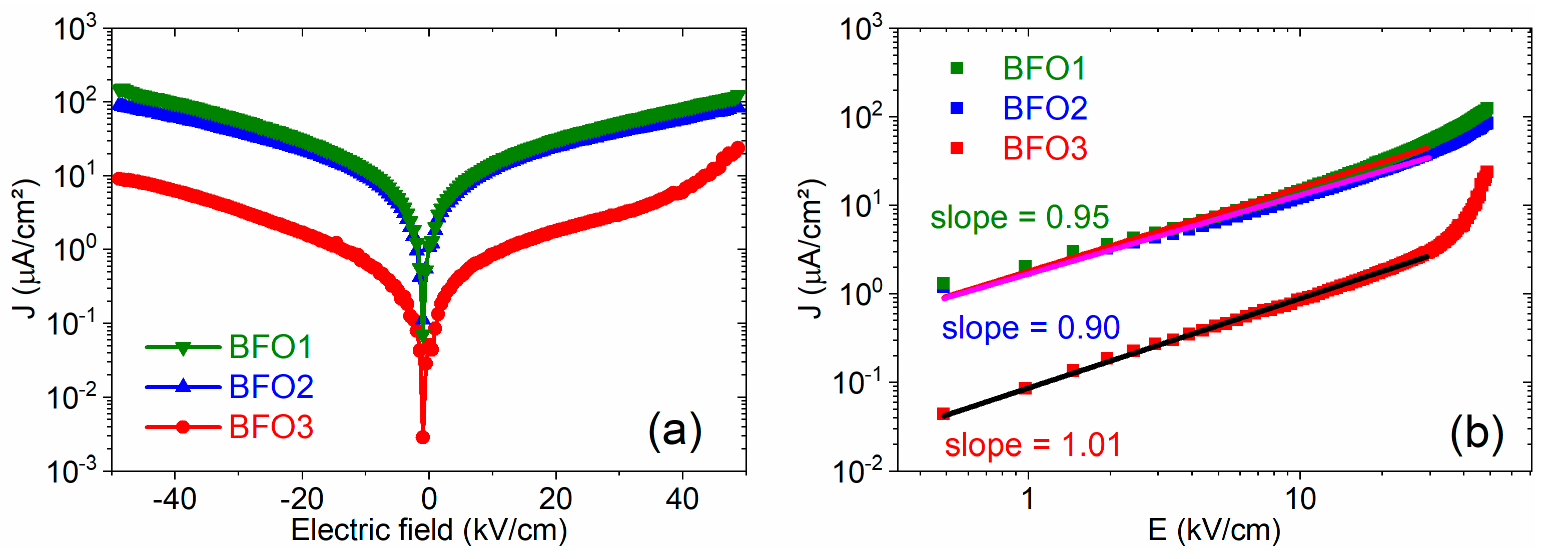
Figure 9.
Photocurrent density (JSC) of the studied BFO1, BFO2, and BFO3 thin films measured at zero bias under monochromatic green light (λ = 532 nm), under the regime “light on” and “light off” illumination.
Figure 9.
Photocurrent density (JSC) of the studied BFO1, BFO2, and BFO3 thin films measured at zero bias under monochromatic green light (λ = 532 nm), under the regime “light on” and “light off” illumination.
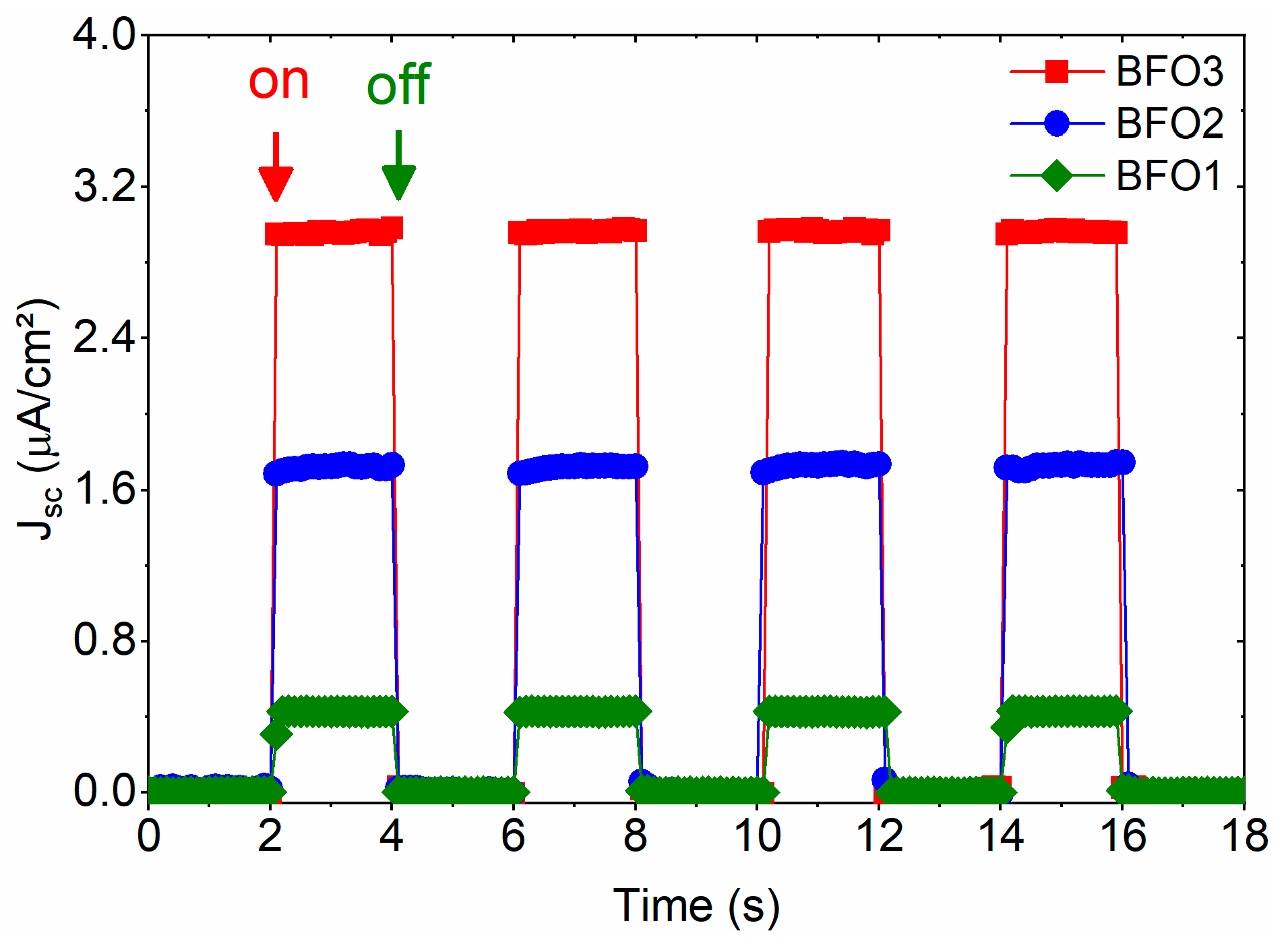
Figure 10.
(a) Magnetic hysteresis loops () taken at 300 K temperature and (b) at 5 K of the studied BFO1, BFO2, and BFO3 thin films. ZFC and FC magnetization curves as a function of temperature for the (c) BFO3 (at = 1 kOe), (d) BFO2 (at = 1 kOe), and (e) BFO1 (at = 3 kOe) films.
Figure 10.
(a) Magnetic hysteresis loops () taken at 300 K temperature and (b) at 5 K of the studied BFO1, BFO2, and BFO3 thin films. ZFC and FC magnetization curves as a function of temperature for the (c) BFO3 (at = 1 kOe), (d) BFO2 (at = 1 kOe), and (e) BFO1 (at = 3 kOe) films.
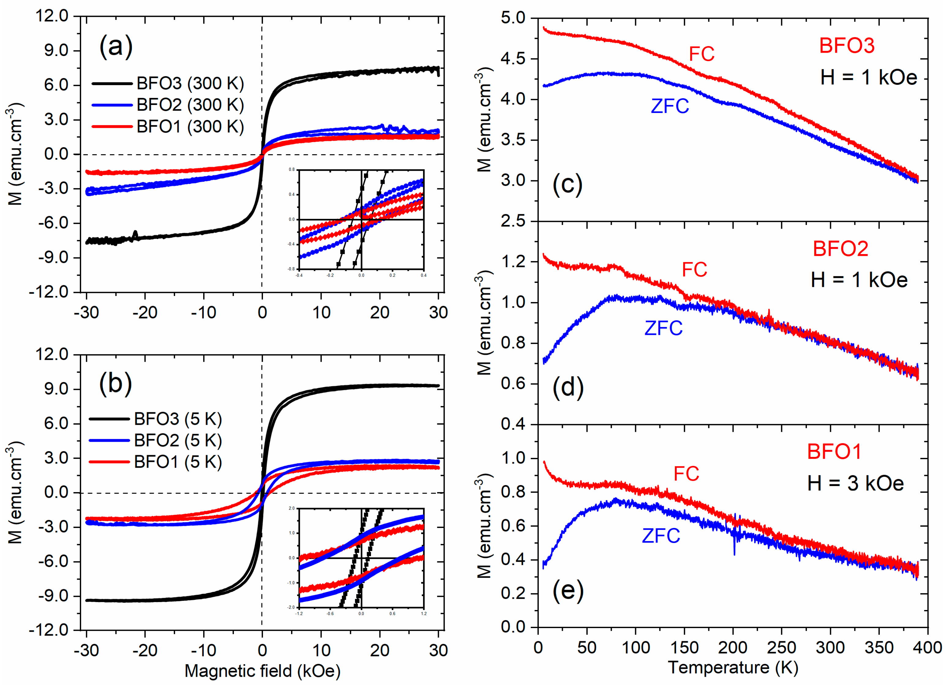

Table 1.
Summary of the conditions used for the preparation of the studied BiFeO3 thin films.
| Sample | Pyrolysis | Crystallization | Post annealing (in O2) |
| BFO1 | 300°C/60 min | 600°C/40 min (in air) | No |
| BFO2 | 300°C/60 min | 600°C/40 min (in air) | 600°C/5h |
| BFO3 | 360°C/10 min | 640°C/40 min (in O2) | No |
Table 2.
Atomic percentages of the elements in the studied BiFeO3 thin films obtained from the statistical analysis of the EDS data.
Table 2.
Atomic percentages of the elements in the studied BiFeO3 thin films obtained from the statistical analysis of the EDS data.
| Sample | Bi (atm%) | Fe (atm%) | O (atm%) | Bi/Fe | O/Bi | O/Fe |
| BFO1 | 17.0 ± 0.4 | 15.7 ± 0.4 | 67.3 ± 0.8 | 1.08 ± 0.08 | 4.0 ± 0.2 | 4.3 ± 0.2 |
| BFO2 | 17.5 ± 0.5 | 16.5 ± 0.6 | 66 ± 1 | 1.06 ± 0.07 | 3.8 ± 0.2 | 4.0 ± 0.2 |
| BFO3 | 21.5 ± 0.3 | 21.6 ± 0.3 | 57.0 ± 0.6 | 1.00 ± 0.02 | 2.7 ± 0.4 | 2.6 ± 0.1 |
Table 3.
Summary of structural parameters obtained from the Rietveld refinement of the XRD patterns of the studied BiFeO3 thin films.
Table 3.
Summary of structural parameters obtained from the Rietveld refinement of the XRD patterns of the studied BiFeO3 thin films.
| Sample | Lattice parameters |
Atomic positions |
x | y | z | R-factors |
| BFO1 | a = 5.569(9) Å | Bi3+ | 0.0000 | 0.0000 | 0.0000 | Rwp = 27.93% |
| c = 13.833(8) Å | Fe3+ | 0.0000 | 0.0000 | 0.2159 | Rp = 24.09% | |
| V = 371.68 Å3 | O2- | 0.4188 | 0.0223 | 0.9668 | = 1.017 | |
| BFO2 | a = 5.571(5) Å | Bi3+ | 0.0000 | 0.0000 | 0.0000 | Rwp = 26.96% |
| c = 13.849(7) Å | Fe3+ | 0.0000 | 0.0000 | 0.2115 | Rp = 22.96% | |
| V = 372.08 Å3 | O2- | 0.4450 | 0.0180 | 0.9503 | = 1.003 | |
| BFO3 | a = 5.571(5) Å | Bi3+ | 0.0000 | 0.0000 | 0.0000 | Rwp = 27.30% |
| c = 13.847(4) Å | Fe3+ | 0.0000 | 0.0000 | 0.2243 | Rp = 20.01% | |
| V = 372.26 Å3 | O2- | 0.4450 | 0.0180 | 0.9503 | = 1.937 |
Table 4.
Assignment and Raman modes obtained in the present work in comparison with results from the literature for BiFeO3 single crystals and epitaxial BiFeO3 thin films.
Table 4.
Assignment and Raman modes obtained in the present work in comparison with results from the literature for BiFeO3 single crystals and epitaxial BiFeO3 thin films.
| Symmetry | BFO1 (cm-1) | BFO2 (cm-1) | BFO3 (cm-1) | Crystal (cm-1) [27] | Film (cm-1) [28] |
| A1 | 144 | 141 | 142 | 140 | 135 |
| A1 | 177 | 175 | 177 | 173 | 172 |
| A1 | 216 | 215 | 217 | 220 | 218 |
| E | 261 | 261 | 261 | 265 | 266 |
| E | 282 | 282 | 283 | 279 | 277 |
| E | 349 | 349 | 350 | 350 | 350 |
| E | 372 | 372 | 372 | 371 | 365 |
| A1 | 430 | 430 | 425 | - | - |
| E | 474 | 474 | 473 | 471 | 465 |
| E | 487 | 487 | 489 | - | - |
| E | 529 | 528 | 528 | 550 | 548 |
Disclaimer/Publisher’s Note: The statements, opinions and data contained in all publications are solely those of the individual author(s) and contributor(s) and not of MDPI and/or the editor(s). MDPI and/or the editor(s) disclaim responsibility for any injury to people or property resulting from any ideas, methods, instructions or products referred to in the content. |
© 2026 by the authors. Licensee MDPI, Basel, Switzerland. This article is an open access article distributed under the terms and conditions of the Creative Commons Attribution (CC BY) license (http://creativecommons.org/licenses/by/4.0/).
Copyright: This open access article is published under a Creative Commons CC BY 4.0 license, which permit the free download, distribution, and reuse, provided that the author and preprint are cited in any reuse.


