
Submitted:
12 June 2023
Posted:
12 June 2023
You are already at the latest version
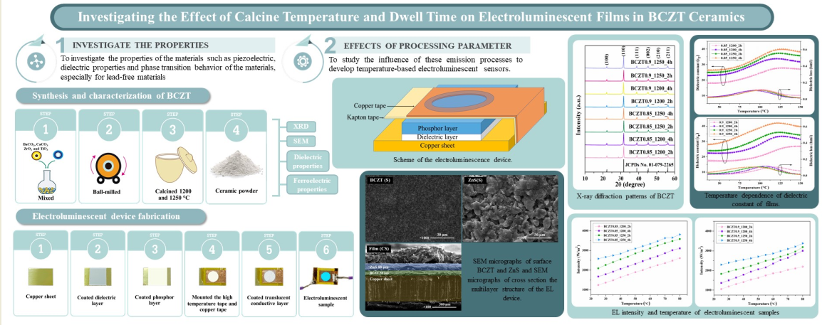
Abstract
Photoluminescent (PL) layers and electroluminescent (EL) systems have been extensively explored for constructing flat panels, screen monitors, and lighting systems. Due to their optical properties, our group is interested in the relationship between optical properties and dielectric constant is converted due to thermal change. In this study, we prepared a zinc sulfide (ZnS) fluorescent film on barium-calcium zirconium titanate ceramics. BCZT0.85 (Ba0.85Ca0.15Zr0.1Ti0.9O3) and BCZT0.9 (Ba0.9Ca0.1Zr0.1Ti0.9O3) were prepared using the solid-state reaction method for the dielectric layer. The BCZT powders were calcined at 1200 and 1250 °C and dwell times of 2 and 4h. The phase formation and microstructure characteristics were then determined using X-ray diffraction and scanning electron microscopy, respectively. The dielectric behavior and optical properties rela-tionship was then studied to determine the composition and optimal conditions for further use as thermal detectors in electric vehicle battery packs. All BCZT powders exhibited the tetragonal phase, which was confirmed by JCPDS No. 01-079-2265. The dielectric constant increased with increasing calcining temperature or dwell time. The dielectric properties showed the BCZT0.85 ceramic sintered had the maximum dielectric constant of 15342 at calcine temperature of 1250 °C for 4h. Therefore, in this study, this condition was optimal for preparing the dielectric film. The maximum dielectric constant film is 42. The electroluminescence intensity of the samples increased in a temperature-dependent manner, with the highest EL intensity at 80 °C. Moreover, the electroluminescence intensity value was enhanced with the increase of the dielectric constant. Our results show promise for developing applications for Opto-thermal sensors.
Keywords:
Photoluminescent
; Electroluminescent
; Spin coating method
1. Introduction
Chemical processes have been traditionally used to synthesize classic photoluminescent (PL) and electroluminescent (EL) materials. These materials exist in the form of sulfide, oxide, oxysulfide, nitride, and selenide compounds [1–6]. Using these powder precursors, thick PL and EL films are produced by screen printing or similar methods [1,7,8] comprising a highly efficient fluorescent system. Devices used for high-quality detection and inspection applications are subject to unwanted light scattering. Highly transparent thin film electroluminescent devices with a dielectric layer have optimal luminescent properties [9,10,11]. Luminescence can be achieved via excitation of photons (e.g., fluorescence), electrons (e.g., cathodoluminescence), and ions (e.g., ionoluminescence), or via the fabrication of electroluminescent systems [5,12–16]. In recent years, research focusing on systems made with inorganic materials has gained momentum due to their meager cost and availability. The performance of inorganic fluorescent films is temperature-dependent. Hence, this type of film has been used successfully in electric vehicle battery applications in the temperature range of 25 °C-80 °C. Moreover, the films can also withstand vibration. Due to these features, using inorganic films has several advantages including a reduction in the number of wires, saving electricity, and faster temperature checks of electric batteries during operation.
The general design of these devices is based on thin films of phosphor sulfide incorporated with a small fraction of transition metals [2,17,18]. At present, piezoelectric materials such as BaTiO3, Pb(ZrTi)O3, PbTiO3, Ba(ZrTi)O3 and KNaNbO3 are widely used in the electronic industry. Previous research has resulted in enhanced properties of piezoelectric materials, which can be used in various electronic devices [22]. The properties and behavior of piezoelectric materials can be improved by doping suitable elements at different atomic sites. Pb(Zr1-xTix)O3 (PZT)-base ceramics have long been known for their strong piezoelectric and dielectric characteristics. Numerous electronic applications, such as multilayer capacitors, sensors, transducers, and actuators, depend heavily on these ceramics [20-22]. However, the toxicity of lead oxide and its rapid vaporization during the sintering process at high temperature, makes PZT ceramics dangerous for the environment and human health [23]. Hence, research has focused on finding lead-free materials with suitable properties to replace lead-zirconate-titanate (PZT). Alternative materials such as barium-calcium zirconium titanate (BCZT) currently comprise the best choice for the development of dielectric and piezoelectric properties equaling or even surpassing those of lead. This is made possible by increasing the Curie temperature, dielectric coefficient, and mechanical quality coefficient. Using these materials to construct light emitting devices, including EL devices can improve emission efficiency. These bendable and flexible devices are widely used in illumination-related applications due to their narrow reflection behavior [24].
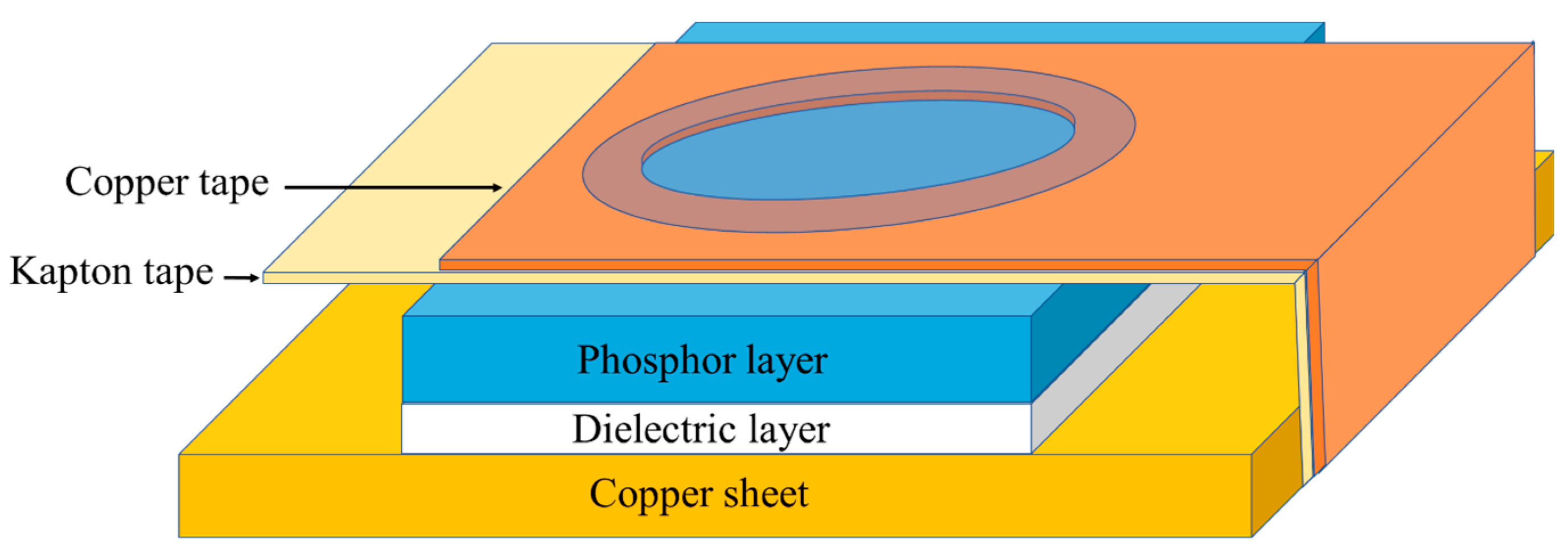
This study focused on electroluminescent device fabrication and their properties. We firstly prepared barium-calcium zirconium titanate ceramics powder to use as the dielectric layer. BCZT0.85 (Ba0.85Ca0.15Zr0.1Ti0.9O3) and BCZT0.9 (Ba0.9Ca0.1Zr0.1Ti0.9O3) were prepared using the solid-state reaction method. The BCZT powders were calcined at 1200 and 1250 °C at dwell times of 2 and 4h. We then constructed a film consisting of four main layers: an electrode layer, a dielectric layer, a phosphor layer, and a translucent conductive layer. To stimulate electroluminescence of the cations of the phosphor layer through the host-lattice energy transfer activation mechanism, the dielectric value of the dielectric layer was changed [25,26,27]. Adjusting of the dielectric value according to temperature resulted in corresponding changes in fluorescence, allowing for the development of a thin and small temperature-measuring device.
2. Materials and Methods
2.1. Synthesis and Characterization of BCZT
The Ba0.85Ca0.15Zr0.1Ti0.9O3 and Ba0.9Ca0.1Zr0.1Ti0.9O3 ceramics powder was prepared by using the solid-state reaction method. The starting materials were BaCO3 (99%, Sigma–Aldrich), CaCO3 (98.5–100.5%, Sigma–Aldrich), ZrO2 (99%, Sigma–Aldrich), and TiO2 (99%, Sigma–Aldrich) oxide powders. The oxide powders were weighed according to stoichiometric formulae, mixed using ethanol as a solvent and ball-milled for 24h. The slurry was dried at 100 °C for 24h and sieved. The mixed compounds were calcined at different temperatures and dwell times at 1200 and 1250 °C for 2 and 4h, respectively. Subsequently, the powder was uniaxially pressed into green pellets 10 mm in diameter and 1 mm in thickness at a one-ton compression. Finally, the samples were sintered at 1450 °C for 4h. The phase formation of ceramics powder was observed by x-ray diffraction (XRD). Scanning electron microscopy (SEM) and the intercept method were used to examine the microstructure and grain size, respectively. To characterize the dielectric and ferroelectric properties, the surfaces of the sintered samples were polished and coated with silver paste on both sides to serve as electrodes.
2.2. Preparation and Characterization of EL Film
The electroluminescent films consisted of an electrode, dielectric, phosphor, and translucent conductive layers. The films were prepared by using the spin coating method. In the first layer, the dielectric film was prepared by mixing BCZT powder and alkyd resin binder, deposited on a copper sheet and spread out. In the phosphor layer, ZnS powder was mixed with binder and deposited over the dielectric layer. Finally, the translucent conductive layer was prepared by spin coating over the phosphor layer. Each layers was individually dried at room temperature for 30 minutes before coating the next layer.
The BCZT0.85 and BCZT0.9 were synthesized from Ba0.85Ca0.15Zr0.1Ti0.9O3 and Ba0.9Ca0.1Zr0.1Ti0.9O3 systems, respectively, each condition was calcined at different temperatures and dwell times at 1200 and 1250 °C for 2 and 4h, respectively (Table 1).
Figure 1.
Scheme of the electroluminescence device.
3. Results and Discussion
3.1. XRD Phase Analysis of BCZT Powders
In this work, BCZT ceramics were synthesized using the solid-state reaction method. Phase formation of the BCZT powder was analyzed by using XRD (Figure 2 and Figure 3). The samples were calcined at different temperatures and dwell times at 1200 °C for 2h, 1200 °C for 4h, 1250 °C for 2h and 1250 °C for 4h. Based on the XRD patterns for 2θ = 29, the sample calcined at 1200 °C for 2h had an unidentified phase. However, upon increasing the calcining temperature or dwell time to 1200 °C for 4h, 1250 °C for 2h and 1250 °C for 4h, the unidentified phase disappeared. The resulting XRD patterns had a pure perovskite without a secondary peak of impurity phase [26,27]. Regarding the expanded XRD patterns for 2θ = 36°–49°, the split of the single peaks of (111) reflections was observed at 2θ ~ 38° to 40° and single peak of (002) reflection at 2θ ~ 44° to 46° in all samples used in this study [30]. This suggested that all the samples had a of pseudo-cubic phase [31].
3.2. Microstructure Analysis of BCZT Ceramics
Figure 4 and Figure 5 display SEM micrographs of the sintered surface of BCZT0.85 and BCZT0.9 ceramics at 1450 °C for 4h. The grain morphology did not change significantly in neither of these ceramics. The grain shapes of all conditions had irregular polyhedral shapes and were non-homogeneous. In this study, the calcining temperature had a significant effect on the microstructure of BCTZ ceramics. Specifically, the grain size of BCZT ceramics increased with increasing calcining temperature and dwell time. Calcining at 1200 °C for 2h was not enough for crystal formation, resulting in small grain size. Increasing both the dwell time and calcining temperature, resulted in large grain size distribution, a finding which was confirmed by SEM. Moreover, the grain size correlated with LV intensity; as grain size increased, the light intensity also increased. which corresponded to the results of the light intensity test.
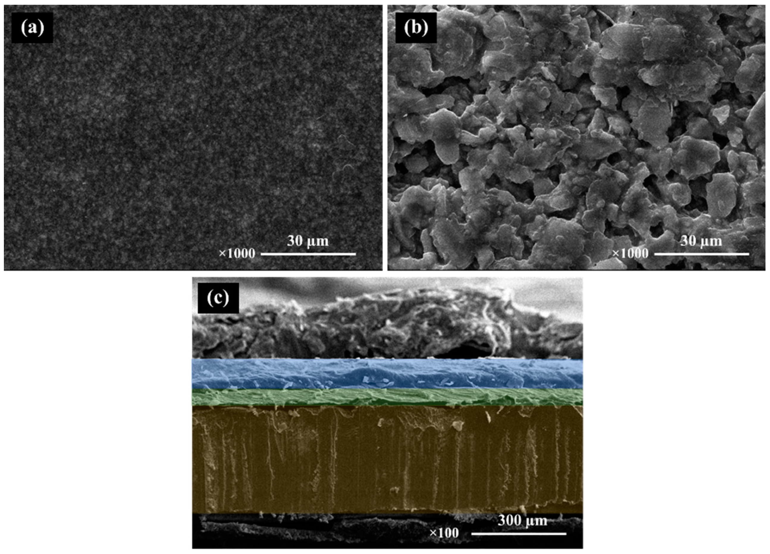
shows an SEM image of the BCZT and ZnS surface and a cross-section micrograph of a sandwiched electroluminescent device. The former shows the significantly larger particle size of ZnS when compared to BCZT, while the cross-section depicts the device’s uniform microstructure along the entirety of its surface. The stacking order of the EL device from bottom to top comprises a copper sheet, a BCZT layer, and a ZnS layer, all of which are clearly shown in the micrograph. Additionally, this device supports compactness of the film microstructure and the planar phosphor and dielectric layer interfaces. These microstructural features confer a high optical quality to the whole structure which, as represented by electroluminescent spectra in Figures 16 and 17, glows in the visible spectrum.
Figure 4.
SEM micrographs of surface Ba0.85Ca0.15Zr0.1Ti0.9O3.
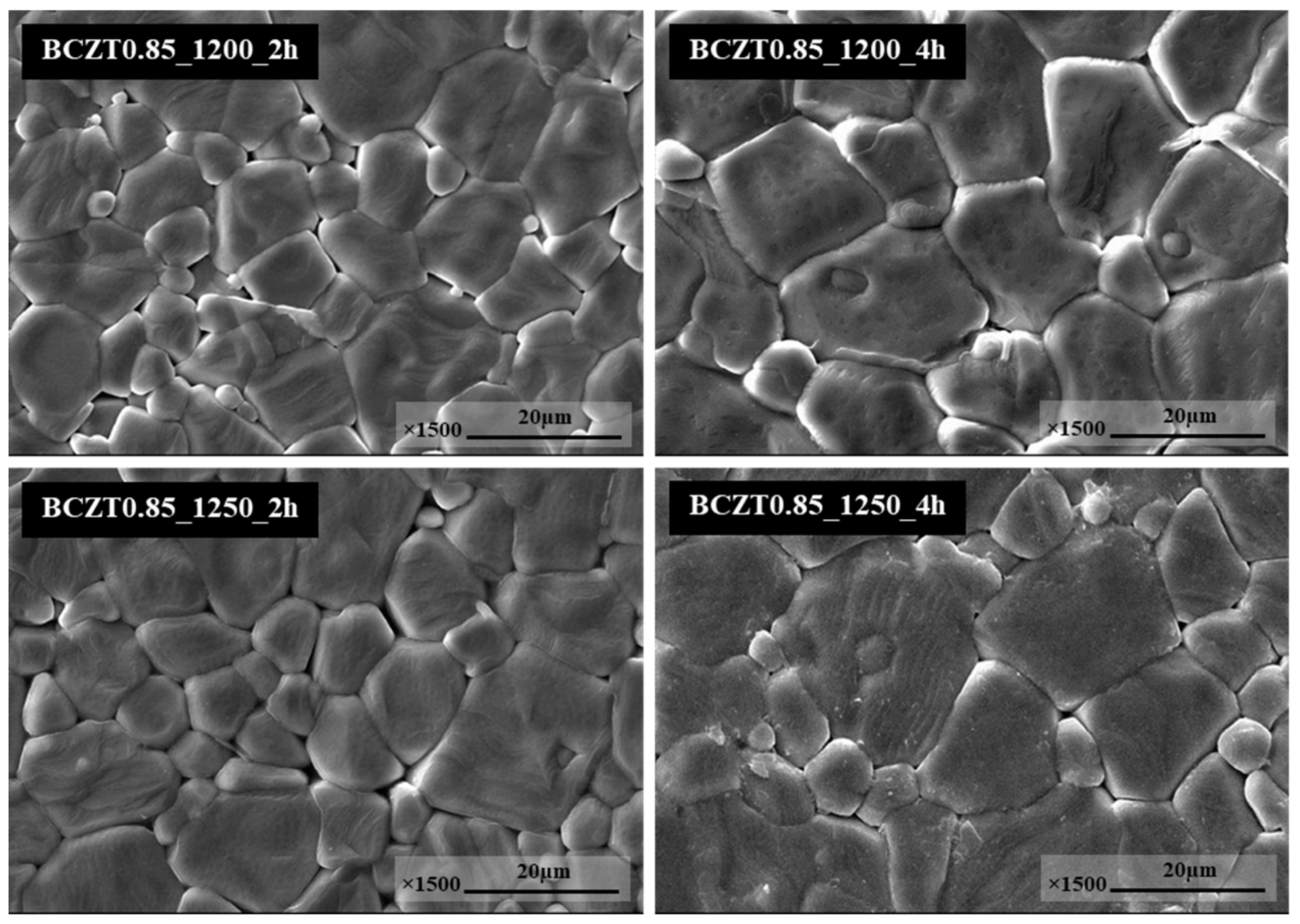
Figure 5.
SEM micrographs of surface Ba0.9Ca0.1Zr0.1Ti0.9O3.
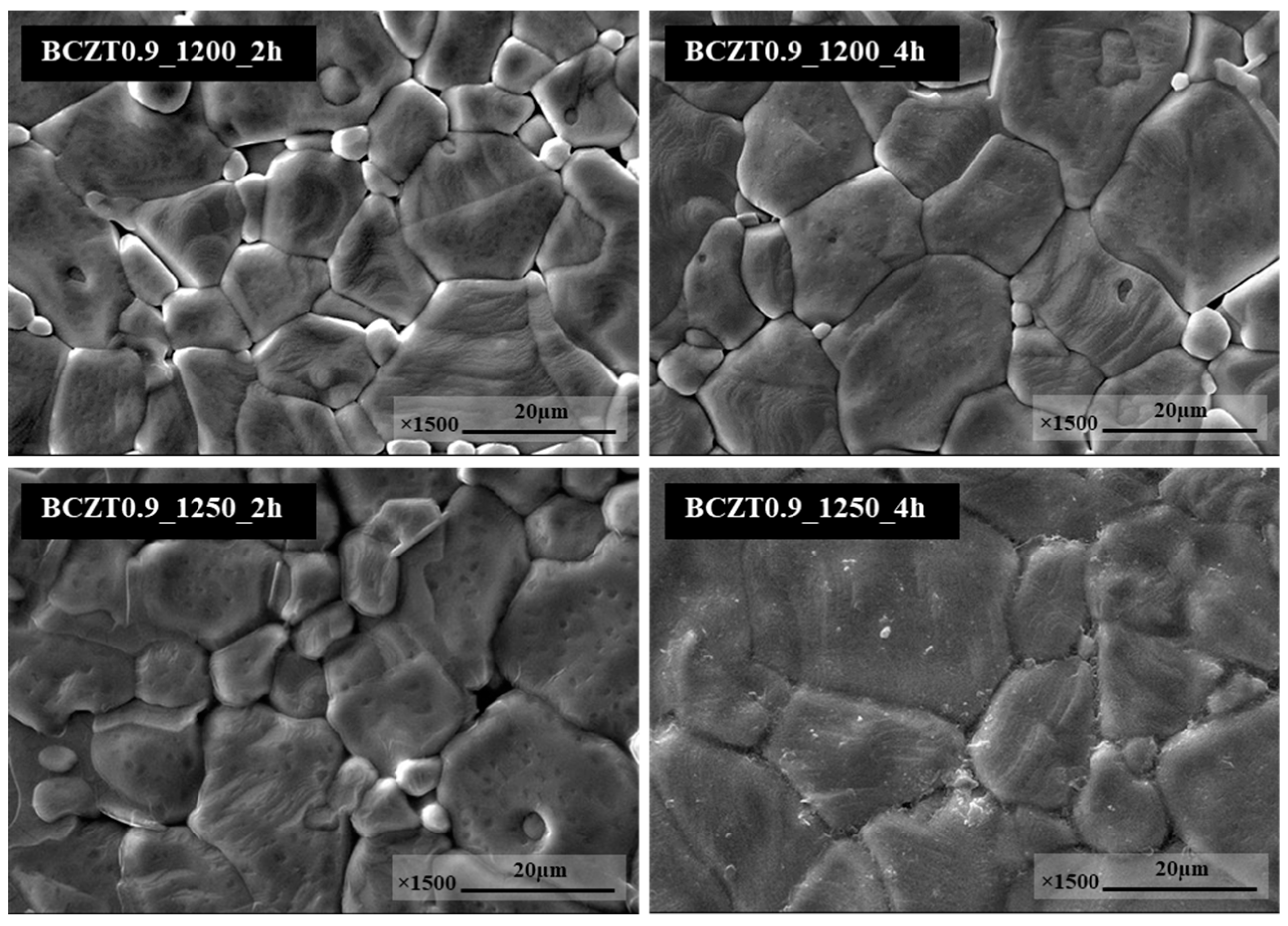
Figure 6.
SEM micrographs of surface BCZT film (a), ZnS film (b) and SEM micrographs of cross section the multilayer structure of the EL device (c).
Figure 6.
SEM micrographs of surface BCZT film (a), ZnS film (b) and SEM micrographs of cross section the multilayer structure of the EL device (c).
3.3. Electrical Properties of BCZT Ceramics
The dielectric constant (εr) and dielectric loss (tanδ) of ceramic samples measured at room temperature as a function of frequency are displayed in Figure 7 and Figure 8. The dielectric constant and dielectric loss of the Ba0.85Ca0.15Zr0.1Ti0.9O3 ceramics calcined at different temperatures and dwell times were compared. The maximum dielectric constant of the BCZT0.85_1250_2h sample at 1 kHz was 3326, while that of the BCZT0.85_1250_4h sample was 2910 (Figure 7). The maximum dielectric constant at 1 kHz of the BCZT0.9_1250_4h sample was 2905, while the minimum dielectric constant at 1 kHz was 2368 for the BCZT0.9_1200_4h sample. Overall, the dielectric constant of all Ba0.85Ca0.15Zr0.1Ti0.9O3 ceramic samples was higher than all Ba0.9Ca0.1Zr0.1Ti0.9O3 ceramic samples. The temperature-related dielectric shift impacts light intensity, which is helpful for measuring light intensity versus temperature.
The relationship between dielectric properties and temperature from 30 °C to 250 °C of Ba0.85Ca0.15Zr0.1Ti0.9O3 and Ba0.9Ca0.1Zr0.1Ti0.9O3 is shown in Figure 9 and Figure 10 respectively. The maximum dielectric peak of all ceramics exhibited only slight variation with frequency. The maximum dielectric constant (εr) of Ba0.85Ca0.15Zr0.1Ti0.9O3 and Ba0.9Ca0.1Zr0.1Ti0.9O3 ceramics at Curie temperature increased modestly with increasing calcine temperature and dwell time ranging from 11314–15341 and 8828.78–13455.9 (measured at 1 kHz), respectively. Dielectric loss (tanδ) showed similar behavior to that of the dielectric constant. No significant change was observed with increasing frequency, calcine temperature or dwell time. The lowest tanδ value of all samples measured between 30 and 250 °C was 0.01807. Hence, the calcine temperature and dwell time had an effect on the dielectric loss of BCZT ceramics. Furthermore, the Curie temperature (TC) of ceramics, which ranged from 95 to 100 °C, did not significantly change with increased calcine temperature and dwell time.
The hysteresis loop confirmed the ferroelectric properties of the BCZT ceramics. The loops between polarization (P) and an applied electric field (E) showed saturation polarization when an electric field of ∼5 kV/mm was used (Figure 11a). Plots of the ferroelectric parameters such as remnant polarization (Pr) and coercive field (Ec) as a function of different calcine temperature and dwell time of Ba0.85Ca0.15Zr0.1Ti0.9O3 and Ba0.9Ca0.1Zr0.1Ti0.9O3 ceramics are shown in Figure 11b. The calcine temperature and dwell time had no significant effect on the Pr and Ec values. The highest Pr value was found in the sample BCZT0.9_1250_4h, while an Ec value of 3.4921 kV/cm was obtained for the BCZT0.85_1250_4h sample.
3.4. Electrical Properties of BCZT Films
To characterize the electrical properties of BCZT film, a sample was prepared by spin coating BCZT powder with a binder on copper sheet. Subsequently, a silver electrode was coated with a BCZT layer. The εr and tanδ at room temperature as a function of frequency are displayed in Figure 12 and Figure 13. Both calcine temperature and dwell time affected the dielectric properties of BCZT ceramics. The εr value increased with increasing calcine temperature and dwell time. The εr values of film BCZT0.85 samples were in the range of 23.064–29.672, while those of film BCZT0.9 samples ranged from 23.618–32.171. The BCZT0.85_1250_2h sample had the highest tanδ at 1 kHz. Other samples showed tanδ less than 0.018. In general, the film BCZT0.9 sample had higher dielectric constant than the film BCZT0.85. This could be a result of the calcined temperature, which is associated with changes in the microstructure of the ceramic.
The temperature dependence of the dielectric constant and dielectric loss at a frequency of 10 kHz is presented in Figure 14 and Figure 15. The dielectric constants of the BCZT0.85 and BCZT0.9 were compared using the graph with calcined temperatures and dwell times of 1200 °C at 2-4h and 1250 °C at 2-4h, respectively. Both the calcine temperature and dwell time had a significant effect on the dielectric constant. The dielectric constant at Curie temperature (TC) increased with increasing calcine temperature and dwell time. The maximum value was 42, which was the calcined temperature at 1250 °C and dwelling at 4h for the BCZT0.9 sample. The TC of the film BCZT samples was in the range of 120–147 °C.
3.5. Electroluminescent Properties
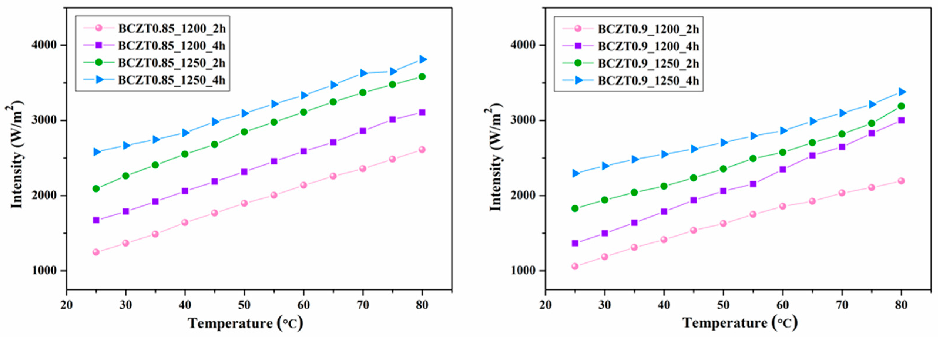
Figure 16 and Figure 17 present the electroluminescent spectra of the EL devices with various calcine temperatures and dwell times of BCZT0.85 or BCZT0.9 on the dielectric layer. The blue electroluminescence emission from all devices mentioned above had peak intensity at a wavelength of 499–506 nm and exhibited a full width half maximum (FWHM) of 83-84 nm, when heated at 80 °C. By comparison, the light intensity of BCZT in the dielectric layer along with the electroluminescence intensity increased when the calcining temperature and dwell time increased. The electroluminescence intensity of the EL devices with BCZT0.85 coating on the dielectric layer ranged from 2611 to 3812 W/m2, whereas that of the dielectric layer coated with BCZT0.9 was between 2178 and 3358 W/m2. Moreover, the electroluminescence intensity increased in a temperature-dependent manner. Hence, manipulating temperature and dielectric constant leads to improved fluorescence, which could be efficiently used in the field of opto-thermal sensors.
Figure 16.
Electroluminescent (EL) spectra for the devices with different calcine temperature and dwell time of Ba0.85Ca0.15Zr0.1Ti0.9O3 on dielectric layer.
Figure 16.
Electroluminescent (EL) spectra for the devices with different calcine temperature and dwell time of Ba0.85Ca0.15Zr0.1Ti0.9O3 on dielectric layer.
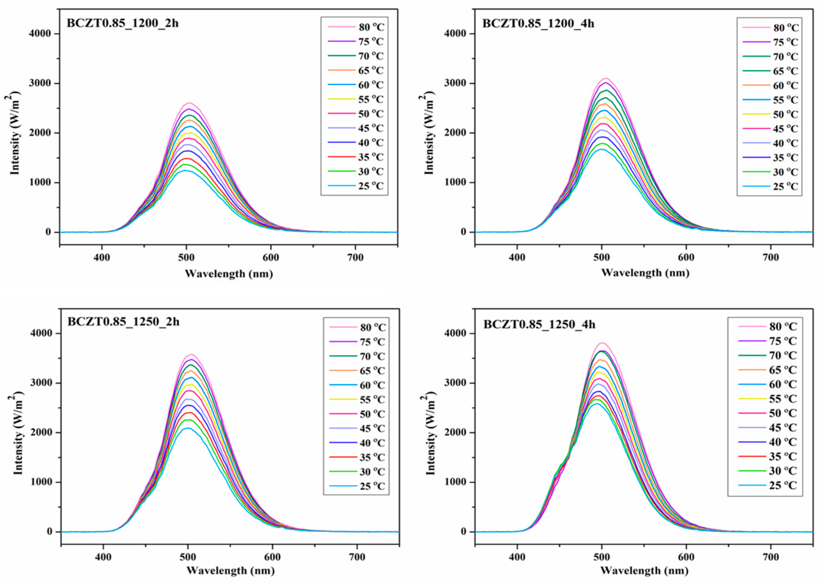
Figure 17.
Electroluminescent (EL) spectra for the devices with different calcine temperature and dwell time of Ba0.9Ca0.1Zr0.1Ti0.9O3 on dielectric layer.
Figure 17.
Electroluminescent (EL) spectra for the devices with different calcine temperature and dwell time of Ba0.9Ca0.1Zr0.1Ti0.9O3 on dielectric layer.
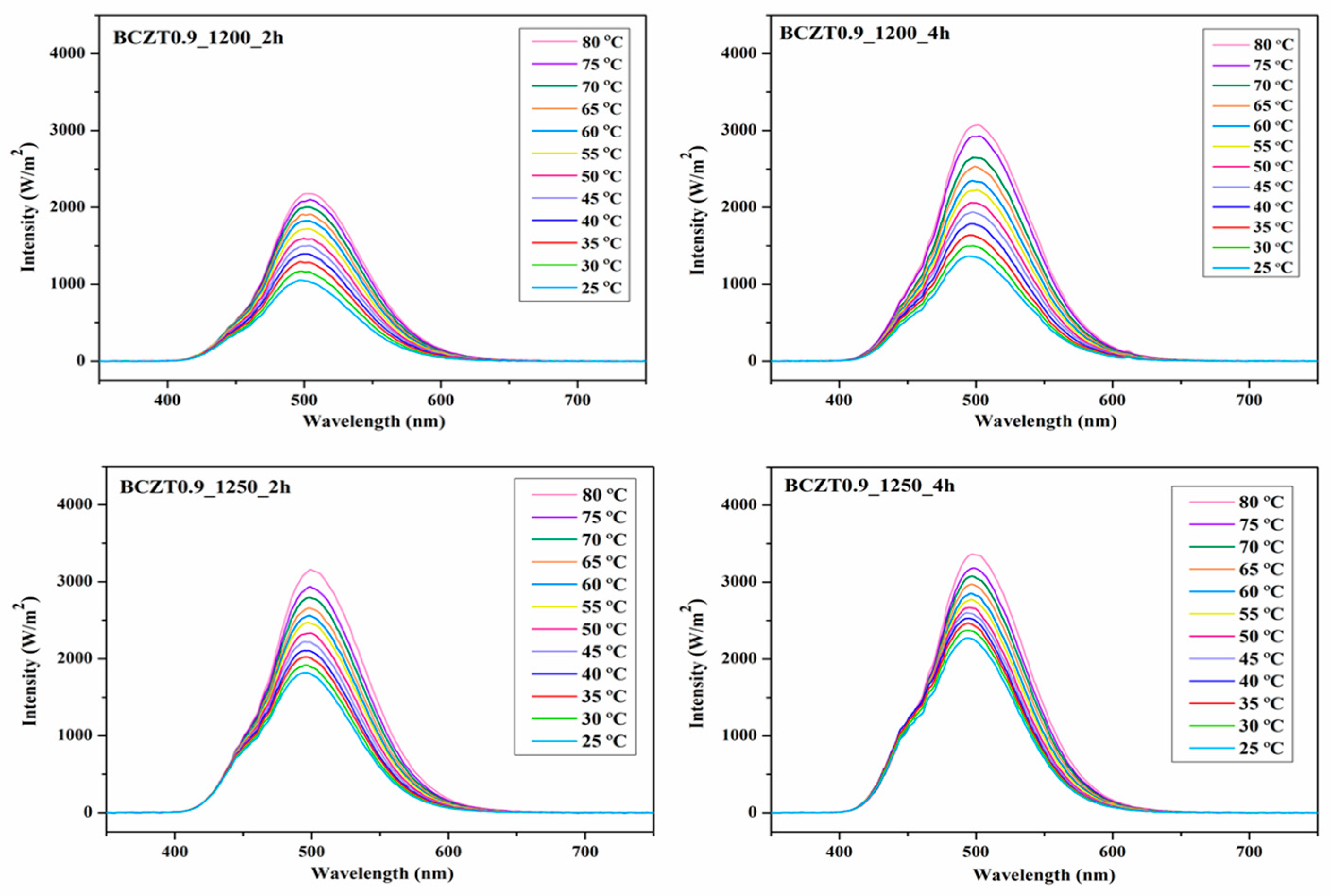
Figure 18.
EL intensity and temperature of electroluminescent samples.
The device created in our lab emits blue light at about 503 nm. The Commission Internationale de L’éclairage (CIE) coordinates are (x = 0.1538, y = 0.2015) at 25o C. At 80 °C, the CIE coordinates are (x = 0.1640, y = 0.2724) (see Figure 19). Figure 20 shows a photo image of the EL device with BCZT0.85_1250_4h on the dielectric layer.
4. Conclusions
In this work, we have applied a variation of the spine coating procedure to prepare electroluminescent films consisting of four main layers: an electrode layer, a dielectric layer, a phosphor layer and a translucent conductive layer. The Ba0.85Ca0.15Zr0.1Ti0.9O3 and Ba0.9Ca0.1Zr0.1Ti0.9O3 ceramics were exposed to different calcine temperature and dwell times on the dielectric layer of electroluminescent films. This methodology has provided evidence that different calcine temperatures and dwell times of dielectric powder have an effect on ceramic microstructure and dielectric properties of ceramics and films, besides affecting the intensity of luminescent emission. All of the BCZT powders exhibited the tetragonal phase, which was confirmed by JCPDS No. 01-079-2265 and the particle sizes of BCZT increased with increasing calcination time from 2 to 4h. The dielectric constant (εr) at Curie temperature of BCZT ceramics and films tended increased modestly with increasing calcine temperature and dwell time. The electroluminescence intensity increased when the calcine temperature and dwell duration rose. Moreover, the EL intensity value tended to rise as the temperature rose. This remarkable performance demonstrates the feasibility of using the electroluminescent film as Ba0.85Ca0.15Zr0.1Ti0.9O3 calcine at 1250 °C for 4h on the dielectric layer using the spin coating method technique for the entire fabrication of electroluminescent multilayer devices.
Author Contributions
Conceptualization, M.K. and S.E.; methodology, M.K. and S.E.; resources and material manufacturing M.K., S.E., K.P., O.K. and U.I.; investigation, M.K., S.E.and K.P.; writing—original draft preparation, M.K.; and data analysis, M.K., S.E., K.P., T.T., O.K. and U.I. All authors contributed to writing—review and editing. All authors have read and agreed to the published version of the manuscript.
Funding
This research was funded by the National Research Council of Thailand (NRCT), grant number NRCT-RSA63004-02.
Institutional Review Board Statement
Not applicable
Informed Consent Statement
Not applicable
Data Availability Statement
Not applicable
Acknowledgments
This work is a part of the project entitled “Enhancement of dielectric properties of lead free BCZT Ceramics Powder for Electroluminescence applications, NRCT-RSA63004-02 which is supported by the National Research Council of Thailand (NRCT).
Conflicts of Interest
The authors declare no conflict of interest.
References
- Barrow, W.A. Electroluminescent Displays. In The Measurement Instrumentation and Sensors Handbook; Webster, G.J., Ed.; CRC Press: Boca Raton. FL, USA, 1999; pp. 2449–2461. [Google Scholar]
- Rack, P.D.; Holloway, P.H. The structure device physics and material properties of thin film electroluminescent displays. Mater. Sci. Eng. R Rep. 1998, 21, 171–219. [Google Scholar] [CrossRef]
- Minami, T. Oxide thin-film electroluminescent devices and materials. Solid State Electron. 2003, 47, 2237–2243. [Google Scholar] [CrossRef]
- King, C.N. Electroluminescent displays. J. Vac. Sci. Technol. 1996, A 14, 1729–1735. [Google Scholar] [CrossRef]
- Kitai, A. Luminescent Materials and Applications; John Wiley & Sons Ltd: Chichester, England, 2008; pp. 223–248. [Google Scholar]
- Korsunska, N.; Borkovska, L.; Khomenkova, L.; Sabov, T.; Oberemok, O.; Dubikovsky, O.; Zhuchenko, Z.Y.; Zolotovsky, A.; Demchenko, I.N.; Syryanyy, Y.; Guillaume, C.; Labbe, C.; Portier, X. Redistribution of Tb and Eu ions in ZnO films grown on different substrates under thermal annealing and its impact on Tb-Eu energy transfer. Appl. Surf. Sci. 2020, 528, 146913. [Google Scholar] [CrossRef]
- Srivastava, S.; Behera, S.K.; Nayak, B.B. Optimization and photoluminescence behaviour of terbium doped YBO3 phosphors. Opt. Mater. 2020, 107, 110178. [Google Scholar] [CrossRef]
- Cui, R.; Liu, W.; Zhou, L.; Zhao, X.; Jiang, Y.; Cui, Y.; Zhu, Q.; Zheng, Y.; Zhang, H. Green phosphorescent organic electroluminescent devices with 27.9% external quantum efficiency by employing a terbium complex as a co-dopant. J. Mater. Chem. 2019, C 7, 7953–7958. [Google Scholar] [CrossRef]
- Chase, E.W.; Hepplewhite, R.T.; Krupka, D.C.; Kahng, D. Electroluminescence of ZnS lumocen devices containing rare-earth and transition-metal fluorides. J. Appl. Phys. 1969, 40, 2512–2519. [Google Scholar] [CrossRef]
- Krasnov, A.N. Electroluminescent displays: history and lessons learned. Displays. 2003, 24, 73–79. [Google Scholar] [CrossRef]
- Chen, H.W.; Lee, J.H.; Lin, B.Y.; Chen, S.; Wu, S.T. Liquid crystal display and organic light-emitting diode display: present status and future perspectives. Light Sci. Appl. 2018, 7, 17168. [Google Scholar] [CrossRef]
- Hoppe, H.A. Recent developments in the field of inorganic phosphors. Angew. Chem. Int. Ed. 2009, 48, 3572–3582. [Google Scholar] [CrossRef] [PubMed]
- Li, L.; Wang, S.; Mu, G.; Yin, X.; Yi, L. Multicolor light-emitting devices with Tb2O3 on silicon. Sci. Rep. 2017, 7, 42479. [Google Scholar] [CrossRef]
- Ferrer, F.J.; Gil-Rostra, J.; Gonz’ alez-Elipe, A.R.; Yubero, F. Colorimetric energy sensitive scintillator detectors based on luminescent multilayer designs. Sens. Actuators Phys. 2018, 272, 217–222. [Google Scholar] [CrossRef]
- Gil-Rostra, J.; Ferrer, F.J.; Martín, I.R.; Gonz´ alez-Elipe, A.R.; Yubero, F. Cathode and ion-luminescence of Eu:ZnO thin films prepared by reactive magnetron sputtering and plasma decomposition of non-volatile precursors. J. Lumin. 2016, 178, 139–146. [Google Scholar] [CrossRef]
- Sun, J.M.; Skorupa, W.; T. Dekorsy, Helm, M.; Rebohle, L.; Gebel, T. Bright green electroluminescence from Tb3+ in silicon metal-oxide-semiconductor devices. J. Appl. Phys. 2012, 97, 123513. [Google Scholar] [CrossRef]
- Gil-Rostra, J.; Ferrer, F.J.; Espinos, J.P.; Gonz´ alez-Elipe, A.R.; Yubero, F. Energy-Sensitive ion- and cathode-luminescent radiation-beam monitors based on multilayer thin-film designs. ACS Appl. Mater. Interfaces. 2017, 9, 16313–16320. [Google Scholar] [CrossRef]
- Angadi, V.C.; Benz, F.; Tischer, I.; Thonke, K.; Aoki, T.; Walther, T. Evidence of terbium and oxygen co-segregation in annealed AlN:Tb. Appl. Phys. Lett. 2017, 110, 222102. [Google Scholar] [CrossRef]
- Haertling, G. Ferroelectric Ceramics: History and Technology. J. Am. Ceram. Soc. 1999, 82, 797–818. [Google Scholar] [CrossRef]
- Fuda, Y.; Kumasaka, K.; Katsuno, M.; Sato, H.; Ino, Y. Piezoelectric transformer for cold cathode fluorescent lamp inverter. Jpn. J. Appl. Phys. 1997, 36, 3050–3052. [Google Scholar] [CrossRef]
- Wakiya, N.; Wang, J.K.; Saiki, A.; Shinozaki, K.; Mizutani, N. Synthesis and dielectric properties of Ba1−xR2x/3Nb2O6 (R: rare earth) with tetragonal tungsten bronze structure. J. Eur. Ceram. Soc. 1999, 19, 1071–1075. [Google Scholar] [CrossRef]
- Jaffe, B.; Cook, W.; Jaffe, R.H. Piezoelectric Ceramics. Academic Press, London and New York, 1971.
- Cross, E. Lead-free at last. Nature. 2004, 432, 24–25. [Google Scholar] [CrossRef] [PubMed]
- Shim, H.; Allabergenov, B.; Kim, J.; Noh, H.Y.; Lyu, H.K.; Lee, M.; Choi, B. Highly bright flexible electroluminescent devices with retroreflective electrodes. Adv. Mater. Technol. 2017, 1700040, 1–6. [Google Scholar] [CrossRef]
- Rostra, J.G.; Valencia, F.Y.; Gonzalez-Elipe, A.R. Thin film electroluminescent device based on magnetron sputtered Tb doped ZnGa2O4 layers. J. Lumin. 2020, 228, 117617. [Google Scholar] [CrossRef]
- Yu, H.H.; Hwang, S.J.; Hwang, K.C. Preparation and characterization of a novel flexible substrate for OLED. J. Optcom. 2005, 248, 51–57. [Google Scholar] [CrossRef]
- Krishna, K.M.; Anoop, G.; Jayaraj, M.K. ; Electroluminescent characteristics of ZnGa2O4:Dy3+ thin film devices fabricated on glass substrates. Phys. Status Solidi. 2012, 209, 2641–2645. [Google Scholar] [CrossRef]
- Li, Z.; Wu, A.; Vilarinho, P.M. Perovskite phase stabilization of Pb(Zn1/3Ta2/3)O3 ceramics induced by PbTiO3 seeds. Chem. Mater. 2004, 16, 717–723. [Google Scholar] [CrossRef]
- Wu, A.; Miranda Salvado, I.M.; Vilarinho, P.M.; Baptista, J.L. Processing and seeding effects on crystallisation of PZT thin films from sol-gel method. J. Eur. Ceram. Soc. 1997, 17, 1443–1452. [Google Scholar] [CrossRef]
- Parjansri, P.; Kamnoy, M.; Eitssayeam, S. Electrical Properties of Lead-Free (Bi0.5Na0.5)TiO3 Piezoelectric Ceramics Induced by BNT Nanoparticles. J. Elect. Mater. 2022, 51, 1068–1076. [Google Scholar] [CrossRef]
- Antonelli, E.; Letonturier, M.; M’Peko, J.-C.; Hernandes, A.C. Microstructural, structural and dielectric properties of Er3+modified BaTi0.85Zr0.15O3 ceramics. J. Eur. Ceram. Soc. 2009, 29, 1449–1455. [Google Scholar] [CrossRef]
Figure 2.
X-ray diffraction patterns of Ba0.85Ca0.15Zr0.1Ti0.9O3.
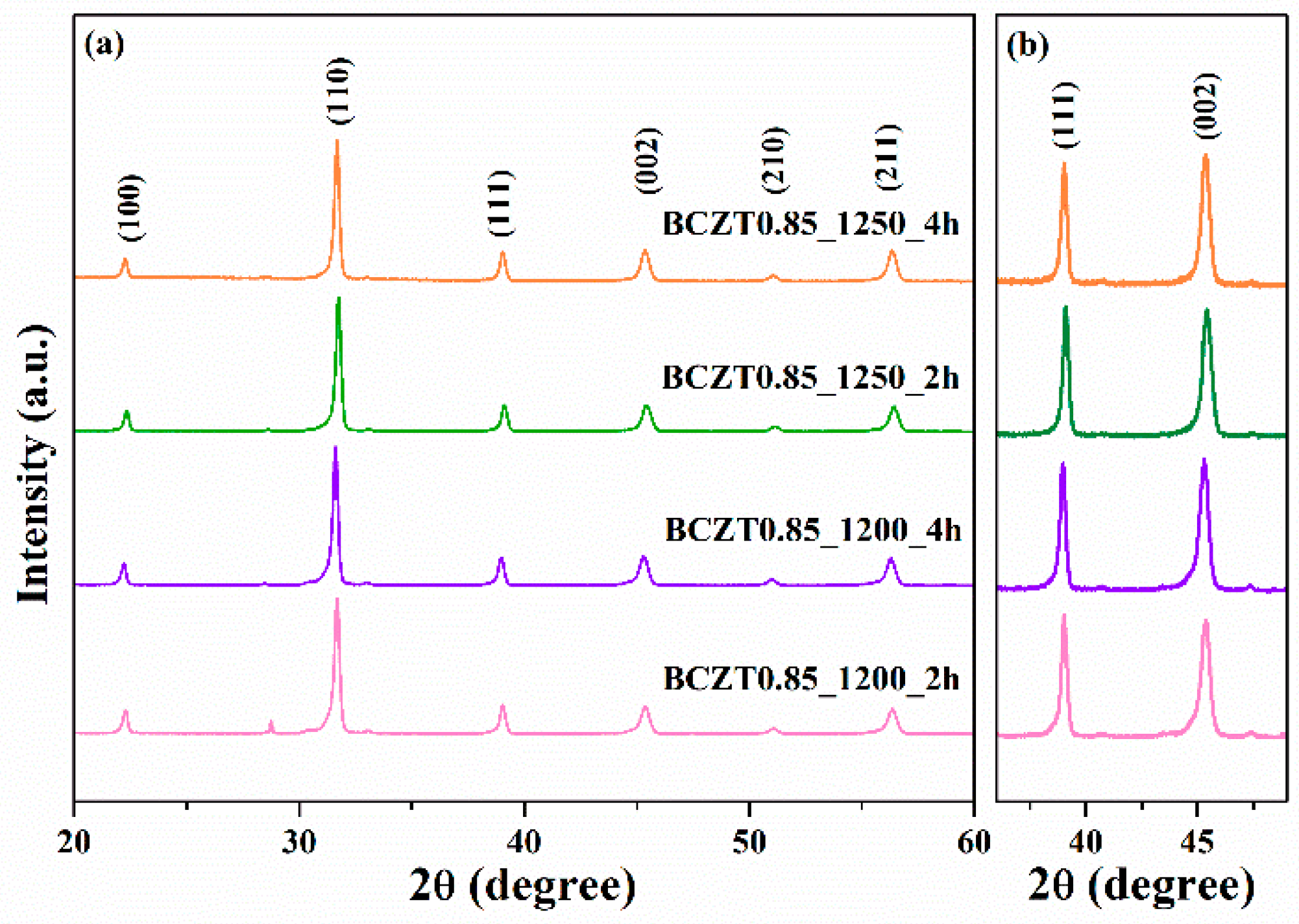
Figure 3.
X-ray diffraction patterns of Ba0.9Ca0.1Zr0.1Ti0.9O3.
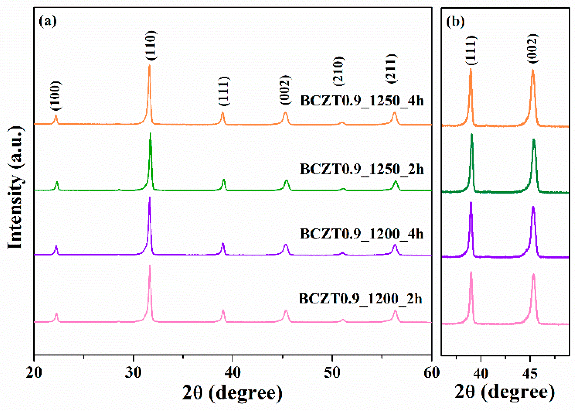
Figure 7.
Dielectric constant(εr) and dielectric loss (tanδ) of Ba0.85Ca0.15Zr0.1Ti0.9O3 ceramics as a function of frequency at room temperature.
Figure 7.
Dielectric constant(εr) and dielectric loss (tanδ) of Ba0.85Ca0.15Zr0.1Ti0.9O3 ceramics as a function of frequency at room temperature.
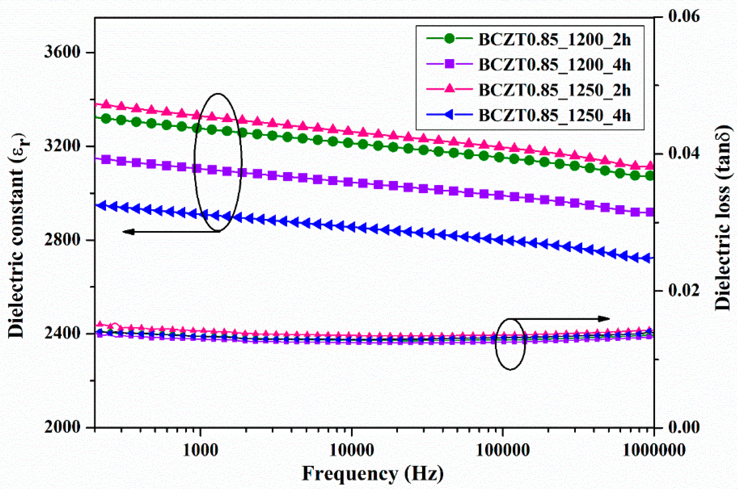
Figure 8.
Dielectric constant(εr) and dielectric loss (tanδ) of Ba0.9Ca0.1Zr0.1Ti0.9O3 ceramics as a function of frequency at room temperature.
Figure 8.
Dielectric constant(εr) and dielectric loss (tanδ) of Ba0.9Ca0.1Zr0.1Ti0.9O3 ceramics as a function of frequency at room temperature.
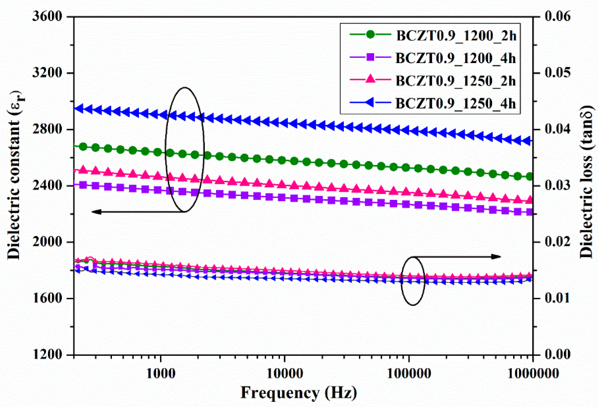
Figure 9.
Temperature dependence of dielectric constant of Ba0.85Ca0.15Zr0.1Ti0.9O3 ceramics.
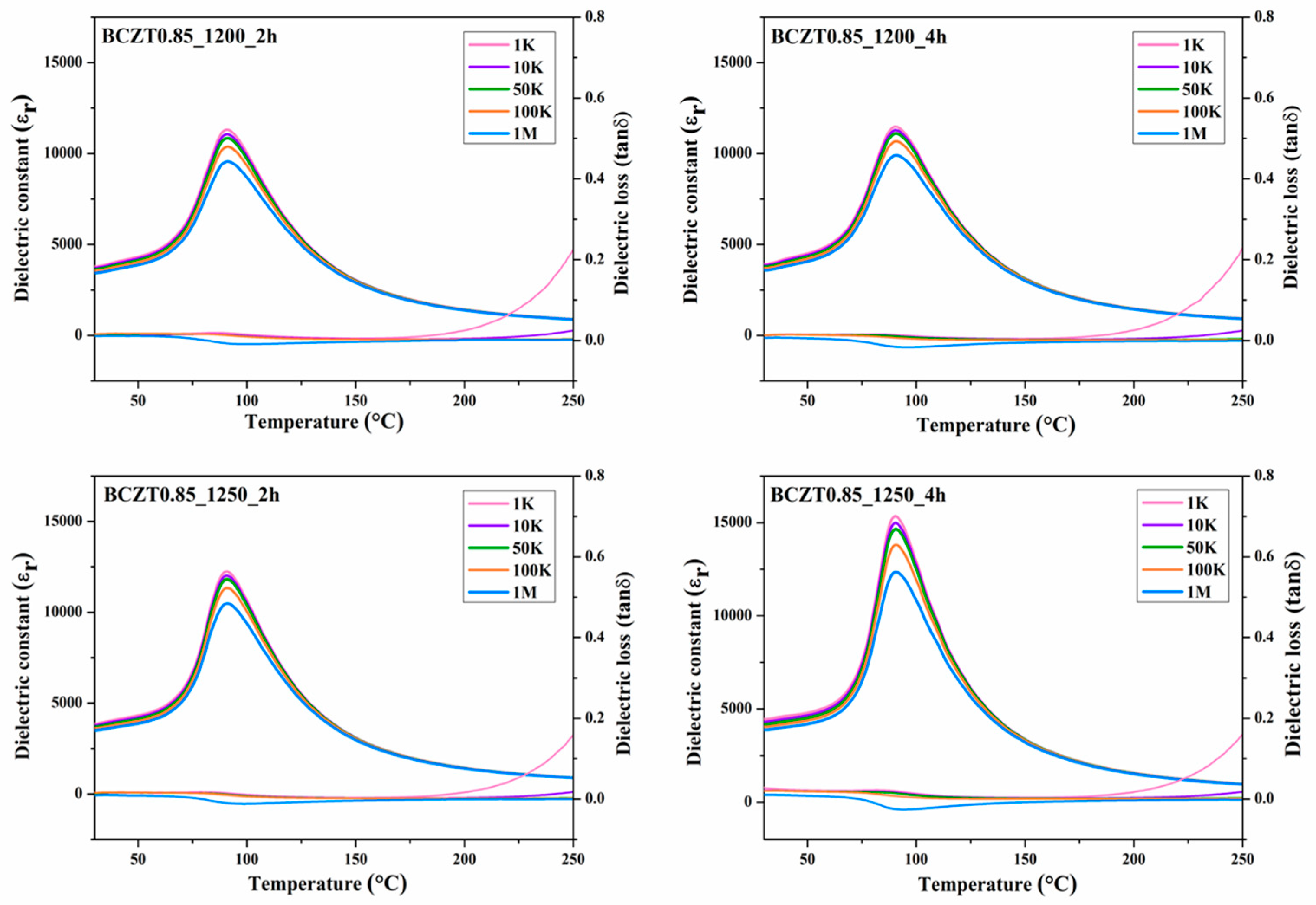
Figure 10.
Temperature dependence of dielectric constant of Ba0.9Ca0.1Zr0.1Ti0.9O3 ceramics.
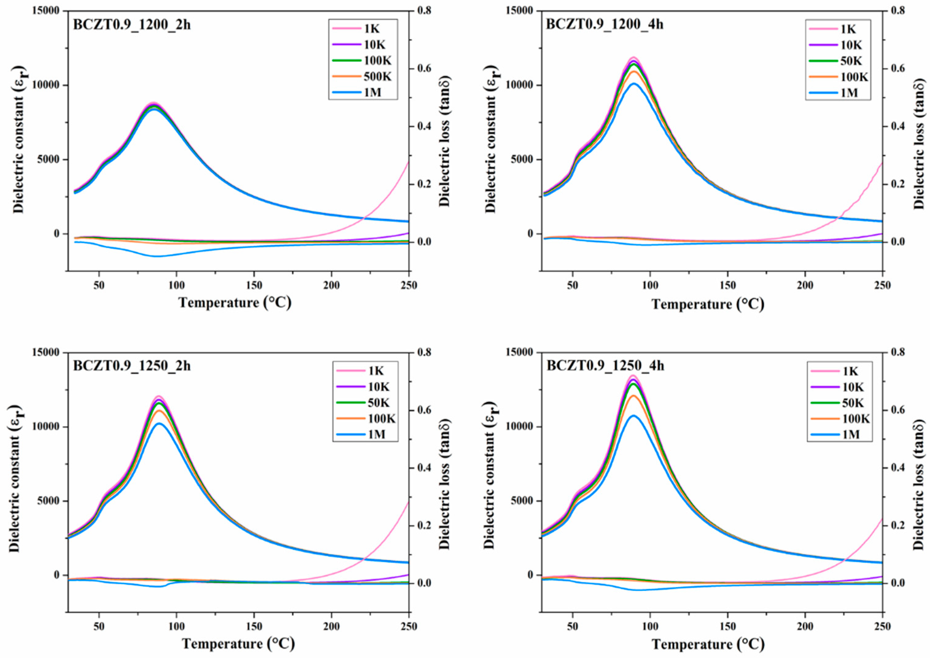
Figure 11.
(a) Ferroelectric hysteresis loops and (b) hysteresis parameter of BCZT.
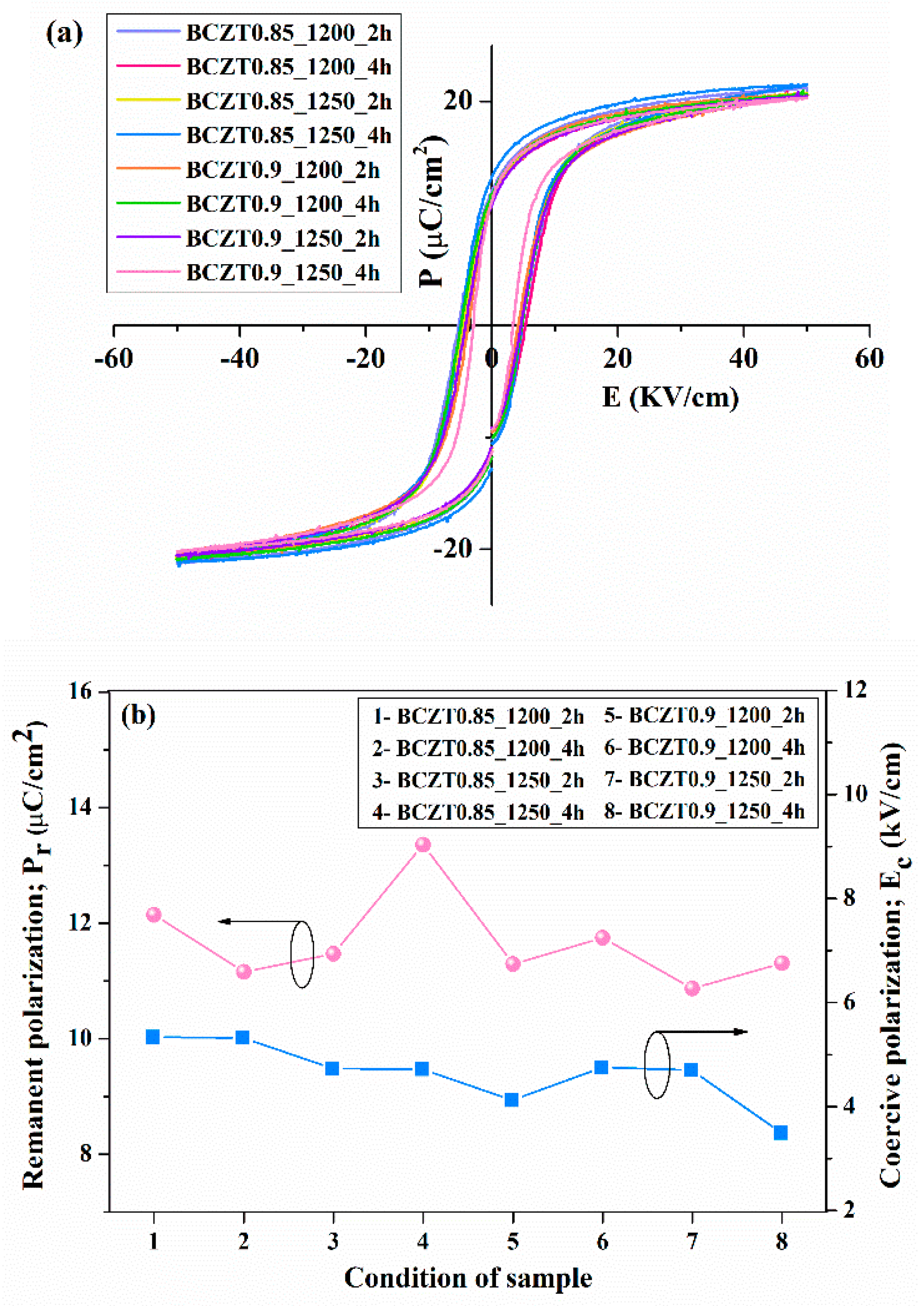
Figure 12.
Dielectric constant(εr) and dielectric loss (tanδ) of Ba0.85Ca0.15Zr0.1Ti0.9O3 films as a function of frequency at room temperature.
Figure 12.
Dielectric constant(εr) and dielectric loss (tanδ) of Ba0.85Ca0.15Zr0.1Ti0.9O3 films as a function of frequency at room temperature.
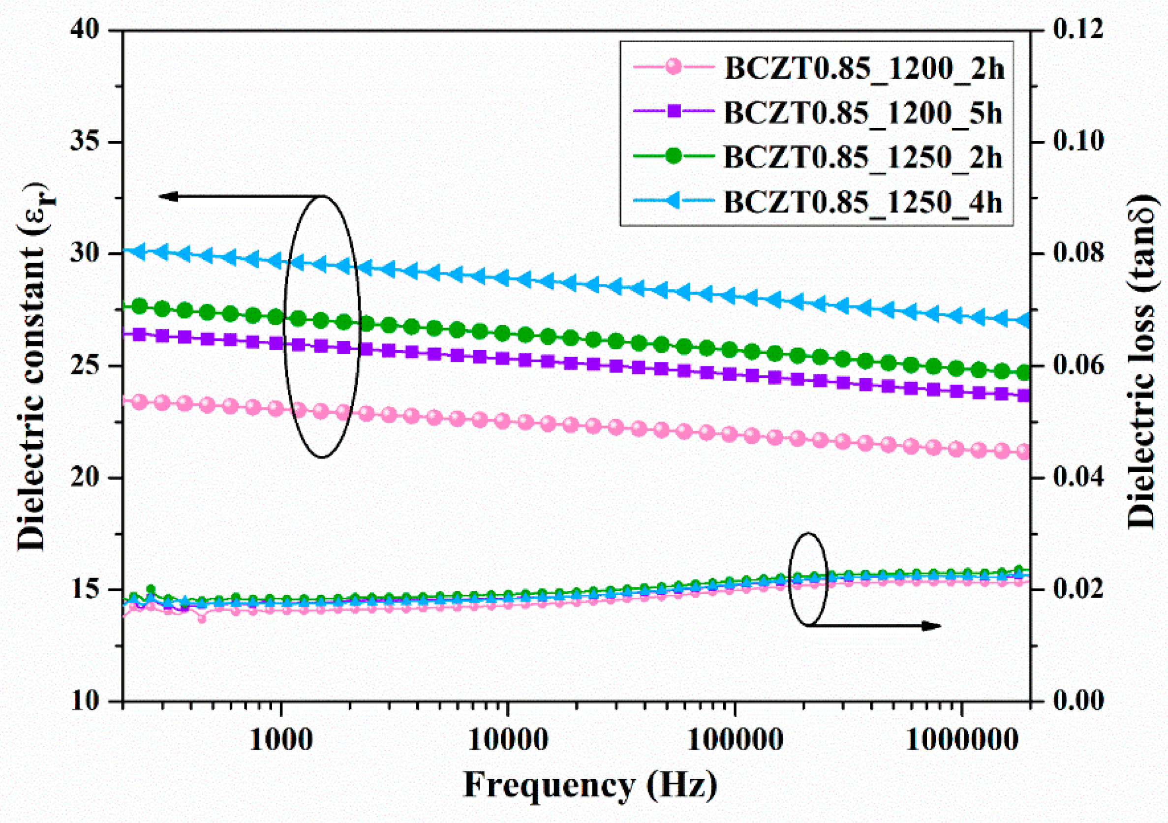
Figure 13.
Dielectric constant(εr) and dielectric loss (tanδ) of Ba0.9Ca0.1Zr0.1Ti0.9O3 films as a function of frequency at room temperature.
Figure 13.
Dielectric constant(εr) and dielectric loss (tanδ) of Ba0.9Ca0.1Zr0.1Ti0.9O3 films as a function of frequency at room temperature.
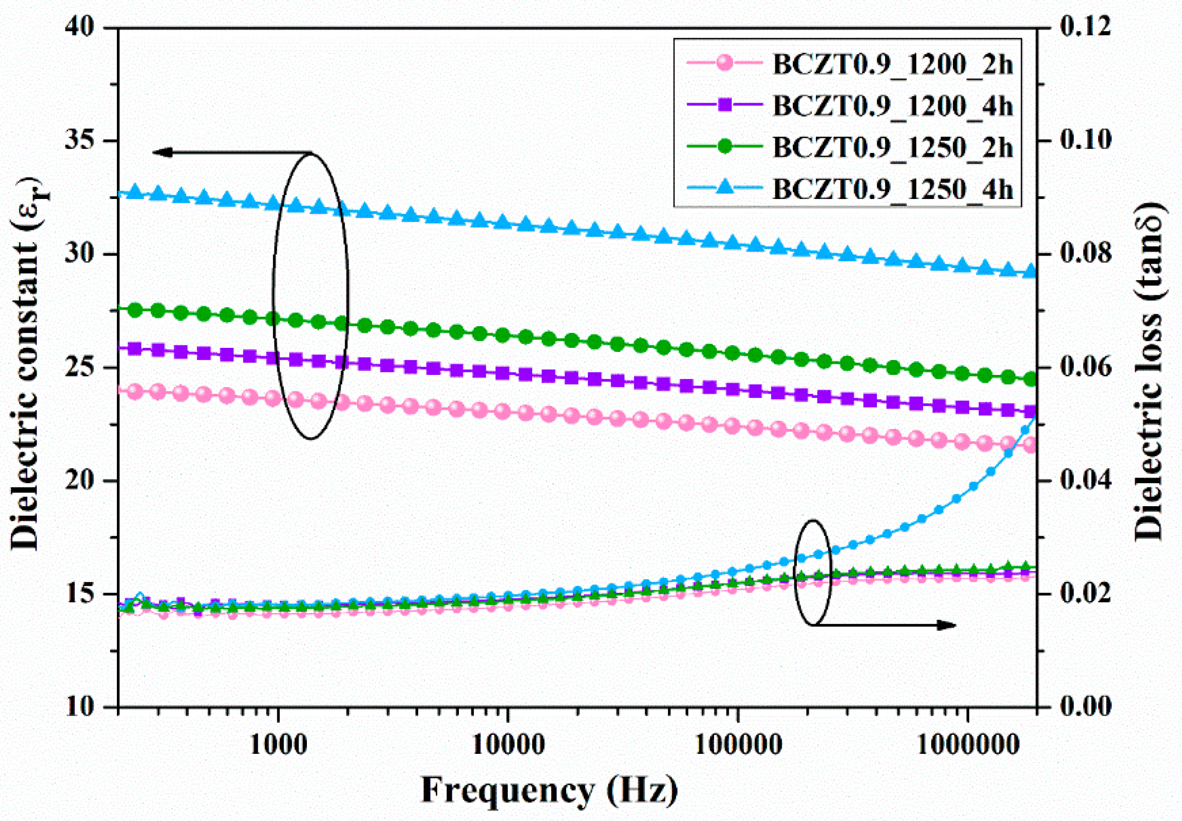
Figure 14.
Temperature dependence of dielectric constant of Ba0.85Ca0.15Zr0.1Ti0.9O3 films.
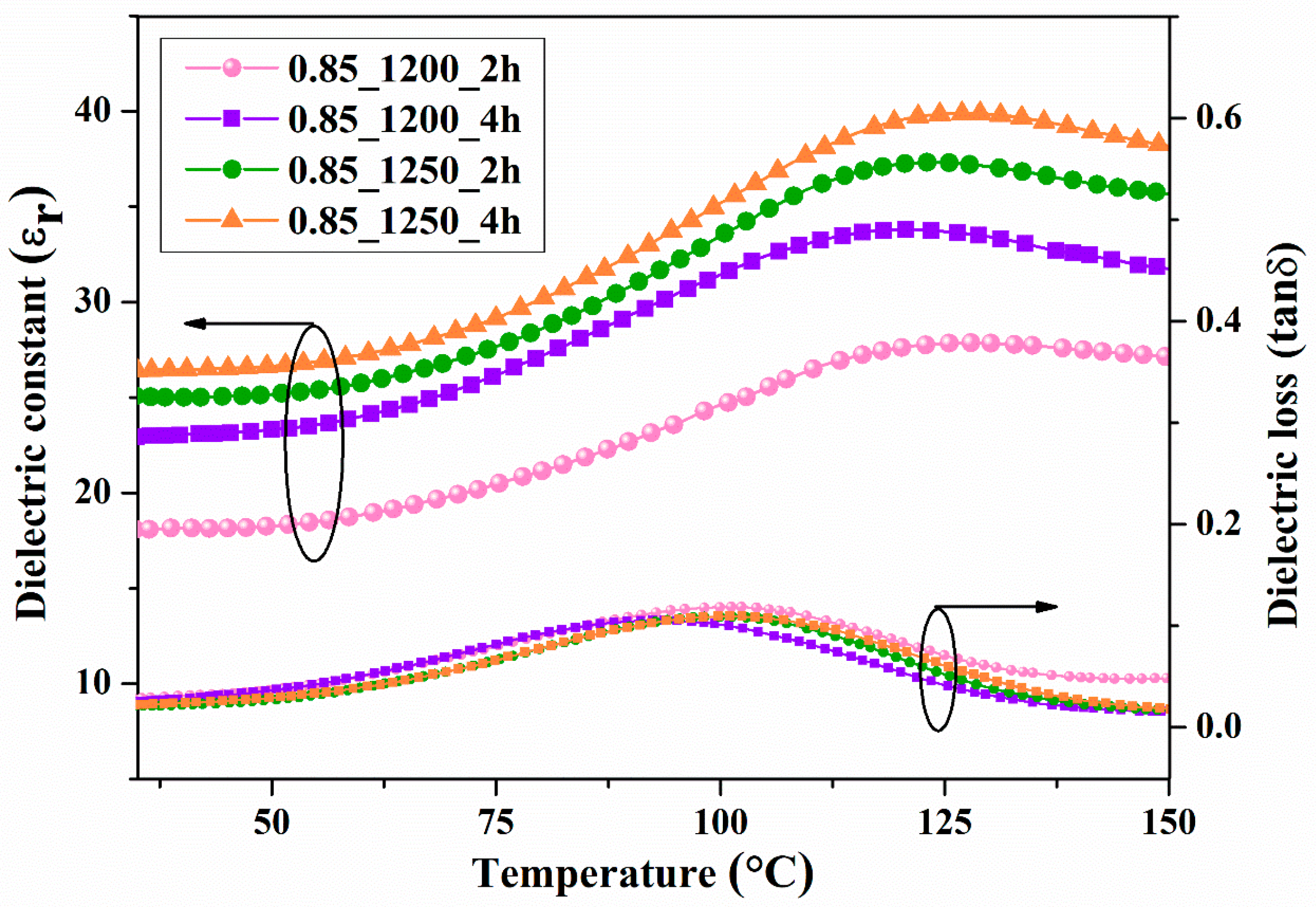
Figure 15.
Temperature dependence of dielectric constant of Ba0.9Ca0.1Zr0.1Ti0.9O3 films.
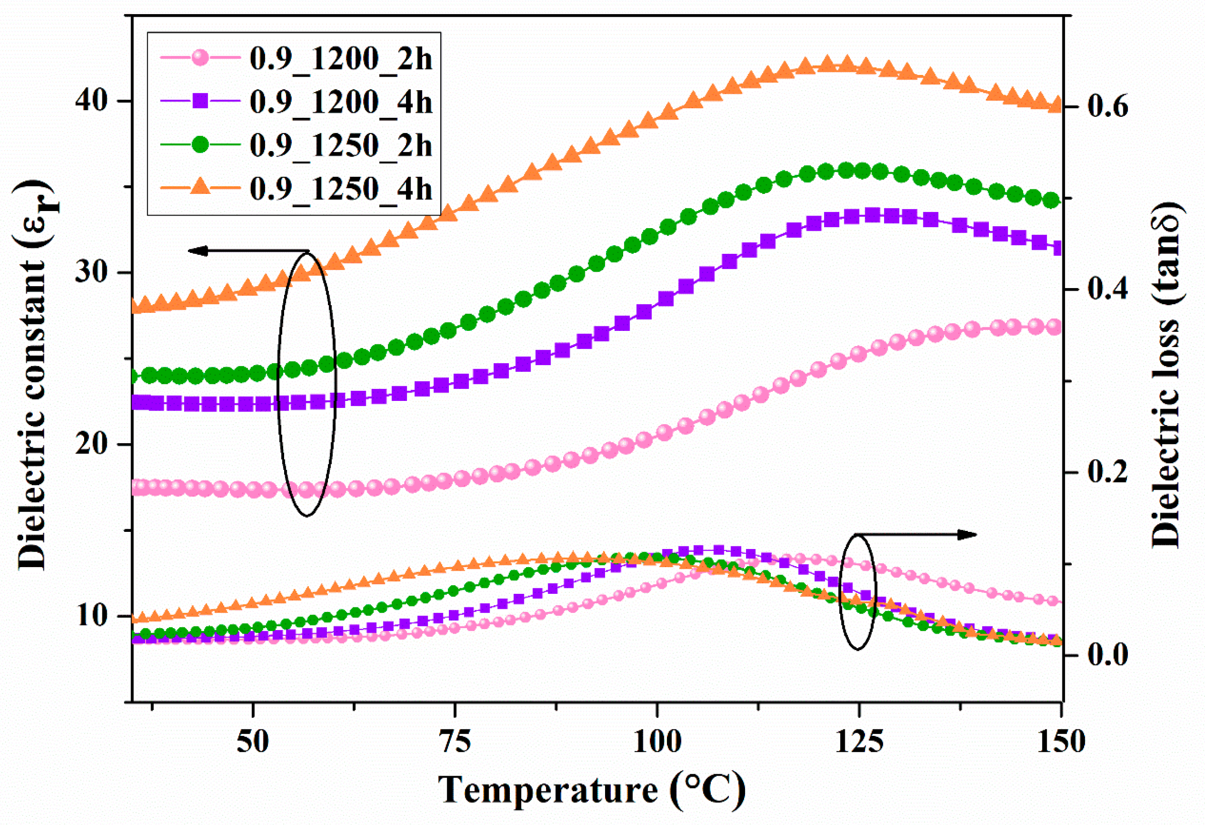
Figure 19.
The CIE color coordinates of an EL device at 25 and 80 °C.
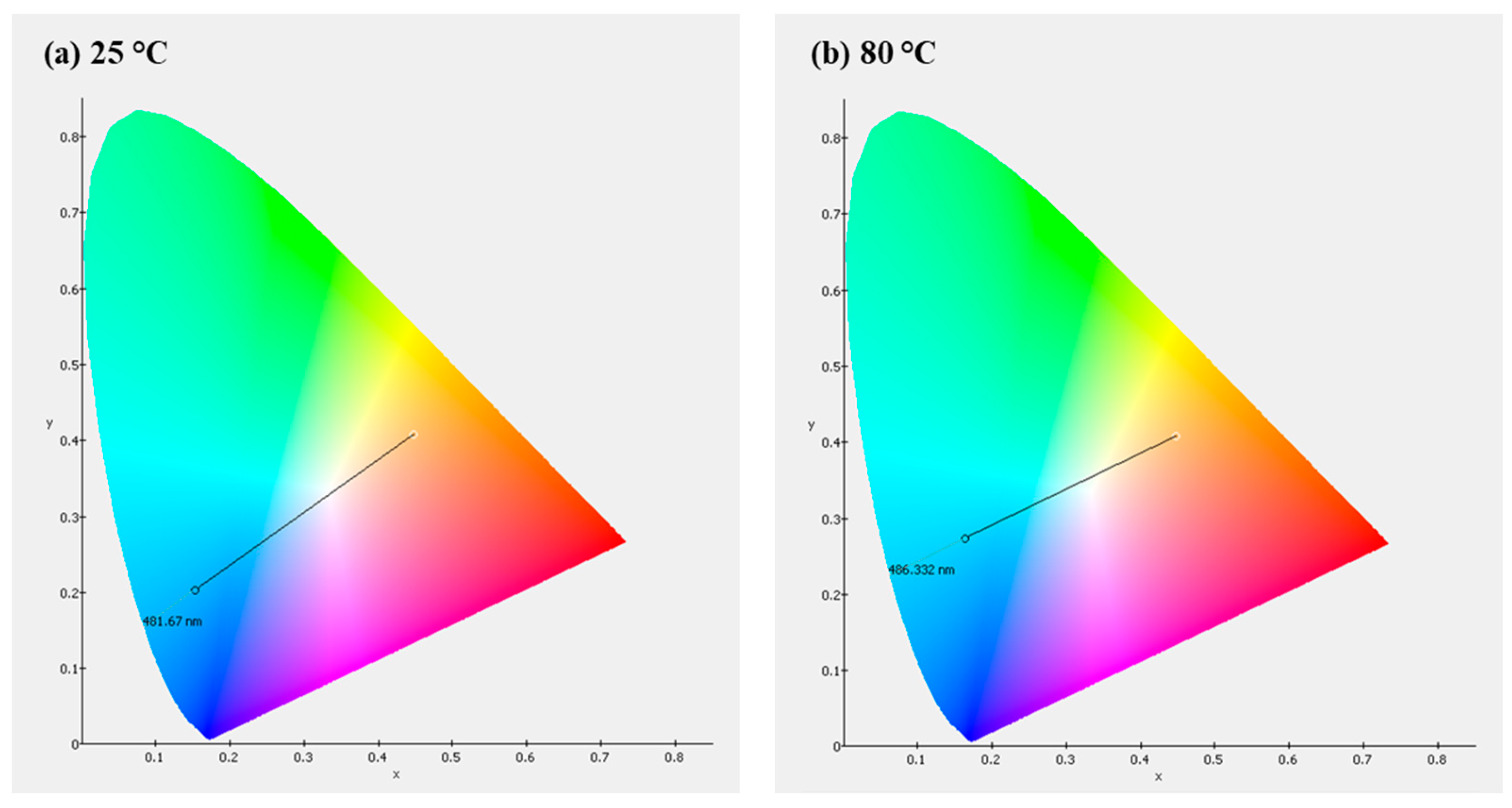
Figure 20.
Photo image of the EL device constructed in this study.
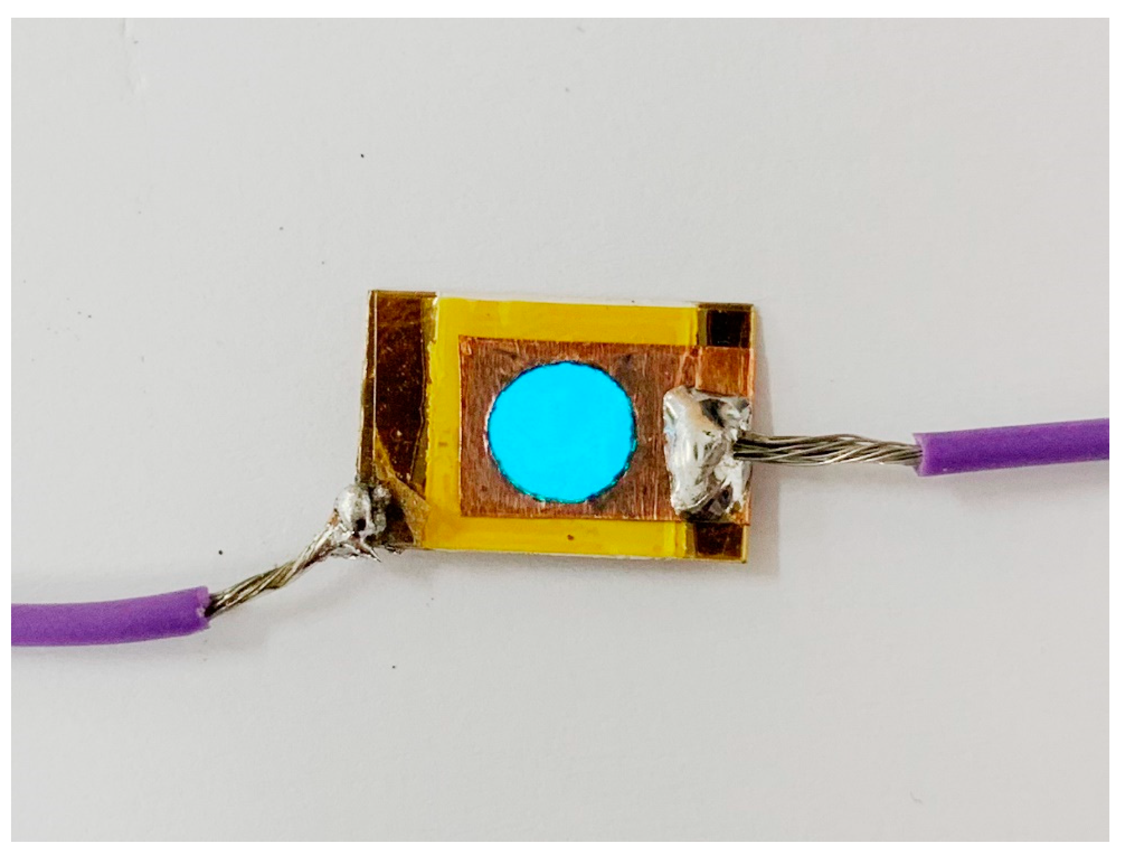

Table 1.
The conditions of BCZT ceramics used in this study.
| Sample | Title 2 | Title 3 |
|---|---|---|
| Temperature (°C) | Dwell time (h) | |
| BCZT0.85_1200_2h | 1200 | 2 |
| BCZT0.85_1200_4h | 1200 | 4 |
| BCZT0.9_1200_2h | 1250 | 2 |
| BCZT0.9_1200_4h | 1250 | 4 |
Disclaimer/Publisher’s Note: The statements, opinions and data contained in all publications are solely those of the individual author(s) and contributor(s) and not of MDPI and/or the editor(s). MDPI and/or the editor(s) disclaim responsibility for any injury to people or property resulting from any ideas, methods, instructions or products referred to in the content. |
© 2024 by the authors. Licensee MDPI, Basel, Switzerland. This article is an open access article distributed under the terms and conditions of the Creative Commons Attribution (CC BY) license (https://creativecommons.org/licenses/by/4.0/).
Copyright: This open access article is published under a Creative Commons CC BY 4.0 license, which permit the free download, distribution, and reuse, provided that the author and preprint are cited in any reuse.


