
Submitted:
29 January 2026
Posted:
29 January 2026
You are already at the latest version
Abstract
Bidirectional Interleaved Converters (BICs) are widely used in Battery Energy Storage Systems (BESS) due to their modular structure, high efficiency, and reduced current ripple. However, under partial-load operation, conventional control strategies with fixed or purely current-based phase shedding repeatedly activate the same converter branches, resulting in increased switching losses, thermal imbalance, and uneven aging of power semiconductors. This paper proposes a temperature-adaptive control strategy for BICs aimed at improving light-load efficiency while actively balancing thermal stress between converter branches. The approach combines a current-adaptive phase-shedding algorithm with a temperature-based branch rotation mechanism, where real-time transistor junction temperature is used as the primary decision variable for branch activation and deactivation. An electro-thermal real-time simulation model of a two-branch BIC is developed using the Controller Hardware-in-the-Loop (CHIL) methodology in the Typhoon HIL environment. The proposed control strategy is validated through real-time CHIL experiments in both boost and buck operating modes under representative battery load profiles. The results demonstrate a reduction in average and peak transistor junction temperatures, improved thermal distribution between converter branches, and more uniform branch utilization, while preserving stable current regulation and power flow. The presented method represents a practical extension of conventional phase-shedding techniques and provides an implementation solution for improving efficiency and reliability of BICs in BESS applications.
Keywords:
bidirectional interleaved converter
; battery energy storage system
; phase shedding
; temperature-adaptive control
; electro-thermal real-time simulation
; CHIL
; Typhoon HIL
; buck and boost operating modes
; transistor junction temperature
1. Introduction
The increasing integration of Renewable Energy Sources (RES), alongside the electrification of transport and industry, has placed Battery Energy Storage Systems (BESS) at the center of modern power system planning. Utility-scale lithium-ion BESS, in particular, offer rapid response, modularity, and bidirectional power flow capabilities, making them a key technology for grid flexibility, frequency regulation, and peak shaving [1].
Reliable projections of storage system costs are essential for long-term energy modeling and investment planning. Recent studies, including the 2023 analysis by the National Renewable Energy Laboratory (NREL), provide scenario-based forecasts of BESS capital cost evolution through 2050 [2]. Figure 1 illustrates normalized cost projections for 4-hour lithium-ion battery systems under low, mid, and high scenarios, with all values referenced to the base year 2022.
The projected cost reductions across low, mid, and high scenarios emphasize the growing role of battery storage in future grid planning and investment modeling. As costs decline, BESS are expected to contribute increasingly to system flexibility, reducing reliance on conventional balancing methods and underscoring the importance of accurate BESS modeling. This trend is exemplified by the European Connected Stationary Battery Energy Storage (USBSE) project, which focuses on modular storage systems combined with aggregator software to reduce building electricity costs and enable participation in grid services, thereby enhancing overall system stability [3]. Figure 2 provides a block diagram of a networked stationary BESS, depicting its main components.
A BESS consists of the battery on the DC side, the grid on the AC side, and a power converter that interfaces these two networks. The hierarchical structure shown in the diagram corresponds to a networked BESS, where a supervisory system coordinates individual units according to distribution requirements, while dedicated control systems are implemented for the battery and the converter. As the core element, the power converter enables bidirectional energy transfer between different frequency domains and therefore requires a bidirectional topology. Owing to this central role, various classification approaches for bidirectional converter topologies have been reported in the literature. For instance, the classification in [4] is based on a few fundamental categories, while [5] presents an application-oriented scheme, using the low-voltage battery as the primary criterion. In this study, a simplified topology map is developed, presenting representative examples from each group, as shown in Figure 3. The converter topology used in this work is highlighted with green. It is important to emphasize that this map has been developed specifically for single-port systems, in contrast to multi-port systems which are predominantly used in RES applications—most notably in photovoltaic systems, which are mostly three-port systems [6].
The topology map in Figure 3 presents the fundamental bidirectional converter configurations, primarily categorized into single-stage and multi-stage categories, each of which can be implemented with or without galvanic isolation. As highlighted here, the multi-stage conversion without galvanic isolation is realized through a cascaded connection of a DC-DC and a DC-AC voltage converters. A similar topology has been implemented in the above mentioned USBSE project for the development of an bidirectional converter [3]. This implementation employs an interleaved DC–DC converter with a three-branch (three-leg) structure, cascaded with a three-phase DC–AC converter, as described in [9]. The schematic of this configuration is shown in Figure 4. The USBSE project served as a practical foundation and key motivation for this research.
In Figure 4, the number of branches (legs) in the DC–AC stage was selected to match the standard three-phase AC grid, utilizing a conventional full-bridge three-phase topology (Stage 2, Figure 4). From a design perspective, the number of branches in the interleaved DC–DC converter (Stage 1, Figure 4) was intentionally aligned with the three-phase DC–AC stage. This design choice allows, in practical implementations, the use of a unified PCB layout for both stages, thereby simplifying system integration and reducing layout-related complexity. This study focuses on the control of the Stage 1 converter (BIC), which represents the first stage of the overall power conversion system.
1.1. Efficiency-Oriented and Thermal Control of Interleaved Converters: State-of-the-Art Review
In the referenced USBSE project [3], the impact of the number of branches on overall converter efficiency was not taken into account during the branch number selection process. Additionally, all interleaved branches were designed for continuous operation, meaning all branches remained active at all times. This raises the question of efficiency under light-load conditions—for example, when the converter operates at one-third of its rated power (e.g., ), where even a single leg of the interleaved converter could meet the load demand. A similar issue was addressed by the authors in [11], who demonstrated that the efficiency of interleaved converters under light-load conditions can be significantly improved by applying a so-called phase-shedding strategy, in which selected converter branches are deactivated during periods of low power demand. In their implementation, the number of active branches was reduced from six to four, resulting in a noticeable decrease in switching losses.
In earlier studies, various methodologies for adjusting the number of active branches in interleaved converters have been investigated to improve performance under light-load conditions. One such approach employs a numerically derived mapping table alongside a dedicated configuration selector, enabling seamless transitions between operational states by identifying optimal switching points based on instantaneous load demands [12]. This form of logic simplifies the control structure while ensuring adaptability across a broad range of operating scenarios.
Another study introduced a digital control solution designed for a three-phase buck converter topology [13]. The proposed system modulated timing parameters to support rapid and smooth adaptation of active branches. Although practical validation was conducted on a converter, the algorithm’s selection mechanism was not the central focus, leaving the selection logic only superficially addressed.
In a separate study [14], dynamic adjustment of the number of active branches was investigated as a method for reducing energy losses under light-load conditions. Two experimental setups, each rated at and configured with four and sixteen branches respectively, were tested and confirmed the viability of this approach. However, the control strategy was not fully developed, as the study primarily focused on measuring the overall loss reduction.
A modular EV charging system was also analyzed in previous studies, featuring three converters, each composed of six interleaved branches [15]. The aim was to dynamically adjust the number of active branches based on the charging requirements, with the goal of improving efficiency and reducing output current ripple. This was achieved by optimizing the control duty ratio; however, the high overall system complexity and the need for coordination across all interleaved branches posed a significant practical challenge.
Research on photovoltaic power converters has also explored dynamic branch adaptation [16]. In this example, a two-branch converter employed a gradual control ramp to reduce transient effects such as current overshoot during branch deactivation. This approach enabled smoother transitions and improved converter reliability.
Other studies have examined simpler three-branch buck topologies, where efficiency improvements under light-load conditions were achieved by reducing the number of active branches [17]. In parallel, current-sharing techniques have been implemented in low-voltage converters operating at high switching frequencies, up to [18].
From the reviewed literature [12,13,14,15,16,17,18], it is evident that load-responsive control of interleaved branches has been widely investigated. Most implementations rely on static logic, often using Look-Up Table (LUT) or LUT-based control schemes triggered by real-time current measurements—typically the battery current in energy storage systems. These approaches commonly reuse the same subset of branches during partial-load operation due to their simplicity. However, such strategies inherently lead to thermal imbalance and uneven component aging, as certain branches are activated more frequently than others, resulting in reduced system reliability over time.
An advanced hybrid approach is presented in [19], where a modular dual active bridge converter integrates both phase-shedding and interleaving techniques. The control system dynamically adjusts the number of active branches and ensures current balancing across modules. This method has shown particular advantages in high-power fast charging applications, providing improved loss reduction and current symmetry through coordinated allocation of modular branches.
A predictive digital control strategy tailored for interleaved multi-branch converters is presented in [20]. Although primarily focused on dynamic current regulation, the architecture also supports integration with phase-shedding control through its cycle-accurate prediction of inductor behavior. This enables smoother transitions between branch configurations and enhances overall system responsiveness.
More recent publications, such as [21,22], have addressed this issue by introducing concepts like active branch cycling or ‘rotation,’ in which switching stress is periodically redistributed across all available branches. This approach extends the operational lifespan of power semiconductors by balancing the cumulative thermal load over time. The concept of rotational phase-shedding is further refined in [21], where the authors propose an efficiency-aware control strategy for EV fast DC chargers based on interleaved converter topologies. The core innovation lies in the periodic reassignment of active branches according to load demand, ensuring thermal uniformity across switching devices while maintaining high efficiency even under light-load conditions.
Based upon [21,22], authors in [23] propose a seamless rotational phase-shedding control algorithm specifically designed to prevent interleaving distortion and current ripple during phase transitions. The method maintains continuous balance between electrical and thermal loading by applying optimized switching sequences. The strategy was experimentally validated on a three-phase synchronous boost converter, demonstrating clear advantages over static or non-rotating phase-shedding approaches.
Lastly, a comprehensive review in [24] not only summarizes phase-shedding techniques but also highlights current branch-rotation strategies aimed at balancing thermal and switching stress across active phases. The described methods include fixed-order round-robin rotation, alternating phase activation, counter-based usage tracking, and sliding-mode-based scheduling. These approaches are intended to prevent uneven phase utilization, thereby enhancing system reliability and extending the operational lifespan of converter components.
However, none of the surveyed state-of-the-art rotation strategies incorporate device temperature as a direct decision-making parameter for branch activation or deactivation. In contrast, the approach developed in this study introduces a thermal feedback loop into the control logic, using real-time measured device temperature as the primary criterion for branch management. This temperature-aware methodology promotes a more uniform thermal distribution among switching devices, which is beneficial for long-term reliability, while indirectly supporting efficiency improvement under partial-load operation. While full implementation of the temperature-adaptive control on a physical converter prototype is planned for future work and is ongoing at the time of writing, the present study focuses on validating the underlying control concept using the Controller Hardware-In-the-Loop (CHIL) methodology, as a foundation for more advanced thermal management strategies.
In this study, the proposed control strategy is developed as an extension of the current-adaptive phase-shedding approach previously introduced in [25], which was primarily aimed at improving converter efficiency under partial-load operation. The current-adaptive algorithm represents a necessary prerequisite within the adopted hierarchical control structure, as it reduces the number of active BIC branches and establishes an efficiency-oriented operating framework. Building upon this framework, the present work introduces a temperature-adaptive branch rotation mechanism, which dynamically redistributes thermal stress among the available branches based on real-time transistor junction temperature. The temperature-adaptive algorithm is therefore conditionally activated only when the current-adaptive phase-shedding mode is engaged. Throughout the manuscript, the role and operating principle of the current-adaptive algorithm are briefly revisited at selected points where required, as this functionality is essential for understanding the motivation and operation of the proposed temperature-adaptive control method.
1.2. Main Contributions and Paper Structure
The primary contribution of this study is the development and validation of a temperature-adaptive control strategy for a BIC used in BESS within an efficiency-oriented control framework. The proposed approach extends a previously established current-adaptive phase-shedding strategy by introducing real-time thermal feedback, implemented and evaluated using a real-time CHIL model, enabling dynamic branch rotation and improved thermal balance under partial-load operation.
The key contributions of this work can be summarized as follows:
- An efficiency-oriented current-adaptive branch control algorithm, previously introduced for partial-load operation, is adopted as a baseline control layer to support efficient branch utilization under partial-load operation.
- A temperature-adaptive extension of the control structure is proposed, enabling dynamic branch rotation based on transistor junction temperature to promote improved thermal balance.
- An electro-thermal real-time simulation model is developed within the Typhoon HIL environment, incorporating power loss evaluation and junction temperature estimation of switching devices.
- The proposed control strategy is validated using real-time CHIL experiments, demonstrating improved thermal distribution and mitigation of temperature peaks across switching devices while maintaining stable operation.
- The complete simulation model and control logic are made publicly available to support reproducibility and further research.
The remainder of the paper is organized as follows. Section 2 introduces the CHIL methodology for control validation. Section 3 presents the electro-thermal modeling of the BIC, including real-time loss and junction temperature estimation. Section 4 describes the control strategy, where temperature-adaptive branch rotation is implemented within an efficiency-oriented current-adaptive framework. Section 5 presents CHIL-based experimental results for both boost and buck operating modes. Section 6 discusses the results with emphasis on thermal behavior under efficiency-oriented operation, while Section 7 concludes the paper and outlines future work.
2. CHIL-Based Testing Methodology
The research methodology employed in this study is the CHIL approach, in which the converter control system is developed, deployed on a real microcontroller, and tested in real time using Typhoon HIL 402 hardware [26]. As this platform represents the primary tool used throughout the study, it is introduced first to keep the rest of the paper easier to follow.
Today, there are several ways to develop a power electronic converter system. Academic researchers usually start with offline computer simulations, while companies in the industry often begin straight with building a physical prototype [27]. Hardware-in-the-Loop (HIL) systems were created to connect these two approaches, combining realistic simulations with reliable results, while avoiding the high cost of building real hardware from the start. The main state-of-the-art methodologies used for power converter development are illustrated in Figure 5.
Figure 5 summarizes development methodologies commonly used in power converter design. Virtual HIL (VHIL) represents a fully simulation-based approach and includes Model-in-the-Loop (MIL), where power and control are integrated within a single model, and Software-in-the-Loop (SIL), where the two domains are modeled separately. In contrast, Power HIL (PHIL) incorporates physical hardware, with the HIL approach using a real microcontroller for control execution while the power stage is emulated via external power amplifiers. The Prototype stage represents a fully functional physical converter.
Bridging the gap between pure simulation and full hardware implementation, the CHIL methodology combines the advantages of both approaches. Here, the converter power stage is simulated in real time using Typhoon HIL software, while the control algorithm is executed on a physical microcontroller, enabling realistic real-time validation of control strategies. The hardware controller interfaces with the simulated power stage through the Typhoon HIL 402 platform (Figure 6a) as with a physical system. In this work, the control algorithm is implemented on the internal 32-bit ARM Cortex-A9 microcontroller, which satisfies the performance requirements and enables full integration of the control system on the embedded platform.
The Typhoon HIL 402 device is built on a mixed hardware architecture that uses several microcontroller units to manage resources during real-time simulation [27], as shown in Figure 6b, and described below. According to the manufacturer [26], each system component shown in Figure 6b is responsible for specific tasks:
- FPGA Solver: A multi-core FPGA-based processor (Xilinx XC7Z030 Zynq SoC) executes the real-time converter model with a minimum simulation step of
- User Microcontroller: A 32-bit ARM Cortex-A9 running at executes the user control algorithm, with control time steps defined as integer multiples of the base simulation step, typically in the tens to hundreds of microseconds range.
- System Microcontroller: A 32-bit MicroBlaze processor with memory manages low-dynamics components and system-level functions, including virtual instruments, switches, and communication protocols.
In the CHIL-based real-time simulation setup, the electrical domain of the converter, i.e., the power stage, is executed on the FPGA solver, while the signal domain, including the control section, runs on the user microcontroller (internal or external). The DSP interface module (Figure 6a, mark 2) enables connection of any microcontroller with compatible I/O voltage levels and provides both analog and digital interfaces, allowing integration of external measurement instruments such as oscilloscopes. This configuration enables signal monitoring and data acquisition in both the electrical and control domains. In the developed setup, the digital I/O of the user microcontroller is connected through this interface, and the corresponding signal routing is shown in Figure 7.
Future research will certainly include the use of external microcontroller units, such as the Texas Instruments F28379D DSP system (Figure 6a, mark 3) [28], especially for ongoing control development implementation using PHIL methodology. The overall development process presented in this paper, based on the CHIL methodology within the Typhoon HIL environment, is summarized by the flowchart shown in Figure 8. The process begins with the development of a complete converter model in the Typhoon HIL Schematic Editor, incorporating both the power stage and the control sections. The schematic representations of the developed Typhoon HIL subsystems are provided in Supplementary files on public repository [29]. Once the accuracy of the model is verified, it is deployed to the appropriate microcontroller systems within the Typhoon HIL hardware—the power stage is implemented on the FPGA, while the control section is executed on the internal user microcontroller.
The term ‘experimental setup’ does not solely refer to the converter and its components designed in Schematic Editor, but also includes the user SCADA (HMI) interface, which enables monitoring of all control parameters, waveform recording, and system supervision. Therefore, after implementing the control algorithms and the power stage model, it is also necessary to develop the user interface. To get better insight, a screenshot of the developed SCADA interface within the Typhoon HIL SCADA environment is taken and shown in Figure 9.
2.1. Typhoon HIL 402 Hardware Configuration
A key aspect of real-time HIL modeling is the correct configuration of the Typhoon HIL 402 hardware to ensure stable operation of the microcontrollers used in the control system. Table 1 summarizes the key settings configured in the Typhoon HIL environment and deployed to the hardware via the Typhoon HIL Schematic Editor. The Typhoon HIL 402 system offers six hardware configurations that define FPGA memory allocation and modeling capabilities. For this study, Configuration 4 was selected, as it uniquely supports real-time thermal modeling of up to four power components, enabling the implementation of a two-branch BIC with a battery. This capability is essential for converter loss simulation and transistor junction temperature estimation required for the proposed temperature-adaptive control approach.
In such configuration, resources can be allocated across two cores of the FPGA solver, enabling faster simulation and faster memory optimization. The execution interval (step size) for the ARM Cortex-A9 microcontroller commands was determined experimentally using a trial-and-error approach, optimizing parameters for maximum utilization of available resources. Three different execution intervals (), which are multiples of the fundamental simulation step, were implemented on the user microcontroller to enhance core utilization efficiency, as shown in Table 1.
After reviewing the key features of the Typhoon HIL 402 hardware and other critical aspects of the experimental setup, the subsequent section presents the selected two-branch BIC modeling approach in more detail.
3. Modeling of the Bidirectional Two-Branch Interleaved Converter
A two-branch BIC was selected as the minimal configuration required to validate the proposed control algorithm, considering the real-time simulation limits of the Typhoon HIL 402 platform. Since the applied control strategies explicitly account for thermal behavior, a corresponding thermal simulation model was developed starting from an open-loop converter configuration (Figure 10). A concise overview of the model development is therefore provided, focusing on the CHIL methodology and the key parameters underlying the enhanced control approach. The converter model was implemented in the Typhoon HIL environment and executed in real time on the Typhoon HIL 402 platform with the embedded control algorithm.
As the model is based on a converter design currently under development, component selection is briefly discussed, allowing the presented framework to serve as a reference for future PHIL validation and direct comparison with physical hardware. Namely, in a real single-phase BESS with a rated power of , the DC-link voltage must be maintained at approximately to ensure that the rectifier, when operating in inverter mode, can provide an output voltage of [30,31]. Battery voltage levels in single-phase BESS's typically range between and [30,32]. For safety reasons, as well as cost-effectiveness, the proposed BSE system is chosen to be scaled down. The battery pack, as the starting point for the design, is selected for a nominal voltage of , while the DC-link voltage is set at . This ensures that the system’s voltage levels correspond to those in a real system, scaled by a factor of approximately .
3.1. Model Parameter Selection
The selected basic parameters of the converter and BESS are given in Table 2. These parameters are based on the concept of developing a scaled model of a real BIC (based on [3]), intended for application in a BESS for residential use as one of the cascaded converters in the system.
Since the BIC is designed for scaled BESS, it is important to also consider the battery pack parameters to clarify the rationale behind the selected values. These parameters are provided in Table 3. In this setup, the battery pack consists of series-connected cells, forming a single module, with such modules connected in parallel to increase capacity. This configuration is denoted as 7S3P.
Finally, it is necessary to present the selected electronic components of the actual system on which this model is based, to clarify the rationale behind their selection. The component selection process and calculations will not be included here, as they are not essential to the workflow of this study. However, they will be detailed in future work during the development of the physical prototype, which is planned based on the research findings presented in this study. The key selected components of the system are listed in Table 4.
3.2. Typhoon HIL Real-Time Simulation Model
Figure 10 shows the initial version of the power section of the two branch BIC model, developed in Typhoon HIL in an open-loop configuration. This simplified model was created to provide insight into the simulation environment, as the complete Typhoon HIL model is too extensive to be presented here. The full schematic of the final model will be given in Supplementary materials in a public repository [29].
Analyzing the converter in an open-loop configuration provides insight into its fundamental behavior, which is clearly illustrated by the simulation results for the boost mode shown in Figure 11.
The simulation model from Figure 10 is compiled and implemented into a real MCU via Typhoon HIL Schematic Editor software. Here, simulation model uses an internal PWM modulator with a switching frequency , a duty cycle , and a signal phase shift of between the branches. Figure 11a confirms the input-output voltage ratio corresponds to a duty cycle, but it does not indicate the power flow direction. To clarify this, Figure 11b presents inductor currents , and battery current , along with transistor control signals and .The inductor currents are positive, which aligns with the defined reference current flow direction of the system (boost mode). The above configuration was intentionally chosen to highlight the advantages of using a BIC's, where, with an optimal selection of branches and optimal phase shift, the battery current remains practically ripple-free (smoothed) which is visible in Figure 11b. Namely, battery current ripple has a direct impact on battery lifespan, as demonstrated in [33]. For this reason, some manufacturers specify a maximum allowable current ripple during charging and discharging of lithium-ion and lead-acid batteries within a to range [34], which was considered in the design of the proposed converter system. To provide a clear reference for the subsequent development of the regulated simulation model, the BESS converter together with all essential components is presented as a block diagram in Figure 12, depicting a two-branch BIC consisting of Branch 1 and Branch 2.
This diagram forms the basis for the controlled model with integrated control blocks, whose detailed implementation within the Typhoon HIL simulation environment is provided in the Supplementary Materials [29]. The battery is located on the left side of the converter, while the DC link is positioned on the right side. Each branch is equipped with an associated inductance, whereas both the battery and the DC link are interfaced through capacitive voltage filters to ensure stable operation. Owing to the bidirectional nature of the system, the source and load roles interchange depending on the operating mode, i.e., boost or buck operation. Consequently, both terminals are consistently represented by battery symbols throughout this study, while the terms battery side and DC-link side are used for terminological clarity.
The control architecture of the converter is illustrated through a hierarchical structure in which the individual functional blocks are coordinated by a higher-level Power flow control system. Here, the variables and denote the desired inductor currents for the boost mode set by the user, while and denote the desired inductor currents for the buck mode, as defined by the user and the battery charging control algorithm. Within the Typhoon HIL software environment, in addition to the automatic algorithm, the control strategy is also implemented in an optional simplified form that allows manual selection of the operating mode. Such configuration enables clear differentiation between boost and buck operation during testing and validation, while preserving full control over the direction of power flow. The transition between operating modes is managed by the Power flow control block in coordination with the Mode switch logic block.
The measurement system incorporates four current sensors to monitor the individual branch currents ( and ), the battery current (), and the DC-link current (). In addition, two voltage sensors are used to measure the battery voltage () and the DC-link voltage (). During boost operation, the individual branch currents ( and ) and the DC-link voltage () represent the critical control variables, whereas in buck operation, the branch currents ( and ) and the battery voltage () are the primary monitored quantities.
The active switches (MOSFETs in real converter) are defined according to the selected operating mode. In buck operation, the lower MOSFETs ( and ) are engaged, whereas in boost operation, the upper MOSFETs ( and ) are activated. This switching arrangement corresponds to an asynchronous control strategy, whose operating principles and design rationale are discussed in detail in the subsequent section.
In BIC topologies, the choice of operating mode represents a fundamental design decision and can be realized using either synchronous or asynchronous control [35]. In asynchronous operation, a single MOSFET is actively switched while the complementary device conducts through its body diode. In contrast, synchronous operation employs complementary gate driving of both MOSFETs, with the auxiliary switch replacing diode conduction to reduce conduction losses [36].
In this work, asynchronous control is adopted in accordance with the described switching arrangement and overall control architecture. Beyond the switching strategy itself, an additional architectural consideration in BESS converter control is the selection between unified and separate controller structures, which represent two widely adopted control approaches [37]. The asynchronous operating mode is naturally aligned with a separate controller strategy, in which buck and boost operations are treated as independent control subsystems. This separation simplifies mode management, facilitates independent tuning of control loops for each operating mode, and reduces the risk of cross-coupling effects during bidirectional power flow. The relationship between asynchronous control and the charge/discharge regulator characteristics of the battery, based on a separated regulator structure, is illustrated in Figure 13.
The decision to implement asynchronous operation in combination with separate regulator circuits is primarily motivated by the requirement for precise tuning of control loops under distinct operating conditions. From a practical standpoint, this approach also mitigates challenges related to transistor dead time and other implementation issues inherent to synchronous control, which may become critical in real-world applications. A detailed comparative discussion of synchronous versus asynchronous operation, as well as unified versus separate controller structures, is provided in [36].
Dual-loop Control Strategy
Within the Boost mode and Buck mode control blocks (Figure 12), independently configured proportional–integral (PI) controllers are implemented for each operating mode. These controllers are specifically tailored to the distinct dynamic characteristics of boost and buck operation. As the detailed design of the PI control loops is not the primary focus of this study, only the key elements relevant to the proposed control strategy and system behavior are briefly outlined in the following discussion.
For the purposes of this research, a linear proportional–integral (PI) controller is adopted, as it satisfies the digital resource constraints of the Typhoon HIL 402 system. Within the considered operating range, the linear PI controller provides control accuracy and dynamic performance comparable to more advanced nonlinear approaches, such as sliding mode control. At the same time, it offers the advantages of a robust structure and straightforward digital implementation, as reported in [38].
The PI controller enables regulation of current and voltage, and consequently of the transferred power. Voltage-oriented control is particularly suitable for systems with limited load variations or low current ripple, as demonstrated, for example, in [39] for a four-branch boost DC–DC converter. However, in applications requiring accurate current sharing and precise current regulation—especially in multi-branch converter topologies—the industry-standard approach is dual-loop control. Accordingly, this control strategy is adopted in the proposed model, as illustrated in Figure 14 for the boost mode (the same structure applies analogously to the buck mode).
In Figure 14, the outer control loop regulates either the battery voltage or the DC-link voltage, depending on the selected operating mode. The inner control loop comprises two independent current controllers, each assigned to one converter branch. This hierarchical structure enables fast dynamic response through the inner current loops, while the outer voltage loop ensures accurate and stable voltage regulation.
3.3. Electro-Thermal Modeling
Since the primary contributions of this study are focused on temperature-based regulation strategies, the development of an electro-thermal model is essential as a foundation for the Typhoon HIL implementation, which is presented later in this work. Consequently, a concise theoretical overview of the thermal modeling fundamentals is required to establish the basis upon which the simulation framework is constructed.
In power converters, electrical losses are dissipated in the form of heat, leading to a temperature rise in the system components. Temperature represents a critical factor in the assessment of reliability and lifetime of electronic devices, particularly in power converter components such as transistors and integrated circuits, where semiconductor switches constitute the core functional elements [40]. To model the thermal behavior of the system, transistor operation is represented using an equivalent thermal–electrical network. While this analogy is conceptually straightforward, the accurate development of thermal models can become highly complex due to the nonlinear and dynamic nature of heat generation and dissipation in power semiconductor devices [41].
Power semiconductor transistors represent the most temperature-sensitive components in power converters. Junction temperature () has a pronounced impact on their electrical characteristics, conversion efficiency, and operational lifetime. As the junction temperature increases, switching performance deteriorates, power losses rise, and the probability of device failure increases. Furthermore, repetitive temperature variations induced by dynamic loading accelerate device aging through thermo-mechanical stress mechanisms [42]. Additionally, due to manufacturing tolerances, transistors of the same type may not exhibit identical electrical characteristics, which can result in uneven current sharing and temperature imbalance in parallel component/converter configurations. Accurate temperature monitoring is therefore essential to ensure safe and reliable operation. To realistically capture the thermal behavior of the system, the electrical and thermal models must be dynamically coupled.
In power converter design, thermal models are commonly implemented using electrical analogs to represent heat transfer phenomena. While heat conduction is the dominant mechanism within semiconductor devices and packaging, system-level heat dissipation also involves convection and radiation, particularly when heatsinks or active cooling solutions are employed, as illustrated in Figure 15.
Thermal behavior can be represented using several modeling approaches, among which the Foster and Cauer models are the most commonly employed. Both approaches are based on equivalent thermal networks composed of resistances and capacitances, commonly referred to as RC networks [43]. For a single branch of BIC considered in this study, the Cauer thermal model is adopted and illustrated in Figure 16.
In the thermal model shown in Figure 16, the discrete transistors and are modeled individually, with each device requiring a separate thermal model, although both share a common heatsink. An electrically insulating layer is placed between the transistor package and the heatsink to ensure electrical isolation, since the transistor casing is electrically connected to the MOSFET drain. Each thermal interface—namely the transistor junction-to-case (), the insulating layer, and the heatsink—introduces an additional RC stage that must be characterized by appropriate thermal parameters. These parameters are typically provided in the component datasheet; however, in certain cases, they may need to be identified experimentally. As an illustrative example, the STM VNP10N07 MOSFET, which is one of the options planned for integration in the physical prototype, provides sufficient thermal data in its datasheet to enable direct implementation of the corresponding thermal model [44].
The extracted thermal data are subsequently used within the Typhoon HIL environment, which supports both Foster and Cauer thermal modeling approaches, as well as conversion between them when required. Although some semiconductor manufacturers provide predefined SPICE-based thermal models for their devices, such models remain relatively uncommon. In the present case, no predefined thermal model was available, underscoring the need for wider industry adoption of standardized and readily accessible thermal models in order to improve the accuracy, reproducibility, and efficiency of electro-thermal simulations.
Real-Time Thermal Modeling in Typhoon HIL 402
The basic simulation model was developed in the Typhoon HIL environment and is presented in simplified form in Figure 12. This initial electrical model was subsequently extended with an additional thermal layer to capture the temperature-dependent behavior of the converter. A review of the existing literature indicates that the integration of electrical and thermal models for real-time converter simulation remains relatively uncommon, particularly in the context of HIL platforms. Consequently, the proposed modeling approach represents a novel contribution and motivates a brief explanation of the model construction and implementation methodology. Starting from version 2021.3, the Typhoon HIL software introduced native support for thermal modeling of power converter components, a feature that has been maintained in all subsequent releases. These capabilities include configurable heatsink thermal parameters and detailed thermal model setup for power semiconductor devices such as MOSFETs and IGBTs, as illustrated in Figure 17.
Within the Typhoon HIL environment, transistor conduction and switching losses can be estimated using thermal models based on either the Cauer or Foster approach, with the option to incorporate heatsink thermal behavior directly into the simulation. When executed on Typhoon HIL 402 real-time hardware, the combined electro-thermal model enables real-time observation of temperature dynamics, thereby enhancing the fidelity and reliability of thermal behavior prediction.
Figure 17b illustrates the interface for entering the parameters of the Cauer or Foster heatsink thermal model. In practice, heatsink manufacturers most commonly provide only a single steady-state thermal resistance value, typically specified as the case-to-ambient thermal resistance. While sufficient for rough thermal estimation, this information is inadequate for precise implementation of Foster or Cauer thermal networks, which require multiple thermal resistances and capacitances to describe transient thermal behavior. Some manufacturers, such as Wakefield-Vette, additionally provide power dissipation versus thermal resistance characteristics for TO-220 and TO-247 transistor packages [45]. However, even these datasheets generally do not include time-dependent thermal impedance data required for systematic extraction of Foster or Cauer model parameters. As a result, heatsink parameters in electro-thermal simulations must be approximated or empirically tuned, which introduces modeling uncertainty and represents a limitation of the presented simulation framework.
By enabling the Losses Calculation and Temperature Calculation options (Figure 17a), the standard MOSFET model is functionally extended with additional input and output signals (Figure 17b). The T_junctions output provides a real-time estimation of the internal junction temperature of the transistor, while the P_loss and T_cases signals supply thermal feedback from the MOSFET to the associated heatsink model block. This configuration enables comprehensive simulation of the thermal behavior, allowing temperature prediction at both the semiconductor junction and the heatsink level. The model employs user-defined thermal parameters to accurately estimate conduction and switching losses. Unlike simplified approaches in which losses are assumed constant, the proposed modeling framework accounts for their dependence on the estimated junction temperature. All required thermal input parameters—such as thermal resistances and capacitances—are typically obtained from the device datasheet, most commonly provided in the form of a Foster network representation.
In the simulation model, MOSFET conduction losses are calculated based on the voltage drops across both the main switching channel (Vt) and the internal body diode (Vd). These voltage drops depend on both the operating current and the junction temperature. To accurately capture this behavior, a two-dimensional lookup table (2D LUT) is employed, constructed using characteristic data provided in the manufacturer’s datasheet, as illustrated in Figure 18a.
On the other hand, switching losses are estimated based on the energy dissipated during individual switching events, namely the turn-on and turn-off transitions of the MOSFET and its body diode. These losses depend on three primary variables: the operating current, the junction temperature, and the drain-to-source voltage. To capture these dependencies, a three-dimensional lookup table (3D LUT) is implemented, enabling dynamic estimation of switching losses over a wide range of operating conditions, as illustrated by the three-dimensional surface plot in Figure 18b.
Obtaining accurate switching loss data from manufacturer datasheets can be challenging, as such information is frequently incomplete or entirely omitted. In many cases, switching energy loss tables are either not provided or presented in non-standardized formats, limiting their direct applicability for detailed electro-thermal modeling. To mitigate this issue, guidance provided by Typhoon HIL technical support recommends the use of equivalent transistor models with known parameters when the required device-specific data are unavailable. An additional limitation arises from the scarcity of publicly available electro-thermal models defined in XML format, despite this representation offering the highest level of accuracy for device characterization within the Typhoon HIL environment. In the context of this study, the exact transistor type is not critical, as the primary focus lies on the modeling methodology rather than on device-specific behavior.
Accordingly, most simulation parameters are derived from available datasheet information [44]. These limitations highlight that electro-thermal modeling of power semiconductor devices remains an underdeveloped area and warrants further standardization and broader industry support. Only a limited number of manufacturers provide thermal models based on Foster or Cauer network representations, and those that do often rely on proprietary formats or internal standards. Furthermore, variations in measurement methodologies and inconsistencies in datasheet specification formats across manufacturers significantly complicate accurate thermal modeling. As a result, reproducing real-world device behavior based solely on datasheet information remains challenging.
To conclude the thermal modeling section, the complete converter schematic with integrated electro-thermal features is provided in the Supplementary Materials [29]. The incorporation of electro-thermal modeling enables real-time estimation of the temperature of individual converter components, thereby establishing a foundation for advanced control enhancements. In particular, the developed simulation framework supports both a current-adaptive control strategy for managing the number of active branches and a temperature-adaptive control strategy for branch rotation. These control approaches are described and analyzed in more detail in the following section.
4. Temperature-Adaptive Branch Rotation in an Efficiency-Oriented Control Framework
By augmenting the basic simulation model (Figure 10) with the thermal model presented in Section 3, it becomes possible to analyze converter losses and thermal behavior in a temperature-dependent manner. In this extended framework, the generated losses are no longer determined solely by the operating load, i.e., the current, but additionally depend on the junction temperature estimated by the electro-thermal model of the converter. This allows the interaction between electrical loading, loss generation, and thermal response to be evaluated within a unified simulation environment.
Consequently, the simulation framework has been extended to support user-controlled activation and deactivation of individual converter branches. This functionality enables systematic investigation of loss distribution and thermal response under different load conditions by operating the converter with a reduced number of active branches and subsequently with multiple branches enabled. The simulations were performed for both boost and buck operating modes, and the results presented in Figure 19 indicate that the converter efficiency depends on the number of active branches for a given load condition.
In general, from a loss perspective, operation with a higher number of active branches is more favorable at higher load levels, whereas a reduced number of active branches yields higher efficiency at lower load levels. Furthermore, the simulation results in Figure 19 indicate that the current crossover point, defined by the intersection of the efficiency curves, occurs at approximately in boost operation and around in buck operation. This implies that, in order to achieve maximum efficiency of the converter system designed in this study, single-branch operation should be employed when the battery current is below in boost mode and below in buck mode. For battery currents exceeding these thresholds, both converter branches should be activated.
4.1. Current-Adaptive Phase-Shedding Control
In accordance with the above findings, a current-adaptive control algorithm is proposed for dynamically adjusting the number of active branches in a two-branch BIC, tailored to the typical battery operating profile in BESS applications [25]. Since the converter operates bidirectionally, the current-adaptive strategy is incorporated into the control structure of both operating modes. During each control iteration, the battery current is monitored and used as the primary decision variable to determine whether single-branch or dual-branch operation is required. When single-branch operation is required, temperature information provided by the electro-thermal model is used to determine which branch is deactivated; specifically, the branch associated with the higher instantaneous transistor junction temperature is disabled. The operating principle of the current-adaptive algorithm is illustrated by the flowchart in Figure 20, while its software implementation in the Typhoon HIL Schematic Editor is provided in the Supplementary Materials [29]. The algorithm is initiated when the user activates the corresponding function via the Typhoon HIL SCADA interface (Figure 9).
The initialization stage defines the key parameters required for reliable algorithm operation, including I_max, representing the maximum allowable system current; T_max(i), denoting the maximum permissible temperature of an individual transistor; I_tr(boost), defined as the threshold current that triggers the transition between single-branch and dual-branch operation in boost mode; and I_tr(buck), representing the corresponding threshold current for buck mode. Following parameter initialization, the algorithm continuously monitors the battery current I_bat, and the current of each transistor I_Q(i). If, at any point, these currents approach or exceed the predefined limits I_max or I_max(i), protective mechanisms are activated and all transistors are disabled to ensure safe system operation. Depending on the operating mode selected by the user, the algorithm determines the corresponding current threshold that governs the activation logic of one or two converter branches. Specifically, if the battery current I_bat exceeds I_tr(boost) in boost operation or I_tr(buck) in buck operation, both converter branches are activated. Conversely, when the battery current I_bat falls below I_tr(boost) or I_tr(buck), the algorithm enables or disables a selected converter branch.
The criterion used to determine which branch is activated or deactivated is based on the instantaneous temperature of the associated transistors, as provided by the electro-thermal model described in Section 3. Depending on the selected operating mode, the algorithm deactivates the branch whose transistor exhibits the higher temperature. In boost operation, this decision is based on the temperatures of transistors and ( and ), whereas in buck operation it relies on the temperatures of transistors and ( and ). Similarly to the current-based protection, if any measured transistor temperature T(i) reaches the maximum allowable limit T_max, the algorithm activates a protective mechanism and disables both converter branches.
Although the branch selection logic may appear secondary at first glance, it establishes the foundation for further enhancement of the proposed current-adaptive control algorithm (Figure 20) through the integration of temperature-adaptive control mechanisms (Figure 21). Since temperature represents the key parameter governing branch activation and deactivation decisions, the current-adaptive strategy can be naturally extended with a temperature-adaptive algorithm. This extension enables branch rotation under reduced load conditions, when only a single branch is active, based on real-time temperature measurements, thereby improving thermal balancing and long-term reliability.
4.2. Temperature-Adaptive Branch Rotation Control
The flowchart of the combined control algorithms, namely the current-adaptive and temperature-adaptive strategies, is presented in Figure 21.
Unlike previously mentioned methods for branch rotation [21,22,23,24], the proposed approach in this study introduces a temperature-based branch rotation strategy. This novel method regulates transistor temperature and maintains it within a defined range by combining a current-adaptive control strategy with a temperature-adaptive branch rotation algorithm based on real-time temperature measurements.
In Figure 21, the current-adaptive algorithm is presented as a prerequisite for the activation of the temperature-adaptive algorithm. In the enhanced version of the temperature-adaptive algorithm, regulation is performed exclusively based on the lower temperature threshold—the cooling temperature T_tr. During the development of the algorithm, it was observed that introducing an upper temperature threshold as part of the normal control operation can lead to undesirable behavior. Specifically, when an upper temperature limit is used as a branch deactivation criterion, continuous heat accumulation in the heatsink—characterized by slow thermal dynamics and the absence of convective cooling mechanisms—may result in thermal saturation. Under such conditions, branch deactivation based on an upper temperature threshold does not provide effective cooling and can lead to simultaneous deactivation of all branches, thereby interrupting power flow. For this reason, an upper temperature threshold is not included in the control logic of the proposed algorithm. Instead, it is considered only as part of a conventional protection mechanism, consistent with standard temperature protection practices used in power electronic systems. The regulation itself is governed exclusively by the threshold T_tr, which defines the condition under which sufficient cooling has occurred. Branch switching is permitted only when the monitored temperature falls below T_tr, ensuring recovery of the thermal state before reactivation. This design choice prevents thermal saturation and excessive heat accumulation while maintaining stable and continuous converter operation.
5. Experimental Validation Using CHIL Methodology
The experimental setup used for validating the combined; current-adaptive and temperature-adaptive control algorithm (Figure 21) based on the CHIL methodology is shown in Figure 22.
In Figure 22, label 1 represents the Typhoon HIL 402 hardware. Label 2 corresponds to the interface module that enables the connection of the microcontroller and the physical integration of specific components of the developed simulation model (see Figure 7). Label 3 denotes the software with developed SCADA system (see Figure 9), while label 4 represents the oscilloscope, serving as an external control instrument for waveform analysis of the converter model implemented on the Typhoon HIL 402 system. Selected measurement datasets are provided in Table 5.
Figure 23 illustrates the characteristic load profiles applied during experimental validation for both operating modes of the converter. In boost operation, the load is defined by the DC-link current , which allows the load profile to be explicitly prescribed as a function of time, as shown in Figure 23a.
In contrast, during buck operation, the load cannot be described solely by the battery current , since it is additionally influenced by the battery state of charge (SOC). As a result, the effective load dynamics in buck mode are inherently coupled to the battery model. For this reason, the predefined load profile used in buck operation follows the characteristic trajectory presented in Figure 23b, ensuring a representative charging behavior under realistic battery conditions.
5.1. Validation Results in Boost Operation
The system operates in a fully automated manner, including real-time data acquisition, with particular emphasis on monitoring the temperatures of individual power transistors. The primary objective is to validate the effectiveness of the proposed branch rotation control strategy driven by transistor operating temperature management and to evaluate its influence on the resulting thermal profiles. Special attention is given to the assessment of both average and maximum transistor temperatures, as these metrics directly reflect thermal stress and reliability implications of the control approach.
The measurement sets defined in Table 5 are executed as real-time CHIL simulations. In this framework, the duration of each experiment is governed by the battery charging and discharging intervals, which are determined by the battery ranges specified in Table 5. The corresponding experimental results are presented in Figure 24, Figure 25 and Figure 26. The initial measurement set, denoted as Set 1 (Table 5, Figure 24), is used as the reference case for boost-mode operation, with the applied load profile corresponding to that shown in Figure 23a.
The measurement results for boost mode operation are presented using a three-window plot arrangement. The upper window shows the junction temperatures of the transistors in Branch 1 together with the corresponding switching state of this branch. The middle window illustrates the junction temperatures of the transistors in Branch 2, along with its associated switching state. The lower window displays the measured battery current and the battery , providing additional context for the operating conditions during the measurement.
These graphs also serve as a control reference to verify that the battery discharge process remains uninterrupted and consistent across all measurement sets. In Figure 24, the average junction temperatures of the transistors in the first branch ( i ) and in the second branch ( i ) are presented, as defined by expression (1):
where denotes the mean junction temperature of the transistor, represents the junction temperature of the transistor at the time sample, and denotes the total number of time samples.
Additionally, to provide clearer insight into the temperature rise and decay trends, curves representing the instantaneous moving average of the transistor junction temperatures are included. These curves, referred to as the moving average (), are calculated using expression (2):
where denotes the instantaneous moving average junction temperature of the transistor, represents the number of samples within the moving average window, is the junction temperature of the transistor at the time sample, and denotes the current time index for which the moving average value is evaluated. Given that the sampling interval is set to , a window of samples is used to compute the moving average junction temperature of the transistor, . This method enables the generation of smooth temperature profiles, reflecting variations over a defined time interval of approximately minutes.
From the analysis of the graphs in Figure 24, it can be observed that under higher load conditions both branches are active, whereas at lower load conditions only Branch 2 remains active. The measurements associated with Branch 2 are therefore of particular importance, since this branch operates for of the experiment duration. Consequently, Branch 2 constitutes a key reference for evaluating the effectiveness of the implemented algorithms in the subsequent measurement sets related to the boost operating mode of the converter. For measurement Set 1, the average temperature of the active transistor in branch 2 is , while the maximum recorded temperature reaches . The remaining performance indicators relevant to the implemented control algorithms for the conducted measurement sets are summarized in Table 6. It should be noted that the battery current profile, , closely follows the predefined load characteristic, which is determined by the DC-link current .
The measurement results corresponding to Set 2 are presented in Figure 25.
As shown in Figure 25, the recorded battery load profile exhibits characteristics identical to those observed in measurement Set 1, indicating an uninterrupted battery discharge process. This observation is particularly relevant, as the branch rotation algorithm is enabled in this measurement set, which is clearly reflected by the switching states of the converter branches shown in the first two windows of Figure 25. The measurement results further demonstrate that branch rotation is activated when the instantaneous battery current decreases below . This behavior is fully consistent with the expected operation of the implemented control algorithm, as defined by the decision logic illustrated in the flowchart in Figure 20.
A key indicator of branch rotation effectiveness is the average branch activation time during operation. In contrast to Set 1, where the branch remained active for of the experiment duration, the average activation time in Set 2 is reduced to of the total measurement interval. As a result, the average junction temperature of the observed transistor in Set 2 decreases to . while the maximum junction temperature remains approximately unchanged compared to Set 1, reaching . A comprehensive summary of the obtained results is presented in Table 6.
It should be noted that the temperature threshold for branch rotation activation was set to , which plays a significant role in shaping the effective thermal time constants associated with heating and cooling processes. These time constants are directly influenced by the load applied to the observed transistor and will be discussed in greater detail following the presentation of the results from the final measurement (Set 3) of the boost mode, with the corresponding plots shown in Figure 26.
Figure 26 presents the measurement results of the final test set for boost mode operation. The battery current and SOC profiles shown in the third window remain consistent with those observed in the first two measurement sets, indicating stable and repeatable operating conditions. In contrast to the previous set (Set 2), branch rotation in this case is governed by a variable temperature threshold range of , which is dynamically adjusted according to the load level. Specifically, lower load conditions correspond to lower temperature thresholds for branch rotation activation, while higher load conditions result in higher rotation temperature thresholds.
This adjustment leads to variations in the effective thermal time constants associated with heating and cooling processes, which can be qualitatively observed through the switching states of Branches 1 and 2 when comparing Figure 25 and Figure 26. An analysis of the results from the final two measurement sets indicates that the variation in the activation temperature does not have a decisive influence on the efficiency of the algorithm in terms of reducing average and maximum transistor temperatures, nor on the average branch activation time. This behavior is primarily attributed to the fact that, for approximately of the experiment duration, both branches operate simultaneously, during which the current-adaptive control algorithm is inactive.
A more pronounced influence of the selected branch rotation activation threshold would be expected if the operating parameters were evaluated exclusively over intervals in which the converter operates under reduced load, i.e., single-branch operation, throughout the entire experiment duration (see Appendix A1 for an illustrative example).
Table 6 provides a comprehensive analysis of the measurement results for the converter operating in boost mode, corresponding to the predefined measurement sets listed in Table 5.
The temperature differences calculated from Table 5 are determined using expression (3):
where denotes the absolute temperature difference between measurement sets and , expressed in degrees Celsius [°C], and represents the corresponding relative temperature difference expressed as a percentage . The term refers to the characteristic temperature value (e.g., average or maximum junction temperature) obtained from measurement set , while corresponds to the same temperature metric obtained from measurement set .
The key performance indicators of the proposed algorithm include the reduction of the average junction temperature of the transistor and the maximum junction temperature , as well as the equalization of the average activation times of the individual converter branches, denoted by . However, according to the results summarized in Table 6, the maximum junction temperatures remain approximately unchanged across the evaluated measurement sets. This behavior can be explained by examining the corresponding measurement plots, which show that both the load and transistor temperature profiles are identical in operating intervals where the battery current exceeds . Consequently, the maximum junction temperature observed during the experiments is consistently defined within these high-load intervals and occurs at the same points corresponding to peak load conditions.
If the maximum junction temperature were evaluated exclusively over intervals in which the converter operates under reduced load below the activation threshold of the current-adaptive algorithm—a reduction would be observed not only in the average temperature but also in the maximum temperature, as demonstrated in Appendix A1.
Therefore, to assess the effectiveness of the implemented control algorithms for measurement Sets 1–3, the analysis focuses on the primary performance indicators: the average junction temperatures and , as well as the average activation times of the corresponding transistors, denoted by and . These indicators are presented in the form of bar charts in Figure 27.
As evident from the graphs in Figure 27, measurement Sets 2 and 3 exhibit effective equalization of both average transistor temperatures and activation durations over the course of the experiment. Focusing on transistor , which remained active for nearly the entire duration of the reference measurement Set 1 with an average activation time of , the application of the proposed control strategy results in a reduction of the average activation duration to approximately .
This equalization of the activation time of transistor with that of transistor confirms the effective application of branch rotation during operation, resulting in a reduction of the operational time of transistor by approximately . Such load redistribution is expected to mitigate thermal stress and may contribute to extending the lifetime of the transistor and, consequently, improving the overall reliability and longevity of the converter. Additionally, a reduction in the average junction temperature of transistor is observed, decreasing from in measurement Set 1 to approximately in Sets 2 and 3. This reduction corresponds to a decrease in thermal stress experienced by the device.
Based on the presented results and their analysis, it can be concluded that the validation of the proposed control method in boost mode operation has been successfully achieved.
Electrical versus Thermal Time Constants
Before analyzing the measurement results for the buck operating mode, a brief observation of the thermal and electrical time constants is provided, as illustrated in Figure 28, which compares the characteristic dynamics of thermal and electrical variables in the observed system. For illustration purposes, an operating point in boost mode was selected with a battery state of charge of and a DC-link discharge current of . The analysis of Figure 28 shows that the duration of a single branch deactivation–reactivation cycle is approximately , while the current in each converter branch remains relatively smooth over this interval (Figure 28a). In contrast, when examining several switching periods of the inductor current, the temperature of the observed branch transistor remains smooth and essentially unchanged (Figure 28b).
This observation clearly highlights the pronounced difference between electrical and thermal dynamics, with their corresponding time constants differing by approximately six orders of magnitude. Although the flow of current generates heat and leads to an increase in transistor temperature, these significantly different time scales imply that rapid variations in electrical quantities do not result in instantaneous temperature changes. This behavior is attributed to thermal inertia, which arises from the thermal resistances and capacitances associated with heat dissipation and cooling processes, as discussed in Subsection 3.3. Furthermore, due to the high switching frequency of the converter () relative to the branch-switching frequency () the influence of electrical switching dynamics is not observable in the temperature waveform.
5.2. Validation Results in Buck Operation
Figure 29 illustrates the measurement results corresponding to Set 4, as specified in Table 5, used for validation of the proposed adaptive control algorithm in buck mode. The measurement results for buck mode operation (Figure 29 and Figure 30) are presented in a slightly different format compared to the results for boost mode operation in Sets 1–3, where the temperatures of individual transistors were displayed in separate plots. In buck mode operation, the temperatures of the active transistors from both converter branches are presented on a single plot to facilitate visualization of conduction overlap and enable detailed analysis of the associated thermal time constants. This representation provides clearer insight into the operational dynamics of the system.
Unlike the measurement sets for boost mode operation, in which the reference set allowed one or both converter branches to be active depending on the load level and the application of the current-adaptive algorithm (Figure 23a), the reference set for buck mode operation (Figure 29) exhibits continuous activation of the current-adaptive algorithm. Consequently, the converter operates under reduced load with a single active branch throughout the entire measurement interval. This behavior arises because the charging current, as defined by the load profile in Figure 23b, consistently remains below the threshold required to activate the current-adaptive algorithm. Thus, the activation conditions are never satisfied. Although operation at higher charging currents would be technically feasible, the selected charging profile follows the manufacturer’s recommendations specified in the datasheets of the employed battery cells. In particular, the charging current of the 7S3P battery pack is limited to approximately , as given in Table 3. Additionally, conducting redundant measurements and deriving unnecessary conclusions was not required, since the relevant validation of the current-adaptive algorithm had already been performed in the first three measurement sets.
In buck mode operation, the active transistors are and , and their corresponding junction temperatures, and displayed in the first window of Figure 29. The average junction temperature of the active transistor is , while the maximum recorded junction temperature reaches , as summarized in Table 7. The battery current graph shows an initial charging current of approximately , which decreases after approximately as the charging algorithm transitions into constant-voltage operation.
A detailed analysis of the obtained results is provided in Table 7, while the measurement results corresponding to the final test set (Set 5) are presented in Figure 30. A comparison between Figure 29 and Figure 30 reveals a consistent alternation of the active converter branches during operation, governed by the temperature-adaptive algorithm. The average junction temperatures of the transistors in both branches are approximately equal, with , while the maximum junction temperatures reach .
This result indicates that, for the fifth measurement set, the load distribution between the converter branches is effectively balanced, leading to a reduction in both the average and maximum temperatures of the second branch compared to Set 4 (Figure 29).
The processed measurement results for buck mode operation corresponding to Sets 4 and 5 are summarized in Table 7, from which conclusions analogous to those obtained for the boost operating mode can be drawn. Therefore, further elaboration on the influence of the implemented algorithms on the average and maximum transistor junction temperatures is not required, as the reader can directly infer the relevant trends from the presented data.
Overall, the processed measurement results for both operating modes indicate a reduction in the thermal load of the active transistors compared to the corresponding reference sets. This reduction is a direct consequence of the applied temperature-adaptive control strategy.
The obtained results confirm the successful experimental validation of both the current-adaptive algorithm and the temperature-adaptive control method under real-time operating conditions in buck-mode operation.
6. Discussion
The obtained results confirm that a purely current-adaptive control strategy, which activates or deactivates converter branches based solely on load conditions, does not account for the thermal behavior of individual branches or the resulting stress on power semiconductor devices during partial-load operation of the BIC converter.
By introducing transistor junction temperature as a direct control variable, the proposed temperature-adaptive branch rotation strategy addresses this limitation by promoting more balanced utilization of the converter branches. The CHIL experimental results indicate that thermal feedback enables a reduction in average junction temperatures and equalization of branch activation times, while maintaining stable current regulation and uninterrupted operation in both boost and buck modes.
The results further highlight the strong separation between electrical and thermal dynamics in interleaved converter systems. Owing to the substantially slower thermal time constants, branch rotation can be performed at low frequencies without introducing additional current ripple, transient disturbances, or control instability. This characteristic allows thermal management to be integrated into the control structure without compromising the primary electrical control objectives.
Although the experimental validation is limited to a two-branch configuration due to real-time simulation constraints, the proposed control concept is inherently scalable and topology-independent. The findings suggest that temperature-adaptive control is particularly beneficial in light-load operating regions, which dominate the duty cycle of typical battery energy storage applications.
Finally, the present study focuses on steady-state behavior and averaged thermal indicators, while fast electrical transients associated with branch activation and deactivation are not explicitly analyzed. A dedicated investigation of these transient effects represents a relevant direction for future research, especially for systems with a higher number of interleaved branches or more stringent performance and electromagnetic compatibility requirements.
7. Conclusions
This study validated a temperature-adaptive branch rotation strategy within an efficiency-oriented current-adaptive control framework for a two-branch BIC using a CHIL-based electro-thermal simulation platform. The approach was experimentally evaluated in both boost and buck operating modes under partial-load conditions, with emphasis on thermal behavior and branch utilization.
In boost mode, the reference case (Set 1) exhibited continuous operation of Branch 2, with (), , and . With temperature-adaptive branch rotation enabled (Sets 2 and 3), the activation time of transistor was reduced to (), corresponding to a reduction, while the average junction temperature decreased to , i.e., by (). The maximum junction temperature remained approximately , indicating that peak thermal stress is governed by high-load intervals. The convergence of activation times and average temperatures of transistors and confirms effective thermal balancing.
In buck mode, validation was performed using a software-defined charging profile for a 7S3P battery pack over approximately . Due to the applied current limit (), single-branch operation was sufficient throughout the experiment. In the reference case (Set 4), Branch 2 remained active for (), with and . With temperature-adaptive rotation enabled (Set 5), branch activation times were evenly distributed (per branch), resulting in convergence of average junction temperatures to approximately , corresponding to a reduction of () for the previously dominant branch, while maximum temperatures decreased to approximately .
A key contribution of this work is the development and CHIL-based validation of a real-time electro-thermal converter model implemented in the Typhoon HIL environment, an approach that remains relatively underrepresented in existing literature for BIC converters. To support reproducibility and further research, the complete simulation model and control implementation are made publicly available in an open repository. The experimental validation was limited to a two-branch configuration due to real-time computational constraints of the Typhoon HIL 402 platform.
Implementation on a physical two-branch BIC prototype is currently in progress, and future work will focus on full hardware and PHIL-based validation under real operating conditions.
Supplementary Materials
The following supporting information can be downloaded at the website of this paper posted on Preprints.org. Supplementary resources used for the experimental validation in this study are available via the Figshare repository at https://doi.org/10.6084/m9.figshare.c.7768505.v1. The archive provides the Typhoon HIL 402 simulation platform for a bidirectional interleaved converter, including the complete system model and subsystem schematic representations in SVG format. The platform enables the activation of different control algorithms within the same simulation environment; the results reported in this paper correspond to a selected control configuration implemented on the shared model.
Author Contributions
Conceptualization, A.B. and N.M.; methodology, A.B. and N.M.; software, A.B.; validation, A.B., N.M. and A.H.; formal analysis, A.B., N.M. and A.H.; investigation, A.B. and N.M.; resources, A.B.; data curation, A.B. and A.H.; writing—original draft preparation, A.B.; writing—review and editing, A.B., N.M. and A.H.; visualization, A.B. and N.M.; supervision, D.P.; project administration, D.P.; funding acquisition, D.P. All authors have read and agreed to the published version of the manuscript.
Funding
This work was supported through the financing of publication costs under Program Agreement No. 602-01/25-09/10 2158-60-02-25-18.
Data Availability Statement
The data and simulation artifacts supporting the findings of this study are publicly available in the Figshare repository at https://doi.org/10.6084/m9.figshare.c.7768505.v1.
Acknowledgments
During manuscript preparation, Zotero (version 7.0.30) was employed for reference organization, and the free version of Grammarly was used to support language editing. All suggested changes were carefully reviewed by the authors, who assume full responsibility for the final content of the manuscript.
Conflicts of Interest
The authors declare no conflicts of interest.
Abbreviations
The following abbreviations are used in this manuscript:
| BIC | Bidirectional Interleaved Converter |
| BESS | Battery Energy Storage System |
| RES | Renewable Energy Sources |
| SOC | State of Charge |
| LUT | Look-Up Table |
| MA | Moving Average |
| HIL | Hardware-in-the-Loop |
| VHIL | Virtual Hardware-in-the-Loop |
| MIL | Model-in-the-Loop |
| SIL | Software-in-the-Loop |
| PHIL | Power Hardware-in-the-Loop |
| CHIL | Controller Hardware-in-the-Loop |
| FPGA | Field-Programmable Gate Array |
| MCU | Microcontroller Unit |
| SCADA | Supervisory Control and Data Acquisition |
Appendix A
This appendix presents additional experimental results for boost mode operation under constant reduced-load conditions. The results serve as a supplement to the experimental analysis discussed in Section 5.1 and specifically address the case of a continuously underloaded BIC in boost mode of operation.
Figure A1.
Load profile for boost mode operation under constant reduced-load conditions.
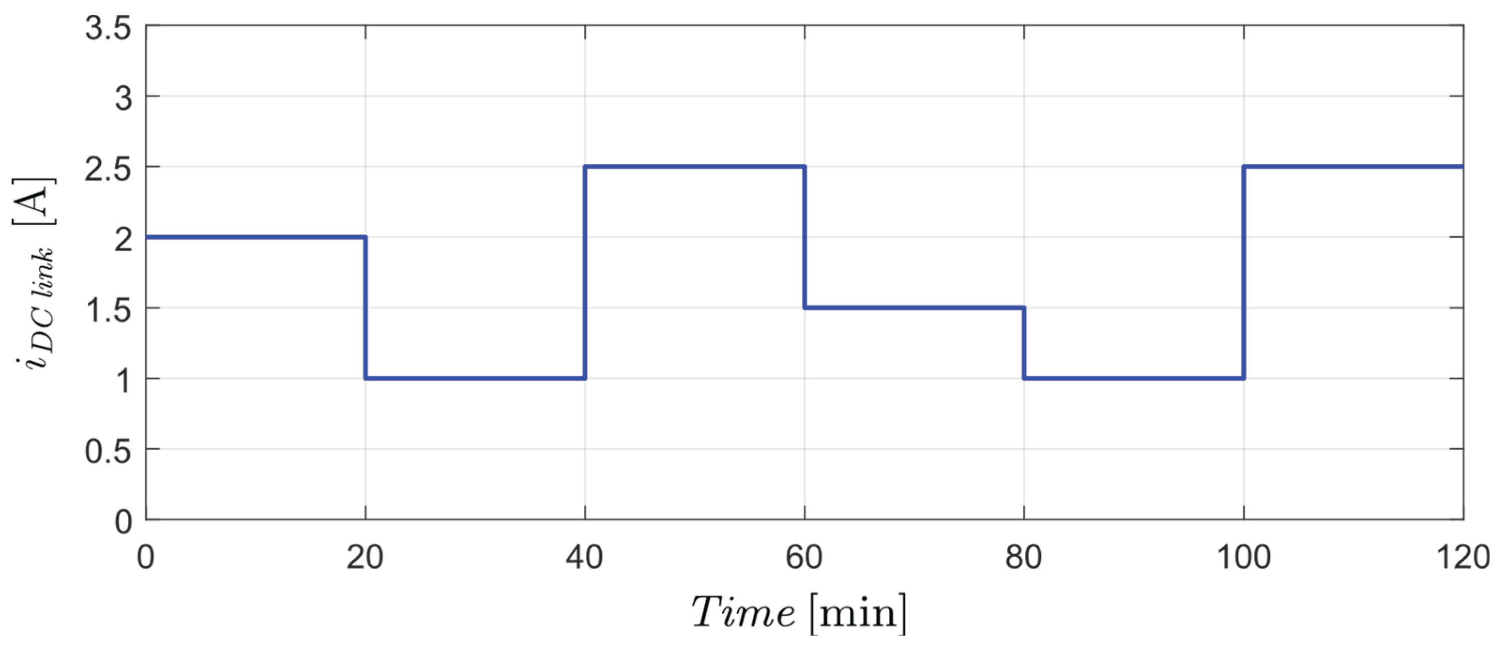
Figure A2.
Measurement results for the reference test set with branch rotation disabled, under the load profile defined in Figure A1.
Figure A2.
Measurement results for the reference test set with branch rotation disabled, under the load profile defined in Figure A1.
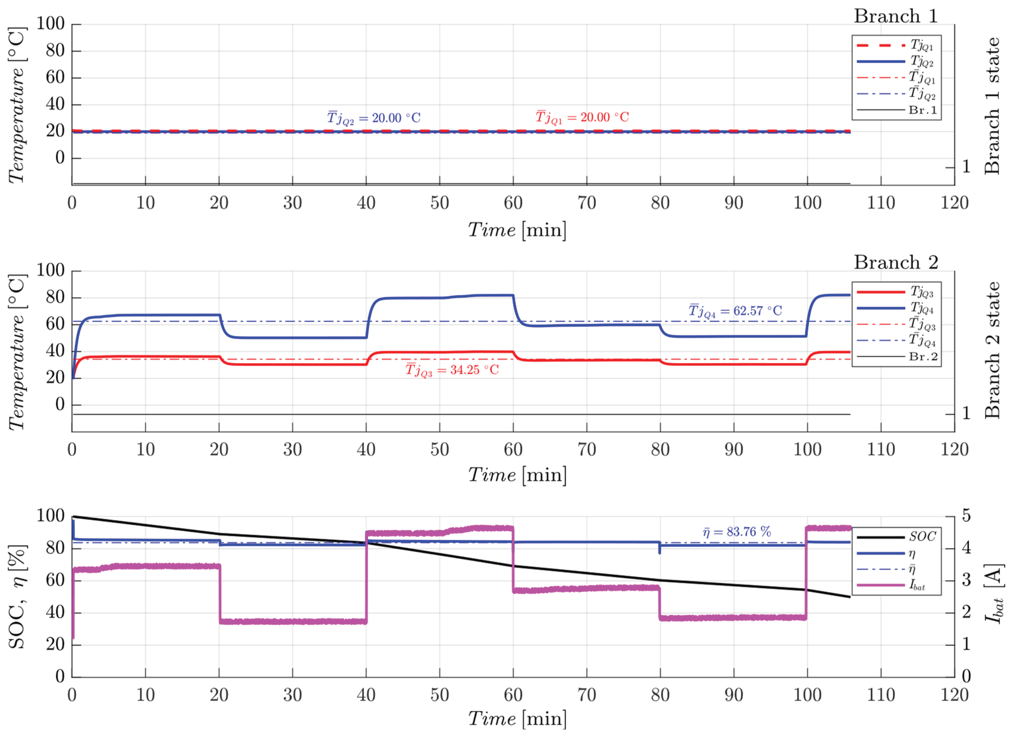
Figure A3.
Measurement results for the test set with a temperature threshold of , under the load profile shown in Figure A1.
Figure A3.
Measurement results for the test set with a temperature threshold of , under the load profile shown in Figure A1.
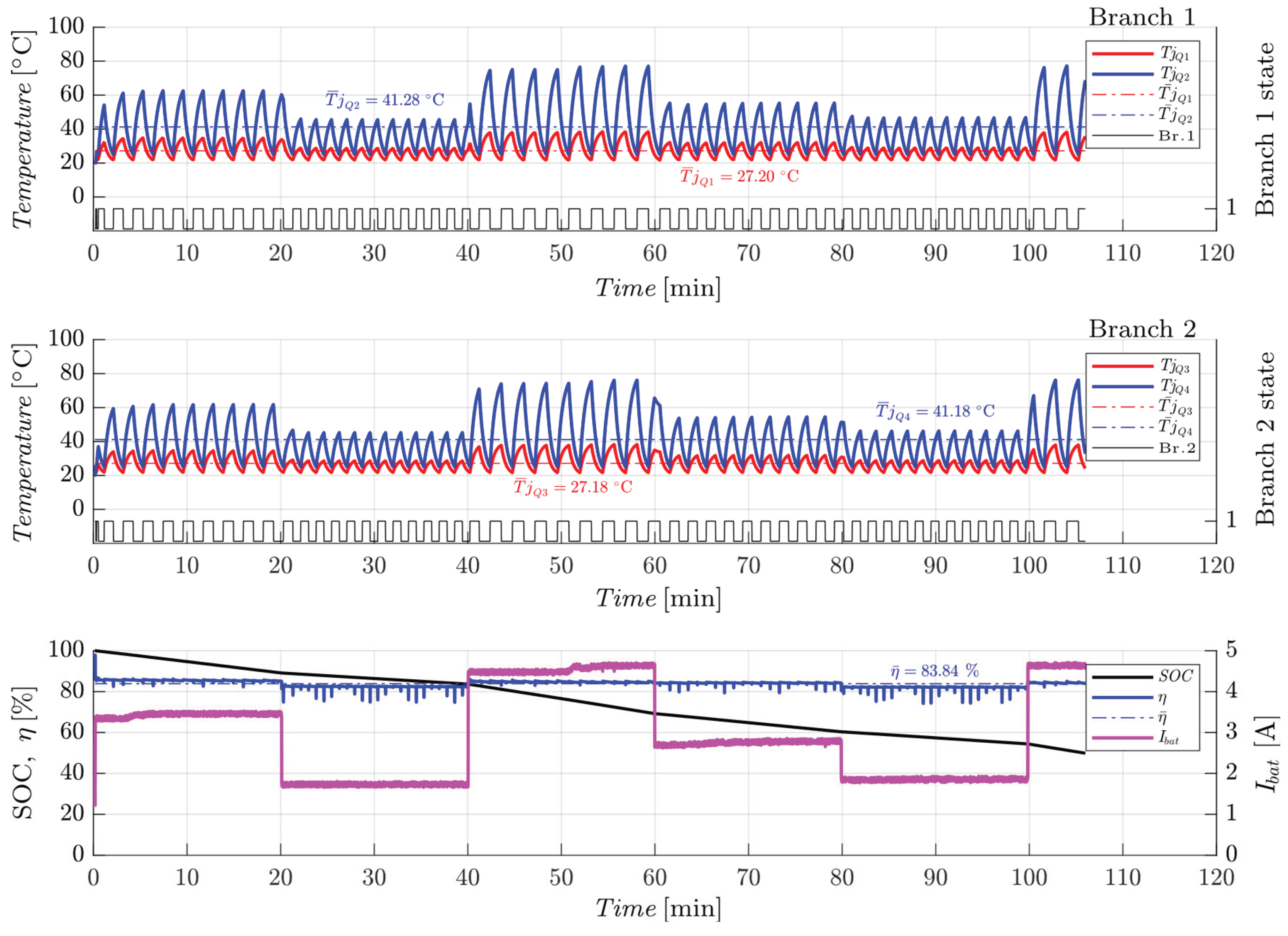
Figure A4.
Measurement results for the test set with a variable temperature threshold , under the load profile shown in Figure A1.
Figure A4.
Measurement results for the test set with a variable temperature threshold , under the load profile shown in Figure A1.
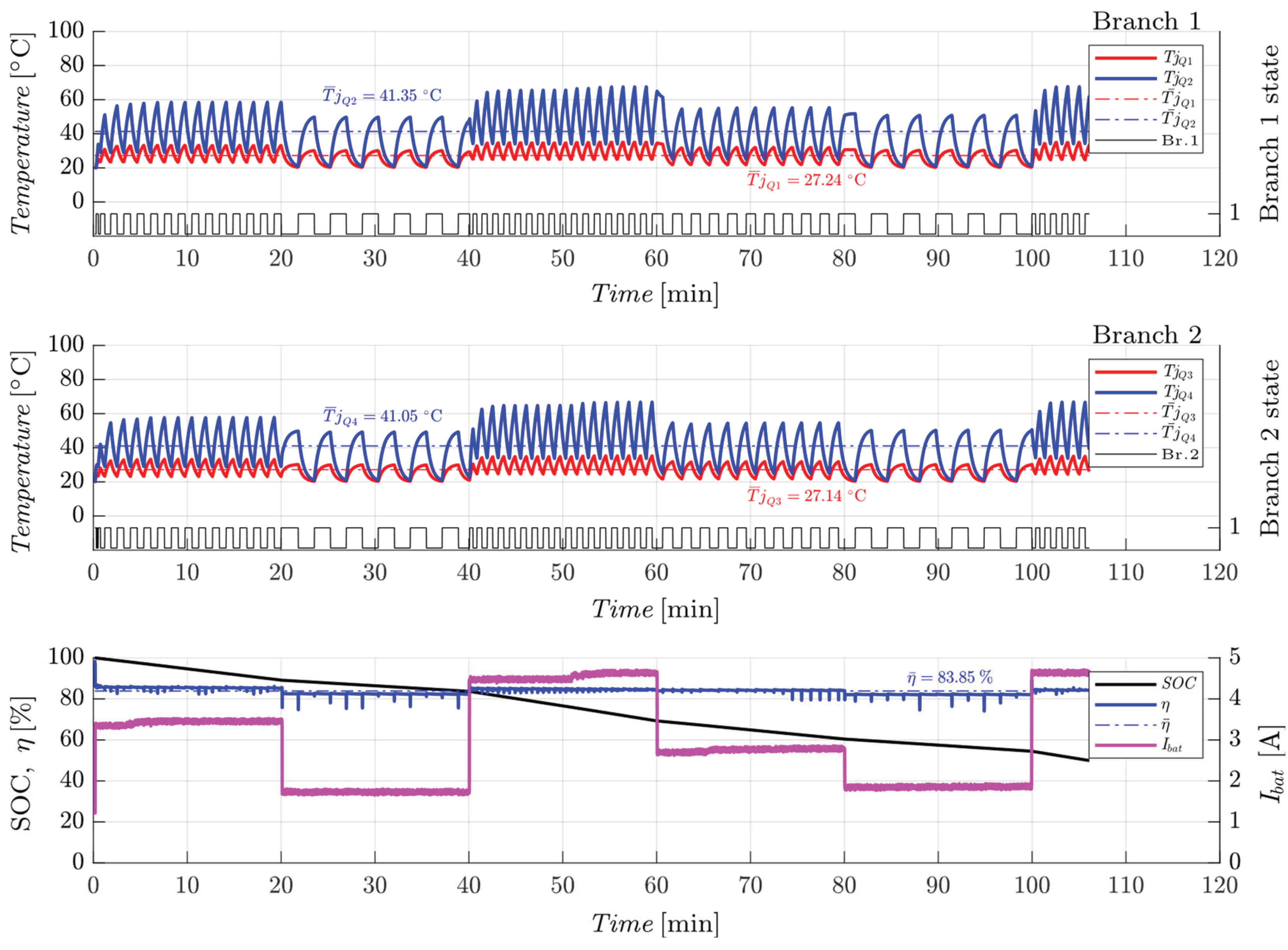

Table A1.
Summary of processed measurement results for boost mode operation, based on the results shown in Figure A2, Figure A3 and Figure A4.
| Branch, transistor | Branch 1, | Branch 2, | |||
| Temperature parameter | |||||
| Set 1 (reference) | |||||
| Set 2 | |||||
| Set 3 | |||||
| Relative temperature difference between measurement sets | |||||
| Time related parameters | |||||
| Set 1 (reference) | |||||
| Set 2 | |||||
| Set 3 | |||||
Figure A5.
Visual representation of the trends of the most relevant parameters during branch rotation, based on the data summarized in Table A1. (a) temperature related parameters; (b) time related parameters.
Figure A5.
Visual representation of the trends of the most relevant parameters during branch rotation, based on the data summarized in Table A1. (a) temperature related parameters; (b) time related parameters.
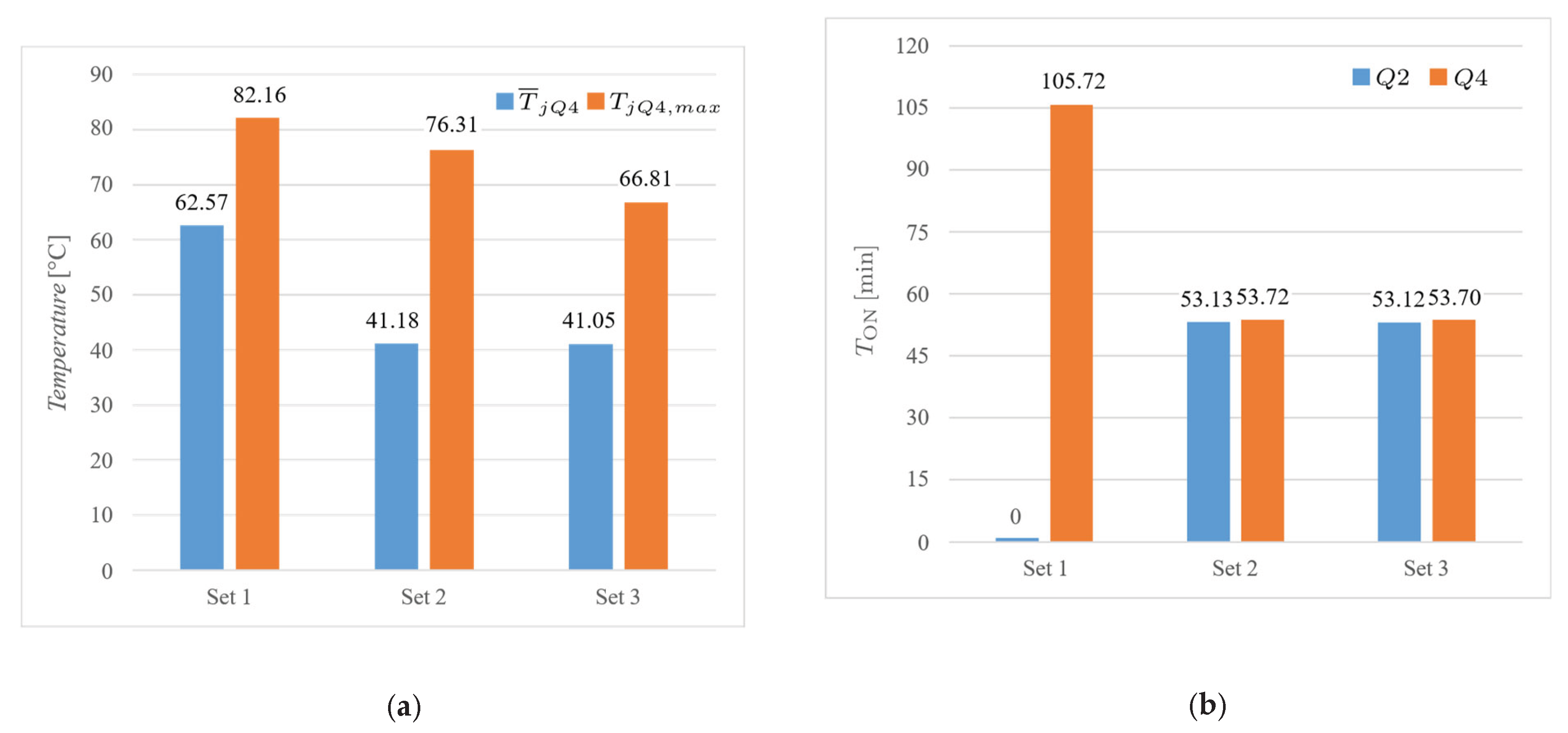
References
- Neware Five Major Functions of Battery Storage Systems. Available online: https://www.neware.net/news/five-major-functions-of-battery-storage-systems/230/57.html (accessed on 21 January 2026).
- Cole, W.; Karmakar, A. Cost Projections for Utility-Scale Battery Storage: 2023 Update. In Renewable Energy; 2023. [Google Scholar]
- FERIT Connected Stationary Battery Energy Storage. Available online: https://reslab.ferit.hr/?t=2&id=54 (accessed on 14 January 2026).
- Dharmasena, S.; Olowu, T.O.; Sarwat, A.I. Bidirectional AC/DC Converter Topologies: A Review. In Proceedings of the 2019 SoutheastCon, April 2019; IEEE: Huntsville, AL, USA; pp. 1–5. [Google Scholar]
- Kroics, K.; Husev, O.; Tytelmaier, K.; Zakis, J.; Veligorskyi, O. An Overview of Bidirectional AC-DC Grid Connected Converter Topologies for Low Voltage Battery Integration. IJPEDS 2018, 9, 1223. [Google Scholar] [CrossRef]
- Marei, M.I.; Alajmi, B.N.; Abdelsalam, I.; Ahmed, N.A. An Integrated Topology of Three-Port DC-DC Converter for PV-Battery Power Systems. IEEE Open J. Ind. Electron. Soc. 2022, 3, 409–419. [Google Scholar] [CrossRef]
- De Oliveira-Assis, L.; Soares-Ramos, E.P.P.; Sarrias-Mena, R.; García-Triviño, P.; González-Rivera, E.; Sánchez-Sainz, H.; Llorens-Iborra, F.; Fernández-Ramírez, L.M. Simplified Model of Battery Energy-Stored Quasi-Z-Source Inverter-Based Photovoltaic Power Plant with Twofold Energy Management System. Energy 2022, 244, 122563. [Google Scholar] [CrossRef]
- Wu, F.; Wang, K.; Hu, G.; Shen, Y.; Luo, S. Overview of Single-Stage High-Frequency Isolated AC–DC Converters and Modulation Strategies. IEEE Trans. Power Electron. 2023, 38, 1583–1598. [Google Scholar] [CrossRef]
- Brandis, A.; Knol, K.; Pelin, D.; Topić, D. Prototype Proposal of an 18 kW Non-Isolated Bidirectional Converter for Battery Energy Storage System. In Proceedings of the 2023 22nd International Symposium on Power Electronics (Ee), Novi Sad, Serbia, October 25 2023; IEEE; pp. 01–06. [Google Scholar]
- Fernão Pires, V.; Romero-Cadaval, E.; Vinnikov, D.; Roasto, I.; Martins, J.F. Power Converter Interfaces for Electrochemical Energy Storage Systems – A Review. Energy Conversion and Management 2014, 86, 453–475. [Google Scholar] [CrossRef]
- Xie, R.; Li, H.; Lin, B.; Xu, O.; Wang, X.; Han, Y.; Chen, J.; Xin, Z. Phase-Shedding Control in Two Parallel Interleaved Three-Phase ZVS Inverters for Improved Light Load Efficiency. IEEE Access 2023, 11, 77793–77801. [Google Scholar] [CrossRef]
- Su, J.-T.; Liu, C.-W. A Novel Phase-Shedding Control Scheme for Improved Light Load Efficiency of Multiphase Interleaved DC–DC Converters. IEEE Trans. Power Electron. 2013, 28, 4742–4752. [Google Scholar] [CrossRef]
- Costabeber, A.; Mattavelli, P.; Saggini, S. Digital Time-Optimal Phase Shedding in Multiphase Buck Converters. IEEE Trans. Power Electron. 2010, 25, 2242–2247. [Google Scholar] [CrossRef]
- Zumel, P.; Fernández, C.; De Castro, A.; García, O. Efficiency Improvement in Multiphase Converter by Changing Dynamically the Number of Phases. In Proceedings of the 2006 37th IEEE Power Electronics Specialists Conference, June 2006; IEEE: Jeju, Korea (South); pp. 1–6. [Google Scholar]
- Alharbi, M.A.; Dahidah, M.; Ethni, S.; Ali, S.; Kadandani, N.B.; Pickert, V. A Phase Shedding Control Technique for Ripple Minimisation for EV Fast DC Charging Applications. In Proceedings of the 2021 23rd European Conference on Power Electronics and Applications (EPE’21 ECCE Europe), Ghent, Belgium, September 6 2021; IEEE; pp. 1–10. [Google Scholar]
- Lim, H.; Jang, M.; Agelidis, V. A Phase Shedding Technique for PV System Based on Interleaved Boost Converter. In Proceedings of the 2015 IEEE 2nd International Future Energy Electronics Conference (IFEEC), November 2015; IEEE: Taipei, Taiwan; pp. 1–5. [Google Scholar]
- Lee, J.-S.; Huang, C.-Y.; Liang, T.-J.; Chen, K.-H. Design of Control IC for Multiphase Interleaved Buck Converter with Alternate Phase-Shedding. In Proceedings of the 2015 9th International Conference on Power Electronics and ECCE Asia (ICPE-ECCE Asia), June 2015; IEEE: Seoul, South Korea; pp. 1025–1032. [Google Scholar]
- Lin, J.-T.; Hu, K.; Tsai, C.-H. Digital Multiphase Buck Converter with Current Balance/Phase Shedding Control. In Proceedings of the TENCON 2015 - 2015 IEEE Region 10 Conference, November 2015; IEEE: Macao; pp. 1–5. [Google Scholar]
- Nkembi, A.A.; Santoro1, D.; Kortabarria, I.; Cova, P.; Delmonte, N.; Sacchi, E. An Adaptive Phase Shedding and Interleaving Technique for Modular Dual Active Bridge Converter Applied to Fast Battery Charging. IET Conf. Proc. 2025, 2024, 47–52. [Google Scholar] [CrossRef]
- Mao, G.; Zhou, G.; Zhao, H.; Gao, Y.; Kubulus, P.P.; Munk-Nielsen, S. Digital Average Current Predictive Control for Multiphase Interleaved DC–DC Converters. IEEE Trans. Circuits Syst. II 2023, 70, 4519–4523. [Google Scholar] [CrossRef]
- Alharbi, M.A.; Alcaide, A.M.; Dahidah, M.; M.-R., P.; Ethni, S.; Pickert, V.; Leon, J.I. Rotating Phase Shedding for Interleaved DC–DC Converter-Based EVs Fast DC Chargers. IEEE Trans. Power Electron. 2023, 38, 1901–1909. [Google Scholar] [CrossRef]
- Yedukondalu, G.; Samanta, S. Effective Phase Utilization and Efficiency Improvement of High Power Interleaved DC–DC Converter Using Modified Rotating Phase Shedding Control. Computers and Electrical Engineering 2023, 110, 108837. [Google Scholar] [CrossRef]
- Xiao, Z.; Yao, Z.; Deng, F.; Zhang, L.; Tang, Y. Seamless Rotational Phase Shedding for Multiphase DC–DC Converters. IEEE Trans. Power Electron. 2024, 39, 4996–5001. [Google Scholar] [CrossRef]
- Zhang, X.; Zhang, G.; Yu, S.S. Review of Control Techniques for Interleaved Buck Converters: Control Strategies, Efficiency Optimization and Phase Shedding. Chin. J. Electr. Eng. 2025, 1–19. [Google Scholar] [CrossRef]
- Brandis, A.; Knol, K.; Pelin, D. Current-Adaptive Control for Efficiency Enhancement in Interleaved Converters for Battery Energy Storage Systems. Electronics 2025, 14, 1862. [Google Scholar] [CrossRef]
- Typhoon HIL HIL402 Hardware User Guide. Available online: https://www.typhoon-hil.com/documentation/typhoon-hil-hardware-manual/hil402_user_guide/topics/hil402_abstract.html (accessed on 7 January 2026).
- Real-Time Simulation and Hardware-in-the-Loop Testing Using Typhoon HIL. In Transactions on Computer Systems and Networks; Tripathi, S.M., Gonzalez-Longatt, F.M., Eds.; Springer Nature Singapore: Singapore, 2023; ISBN 978-981-99-0223-1. [Google Scholar]
- Texas Instruments F28379D Development Kit for C2000TM Delfino MCU controlCARDTM. Available online: https://www.ti.com/tool/TMDSCNCD28379D (accessed on 21 February 2026).
- Brandis, Andrej. Typhoon HIL 402 Simulation Platform for Interleaved Converters with Selectable Efficiency-Oriented Control Algorithms Applied to Battery Energy Storage Systems 2025.
- Tesla, Inc. Tesla Powerwall. Available online: https://www.tesla.com/powerwall (accessed on 19 November 2025).
- Jokar, M.; Ghani, P.; Babaei, S.; Hafezi, H.R.; Abbasi, M.; Sadeghi, R. Design and Implementation of a 3 kW Single-Phase BESS Using ARM & FPGA. In Proceedings of the 2019 10th International Power Electronics, Drive Systems and Technologies Conference (PEDSTC), February 2019; IEEE: Shiraz, Iran; pp. 389–394. [Google Scholar]
- Jiangsu KOYOE Energy Technology Co; Ltd. User Manual: Energy Storage Inverter KY-1Hybrid-5k0-H 2025.
- Brand, M.J.; Hofmann, M.H.; Schuster, S.S.; Keil, P.; Jossen, A. The Influence of Current Ripples on the Lifetime of Lithium-Ion Batteries. IEEE Trans. Veh. Technol. 2018, 67, 10438–10445. [Google Scholar] [CrossRef]
- Taghizadeh, S.; Hossain, M.J.; Lu, J.; Water, W. A Unified Multi-Functional on-Board EV Charger for Power-Quality Control in Household Networks. Applied Energy 2018, 215, 186–201. [Google Scholar] [CrossRef]
- Rachmad, R.W.; Abuzairi, T. Efficiency Comparison of Asynchronous and Synchronous Buck Converter with Variation in Duty Cycle and Output Current. Buletin Ilmiah Sarjana Teknik Elektro 2023, 5, 41–55. [Google Scholar] [CrossRef]
- Brandis, Andrej. Increasing the efficiency of a multi-branch DC converter for stationary battery energy storage by changing the number of active branches. Doctoral thesis, University of Josip Juraj Strossmayer in Osijek, Osijek, 2024. [Google Scholar]
- Setiawan, I.; Facta, M.; Andromeda, T.; Hermawan, H.; Syakur, A. Unified and Separated Buck/Boost Averaged Current Control Strategies of Bidirectional DC-DC Converter for DC Microgrid Systems. IREACO 2022, 15, 204. [Google Scholar] [CrossRef]
- Lee, H.-S.; Yun, J.-J. High-Efficiency Bidirectional Buck–Boost Converter for Photovoltaic and Energy Storage Systems in a Smart Grid. IEEE Trans. Power Electron. 2019, 34, 4316–4328. [Google Scholar] [CrossRef]
- Laoprom, I.; Tunyasrirut, S. Design of PI Controller for Voltage Controller of Four-Phase Interleaved Boost Converter Using Particle Swarm Optimization. Journal of Control Science and Engineering 2020, 2020, 1–13. [Google Scholar] [CrossRef]
- Rossi, D.; Tenentes, V. Run-Time Thermal Management for Lifetime Optimization in Low-Power Designs. Electronics 2022, 11, 411. [Google Scholar] [CrossRef]
- Kong, K.; Choi, J.; Park, G.; Baek, S.; Ju, S.; Han, Y. Insulated Gate Bipolar Transistor Junction Temperature Estimation Technology for Traction Inverters Using a Thermal Model. Electronics 2025, 14, 999. [Google Scholar] [CrossRef]
- Morel, C.; Morel, J.-Y. Power Semiconductor Junction Temperature and Lifetime Estimations: A Review. Energies 2024, 17, 4589. [Google Scholar] [CrossRef]
- Zhang, J.; Shen, H.; Sun, H.; Wang, Z. Review on the Thermal Models Applications in the Reliability of Power Semiconductor Device. IET Power Electronics 2025, 18, e70065. [Google Scholar] [CrossRef]
- STMicroelectronics VNP10N07 – Smart Power MOSFET for Automotive Applications. Available online: https://www.st.com/en/automotive-analog-and-power/vnp10n07.html (accessed on 14 May 2025).
- Wakefield Thermal Wakefield-Vette Heatsink.
Figure 1.
Normalized capital cost projections for utility-scale 4-hour lithium-ion battery storage systems from 2022 to 2050, based on low, mid, and high scenarios based on NREL’s 2023 report.
Figure 1.
Normalized capital cost projections for utility-scale 4-hour lithium-ion battery storage systems from 2022 to 2050, based on low, mid, and high scenarios based on NREL’s 2023 report.
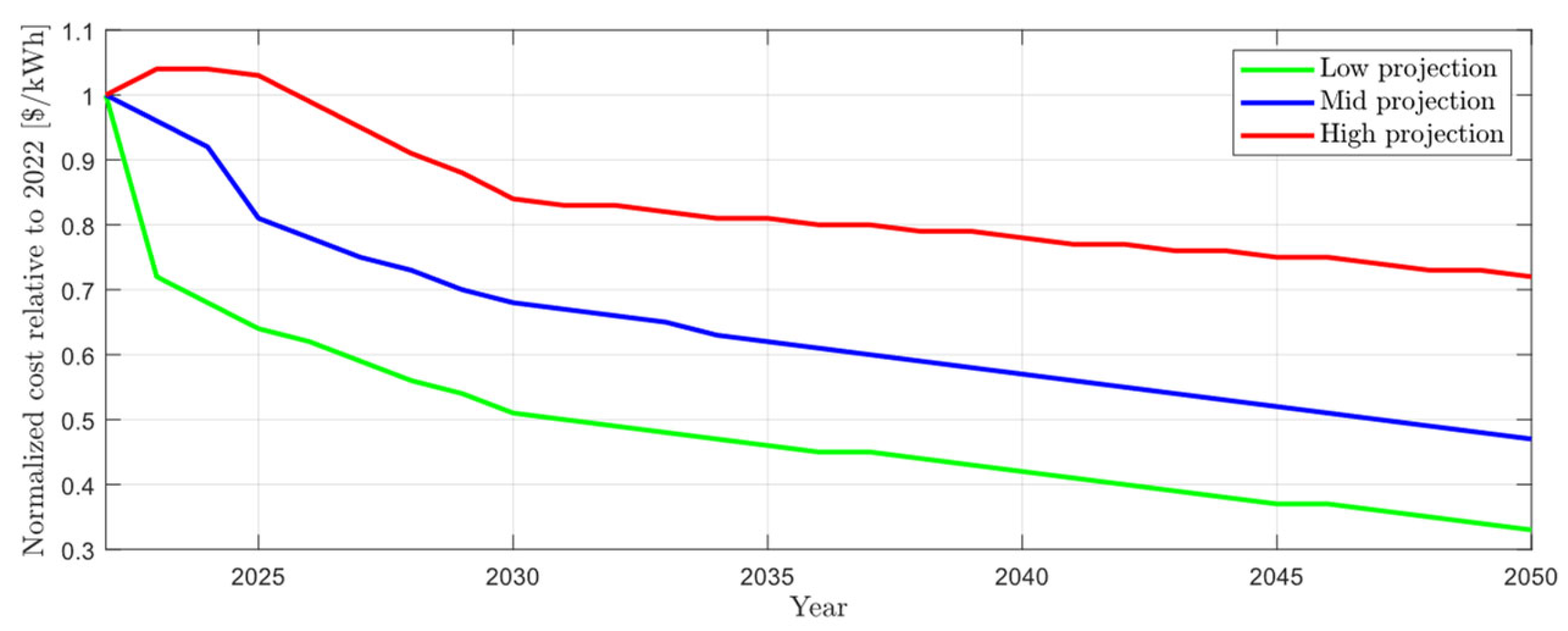
Figure 2.
Block diagram of a networked stationary battery energy storage system.
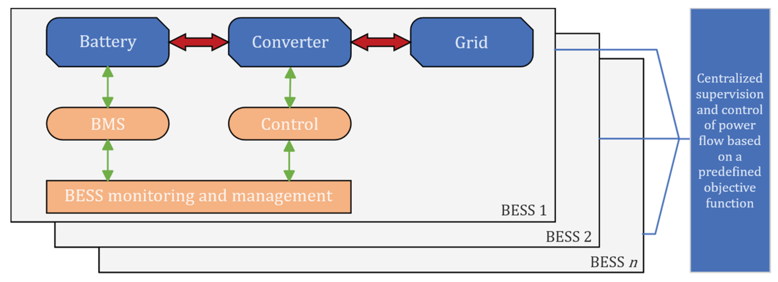
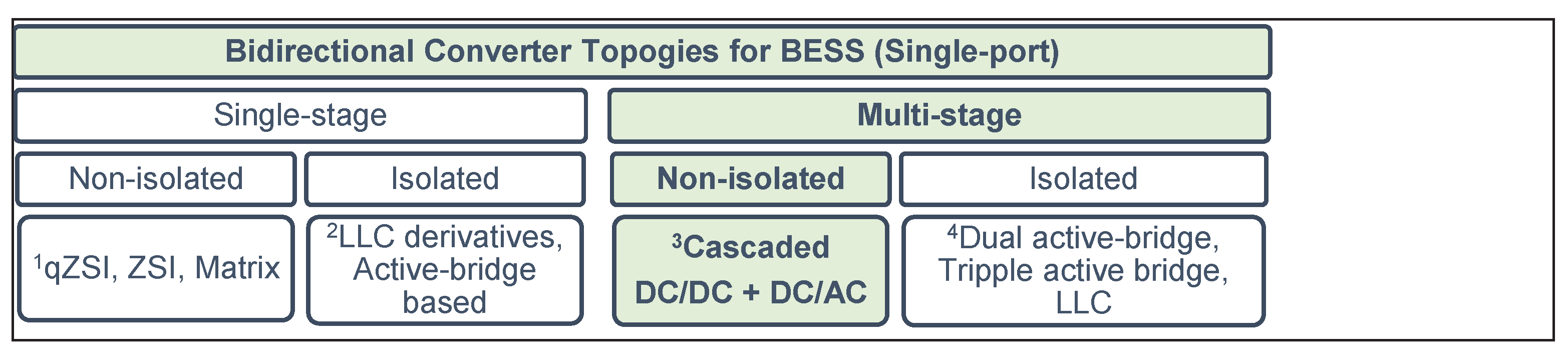
Figure 4.
Bidirectional non-isolated converter in a two-stage conversion topology.
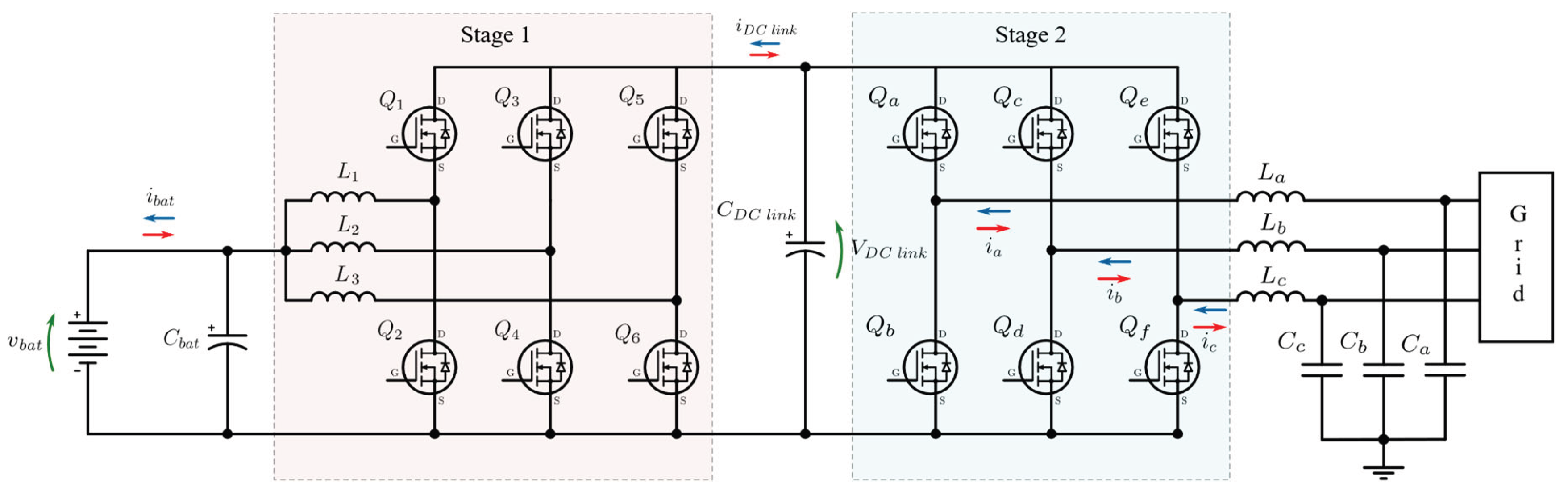
Figure 5.
Methodologies used for power electronics converter development.
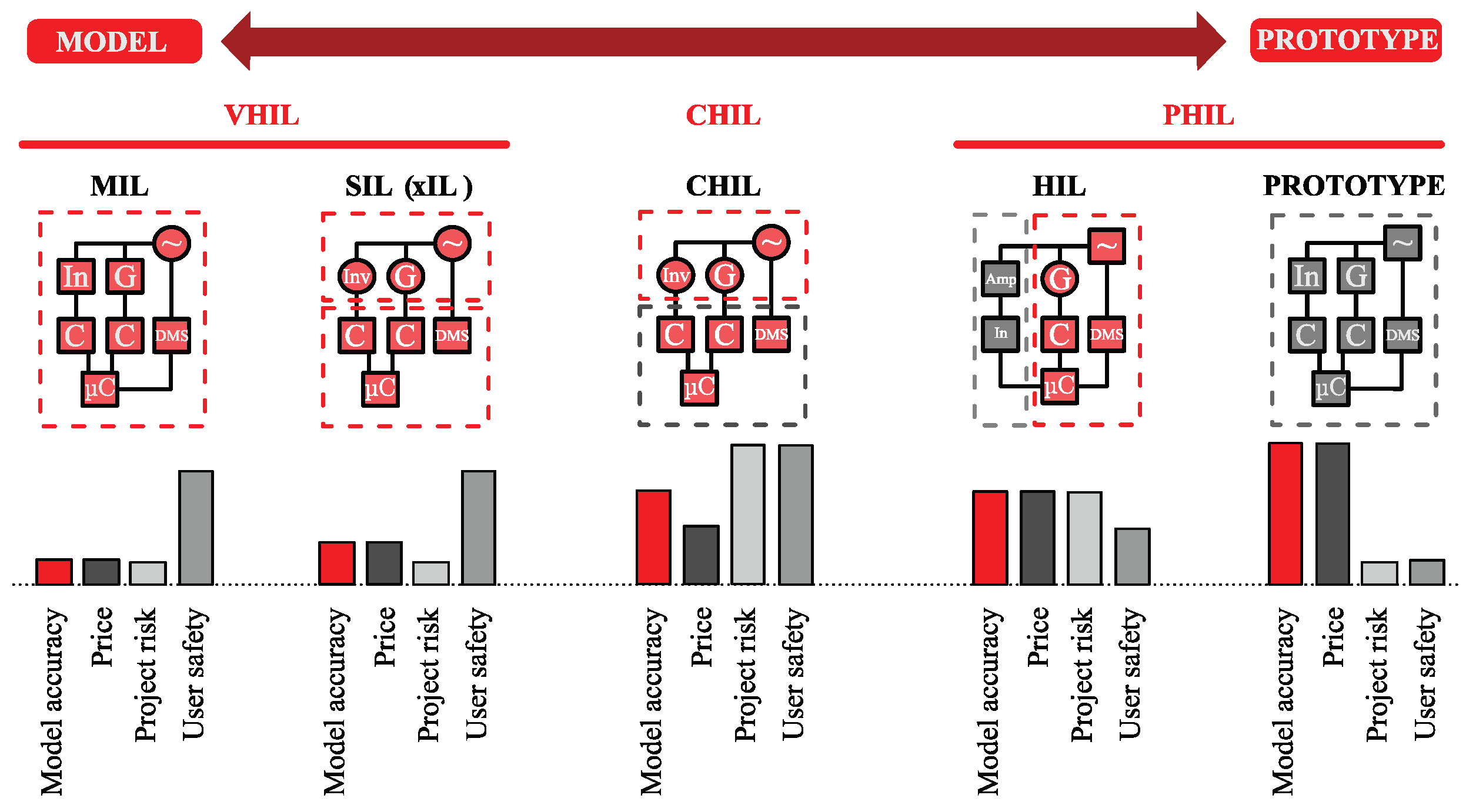
Figure 6.
Typhoon HIL 402 hardware (1) equipped with the DSP Interface 3.1 for external microcontroller units (2), a 180-pin Texas Instruments TMS320F28379D DSP card inserted (3) (a). Basic microcontroller architecture of the Typhoon HIL 402 system (b).
Figure 6.
Typhoon HIL 402 hardware (1) equipped with the DSP Interface 3.1 for external microcontroller units (2), a 180-pin Texas Instruments TMS320F28379D DSP card inserted (3) (a). Basic microcontroller architecture of the Typhoon HIL 402 system (b).
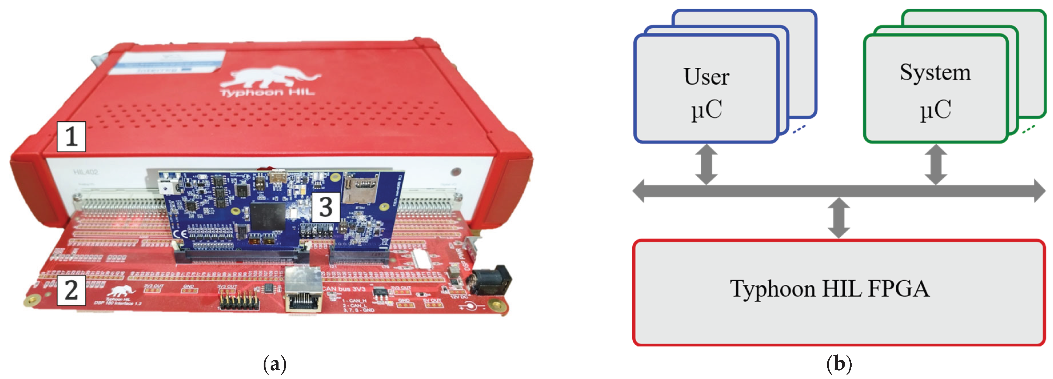
Figure 7.
Developed signal routing enabling the use of the internal microcontroller for control implementation.
Figure 7.
Developed signal routing enabling the use of the internal microcontroller for control implementation.
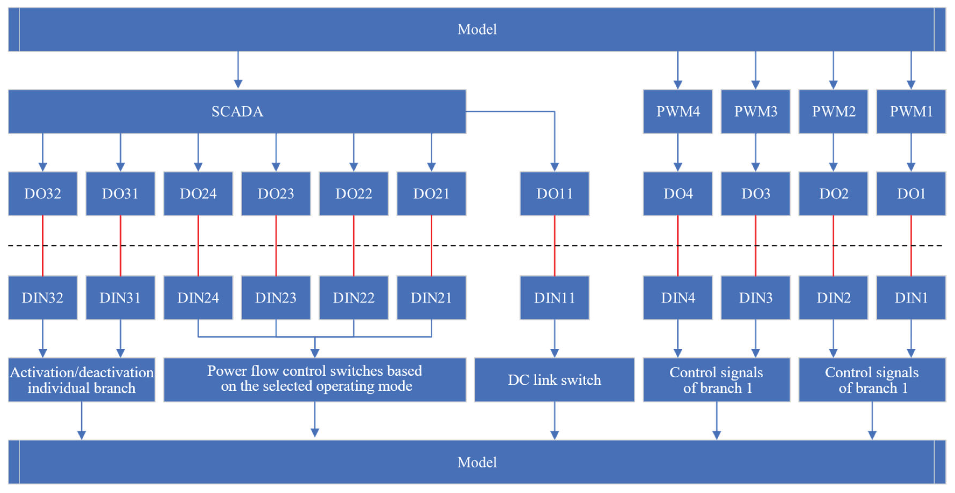
Figure 8.
Converter development flowchart.
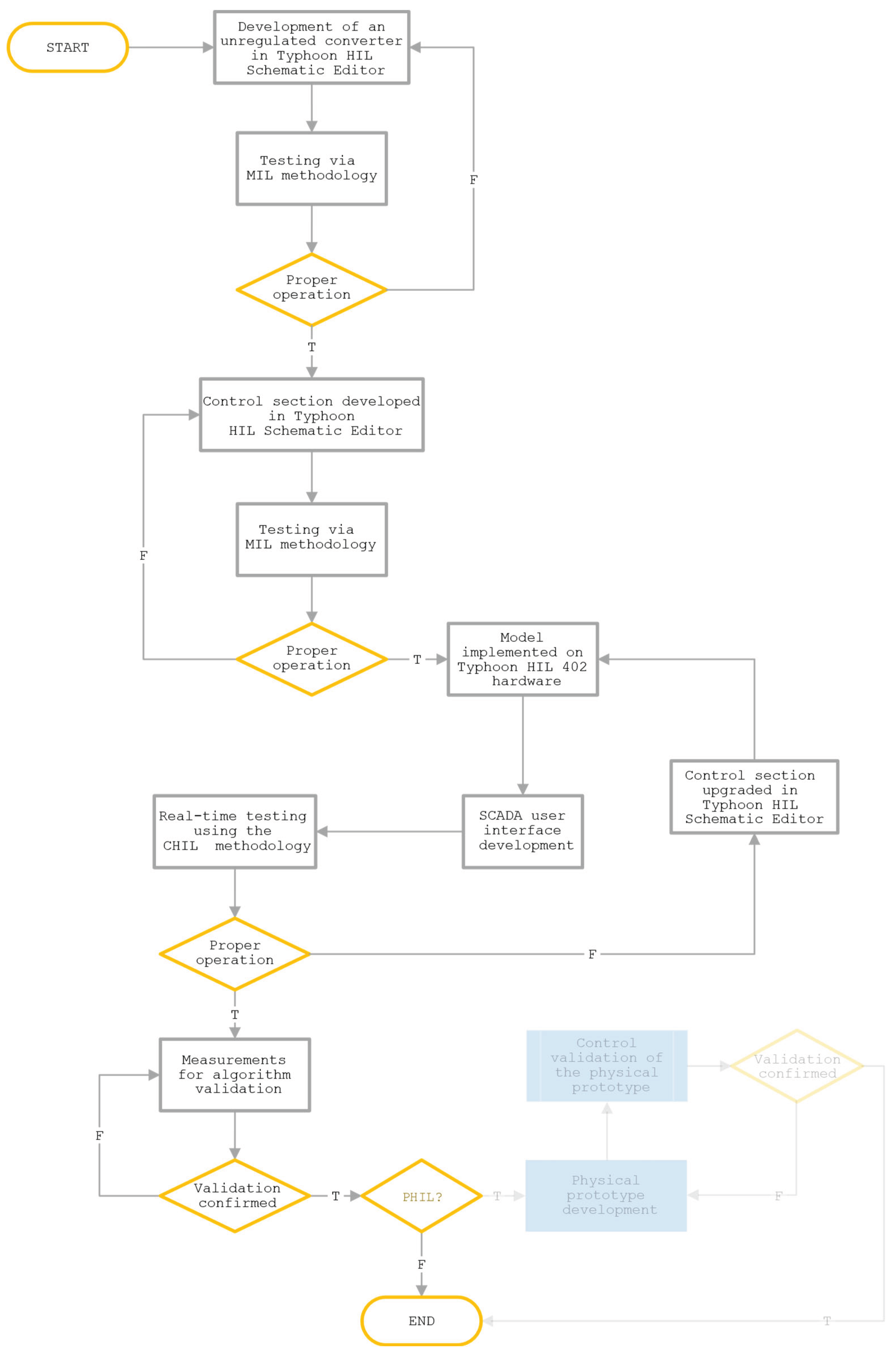
Figure 9.
SCADA system used as a user interface for managing the entire system, including the microcontroller, and for data acquisition.
Figure 9.
SCADA system used as a user interface for managing the entire system, including the microcontroller, and for data acquisition.
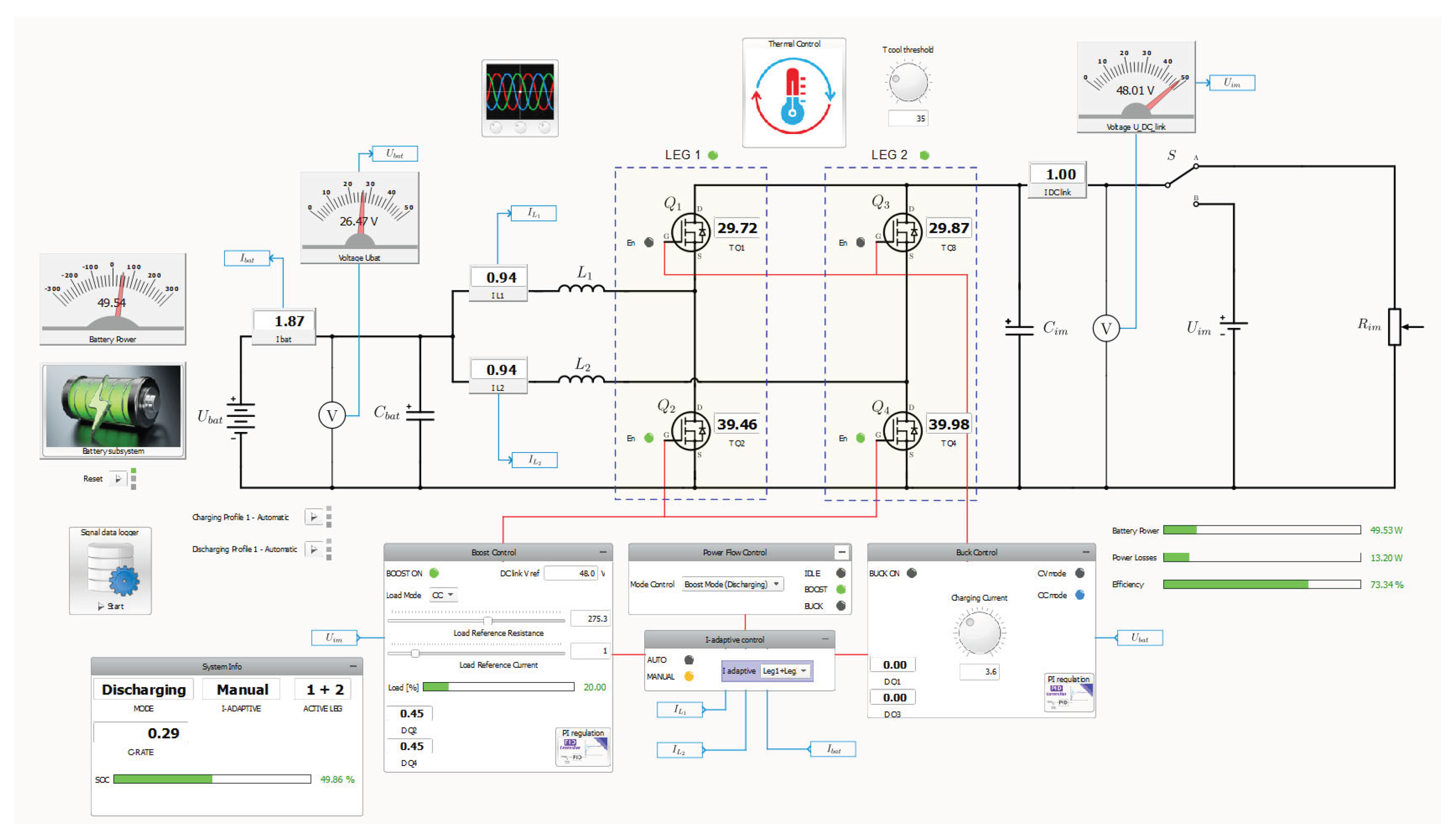
Figure 10.
Screenshot of open-loop simulation model of a two-branch DC-DC converter in Typhoon HIL environment.
Figure 10.
Screenshot of open-loop simulation model of a two-branch DC-DC converter in Typhoon HIL environment.
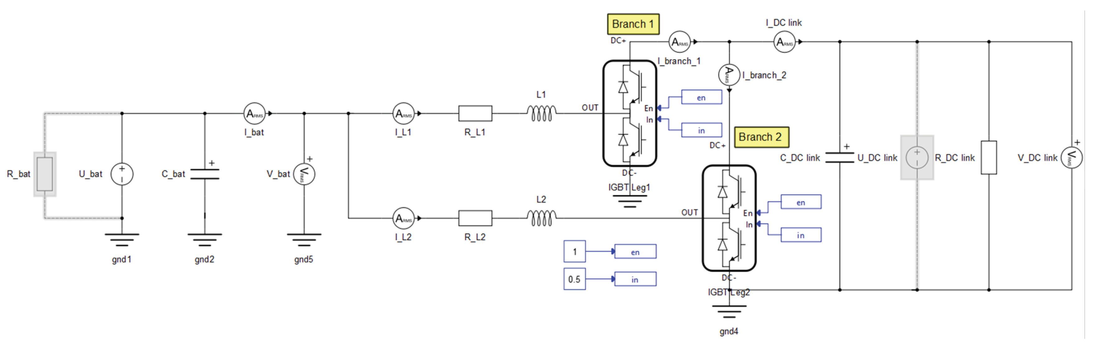
Figure 11.
Boost mode simulation results according to the markings in Figure 10: simulation instrument readings of input and output values (a), and selected recorded waveforms (b).
Figure 11.
Boost mode simulation results according to the markings in Figure 10: simulation instrument readings of input and output values (a), and selected recorded waveforms (b).
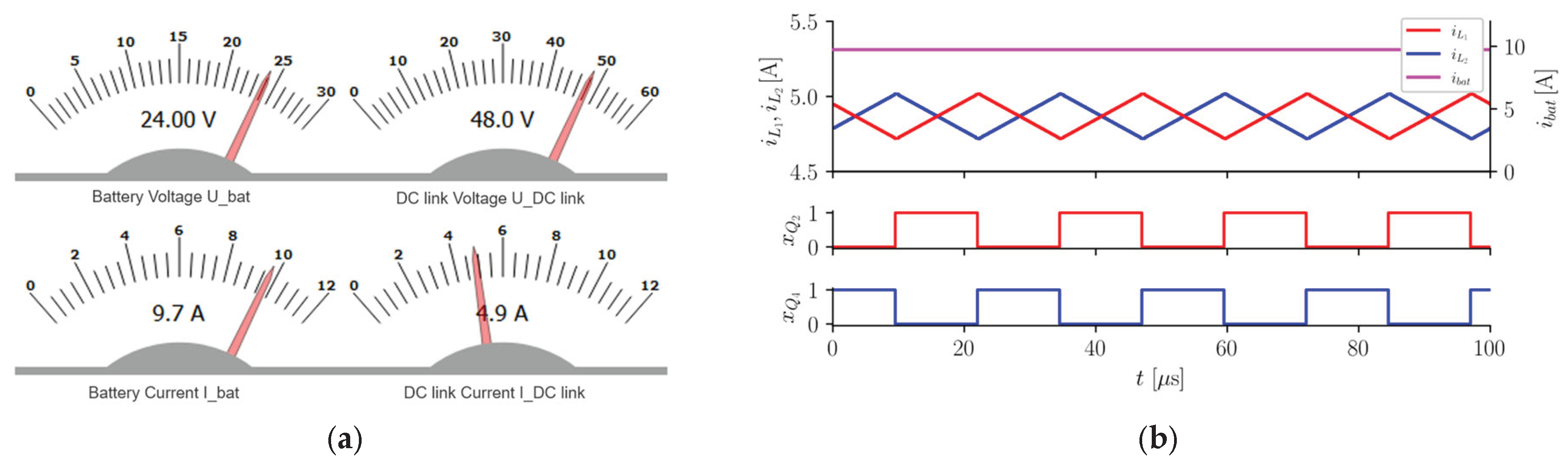
Figure 12.
Simplified block diagram of a two-branch BIC system simulation model.
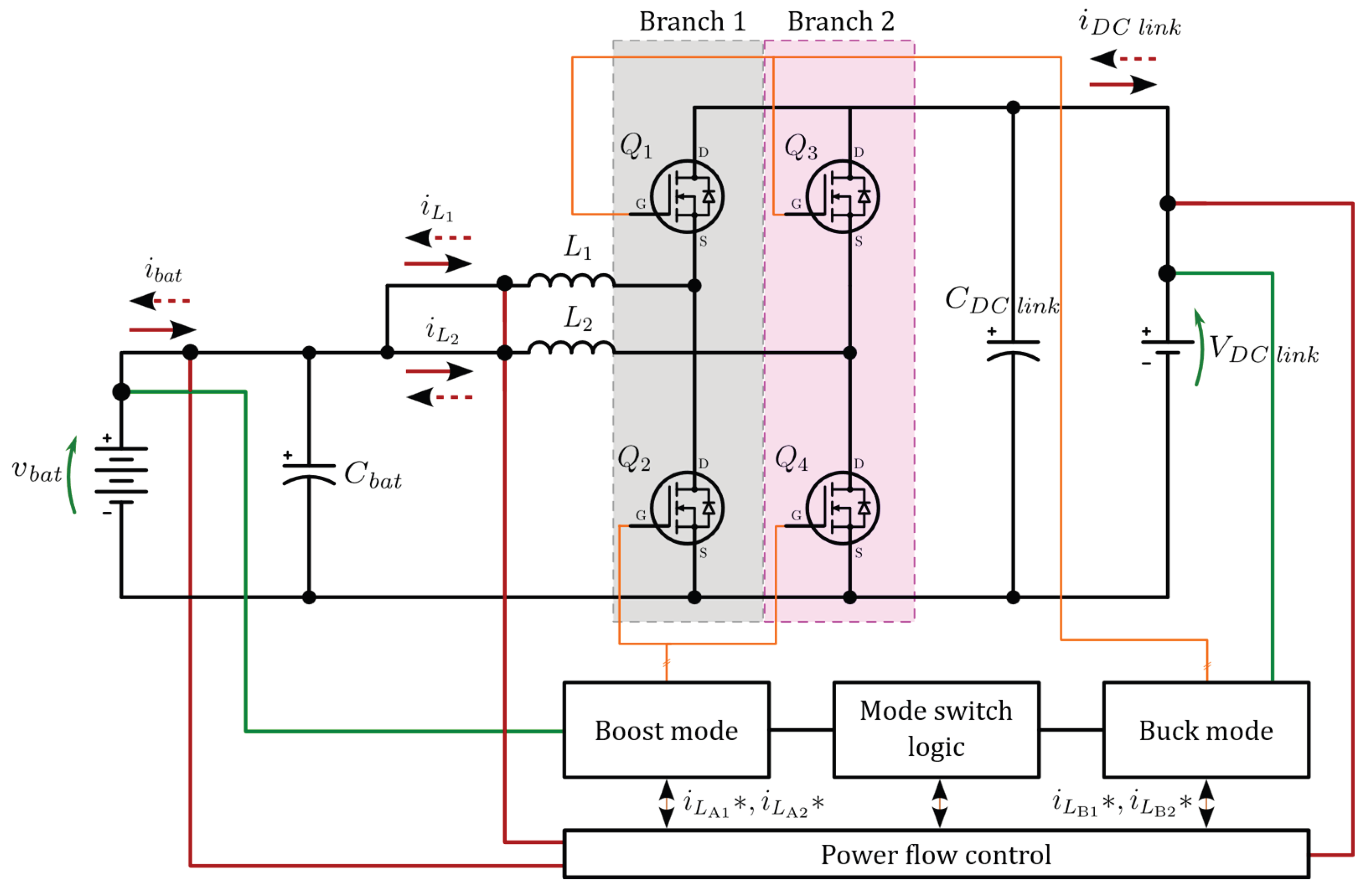
Figure 13.
The relationship between: (a) asynchronous control and (b) charge/discharge regulators characteristics of the battery (separated regulators).
Figure 13.
The relationship between: (a) asynchronous control and (b) charge/discharge regulators characteristics of the battery (separated regulators).
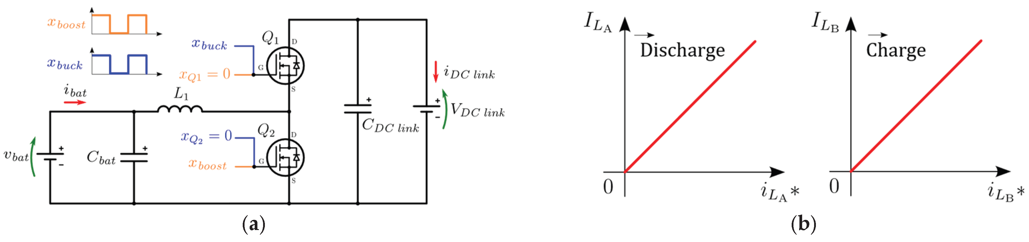
Figure 14.
Dual-loop control of a two-branch BIC implemented in Typhoon HIL.
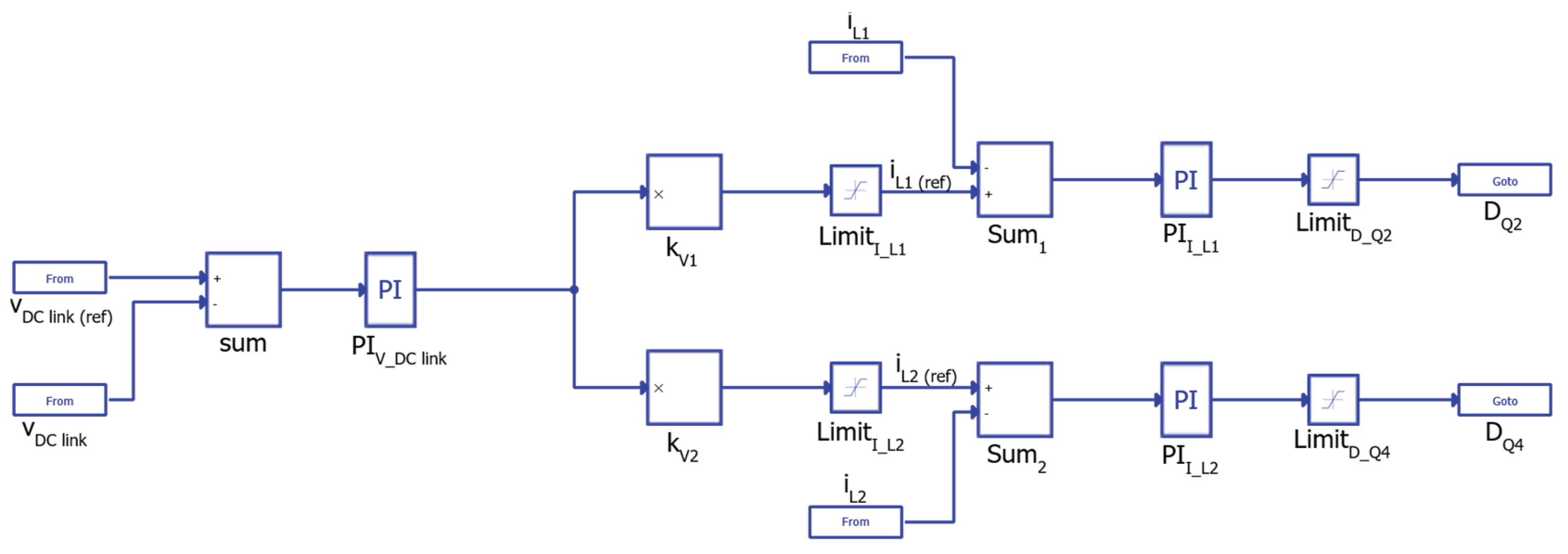
Figure 15.
Illustration of heat dissipation in an electronic component.
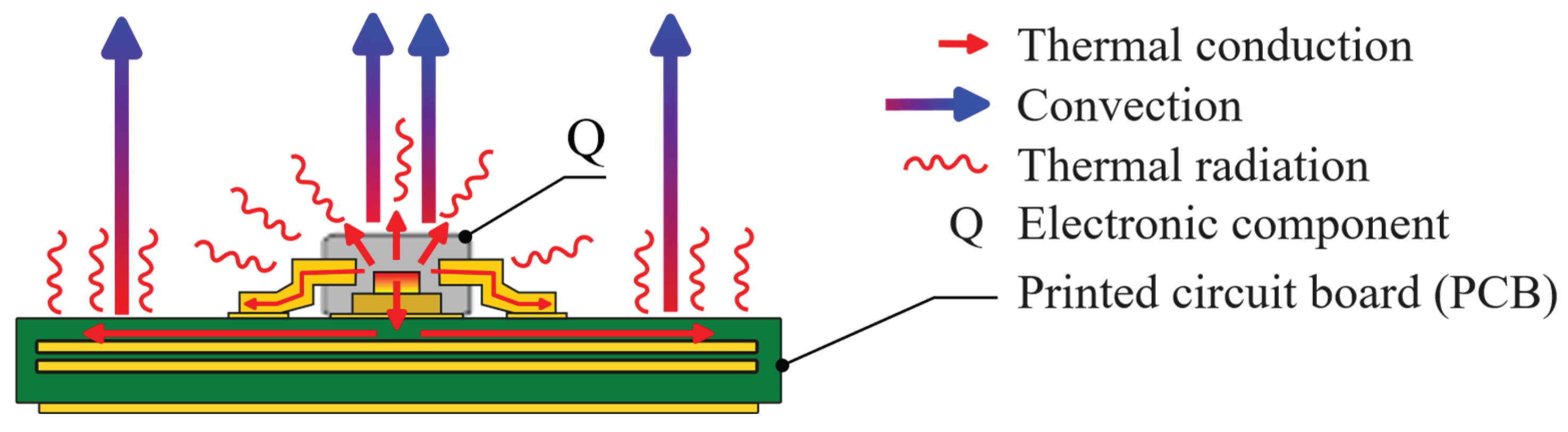
Figure 16.
Illustration of the Cauer model for a single branch of a BIC.
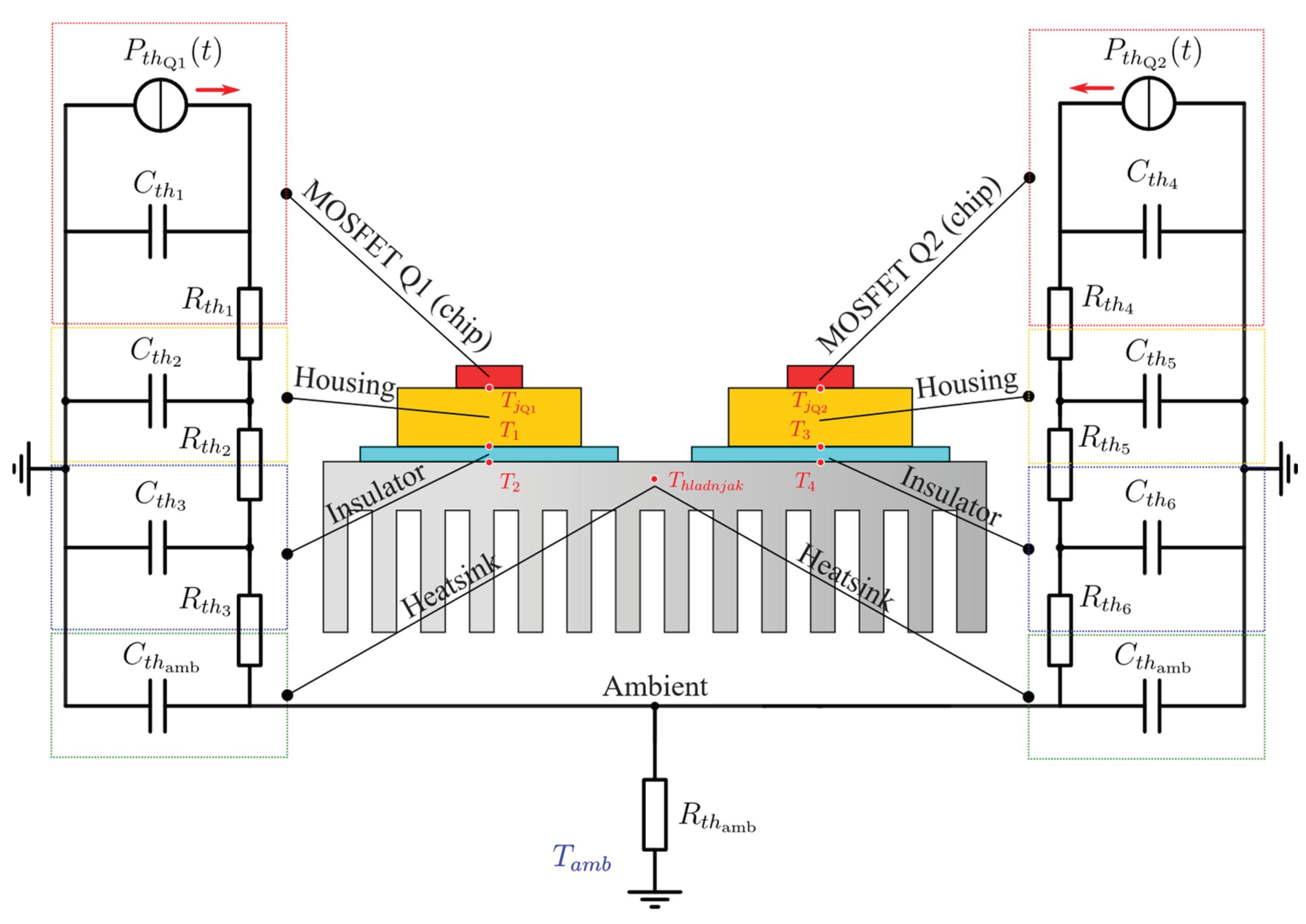
Figure 17.
Thermal parametrization of: (a) interface for defining the thermal model parameters of the switching components; (b) single BIC branch with a heat sink parameter interface.
Figure 17.
Thermal parametrization of: (a) interface for defining the thermal model parameters of the switching components; (b) single BIC branch with a heat sink parameter interface.
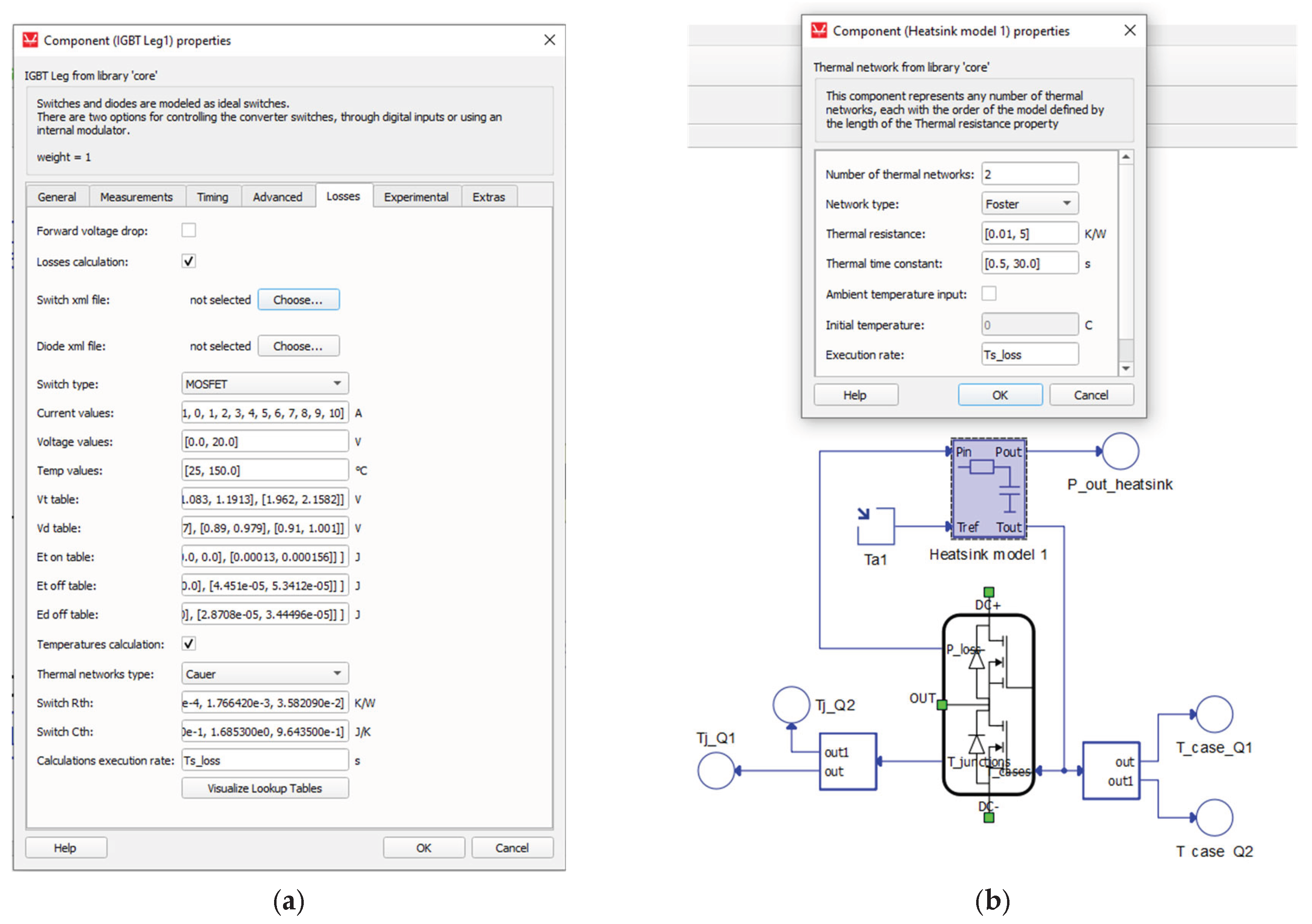
Figure 18.
Representation of a two-dimensional vector (a), and a three-dimensional vector (b), used for calculating conduction and switching losses in the simulation model.
Figure 18.
Representation of a two-dimensional vector (a), and a three-dimensional vector (b), used for calculating conduction and switching losses in the simulation model.
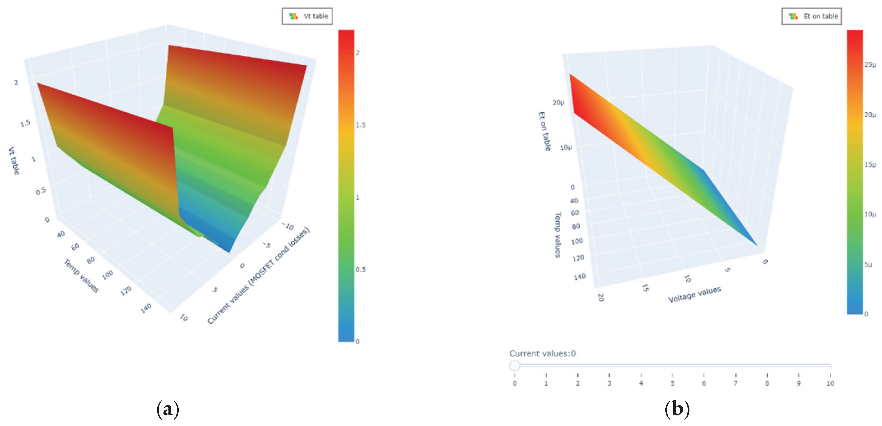
Figure 19.
Simulation results of converter efficiency and losses as a function of the number of active branches in: (a) boost operation, and (b) buck operation.
Figure 19.
Simulation results of converter efficiency and losses as a function of the number of active branches in: (a) boost operation, and (b) buck operation.
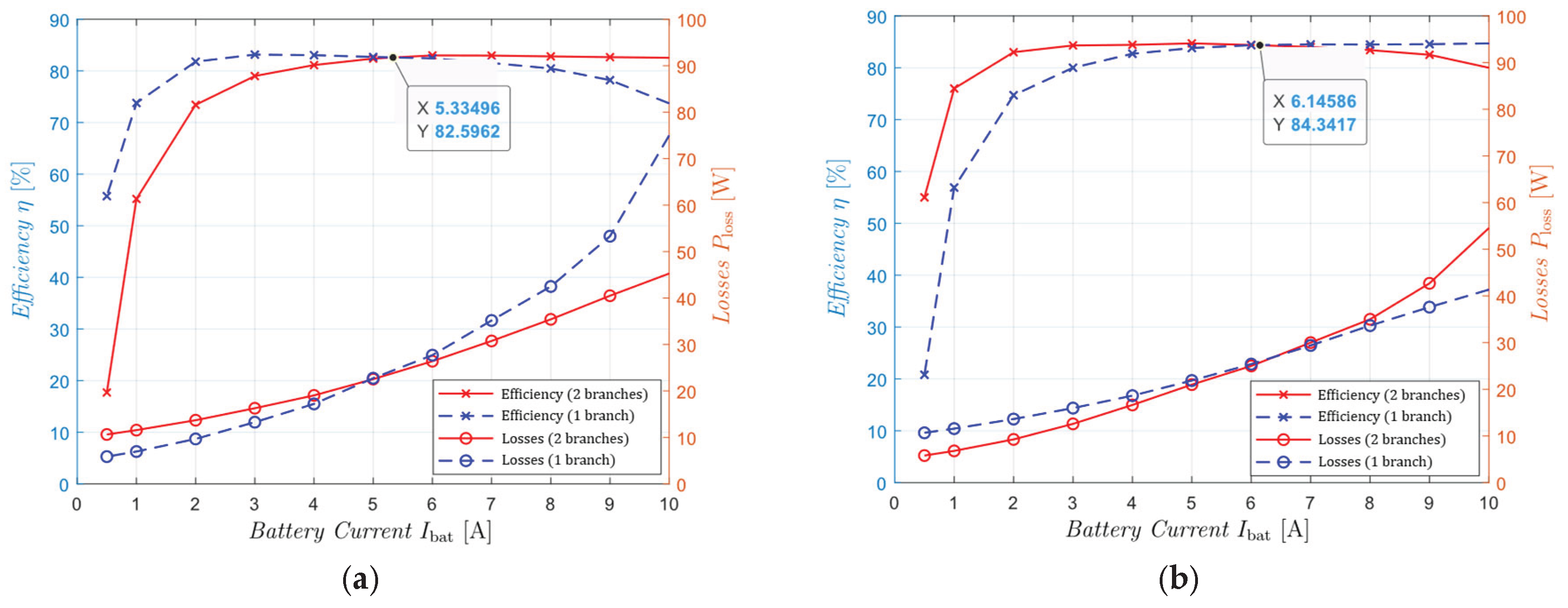
Figure 20.
Current-adaptive algorithm flowchart.
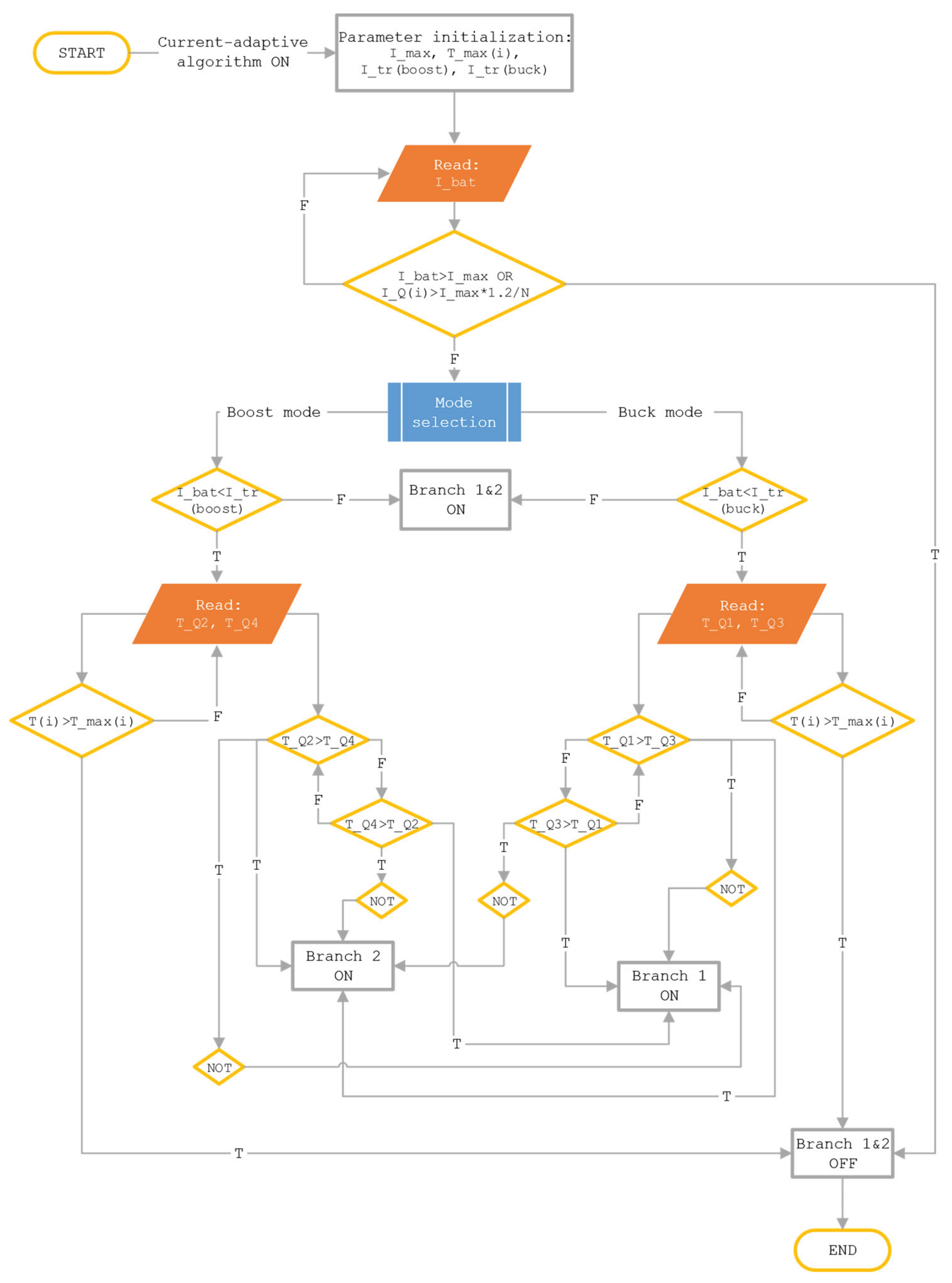
Figure 21.
Flowchart of the combined control algorithm.
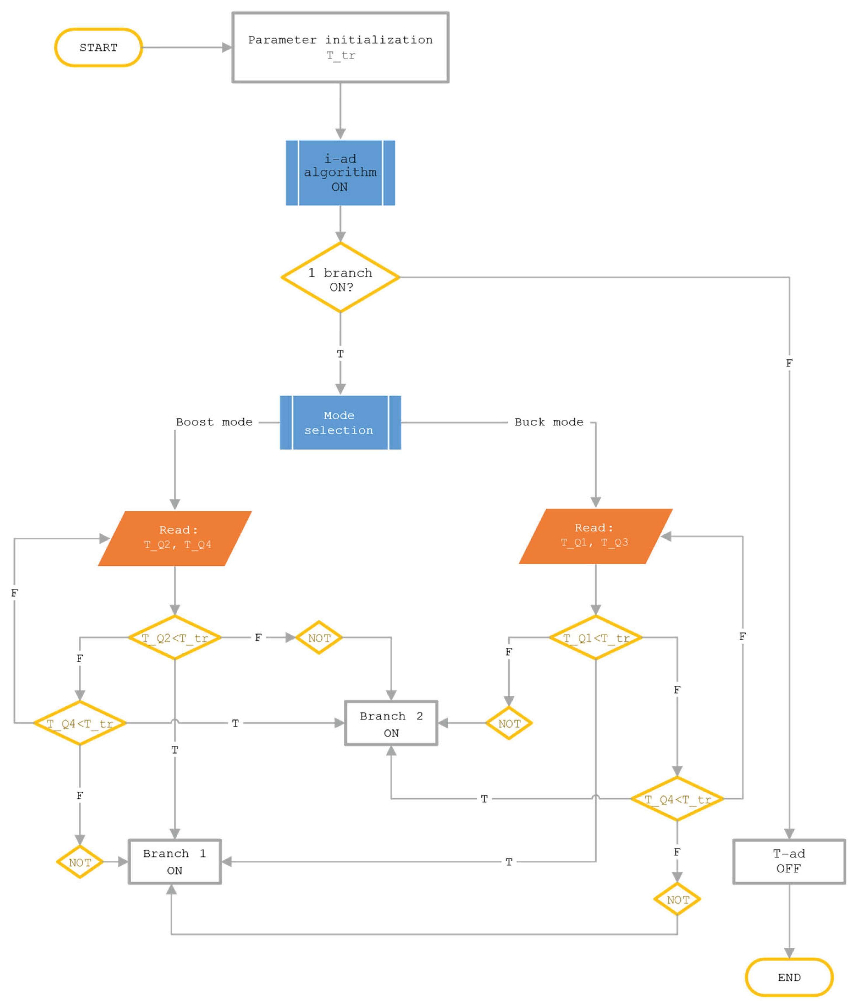
Figure 22.
Experimental setup used for CHIL-based validation of the combined current-adaptive and temperature-adaptive control algorithm.
Figure 22.
Experimental setup used for CHIL-based validation of the combined current-adaptive and temperature-adaptive control algorithm.
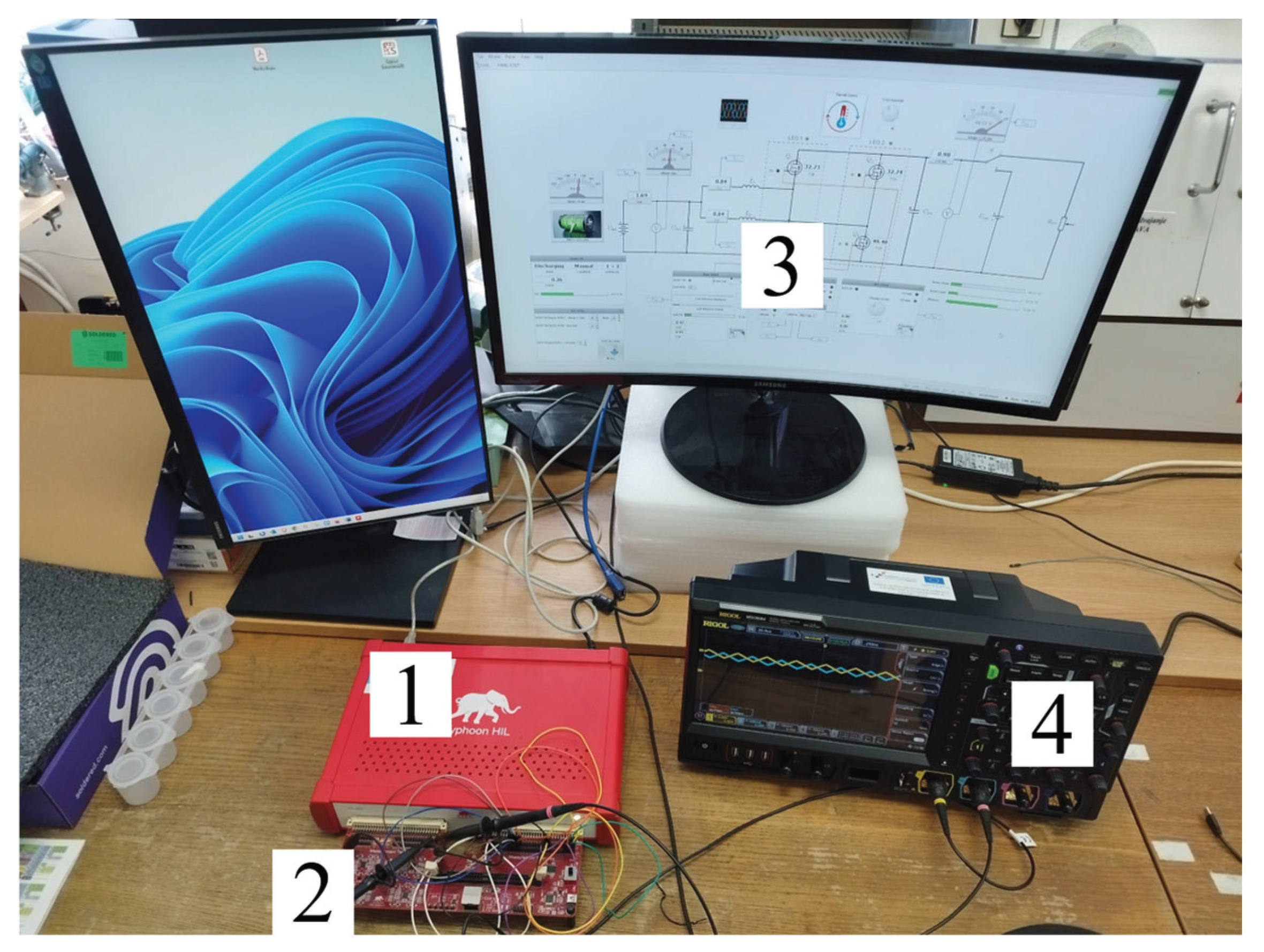
Figure 23.
Selected load profiles used in the experiments for (a) boost mode and (b) buck mode operation of the converter.
Figure 23.
Selected load profiles used in the experiments for (a) boost mode and (b) buck mode operation of the converter.
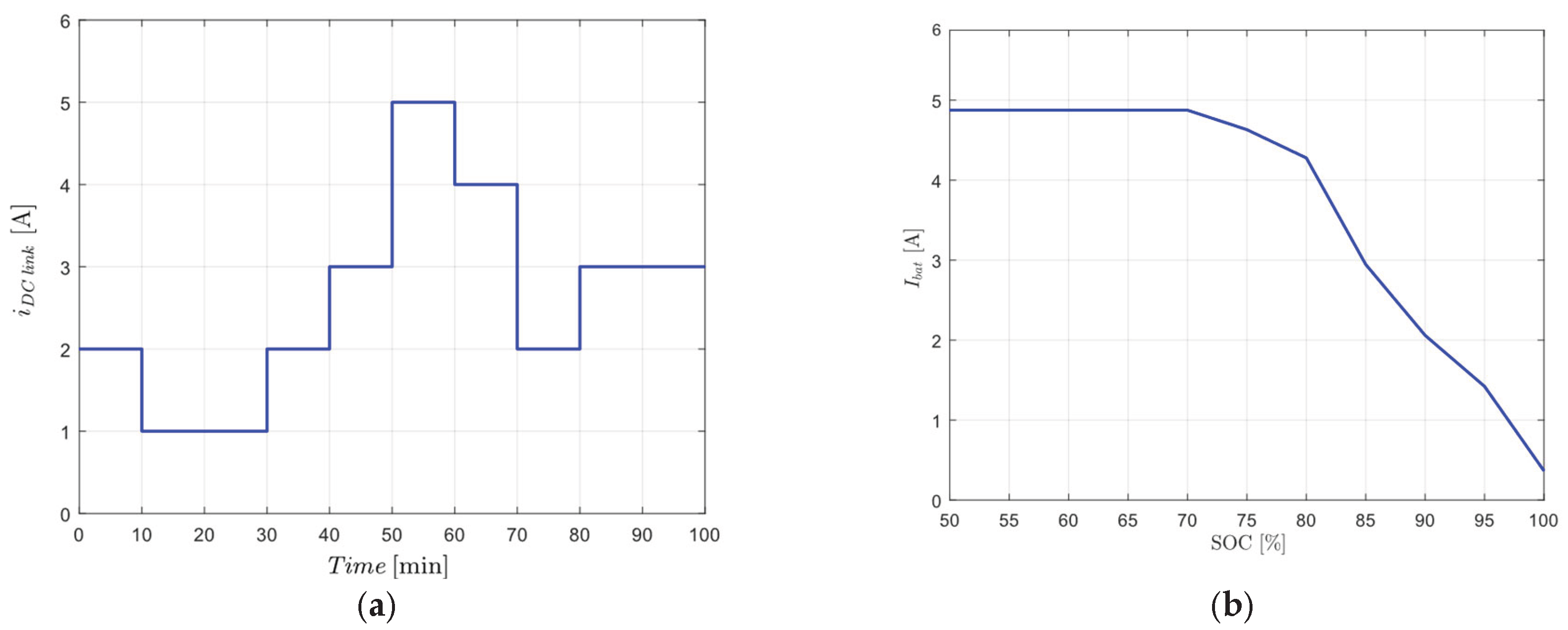
Figure 24.
Measurement results for the reference test set (Set 1), as defined in Table 5.
Figure 24.
Measurement results for the reference test set (Set 1), as defined in Table 5.
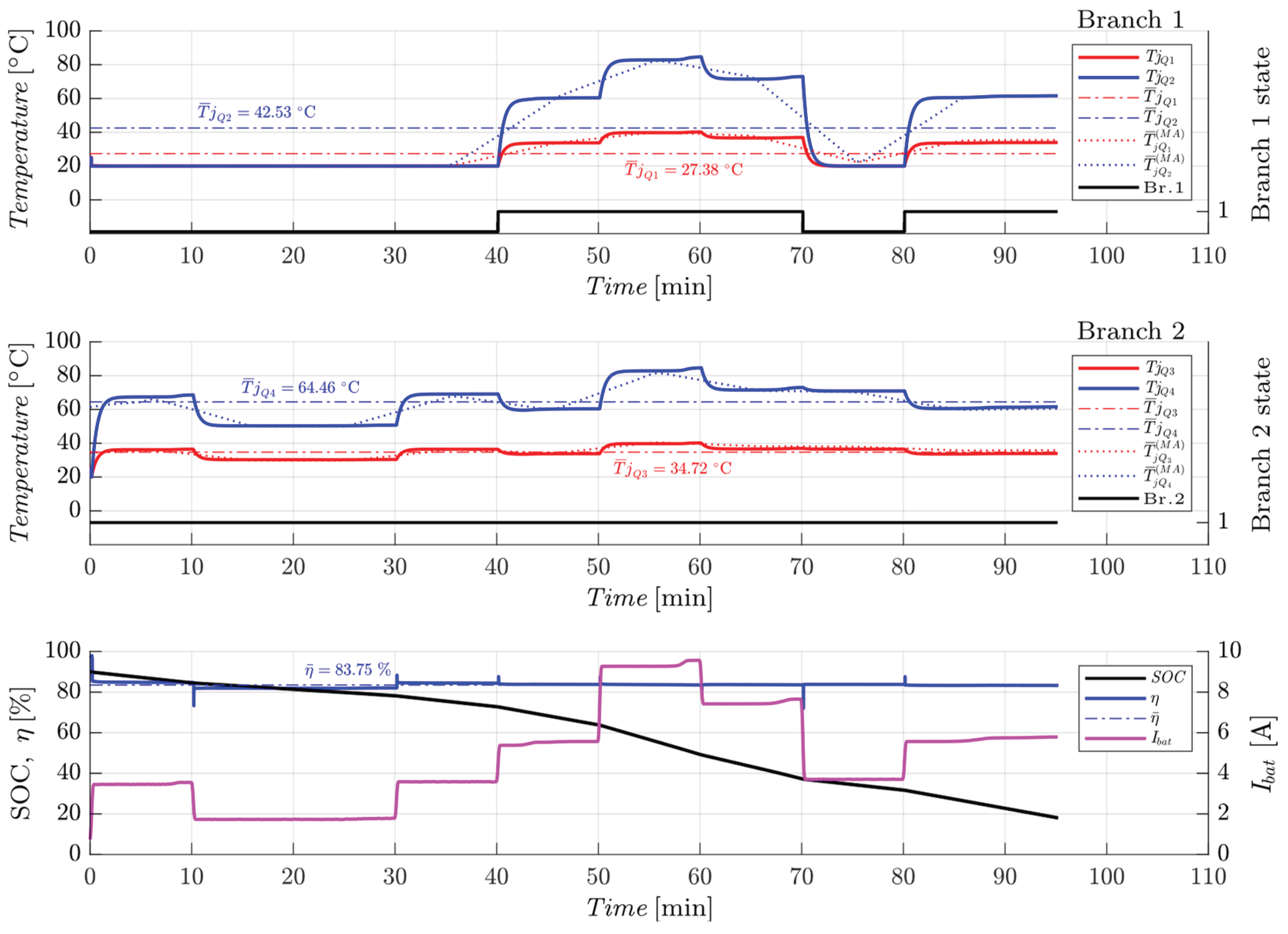
Figure 25.
Measurement results for Set 2 according to Table 5.
Figure 25.
Measurement results for Set 2 according to Table 5.
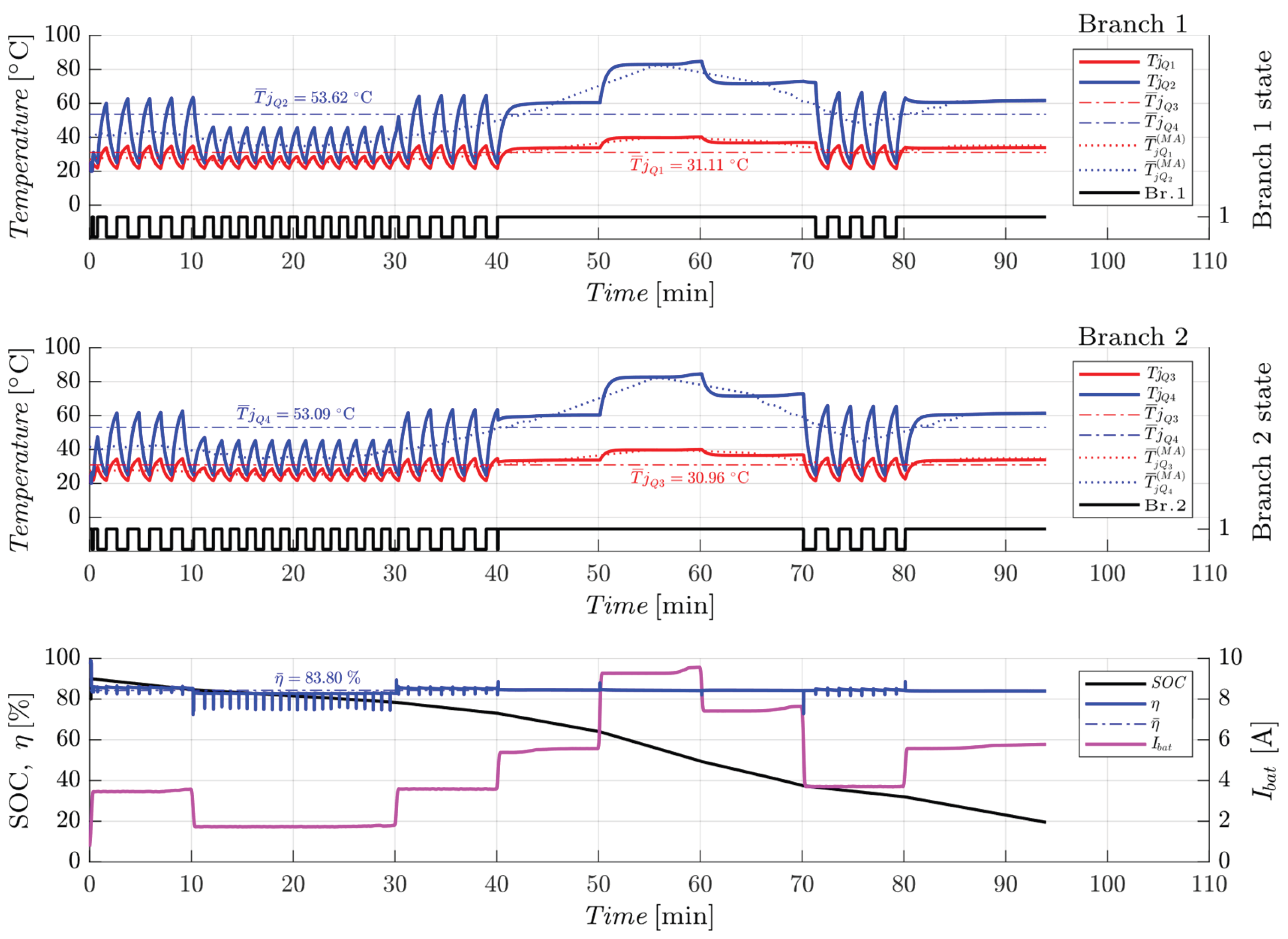
Figure 26.
Graphs of Measurement Results for Reference Set 3 According to Table 5.
Figure 26.
Graphs of Measurement Results for Reference Set 3 According to Table 5.
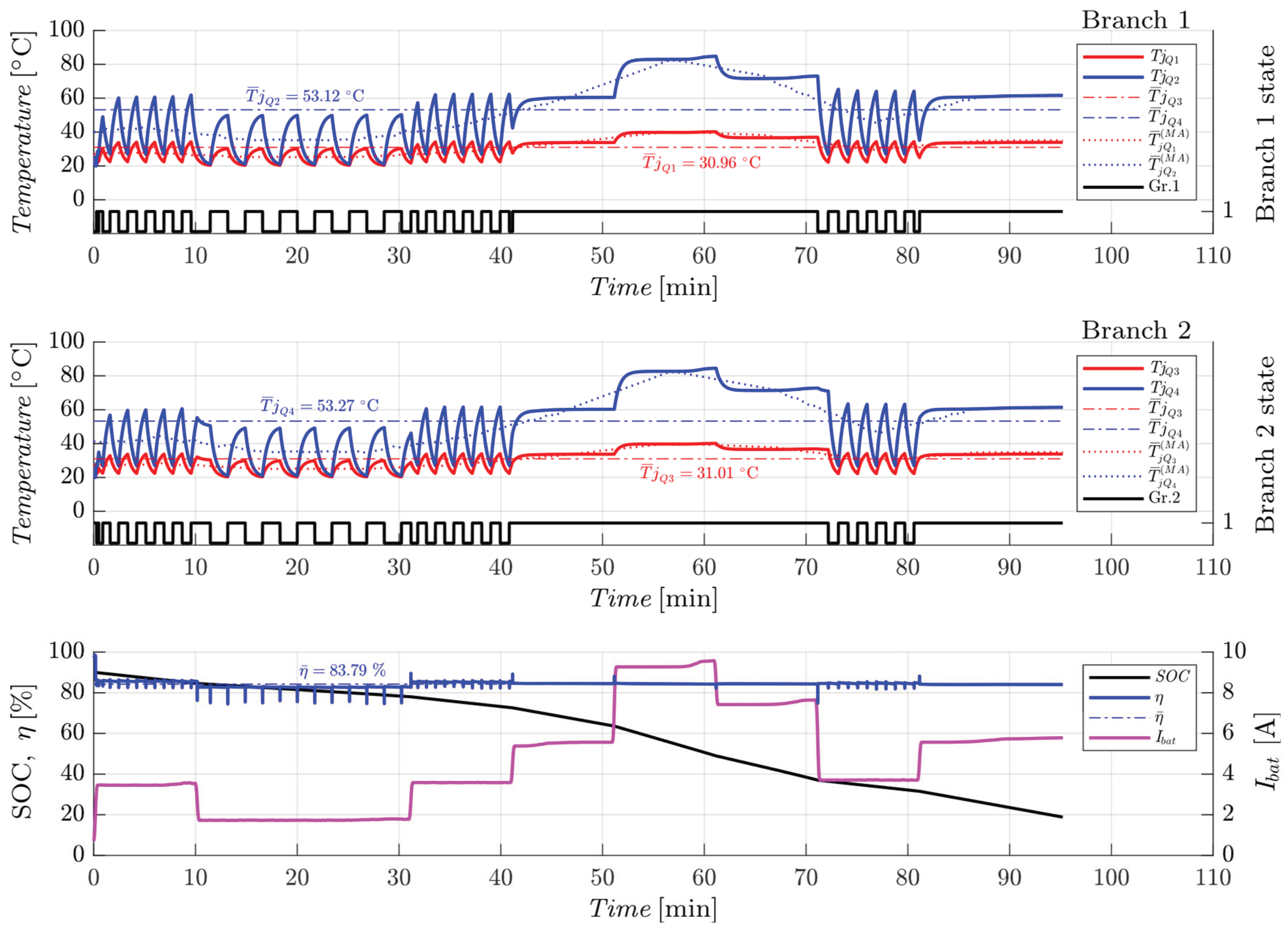
Figure 27.
Visual representation of key parameter trends during combined (current-adaptive and temperature-adaptive branch rotation) algorithm under boost mode operation.
Figure 27.
Visual representation of key parameter trends during combined (current-adaptive and temperature-adaptive branch rotation) algorithm under boost mode operation.
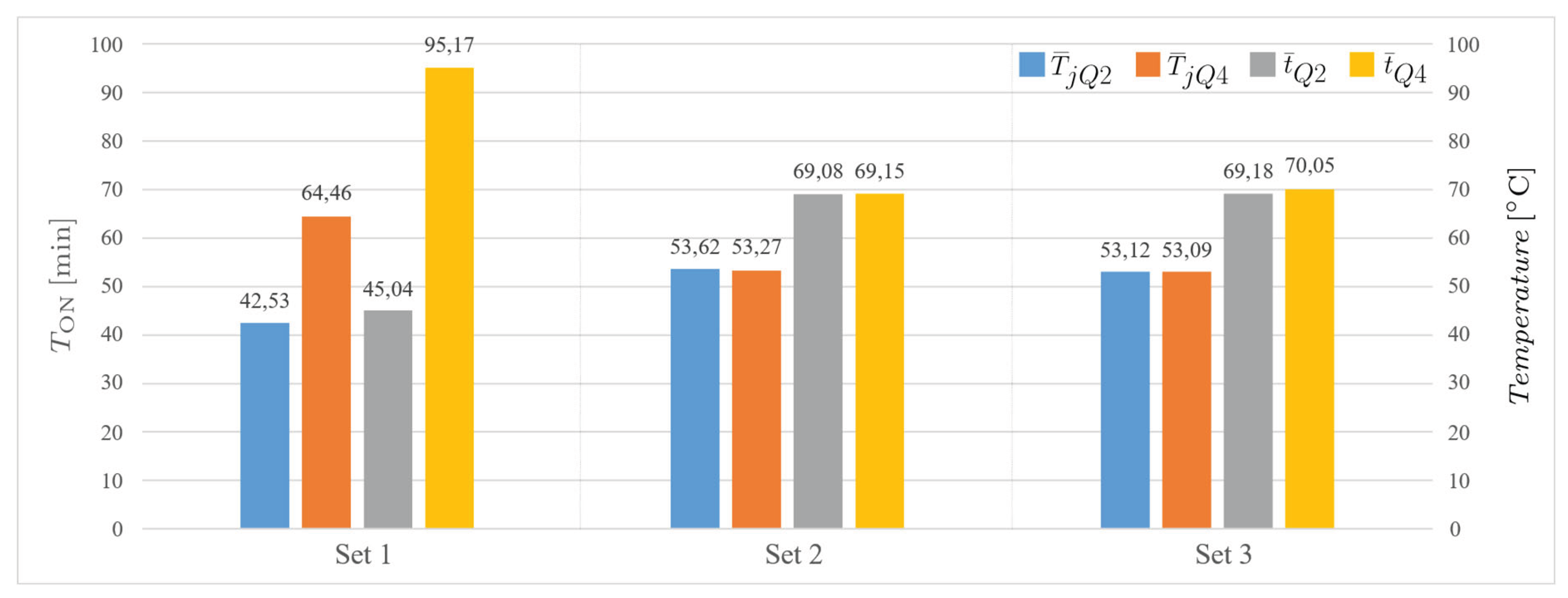
Figure 28.
Comparison between thermal (a) and electrical (b) time constants in the observed system.
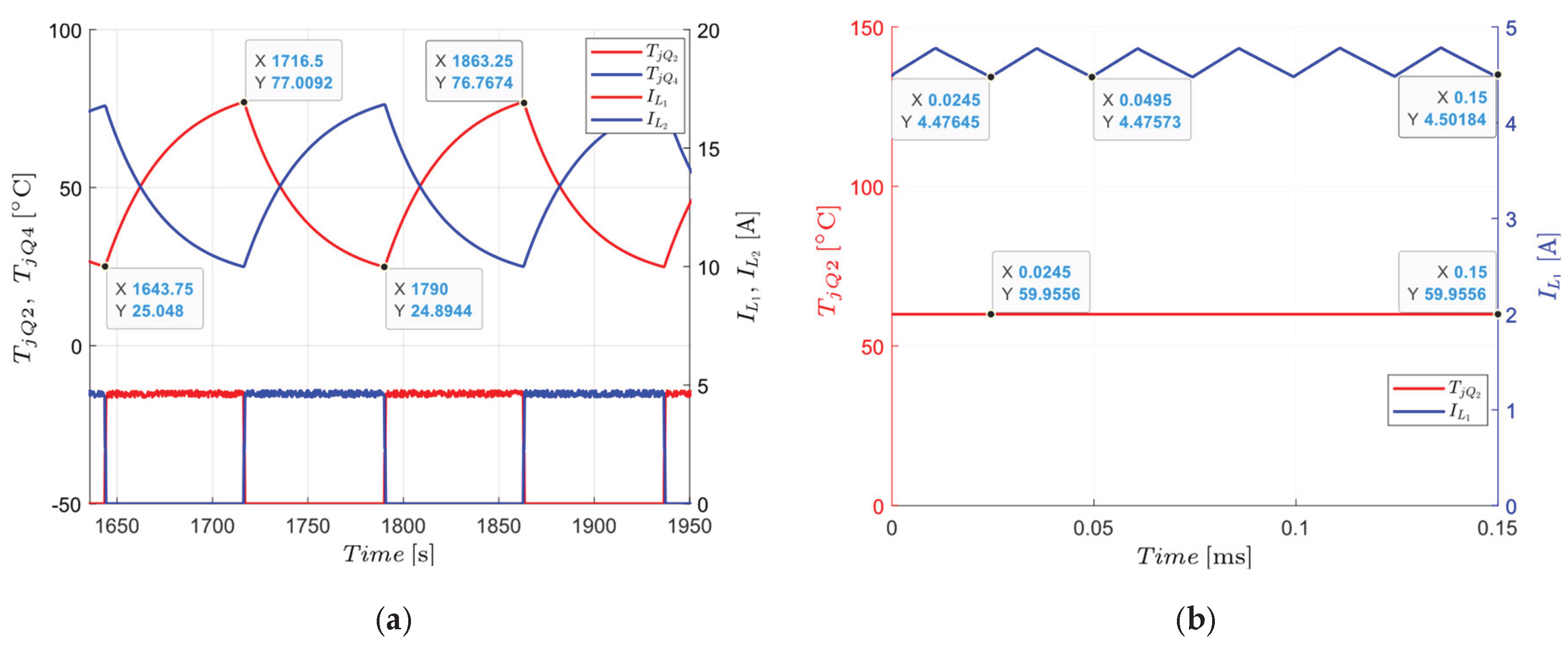
Figure 29.
Measurement results for the reference test set in buck mode operation (Set 4), according to Table 5.
Figure 29.
Measurement results for the reference test set in buck mode operation (Set 4), according to Table 5.
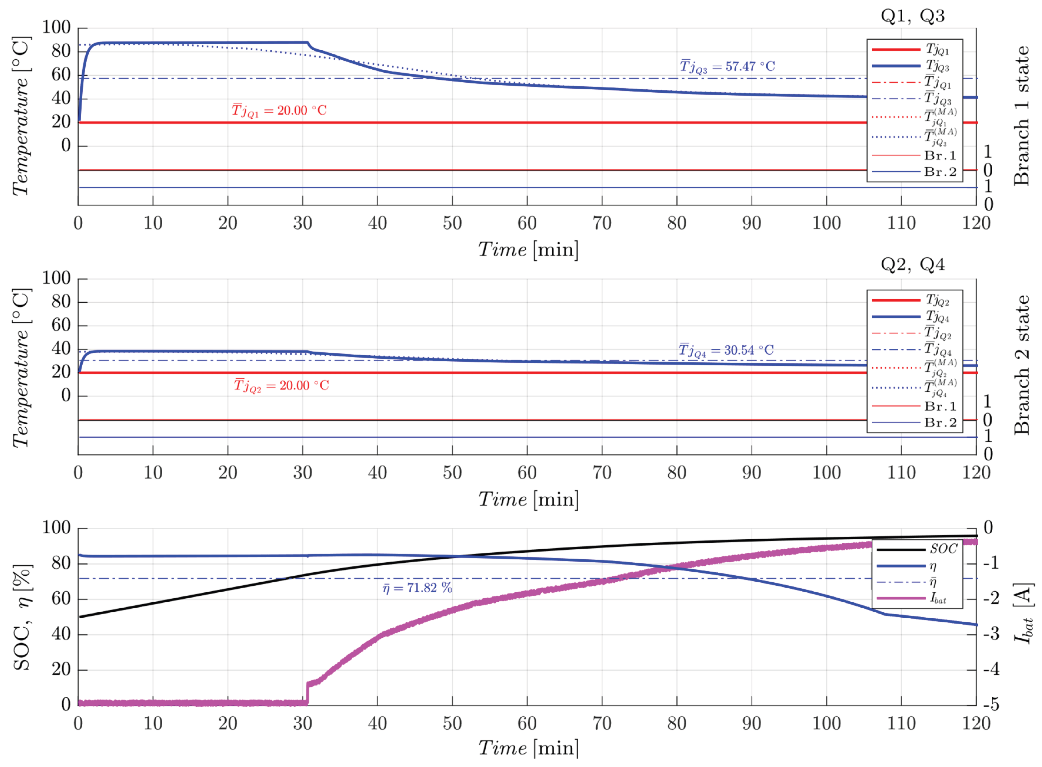
Figure 30.
Graphs of Measurement Results for Reference Set 5 According to Table 5.
Figure 30.
Graphs of Measurement Results for Reference Set 5 According to Table 5.
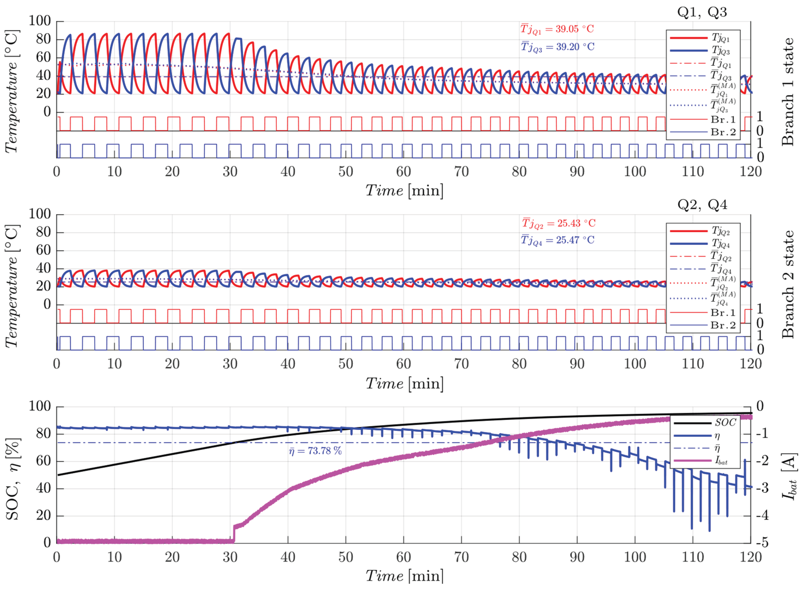
Table 1.
Configuration settings of the Typhoon HIL 402 system used in the Schematic Editor.
| Parameter | Value |
| Typhoon HIL 402 hardware configuration | |
| FPGA solver simulation step | |
| User microcontroller command execution interval |
|
| Number of used digital inputs/outputs | |
| Number of used analog outputs | |
| Number of used PWM modules | |
| Thermal model | Yes |
Table 2.
Selected basic parameters of the converter and BESS.
| Parameter | Symbol | Value |
| Number of converter branches | ||
| Maximum system power | ||
| Maximum power per branch | ||
| Converter switching frequency | ||
| Nominal DC-link voltage | ||
| Nominal battery voltage1 | ||
| Maximum battery current | ||
| Maximum current per single branch | ||
| Relative ripple of DC-link voltage | ||
| Relative ripple of battery voltage | ||
| Relative ripple of battery charging/discharging current |
1 Nominal battery pack voltage of 7S3P package is , while actual battery voltage varies.
Table 3.
Battery pack parameters.
| Category | Panasonic NCR18650B | 7S3Ppackage |
| Nominal battery voltage | ||
| Maximum battery voltage | ||
| Capacity | ||
| Standard charging current | ||
| Maximum discharging current | ||
| Monitoring | - | BMS |
Table 4.
Main System components on which simulation model from Figure 10 is based.
Table 4.
Main System components on which simulation model from Figure 10 is based.
| Component | Label (Fig. 11) | Manufacturer | Type | Main Electrical Characteristics |
| Inductor | API Delevan | PT1000-2050 | ; | |
| Capacitor | Vishay | 058/059 PLL-SI | ; | |
| 058/059 PLL-SI | ; | |||
| Transistor | STM | VNP10N07 | ; |
Table 5.
Validation test sets for the combined control algorithm using the CHIL methodology.
| Measurement set | 1 | 2 | 3 | 4 | 5 |
|---|---|---|---|---|---|
| Operating mode | Boost (discharging) | Buck (charging) | |||
| Current-adaptive operation | Automated | Automated | |||
| Branch rotation (temperature-adaptive operation) | OFF | ON | ON | OFF | ON |
| Temperature threshold | Variable |
||||
| Sampled variables | , , , , SOC , , | ||||
Table 6.
Processed measurement results for boost mode (Set 1 – Set 3), according to Table 5.
Table 6.
Processed measurement results for boost mode (Set 1 – Set 3), according to Table 5.
| Branch, transistor | Branch 1, | Branch 2, | |||
| Temperature parameter | |||||
| Set 1 (reference) | |||||
| Set 2 | |||||
| Set 3 | |||||
| Relative temperature difference between measurement sets | |||||
| Time related parameters | |||||
| Set 1 (reference) | |||||
| Set 2 | |||||
| Set 3 | |||||
Table 7.
Processed measurement results for buck mode operation (Sets 4–5), according to Table 5.
Table 7.
Processed measurement results for buck mode operation (Sets 4–5), according to Table 5.
| Branch, transistor | |||||
|---|---|---|---|---|---|
| Temperature parameter | |||||
| Set 4 (reference) | |||||
| Set 5 | |||||
| Relative temperature difference between measurement sets | |||||
| Time related parameters | |||||
| Set 4 (reference) | |||||
| Set 5 | |||||
Disclaimer/Publisher’s Note: The statements, opinions and data contained in all publications are solely those of the individual author(s) and contributor(s) and not of MDPI and/or the editor(s). MDPI and/or the editor(s) disclaim responsibility for any injury to people or property resulting from any ideas, methods, instructions or products referred to in the content. |
© 2026 by the authors. Licensee MDPI, Basel, Switzerland. This article is an open access article distributed under the terms and conditions of the Creative Commons Attribution (CC BY) license (http://creativecommons.org/licenses/by/4.0/).
Copyright: This open access article is published under a Creative Commons CC BY 4.0 license, which permit the free download, distribution, and reuse, provided that the author and preprint are cited in any reuse.


