Submitted:
23 January 2026
Posted:
26 January 2026
You are already at the latest version
Abstract
Reconfigurable logic is crucial for future adaptive computing but are challenging to realize with conventional complementary metal-oxide-semiconductor technology due to the limited field-effect characteristics of the fundamental silicon devices. Two-dimensional materials offer a promising platform, yet enhancing their functional versatility requires novel operational mechanisms. Here, we demonstrate a single WSe₂/h-BN/graphene heterojunction capable of dynamically switching between distinct logic functions—XNOR and IMP—simply by modulating the drain-source voltage. At a low bias of 0.3 V, the carrier distribution is governed by capacitive coupling, realizing an XNOR gate. Increasing the bias to 3 V activates Fowler–Nordheim tunneling between the graphene floating gate and the drain, enabling IMP logic operation. The interplay and voltage-induced transition between these two physical mechanisms underpins the device's multifunctional capability. This work introduces a novel operational strategy for two-dimensional material-based reconfigurable logic, providing a pathway toward compact, adaptive hardware for post-CMOS computing.
Keywords:
reconfigurable logic
; electrically tunable
; Fowler-Nordheim tunnel
1. Introduction
The miniaturization of conventional metal-oxide-semiconductor field-effect transistors (MOSFETs) is approaching its physical limits.[1] To further improve information processing performances, electronic devices based on new physical principles or emerging technologies are required.[2,3,4] In this context, reconfigurable logic has emerged as a transformative paradigm, offering the ability to dynamically alter circuit functionality within the same hardware footprint.[5,6,7,8,9,10]Such capability is crucial for adapting to diverse computational tasks, enhancing hardware utilization, and enabling more flexible and compact computing systems, which are central to the development of adaptive electronics, edge computing, and neuromorphic engineering.[11,12]
The advent of two-dimensional (2D) materials has opened new avenues for such innovations.[10] Materials like graphene, transition metal dichalcogenides, and hexagonal boron nitride exhibit exceptional electronic, optical, and mechanical properties, along with atomically thin bodies that enable potent electrostatic control.[13,14,15,16,17] Over the past decade, researches into 2D material-based transistors and logic devices have intensified, demonstrating promising pathway toward more sophisticated, functionally integrated systems.[9,11,18,19,20,21,22,23,24]Notably, these include the development of neuromorphic computing components that mimic synaptic and neuronal functions for energy-efficient, brain-inspired hardware;[8,25,26] devices capable of synergistic optoelectronic co-modulation, where optical and electrical inputs interact to define novel operational states;[18,27,28,29,30,31,32] and architectures that integrate logic and non-volatile memory functions (logic-in-memory)—to overcome the von Neumann bottleneck. [33,34,35]Collectively, these advances underscore a shift from simple electronic switches toward reconfigurable, multi-domain systems with broader application potential. Despite these advances, the versatility of 2D logic devices can be further enhanced by introducing novel operational mechanisms, thereby enabling distinct reconfigurable logic from a single device.
Here, we demonstrate a WSe₂/h-BN/graphene heterostructure that exhibits dynamically reconfigurable multifunctional logic operations (XNOR and IMP), controlled by the polarity combinations of gates and drain voltages. The ambipolar WSe₂ channel is simultaneously modulated by the floating gate and the back gate, where the floating-gate voltage regulates the channel regions on both sides of the electrode, while the back-gate voltage governs the central area of the channel. Under a low source-drain bias (0.3 V), the electrostatic coupling from both the floating gate and the back gate primarily dictates the carrier distribution within the channel, enabling the realization of XNOR logic function. When the source-drain bias is increased (3 V), the operational mechanism moves beyond the established paradigm of capacitive coupling and Fowler–Nordheim tunneling between the floating gate and the drain emerges as an essential and complementary switching mechanism, which allows the device to perform IMP logic. The co-existence and interplay of these two mechanisms underpin the device’s multifunctional capability. By introducing a new mechanistic dimension into 2D device operation, this work provides a viable pathway toward more versatile and compact post-CMOS computing hardware.
2. Materials and Methods
A schematic diagram of the heterojunction fabricated on a commercial silicon-on-insulator (SOI) wafer is depicted in Figure 1a, where tungsten diselenide (WSe2), hexagonal boron nitride (h-BN), and graphene (Gr) flakes serve as the channel layer, tunneling dielectric, and floating gate, respectively. Two graphene floating gates (FG) are placed beneath the source and drain electrodes, respectively, and connected together to serve as input 1 (IN1), with the heavily doped silicon back gate (BG) acting as the input 2 (IN2). Figure 1b shows the optical microscope image of the photodetector, where WSe2, h-BN, and Gr flakes are indicated by blue, green, and purple dashed lines, respectively. As shown in the figure, the channel length between the source and drain is approximately 6.5 μm. The Raman spectroscopy of the Gr flakes, h-BN flakes, h-BN/Gr heterostructure, and WSe2/h-BN/Gr heterostructure are depicted in Figure 1c. The WSe2 flakes exhibit one characteristic peak at 254 cm−1, corresponding to the out-of-plane (A1g) vibrational modes. The characteristic peak of h-BN is located at 1366 cm−1, corresponding to the in-plane (E2g) vibrational mode. Furthermore, the peaks at 1578 cm−1 (G) and 2705 cm−1 (2D) are two typical characteristic peaks of multi-layer graphene. The cross-sectional TEM image and energy-dispersive spectrometry (EDS) of WSe2/h-BN/Gr heterostructure beneath the source electrode is obtained and the results are shown in Figure 1d. The boundary of h-BN/Gr and WSe2/h-BN interfaces can be clearly resolved, and the thicknesses of WSe2, h-BN, and Gr flakes is identified to be 1.1, 11.5 and 1.5 nm, respectively, in good accordance with the atomic force microscopy (AFM) results in Figure 1e.
The heterostructure was constructed with standard dry transfer method. The commercial SiO₂/Si substrate (285 nm oxide thickness) first underwent a standard cleaning procedure. It was immersed sequentially in acetone, isopropanol (IPA), and deionized (DI) water, followed by drying with a nitrogen stream to obtain an atomically clean surface. Subsequently, flakes of multilayer graphene, h-BN, and WSe₂ were transferred onto the pre-cleaned SiO₂ surface via mechanical exfoliation. The PC adhesion layer can pick up 2D materials at ~90 ℃ and release at ~180 ℃ and the WSe2, h-BN flakes were sequentially picked up by this polymer and finally released onto the graphene flake on the SiO2/Si substrate.[36] The remaining polycarbonate (PC) was dissolved in a chloroform (CHCl₃) bath for two minutes. Subsequently, the device was annealed at 300 °C under vacuum for three hours to improve interfacial contact and release residual stress within the heterostructure. Finally, electrodes were defined via standard electron-beam lithography (EBL) and deposited by electron-beam evaporation of Cr/Au (5/50 nm).
3. Results and Discussions
The electrical properties of WSe2 layer were firstly characterized by I-V and transfer curve measurements. Figure 2a presents the I-V characteristics of WSe2/h-BN/Gr heterostructure under various floating-gate voltages. (Schematic of the measurement circuit for Figure 2a-c is illustrated in Figure S1.) The curves maintain a linear relationship even with increasing gate bias, indicating excellent ohmic contact between the two-dimensional (2D) materials and the electrodes. Figure 2b shows the transfer curve of WSe2 at a source-drain voltage of 0.3 V under floating-gate modulation. The curve exhibits ambipolar behavior with a high on/off ratio of up to 106, demonstrating effective control of WSe2 by the floating gate. Figure 2c shows the transfer curve of WSe2 under back-gate modulation and the curve exhibits a clear hysteresis window resulting from the charge trapping and release in the floating gate.[37,38] Overall, the WSe₂ demonstrates effective and independent modulation by both the floating gate and the back gate. Besides, the WSe₂ channel exhibits clear ambipolar conduction and the maximum on-state current occurs at a floating-gate voltage of 8 V (back-gate voltage of 30 V) for electron-dominated conduction and -8 V (back-gate voltage of -60 V) for hole-dominated conduction.
As shown in Figure 1a, the device’s channel is electrostatically controlled by both the floating gate and the back gate, with the FG dominating near the electric contacts and the BG in the mid-channel. High conduction is achieved only when both gates accumulate carriers of the same type (both electrons or holes). When both gates bias the channel toward electron/hole accumulation, a uniform conductive path forms, turning the device on. Conversely, a mismatch in carrier type—where one gate induces electron conduction and the other induces hole conduction—creates a potential barrier or carrier depletion in the channel, thus leading to a significantly reduced drain current. Figure 2d,g present the I-V characteristics measured at a floating-gate voltage of 8 V/-8 V, with the back-gate voltage set to 30 V and -60 V. Similarly, Figure 2e,h demonstrate the I-V characteristics under a constant BG voltage of 30 V (-60 V), with the FG voltage set to 8 V and -8 V. A key observation from the figures is that the channel current is significantly larger when the floating-gate and back-gate voltages have the same polarity, compared to when they have opposite polarities. The source-drain current with VFG = 8 V (-8 V) and VBG = 30 V (-60 V) is substantially higher than that with VFG = 8 V (-8 V) and VBG = -60 V (30 V), highlighting the critical role of gate voltage alignment.
Furthermore, the drain current increases with the applied source-drain voltage, as expected. Figure 2f,i present the corresponding transfer curves measured at source-drain voltages of 0.3 V and 3 V, respectively. At VD = 0.3 V, the transfer curve exhibits n-type semiconductor behavior when VBG = 30 V, while exhibits p-type behavior when VBG = -60 V. This indicates that back-gate voltage determines the type of majority carrier induced in the channel layer. By applying floating-gate voltage and back-gate voltage as inputs, the device can be configured to function as a XNOR logic gate. In contrast, at VD = 3 V, a distinct ambipolar behavior is observed in the transfer characteristics when VBG = 30 V, while the transfer curve maintains p-type behavior when VBG = -60 V. The underlying mechanism for this ambipolar behavior is the strengthening electric field between the floating gate and the drain with increasing drain bias. This enhanced field gives electrons a higher probability of tunneling from the floating gate to the drain, thereby inducing n-type characteristics in the channel region near the drain, similar to the central region.[39] By utilizing the electron tunneling effect, the device can be configured to function as IMP logic gate, with floating-gate voltage and back-gate voltage as inputs.
To elucidate the reconfigurable logic functionality of the device, we investigate its operating mechanism by examining the charge carrier distribution and energy band structure. The charge carrier distribution through the WSe₂ channel is jointly modulated by the silicon back gate (VBG), the graphene floating gate (VFG), and the drain-source bias (VD). We take the device under a small VD (0.3 V) as a detailed example to illustrate how floating-gate voltage (IN1) and back-gate voltage (IN2) affect the charge carrier distribution. As shown in Figure 3a, When the VFG and VBG are set to -8 V and -60 V ((IN1,IN2) = (-8 V,-60 V)), a negative voltage applied to the floating gate induces hole accumulation in the channel regions near the source and drain electrodes due to electrostatic induction. Similarly, a negative voltage applied to the back gate leads to hole accumulation in the central region of the channel. (Due to electrostatic screening from the floating gate, the back-gate capacitive coupling effect is largely restricted to the central part of the channel.) Consequently, the entire channel exhibits p-type conduction behavior. Conversely, when the VFG and VBG are set to -8 V and 30 V ((IN1,IN2) = (-8 V,30 V)), the negative floating-gate voltage still causes hole accumulation near the electrodes, while the positive back-gate voltage induces electron accumulation in the middle section of the channel. This results in a p-n-p configuration across the channel. The formation of the central electron-potential well significantly suppresses the source-drain current. The charge distributions for the remaining cases, derived from the same analysis, are also presented in the figure. The results demonstrate that the channel conduction is uniformly n-type (when (IN1,IN2) = (8 V,30 V)) or p-type (when (IN1,IN2) = (-8 V,-60 V)) when the floating-gate and back-gate voltages share the same-polarity, whereas opposite polarities induce either an electron ((IN1,IN2) = (-8 V,30 V)) or hole ((IN1,IN2) = (8 V,-60 V))potential well, leading to a significantly suppressed source-drain current. This observation is fully consistent with the transport properties presented earlier.
When the drain-source voltage is set to 3 V (Figure 3b), the device behavior differs under a floating-gate voltage of -8 V. At VD = 3 V and VFG = -8 V, the electric field across h-BN becomes sufficiently strong to induce tunneling. Consequently, the floating gate modulates the channel carrier distribution predominantly through direct charge injection instead of capacitive coupling. Figure 3c presents the energy band diagrams of the device under a source-drain voltage of 3 V and a floating-gate voltage of -8 V, with the back-gate voltage set to -60 V and 30 V, respectively. A back-gate voltage of -60 V generates a stronger electric field in h-BN tunneling layer, leading to more pronounced band bending. This stronger band bending facilitates greater electron tunneling into the channel. In contrast, at VBG = 30 V, the electric field induced by the back gate in h-BN opposes that of the floating gate, thereby partially canceling the overall field and resulting in weaker band bending and thus less electron tunneling. The corresponding tunneling currents are quantified in Figure 3d measured at VFG = -8 V for VBG = 30 V/-60 V. It is evident that the tunneling current at VBG = -60 V is significantly larger than that for VBG = 30 V. This experimental result directly corroborates the theoretical analysis presented above.
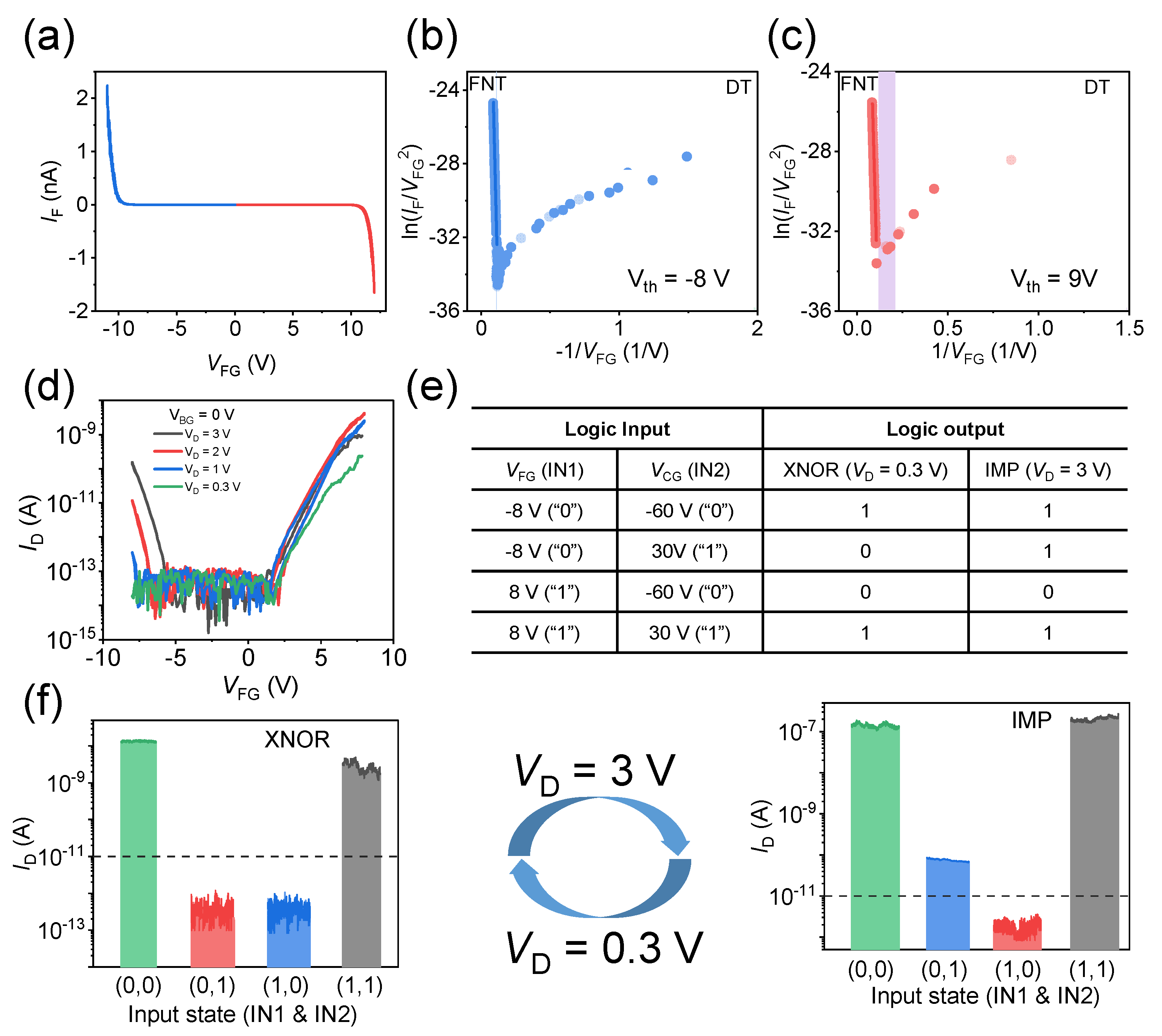
To gain deeper insight into the mechanism of electron tunneling, Figure 4a presents the tunneling current versus voltage characteristics for WSe2/h-BN/Gr heterostructure, with the corresponding test setup shown in Figure S2. As observed, the tunneling current remains low at small floating-gate voltages. When the voltage exceeds a certain threshold, the current exhibits a sharp exponential increase. This behavior is attributed to a transition in the tunneling mechanism: direct tunneling (DT) dominates at lower voltages, while Fowler-Nordheim tunneling (FNT) becomes operative above the threshold voltage. The relationship between current density (J) and electric field (E) for direct tunneling and FN tunneling are given below:
where A and B are constants.[40,41] It can be derived from the equations that for direct tunneling: and for Fowler-Nordheim tunneling: . Figure 4b,c presents the plots of versus for backward and forward sweeps of the floating-gate voltage. Figure S3 presents the plots of versus for backward and forward sweeps of the floating-gate voltage. From these curves, the threshold voltages for FNT are extracted to be approximately 9 V (forward sweep) and -8 V (reverse sweep), respectively. This asymmetry stems from the difference in the energy barriers that carriers must overcome: during the forward sweep, the primary barrier is at the Gr/h-BN interface, whereas during the reverse sweep, it is at the WSe2/h-BN interface. The distinct heights of these two interfaces account for the observed difference in threshold voltages. Since a lower threshold voltage is required for tunneling in the negative FG direction, our work employs a drain voltage of 3 V combined with an FG voltage of -8 V to implement the IMP logic function, rather than using a drain voltage of -3 V with an FG voltage of 8 V.
Figure 4d shows the source-drain current as a function of the FG voltage under different source-drain biases, with the back gate grounded. It clearly demonstrates that a higher VD lowers the FG voltage needed to trigger FNT. Notably, the current remains minimal before FNT occurs, because the capacitive coupling effect dominates at the carrier redistribution process. By exploiting the transition of the dominant operating mechanism between capacitive coupling and electron tunneling, the reconfigurable logic functions of XNOR and IMP are achieved and the corresponding truth table is presented in Figure 4e. Here, −8 V and 8 V are used to represent the logic 0 and 1 for IN1 and −60 V and 30 V are used to represent the logic 0 and 1 for IN2. The logic output is defined by the channel current and a logic output of “1” is defined as a current greater than 10-11 A, while a logic “0” corresponds to a current less than 10-11 A. Figure 4f displays the output currents measured under different combinations of input logic for XNOR and IMP logic. As can be seen from the figure, the device operates as a XNOR logic gate at VD = 0.3 V, and as a IMP logic gate at VD = 3 V. Therefore, the logic function can be switched simply by adjusting the source-drain voltage.
4. Conclusions
In summary, we have demonstrated a dynamically reconfigurable logic device based on WSe2/h-BN/Gr heterostructure. The carrier distribution in the bipolar WSe₂ channel is simultaneously controlled by the floating-gate voltage, back-gate voltage and the source-drain voltage, where the floating-gate voltage regulates the channel regions on both sides of the electrode, while the back-gate voltage governs the central area of the channel. Under a small source-drain voltage, the channel carrier distribution is primarily governed by electrostatic modulation induced by the floating gate and the back gate, thereby achieving XNOR logic. As the source-drain voltage increases, Fowler-Nordheim tunneling between the floating gate and the drain electrode, coupled with significant capacitive coupling, becomes the dominant operational mechanism, enabling the device to execute IMP logic. The developed two-dimensional reconfigurable heterojunction offers a promising pathway toward compact, multi-functional logic elements with simplified operational control, providing a tangible advantage for future adaptive electronic systems.
Supplementary Materials
The following supporting information can be downloaded at: Preprints.org.
Author Contributions
Conceptualization, Y.H.; methodology, Y.H.; investigation, Y.H.; resources, Z.Z.; data curation, Y.H.; writing—original draft preparation, Y.H.; writing—review and editing, Y.H. and Z.Z; visualization, Y.H.; supervision, Z.Z.; project administration, Z.Z.; funding acquisition, Z.Z. All authors have read and agreed to the published version of the manuscript.
Funding
This work was financially supported by the National Natural Science Foundation of China (no. 62204262).
Acknowledgments
We thank Mr. Xin Zhang and Mr. WeiBin Wu from the Analytical Instrumentation Center of Hunan University for their assistance with HRSTEM and FIB experiments.
Conflicts of Interest
The authors declare no conflicts of interest.
References
- Qiu, C., et al., Dirac-source field-effect transistors as energy-efficient, high-performance electronic switches. Science, 2018. 361(6400): p. 387-392.
- Gaillardon, P.-E., et al., A Novel FPGA Architecture Based on Ultrafine Grain Reconfigurable Logic Cells. IEEE Transactions on Very Large Scale Integration (VLSI) Systems, 2015. 23(10): p. 2187-2197.
- Huang, M., et al., Multifunctional high-performance van der Waals heterostructures. Nature Nanotechnology, 2017. 12(12): p. 1148-1154.
- Orji, N.G., et al., Metrology for the next generation of semiconductor devices. Nature Electronics, 2018. 1(10): p. 532-547.
- Liu, Y., et al., Ambipolar Barristors for Reconfigurable Logic Circuits. Nano Lett, 2017. 17(3): p. 1448-1454.
- Liu, C., et al., Small footprint transistor architecture for photoswitching logic and in situ memory. Nat Nanotechnol, 2019. 14(7): p. 662-667.
- Cheng, R., et al., High-performance, multifunctional devices based on asymmetric van der Waals heterostructures. Nature Electronics, 2018. 1(6): p. 356-361.
- Pan, C., Wang, CY., Liang, SJ. et al. Reconfigurable logic and neuromorphic circuits based on electrically tunable two-dimensional homojunctions. Nat Electron 3, 383–390 (2020).
- Hou, X., et al., A Logic-Memory Transistor with the Integration of Visible Information Sensing-Memory-Processing. Advanced Science, 2020. 7(21).
- Migliato Marega, G., et al., Logic-in-memory based on an atomically thin semiconductor. Nature, 2020. 587(7832): p. 72-77.
- Wu, P., et al., Two-dimensional transistors with reconfigurable polarities for secure circuits. Nature Electronics, 2020. 4(1): p. 45-53.
- Xiong, X., et al., Reconfigurable Logic-in-Memory and Multilingual Artificial Synapses Based on 2D Heterostructures. Advanced Functional Materials, 2020. 30(11).
- Geim, A.K. and I.V. Grigorieva, Van der Waals heterostructures. Nature, 2013. 499(7459): p. 419-25.
- Novoselov, K.S., et al., 2D materials and van der Waals heterostructures. Science, 2016. 353(6298): p. aac9439.
- Tan, C., et al., Recent Advances in Ultrathin Two-Dimensional Nanomaterials. Chem Rev, 2017. 117(9): p. 6225-6331.
- Massicotte, M., Schmidt, P., Vialla, F. et al. Picosecond photoresponse in van der Waals heterostructures. Nature Nanotech 11, 42–46 (2016).
- Zhao, S., Y. Cheng, and L. Tao, Modulation and Optoelectronic Applications of van der Waals Interlayer Excitons. ACS Photonics, 2024. 11(7): p. 2529-2545.
- Zhu, T., et al., Gate Voltage- and Bias Voltage-Tunable Staggered-Gap to Broken-Gap Transition Based on WSe2/Ta2NiSe5 Heterostructure for Multimode Optoelectronic Logic Gate. ACS Nano, 2024. 18(17): p. 11462-11473.
- Zhao, Z., et al., Content-Addressable Memories and Transformable Logic Circuits Based on Ferroelectric Reconfigurable Transistors for In-Memory Computing. ACS Nano, 2024. 18(4): p. 2763-2771.
- Zhao, R., et al., Reconfigurable aJ-Level Ferroelectric Transistor-Based Boolean Logic for Logic-in-Memory. Nano Letters, 2024. 24(35): p. 10957-10963.
- Chen, B., et al., Reconfigurable memlogic long wave infrared sensing with superconductors. Light: Science & Applications, 2024. 13(1).
- Ram, A., et al., Reconfigurable Multifunctional van der Waals Ferroelectric Devices and Logic Circuits. ACS Nano, 2023. 17(21): p. 21865-21877.
- Sheng Z, Dong J, Hu W, Wang Y, Sun H, Zhang DW, Zhou P, Zhang Z. Reconfigurable Logic-in-Memory Computing Based on a Polarity-Controllable Two-Dimensional Transistor. Nano Lett. 2023 Jun 14;23(11):5242-5249.
- Lee, C.J., et al., Two-Terminal Self-Gating Random-Access Memory Based on Partially Aligned 2D Heterostructures. Advanced Electronic Materials, 2022. 8(10).
- Liu, G., et al., Multifunctional Multigate One-Transistor with Thin Advanced Materials, Logic-in-Memory, and Artificial Synaptic Behaviors. ACS Applied Materials & Interfaces, 2023. 15(48): p. 55957-55964.
- Liu, T., et al., Hardware Efficient Reconfigurable Logic-in-Memory Circuit Based Neural Network Computing, in 2023 IEEE International Symposium on Circuits and Systems (ISCAS). 2023. p. 1-5.
- Jiazila, N., et al., Programmable WSe2 2D Lateral p-n Junctions Controlled by Dual Floating Gates. Advanced Functional Materials, 2025. 35(27).
- Tsai, M.-Y., et al., A reconfigurable transistor and memory based on a two-dimensional heterostructure and photoinduced trapping. Nature Electronics, 2023. 6(10): p. 755-764.
- Li, K., et al., Light-Triggered and Polarity-Switchable Homojunctions for Optoelectronic Logic Devices. Advanced Optical Materials, 2023. 11(7).
- Yang, Q., et al., Controlled Optoelectronic Response in van der Waals Heterostructures for In-Sensor Computing. Advanced Functional Materials, 2022. 32.
- Wang, S., et al., Nonvolatile van der Waals Heterostructure Phototransistor for Encrypted Optoelectronic Logic Circuit. ACS Nano, 2022. 16(3): p. 4528-4535.
- Zhang, K., et al., Photon-Memristive System for Logic Calculation and Nonvolatile Photonic Storage. Advanced Functional Materials, 2020. 30(34).
- Reis, D., Reconfigurable logic-in-memory. Nature Electronics, 2022. 5(11): p. 713-714.
- Kim, S., et al., Investigation on floating-gate field-effect transistor for logic-in-memory application. Journal of Physics D: Applied Physics, 2023. 56(49).
- Peng, R., et al., Programmable graded doping for reconfigurable molybdenum ditelluride devices. Nature Electronics, 2023. 6(11): p. 852-861.
- Wakafuji, Y., et al., 3D Manipulation of 2D Materials Using Microdome Polymer. Nano Lett, 2020. 20(4): p. 2486-2492.
- Sasaki, T., et al., Understanding the Memory Window Overestimation of 2D Materials Based Floating Gate Type Memory Devices by Measuring Floating Gate Voltage. Small, 2020. 16(47).
- Liu, L., et al., Ultrafast non-volatile flash memory based on van der Waals heterostructures. Nat Nanotechnol, 2021. 16(8): p. 874-881.
- Harrison, W.A., Tunneling from an Independent-Particle Point of View. Physical Review, 1961. 123(1): p. 85-89.
- Kim, Y.R., et al., Unveiling the Hot Carrier Distribution in Vertical Graphene/h-BN/Au van der Waals Heterostructures for High-Performance Photodetector. ACS Appl Mater Interfaces, 2020. 12(9): p. 10772-10780.
- Vu, Q.A., et al., Tuning Carrier Tunneling in van der Waals Heterostructures for Ultrahigh Detectivity. Nano Lett, 2017. 17(1): p. 453-459.
Figure 1.
Schematic illustration of the WSe2/h-BN/Gr heterojunction. (a) Schematic diagram of the WSe2/h-BN/Gr heterojunction and the corresponding circuit configuration; (b) Optical microscope image of the fabricated WSe2/h-BN/Gr heterojunction; (c) Raman spectroscopy of the Gr flakes, h-BN flakes, h-BN/Gr heterostructure, and WSe2/h-BN/Gr heterostructure; (d) Cross-sectional TEM image and corresponding energy-dispersive spectrometry (EDS) of WSe2/h-BN/Gr heterostructure beneath the source electrode; (e) The atomic force microscopy (AFM) results of WSe2, h-BN, and Gr flakes.
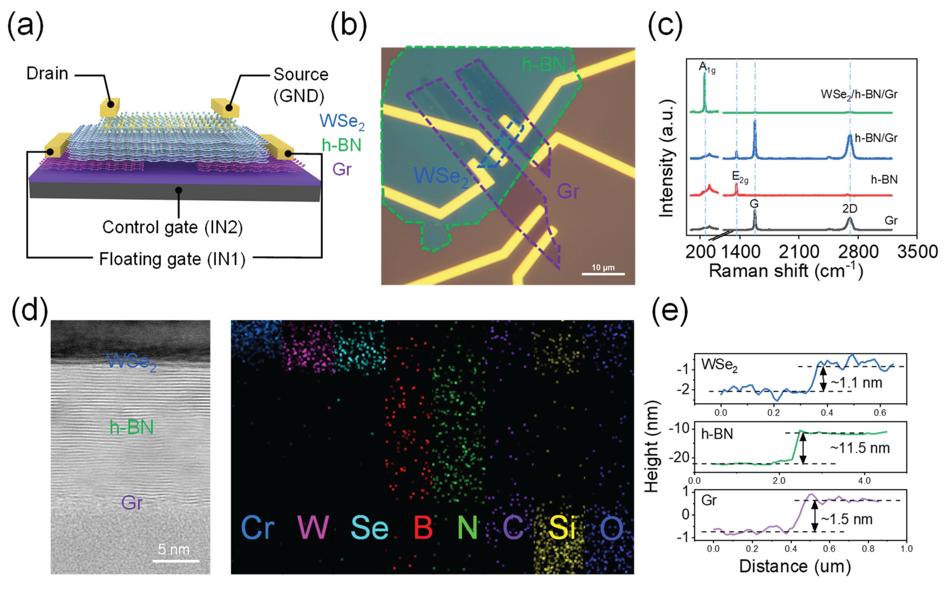
Figure 2.
Transport properties of the device. (a) Output curves under various floating-gate voltage; (b) Transfer curves under the modulation of floating gate at 0.3 V bias; (c) Transfer curves under the modulation of back gate at 0.3 V bias; (d), (g) IV curves with floating gate at 8/-8 V and back gates at 30 V and -60 V; (e), (h) IV Curves with back gate at 30/-60 V and floating gates at 8 V and -8 V; (f) Transfer curves under the modulation of floating gate at 0.3 V bias and back gates at 30 V and -60 V; (i) Transfer curves under the modulation of floating gate at 3 V bias and back gates at 30 V and -60 V.
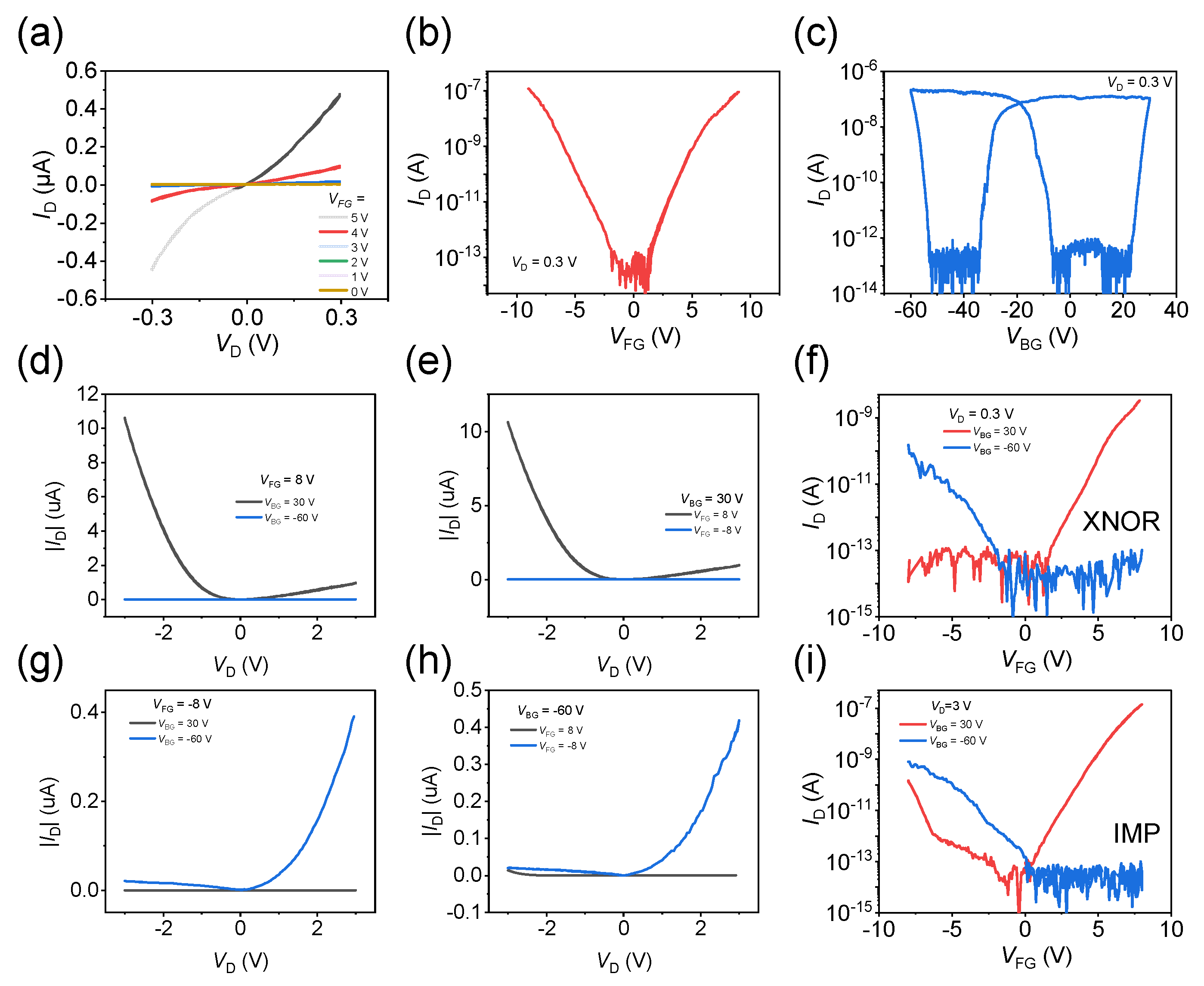
Figure 3.
Working principle of the reconfigurable logic device. (a), (b) Schematic illustration of charge carrier distribution at 0.3 V and 3 V bias, respectively. The red circles represent holes, and blue circles represent electrons. From top to bottom, the device is structured as WSe2, h-BN, Gr, SiO2, and Si. The solid arrow indicates the direction of electron injection; (c) Energy band diagram for electron tunnelling at -60 V and 30 V back-gate voltage; The floating-gate voltage is -8 V and the VD is 3 V; (d) Tunneling current as a function of VD with the floating-gate voltage set to -8 V and back-gate voltage set to -60 V/30 V.
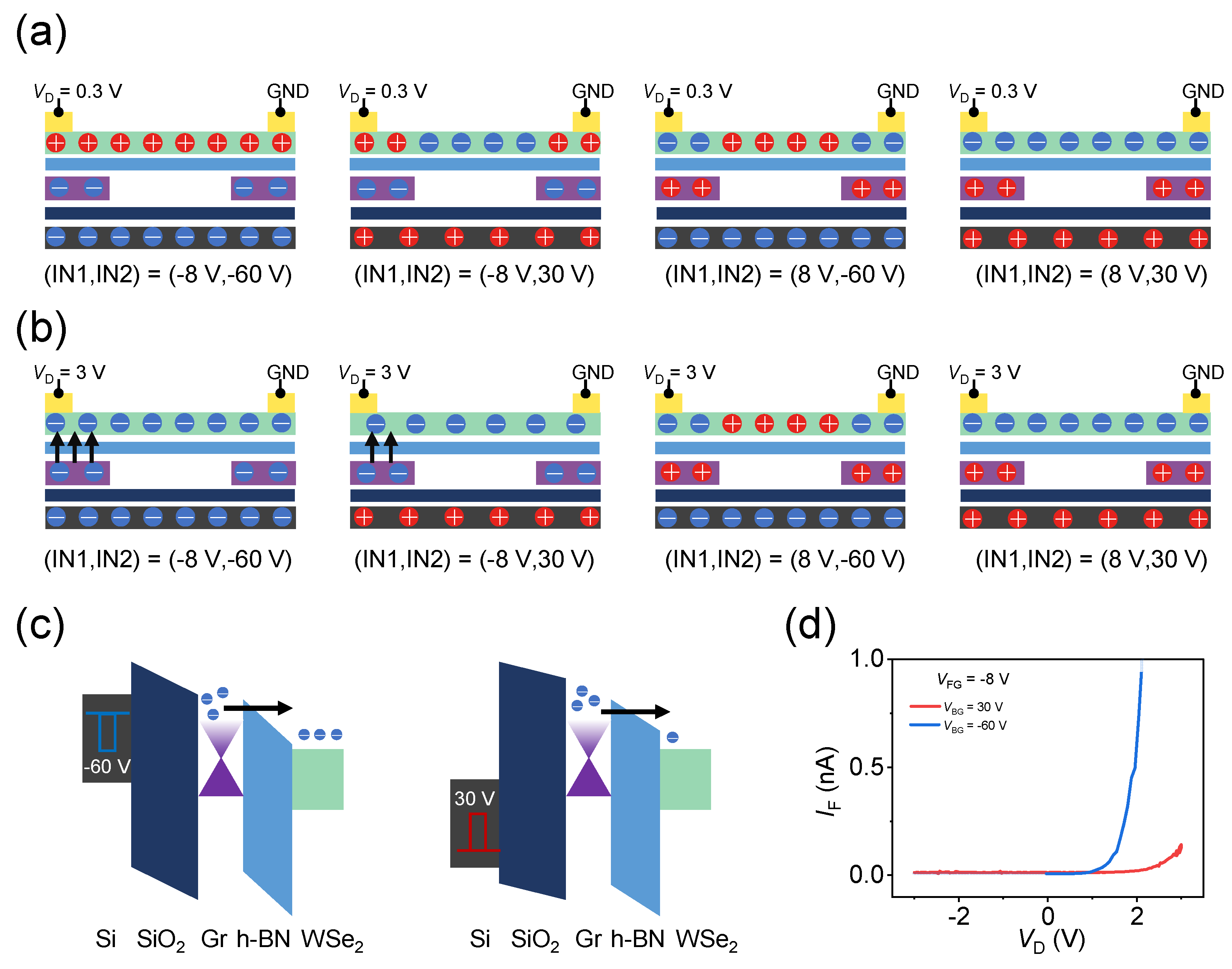
Figure 4.
Reconfigurable logic gate operation between XNOR and IMP. (a) Current-voltage (I-V) tunneling characteristics for WSe2/h-BN/Gr heterostructure; (b), (c) The ln(IF/V2FG) versus 1/VFG curves under negative and positive floating-gate voltages; (d) Transfer curves under the modulation of floating gate at various VD; (e) Truth table for the reconfigurable logic gates XNOR and IMP; (f) Transition between XNOR and IMP logic gates.
Disclaimer/Publisher’s Note: The statements, opinions and data contained in all publications are solely those of the individual author(s) and contributor(s) and not of MDPI and/or the editor(s). MDPI and/or the editor(s) disclaim responsibility for any injury to people or property resulting from any ideas, methods, instructions or products referred to in the content. |
© 2026 by the authors. Licensee MDPI, Basel, Switzerland. This article is an open access article distributed under the terms and conditions of the Creative Commons Attribution (CC BY) license (http://creativecommons.org/licenses/by/4.0/).
Copyright: This open access article is published under a Creative Commons CC BY 4.0 license, which permit the free download, distribution, and reuse, provided that the author and preprint are cited in any reuse.


