
Submitted:
20 January 2026
Posted:
21 January 2026
You are already at the latest version
Abstract
To address the challenges of ambient light interference and slow overload recovery in transimpedance amplifiers (TIAs) for automotive Light Detection and Ranging (LiDAR) systems, this paper proposes a high-performance TIA with integrated ambient light cancellation and fast recovery capabilities. The core design includes an adaptive ambient light cancellation (ALC) loop that eliminates background currents up to 3 mA without relying on AC coupling capacitors, achieving a low-frequency cutoff frequency of 321 kHz to ensure the signal-to-noise ratio (SNR) of weak target signals. A multi-stage clamping and current transfer mechanism is employed to realize rapid overload recovery: under 100 mA heavy overload conditions, the recovery time is controlled within 8.7 ns, and the pulse broadening is limited to 2.7 ns, avoiding measurement blind zones. Implemented in a 0.18-\( \mu \)m SiGe BiCMOS process, the proposed TIA occupies a compact area of 0.15 mm^2, with a transimpedance gain of 80 dB\( \Omega \) (10 kΩ) and a -3 dB bandwidth of 421 MHz. The input-referred noise current spectral density is 4.7 pA/√Hz, and the integrated equivalent input noise current from 1 Hz to 250 MHz is 73.6 nArms. Operating over a temperature range of -40 ℃ to 125 ℃, the TIA meets the rigorous requirements of automotive-grade applications. Performance comparisons with commercial products and state-of-the-art designs validate its superior ambient light rejection and fast recovery performance, making it suitable for direct time-of-flight (dToF) LiDAR systems in autonomous driving.
Keywords:
automotive LiDAR
; transimpedance amplifier (TIA)
; ambient light cancellation
; fast overload recovery
; SiGe BiCMOS process
1. Introduction
As autonomous driving technology advances to Level 4 (L4) and higher grades, the vehicle-mounted LiDAR, as a core sensor for environmental perception, has its detection accuracy, anti-interference capability and real-time response performance directly determine driving safety [1,2,3]. Direct Time of Flight technology has become the mainstream solution for vehicle-mounted LiDAR due to its longdetection range and high resolution. The Transimpedance Amplifier (TIA), as the core unit of the analog front end, undertakes the key task of converting the nanoampere-level weak photocurrent output by the Avalanche Photodiode (APD) into processable voltage signals. Its performance directly restricts the detection distance,dynamic range and signal fidelity of LiDAR [4,5,6].
Figure 1 shows the typical application scenario of the TIA chip in the LiDAR system. The weak current signal output by the photode tector after receiving reflected light completes current-to-voltage conversion and preliminary amplification via the TIA. The Fully Differential Amplifier (FDA) further suppresses common-modenoise and adjusts signal levels to match the input range of the Analog-to-Digital Converter (ADC). The ADC converts continuous analog signals into discrete digital signals, capturing time-domain characteristics of there flected waveform such as amplitude and edge shape completely. Finally, the Digital Signal Processor (DSP) or Field Programmable Gate Array (FPGA) calculates the time of flight through algorithms including time-domain correlation and frequency-domain transformation, and inversely derives target reflectivity and surface characteristics from waveform information simultaneously, realizing multi-target discrimination and anti-interference optimization.
The complexity of vehicle-mounted scenarios poses dual stringent challenges to TIAs: On the one hand, LiDAR needs to operate stably under extreme illumination conditions such as direct strong light and multi-light source superposition. Ambient light causes the APD to generate microampere to milliampere-level background current, which, when superimposed with weak signals reflected by targets, easily occupies the TIA’s dynamic range, causes output baseline drift, and even drowns weak signals in noise, seriously affecting the detection of long-distance, low-reflectivity targets [7,8,9]. On the other hand, short-distance, high-reflectivity targets (e.g., preceding vehicles, road signs) produce strong reflected light, making the TIA input current far exceed the linear operating range and enter an overload state. A slow recovery speed will lead to "blind zones" in subsequent signal processing and damage the real-time measurement continuity of high-sampling-rate LiDAR, which is unacceptable for vehicle-mounted scenarios requiring rapid response to sudden obstacles [10,11,12].
Existing studies have explored solutions to the above problems: Some TIAs adopt AC coupling to isolate the DC component of ambient light, but the additional coupling capacitor not only occupies extra board space but also degrades the overload recovery speed [13,14]. The ambient light suppression scheme based on a DC servo loop can achieve dynamic cancellation but has risks of compensation delay and signal distortion [15,16]. In terms of overload recovery, traditional clamp protection circuits mostly rely on a simple current bleeding mechanism, which is difficult to balance recovery speed and signal integrity, often resulting in excessive pulse broadening after overload and introducing additional ranging errors [17,18]. Although existing schemes have made progress in indicators such as gain and bandwidth, TIA designs that can simultaneously achieve efficient ambient light elimination and nanosecond-level fast recovery remain scarce, failing to fully meet the rigorous scenario requirements of vehicle-mounted LiDAR [19,20].
To address the above bottlenecks, this paper proposes a high-performance transimpedance amplifier for vehicle-mounted LiDAR systems, with core innovations focusing on two key characteristics: ambient light elimination and fast recovery. By integrating an adaptive ambient light cancellation loop, it can accurately offset background currents within 3 mA without AC coupling capacitors, with a low-frequency cutoff frequency of 321 kHz, ensuring the signal-to-noise ratio for weak signal detection. A multi-stage clamping and current transfer mechanism is designed, controlling the TIA’s recovery time within 8.7 ns under 100 mA heavy overload conditions, with pulse broadening not exceeding 2.7 ns. The proposed TIA is implemented based on a 0.18-m BiCMOS process, with a circuit area of only 0.15 mm2, a transimpedance gain of 80 dB, and a -3 dB bandwidth of 421 MHz, fully meeting the requirements of automotive-grade applications.
2. Core Structure of the Transimpedance Amplifier
Figure 2 illustrates the main architecture of the TIA proposed in this design. The key performance metrics of the circuit including working principle, gain, bandwidth, stability, and noise are elaborated as follows:
In Figure 2, the resistor , acts as the feedback resistor of the TIA. The internal amplifier of the TIA consists of a common emitter gain stage formed by bipolar junction transistor (BJT) and an emitter follower stage formed by . The common emitter stage provides the overall gain of the amplifier, and the load of the amplifying adopts a current source load composed of and emitter degeneration resistor . The emitter follower stage isolates the load effect caused by and the input capacitance of the subsequent stage. The output of the TIA in this design needs to drive the ALC loop and the subsequent fully differential amplifier (FDA) circuit. To mitigate stability issues and enhance load driving capability, a third stage emitter follower is introduced as the output stage of the TIA.
2.1. Gain
Under the effect of the feedback component , the operational amplifier operates in deep negative feedback. The voltage at node X is almost virtually shorted to AC ground in the AC domain, meaning that the variation of the input signal generates an output voltage variation at node Z. The transimpedance gain of the feedback TIA is approximately equal to the value of the feedback resistor .
2.2. Bandwidth
In the above design, utilizes a large device size and achieves high voltage gain from node X to node Y. The node impedance at node Y is the parallel combination of the output impedance of , the output impedance of with source degeneration resistor, and the input impedance of the follower . Thus, the gain from node X to node Y is nearly equal to the intrinsic gain of , which is also the gain of the internal operational amplifier of the TIA:
Benefiting from the sufficiently high intrinsic gain of the BJT, the Miller multiplied capacitance of the parasitic capacitance at nodes X and Y (mainly composed of the collector junction capacitance , of and the junction capacitance of the Schottky diode described in the next section) becomes the dominant pole capacitance. The bandwidth of the TIA is given by:
Due to the extremely high intrinsic gain of the BJT, a relatively large equivalent capacitance exists at the input terminal. To achieve better overload response (described in the next subsection), this design does not suppress the Miller effect, which has a significant impact on bandwidth performance. On the other hand, the bandwidth of this design is relatively independent of the parasitic capacitance of most APD products, endowing the circuit with additional characteristics.
2.3. Stability
Referring to the classical second order system model in control theory, to ensure ideal response speed and stability of the feedback system, the secondary pole formed at circuit node Y is required to be sufficiently far from the dominant pole of the loop. The secondary pole could be expressed as:
The impedance at node Y is almost equal to the output impedance of , and represents the parasitic capacitance of the node. Since the output impedance of the BJT is inversely proportional to the bias current, ideal stability at the rated bandwidth requires a sufficiently large bias current.
2.4. Noise
The equivalent input noise current of the TIA can be derived by first converting the open-circuit output noise voltage of the operational amplifier into the amplifier’s equivalent input noise voltage and equivalent input noise current via the amplifier’s voltage gain and transimpedance gain, respectively. Finally, the total equivalent input noise current of the TIA is obtained by scaling through the TIA’s transimpedance gain, i.e., .
Noise is a metric that follows the barrel effect; components contributing a small proportion to the total noise should not be the focus of practical design. It is observed that the output noise of the emitter follower formed by and is referred to the input through the gain of the common-emitter stage, resulting in negligible noise contribution from these two transistors.
Given the signal characteristics of the TIA, the input signal current operates in current sink mode: the current signal generated by optical illumination on the APD is either present or absent, with no negative current component. Thus, the downward swing at node Y is nearly useless. For this reason, the design employs the largest feasible degeneration resistor to mitigate the impact of on noise performance. As a result, only and the feedback resistor serve as the primary noise sources.
Figure 3 presents the noise model of the BJT, where denotes the shot noise of the emitter junction, represents the thermal noise of the base series resistance, and indicates the shot noise of the collector junction. By referring to the input port using the transconductance and current gain of , we obtain the total equivalent input noise voltage and equivalent input noise current of the operational amplifier (i.e., ):
The total input noise current of the TIA is given by:
This reveals a trade-off between noise and stability. Ideal noise performance requires minimizing the shot noise of the emitter junction, which demands a sufficiently small bias current of .
3. Fast Recovery Circuit Design
The proposed recovery circuit is implemented by embedding protection devices including Schottky diode , and , and protection resistor into the core TIA circuit. The TIA circuit with the added protection scheme is illustrated in Figure 4.
The working principle of the proposed protection circuit is as follows: When the input current slightly exceeds the linear input range of the circuit under the condition of mild overload, the overload signal makes the potential of node Z rise to a value where is higher than the emitter junction forward voltage of transistor . Then is turned on, which clamps the potential of node Z near . In this case, the circuit will not output an excessive voltage signal to cause the overload of the subsequent circuit.
A further rise in the potential of node Y causes the emitter follower to turn off. Eventually, the deep negative feedback of the amplifier induced by the feedback resistor disappears, and the characteristics of virtual short and virtual open at node X are lost. The circuit is converted into an open-loop common-emitter amplifier consisting of . During this process, most of the overload current is provided by the emitter junction of . When the overload signal disappears, the quiescent operating points of node Y and node Z are recovered by and that do not enter the saturation region.
When the input current reaches the range of several milliamperes, the potential of node Y rises and the potential of node X decreases, which makes the Schottky diode start to conduct. At this time, the overload current is provided by the collector junction of .
When the input current falls into the range of 10 mA to 100 mA, the voltage drop formed by the overload current across the protection resistor causes the emitter potential of to decrease. enters the active region and starts to divert more input current to the positive power supply. When the overload signal disappears, the quiescent operating points of node Y and node Z are also recovered by and that do not enter the saturation region.
Key considerations for the above design: (1) The resistance value of protection resistor and the junction capacitance of Schottky diode will degrade the circuit bandwidth to a certain extent. also contributes additional noise to the circuit. However, an excessively small requires with sufficient current capability to provide the required current for turning on , which may exceed the maximum sustainable current of . (2) The device area of should be sufficiently large to provide a current output capability of 100 mA. Accordingly, must be able to supply a maximum current of 1 mA to ensure the normal operation of , with a certain response speed to guarantee the fast recovery performance of the circuit. (3) The quiescent operating point of node Z is almost affected by the Process, Voltage and Temperature (PVT) variations of all devices. The expression of is given by Equation (8). It can be observed that the emitter junction voltage drop of , the current gain of , and the resistance value of all vary with temperature. The process corner deviation of alters the value of , thereby affecting the magnitude of the base current . The resistance value of itself has a tolerance of under different process corners, and the supply voltage directly impacts the value of .
The output swing of the TIA is determined by the magnitude of . To prevent the clamping effect of transistor from making the TIA output swing too small under certain PVT conditions and losing the clamping function under other PVT conditions which would cause overload of the subsequent circuit, the bias voltage requires a unique design to track PVT variations. Figure 5 illustrates the generation scheme of bias voltages and .
In the figure above, is generated by the voltage drop of current across resistor and diode . Capacitor is set to 30 pF to ensure the stability of node under transient overload of 100 mA. The expression of is given by Equation (9).
From the above equation, it can be concluded that by using the same devices as those in the amplifier circuit and adjusting the magnitudes of the positive and negative temperature coefficient currents as well as the resistance values of and , approximately consistent swing characteristics can be obtained under different PVT conditions.
4. Ambient Light Cancellation Circuit Design
Figure 6 illustrates the implementation principle of the ambient light cancellation function. The circuit employs an error amplifier to compare the output of the transimpedance amplifier (TIA) with the reference voltage , and the resulting output voltage drives the PMOS transistor to generate a reverse compensation current for offsetting the quiescent current . Specifically, the ambient light cancellation loop incorporates an integrator low-pass filter to achieve low-pass characteristics, which enables the separation of the slowly varying quiescent current from the fast echo signal current . The reference voltage is derived from a dummy-TIA, which replicates the topology of another TIA circuit but operates without input signals. Excellent process voltage temperature (PVT) characteristics of can be achieved through layout matching.
Figure 7 presents the detailed implementation of the error amplifier. A simple folded cascode architecture is adopted. To match the input voltage range of transistor , a single-stage emitter follower composed of is introduced to shift the quiescent operating point upward by an emitter-base voltage drop .
The gain of the amplifier in Figure 7 is given by:
According to Equation (10), we can calculate the low-frequency cutoff of the loop using feedback theory. Assuming the transfer function of the transimpedance amplifier is given by the following equation, where denotes the dominant pole (i.e., the -3 dB bandwidth) of the TIA stage:
The transfer function of the feedback network formed by the error amplifier is given in (13), where is the pole formed by , , and the Miller effect, with :
Solving for the dominant pole from the denominator of the above equation gives the low-frequency cutoff of the ALC loop:
From Equation (14), it can be seen that to achieve a sufficiently low low-frequency cutoff for the ALC loop, a larger time constant formed by and is required.
5. Post-Layout Simulation Results
This design is implemented based on a 180 nm SiGe process. Figure 8 presents the layout of the proposed design. Figure 9 and Figure 10 illustrate the transient simulation waveform and AC simulation waveform of the core TIA circuit respectively, under the conditions of 3.3-V supply voltage, typical typical (TT) process corner and room temperature. A pulse excitation with an amplitude of 50 A is applied in the transient simulation to mimic the actual signal. The results demonstrate that the proposed design achieves a transimpedance gain of nearly 10 k and a bandwidth of 421 MHz.
Figure 11 presents the noise performance simulation results of the proposed design. The simulation results show that the equivalent input noise current integrated from 1 Hz to 250 MHz is 73.6 . The equivalent input noise current spectral density scaled by the 10 transimpedance gain and bandwidth is 4.65 .
Figure 12 illustrates the output of the transimpedance amplifier under the overload current with an amplitude of 100 mA and a half pulse width of 6 ns under different PVT conditions. The three PVT configurations are as follows: (i) Supply voltage is 3.15-V, temperature is , and the process corners of resistors, capacitors, NPN transistors and PNP transistors are set as slow. (ii) Supply voltage is 3.3-V, temperature is , and the process corners of resistors, capacitors, NPN transistors and PNP transistors are set as typical. (iii) Supply voltage is 3.45-V, temperature is , and the process corners of resistors, capacitors, NPN transistors and PNP transistors are set as fast. Under the typical process corner condition, the pulse broadening induced by severe overload is controlled to 2.6 ns, and the recovery time for the output to recover to 1% of the quiescent value after the overload disappears is 8.7 ns.
Figure 13 shows the AC simulation waveform of the TIA output with the ALC loop under a DC bias current () of 100 A. The simulation results demonstrate that the low-frequency cut-off frequency of the ALC loop is approximately 321 kHz. Meanwhile, the maximum quiescent current that can be eliminated by the ALC loop is mainly determined by the device size of transistor in Figure 6, which can be flexibly configured according to practical application scenarios.
Table 1 summarizes the performance metrics of this study and compares them with previous research. The table demonstrates the exceptional fast recovery performance and superior ambient light rejection capability of this work. The fast recovery time under heavy load conditions outperforms that of two mainstream commercial products [17,18]. It also achieves reasonable performance in other aspects, meeting the stringent requirements of automotive LiDAR scenarios.
6. Conclusions
This paper proposes a high-performance TIA for automotive dToF LiDAR, addressing ambient light interference and slow overload recovery. Integrating an adaptive ALC loop, it eliminates up to 3 mA background current (321 kHz low-frequency cutoff) without AC coupling capacitors. A multi-stage clamping-current transfer mechanism enables 8.7 ms recovery time and 2.7 ns pulse broadening under 100 mA overload. Implemented in 0.18- SiGe BiCMOS, the TIA features area, 80 dB gain, bandwidth, and input-referred noise, meeting automotive-grade ( to ) requirements. It offers a reliable analog front-end solution for autonomous driving LiDAR systems.
Author Contributions
Conceptualization, Y.L. and Q.L.; methodology, Y.L., and J.L.; software, Y.L.; formal analysis, Y.L. and Q.L.; data curation, Y.L. and Q.L.; writing—original draft preparation, Y.L.; writing—review and editing, Y.L., Q.L., and J.L. All authors have read and agreed to the published version of the manuscript.
Data Availability Statement
Data are contained within the article.
Conflicts of Interest
Author Jinghu Li was employed by the company Xiamen Eochip Seiconductor Co., Ltd. The remaining authors declare that the research was conducted in the absence of any commercial or financial relationships that could be construed as a potential conflict of interest.
References
- Ngo, T.H.; Kim, C.H.; Kwon, Y.J.; Ko, J.S.; Kim, D.B.; Park, H.H. Wideband Receiver for a Three-Dimensional Ranging LADAR System. IEEE Transactions on Circuits and Systems I: Regular Papers, 2013, 60, 448-456. DOI:10.1109/TCSI.2012.2215800. [CrossRef]
- Zheng, H.; Ma, R.; Liu, M.L.; Zhu. Z.M. High Sensitivity and Wide Dynamic Range Analog Front-End Circuits for Pulsed TOF 4-D Imaging LADAR Receiver. IEEE Sensors Journal, 2018, 18, 3114-3124. DOI:10.1109/JSEN.2018.2809795. [CrossRef]
- Aram, B.; Tarmo, R.; Juha, K. A Low Noise, Wide Dynamic Range TOF Laser Radar Receiver Based on Pulse Shaping Techniques. IEEE International Symposium on Circuits and Systems (ISCAS), 2018, 1-5. DOI: 10.1109/ISCAS.2018.8351606. [CrossRef]
- Wang, X.; Ma, R.; Li, D.; et al. A Low Walk Error Analog Front-End Circuit With Intensity Compensation for Direct ToF LiDAR. IEEE Transactions on Circuits and Systems I: Regular Papers, 2020, 67, 4309-4321. DOI:10.1109/TCSI.2020.3022714. [CrossRef]
- Hong, C.; Kim, S.H.; Kim, J.H. et al. A Linear-Mode LiDAR Sensor Using a Multi-Channel CMOS Transimpedance Amplifier Array. IEEE Sensors Journal, 2018, 18, 7032-7040. DOI:10.1109/JSEN.2018.2852794. [CrossRef]
- Tan, X.; Li, K.; Guo, J. A Low-Noise and High-Accuracy Transimpedance Amplifier Exploiting Power-on-Calibration Technique for LiDAR. IEEE Transactions on Instrumentation and Measurement, 2022, 71, 1-10. DOI:10.1109/TIM.2022.3186697. [CrossRef]
- Khoeini, F.; Hadidian, B.; Zhang, K.; et al. A Transimpedance-to-Noise Optimized Analog Front-End With High PSRR for Pulsed ToF Lidar Receivers. IEEE Transactions on Circuits and Systems I: Regular Papers, 2021, 68, 3642-3655. DOI:10.1109/TCSI.2021.3089098. [CrossRef]
- Wang, X.; Ma, R.; Li, D.; et al. A Wide Dynamic Range Analog Front-End With Reconfigurable Transimpedance Amplifier for Direct ToF LiDAR. IEEE Transactions on Circuits and Systems II: Express Briefs, 2023, 70, 944-948. DOI:10.1109/TCSII.2022.3220888. [CrossRef]
- Ma, R.; Liu, M.; Zheng, H.; et al. A 66-dB Linear Dynamic Range, 100-dBΩ Transimpedance Gain TIA With High-Speed PDSH for LiDAR. IEEE Transactions on Instrumentation and Measurement, 2020, 69, 1020-1028. DOI:10.1109/TIM.2019.2907776. [CrossRef]
- Guo, J.; Gao, Z.; Zeng, X.; et al. High Signal-to-Noise Ratio and High-Sensitivity 4-D LiDAR Imaging Receiver. IEEE Transactions on Very Large Scale Integration (VLSI) Systems, 2025, 33, 1437-1441.DOI:10.1109/TVLSI.2024.3498867. [CrossRef]
- Zheng, H.; Ma, R.;Wang, X.; et al. A Linear-Array Receiver AFE Circuit Embedded 8-to-1 Multiplexer for Direct ToF Imaging LiDAR Applications. IEEE Transactions on Circuits and Systems I: Regular Papers, 2022, 69, 5050-5058. DOI:10.1109/TCSI.2022.3204639. [CrossRef]
- Chang, Y.P.; Liu, C.N.; Pei, Z.; et al. New scheme of LiDAR-embedded smart laser headlight for autonomous vehicles. Optics Express, 2019, 27, A1481-A1489. DOI:10.1364/OE.27.0A1481. [CrossRef]
- Williams, G.M.; Jr.Optimization of eyesafe avalanche photodiode lidar for automobile safety and autonomous navigation systems. Optical Engineering, 2017, 56, DOI:10.1117/1.OE.56.3.031224. [CrossRef]
- Kameyama, S.; Hirai, A.; Imaki, M.; et al. Demonstration on range imaging of 256 x 256 pixels and 30 frames per second using short wavelength infrared pulsed time-of-flight laser sensor with linear array receiver. Optical Engineering, 2017, 56, DOI:10.1117/1.OE.56.3.031214. [CrossRef]
- Kurtti, S.; Baharmast, A.; Jansson, J.K.; et al. A Low-Noise and Wide Dynamic Range 15 MHz CMOS Receiver for Pulsed Time-of-Flight Laser Ranging. IEEE Sensors Journal, 2021, 21, 22944-22955. DOI:10.1109/JSEN.2021.3105447. [CrossRef]
- Cho, H.S.; Kim, C.H.; Lee, S.G. A High-Sensitivity and Low-Walk Error LADAR Receiver for Military Application. IEEE Transactions on Circuits and Systems I: Regular Papers, 2014, 61, 3007-3015. DOI:10.1109/TCSI.2014.2327282. [CrossRef]
- Analog Devices. LTC6560 Single Channel Transimpedance Amplifier with Output Multiplexing, Datasheet Rev. B, 2025. [Online]. Available: https://www.analog.com/en/products/ltc6560.html, Accessed: January 16, 2026.
- Texas Instruments. LMH32404 Four-Channel, Differential Output, Multiplexed Transimpedance Amplifier With Integrated Clamping and Ambient Light Cancellation, Datasheet Rev. C, Nov.16, 2022. [Online]. Available:https://www.ti.com/product/LMH32404/datasheet, Accessed: Jan. 16, 2026.
- Brigati, S.; Colombara, P.; D’Ascoli, L.; Gatti, U. A SiGe BiCMOS burst-mode 155-Mb/s receiver for PON. IEEE Journal of Solid-State Circuits, 2002, 37, 887-894, doi: 10.1109/JSSC.2002.1015687. [CrossRef]
- Ciftcioglu, B.; Zhang, J.; Zhang, L.; Marciante, J.R.; Zuegel, J.D.; Sobolewski, R.; Wu, H. 3-GHz silicon photodiodes integrated in a 0.18 μm CMOS technology. IEEE Photonics Technol. Lett, 2008, 20, 2069–2071, (https://doi/org/10.1109/LPT.2008.2006404). [CrossRef]
- Tadic, N. and Zimmermann, H. Optical Receiver With Widely Tunable Sensitivity in BiCMOS Technology. IEEE Transactions on Circuits and Systems I: Regular Papers, 2008, 55, 1223-1236, doi: 10.1109/TCSI.2008.916399. [CrossRef]
Figure 1.
ADC-Based System Scheme.
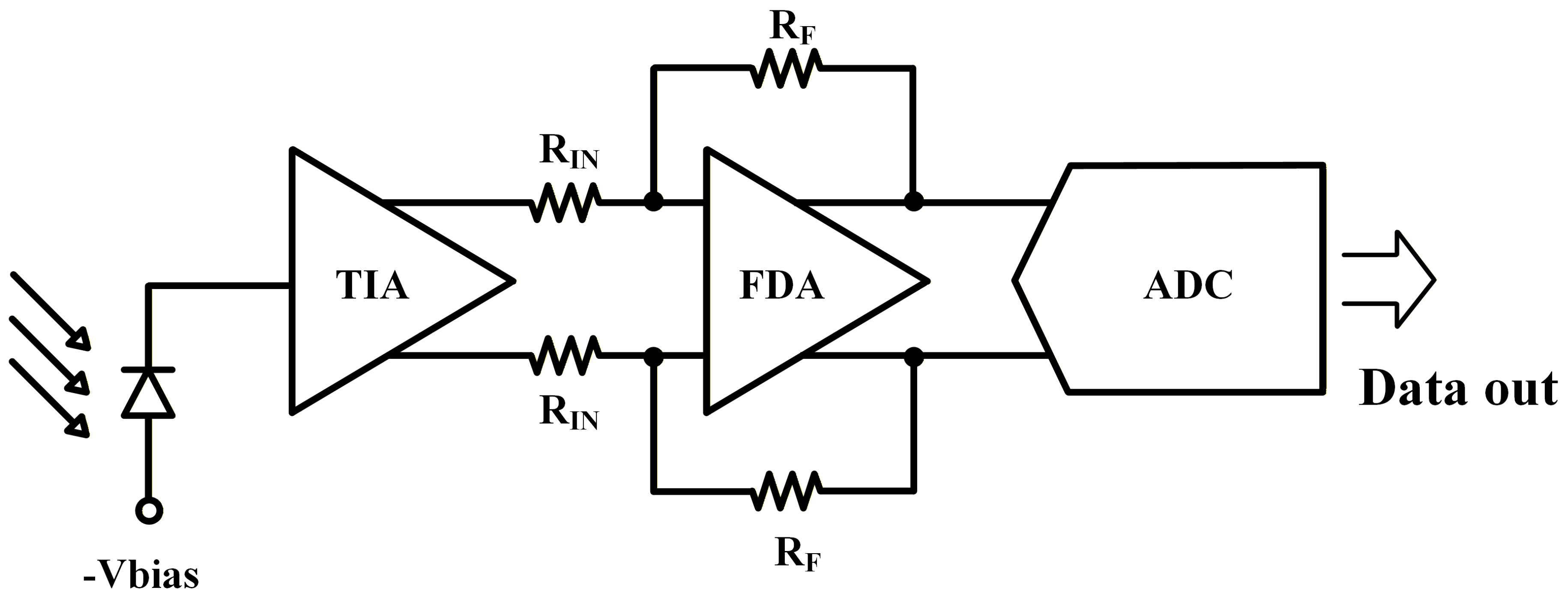
Figure 2.
Core Circuit Structure of the proposed TIA.
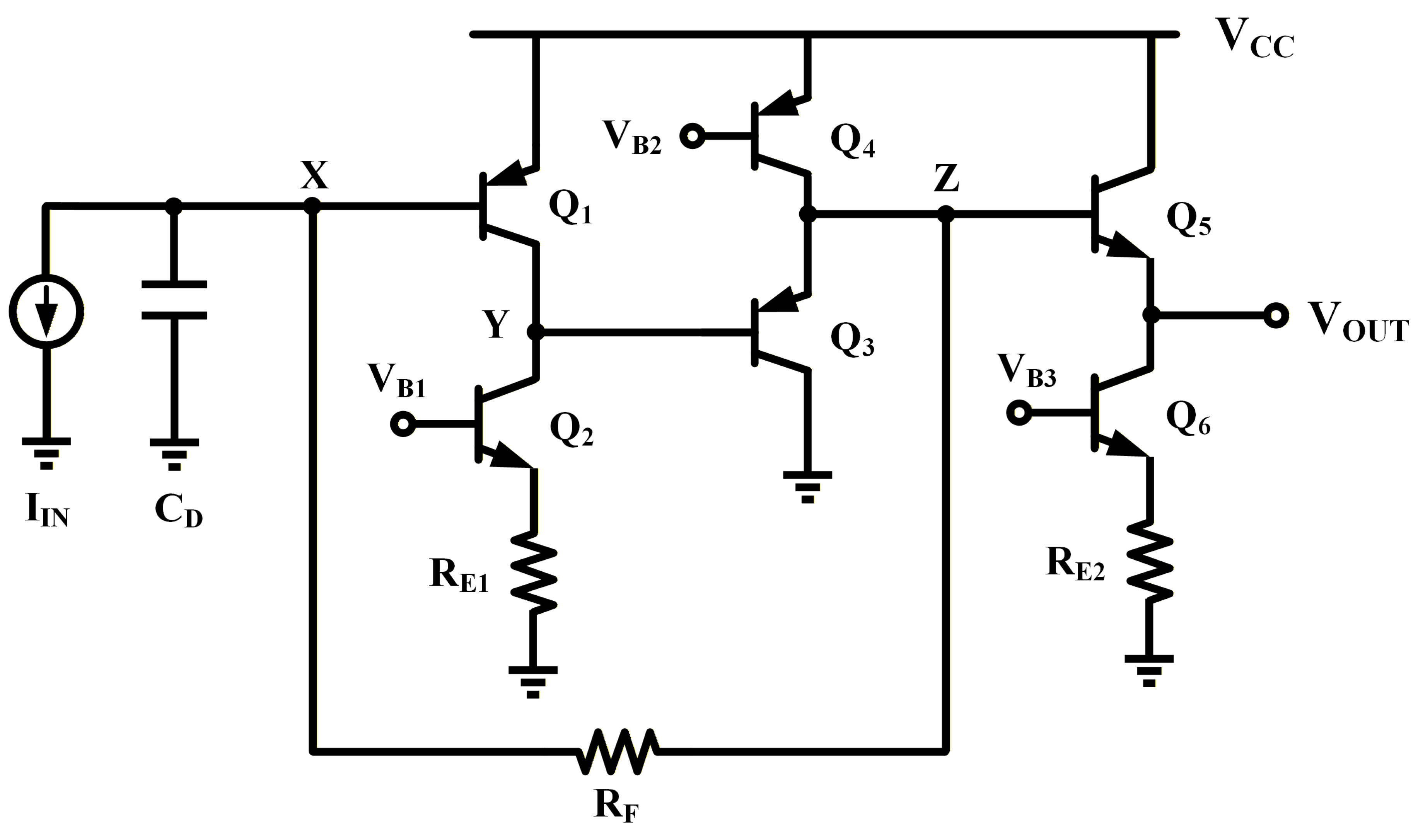
Figure 3.
The noise model of the BJT.
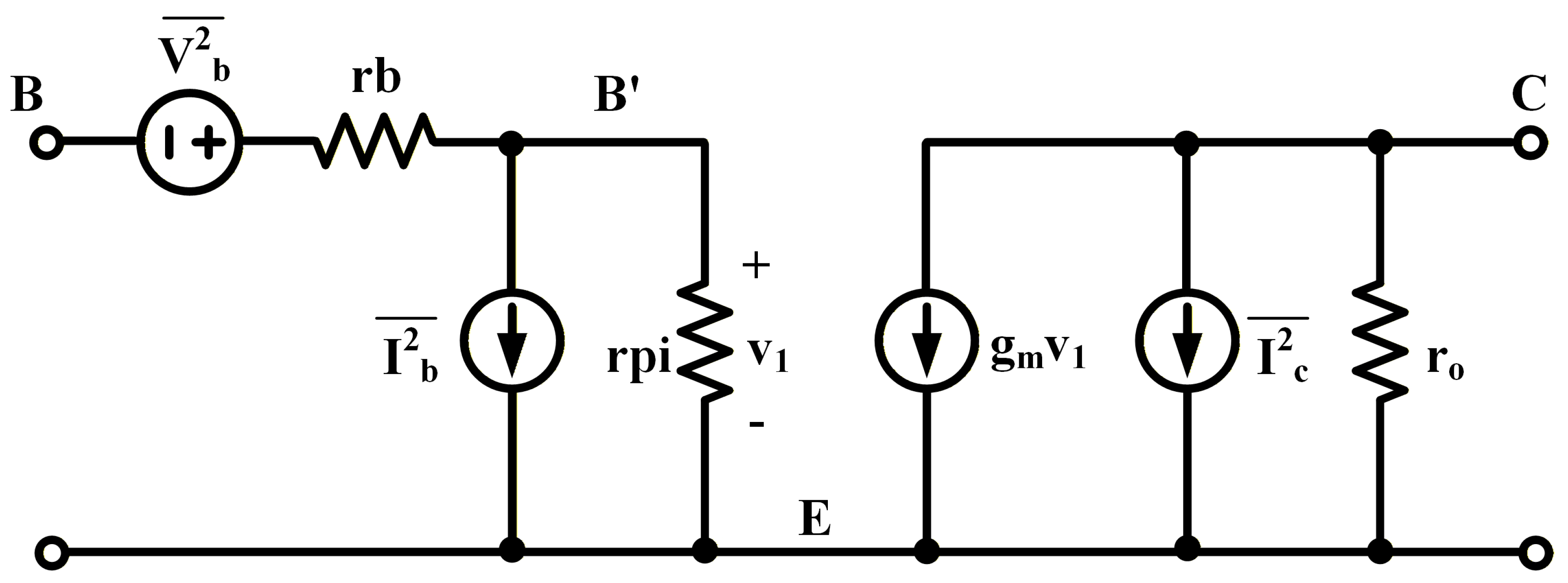
Figure 4.
Schematic Diagram of the TIA Core Circuit with Added Fast Recovery Circuit.
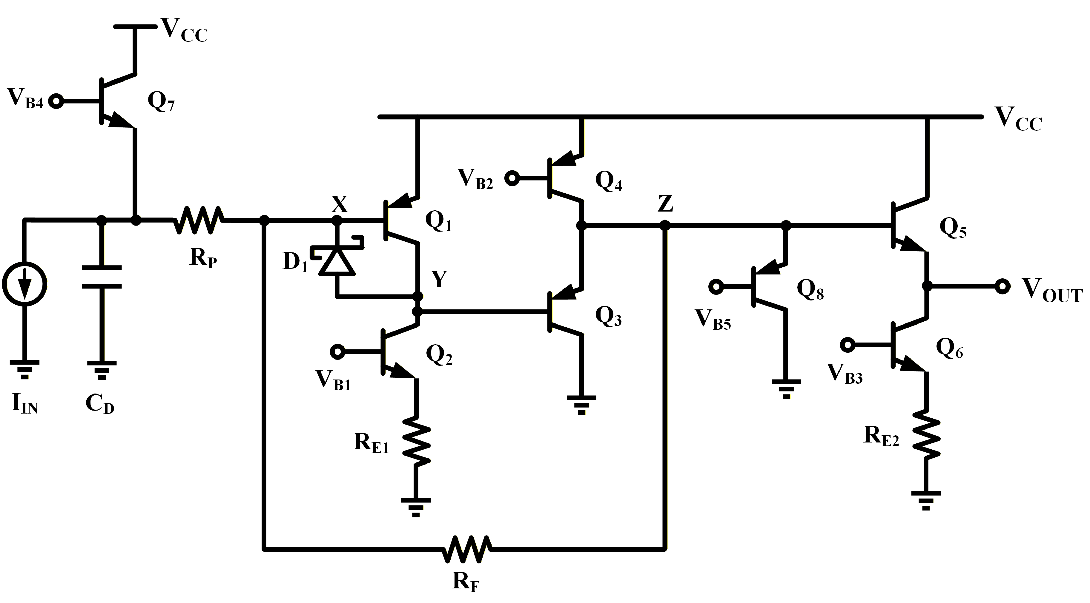
Figure 5.
Generation Method of Bias Voltages and .
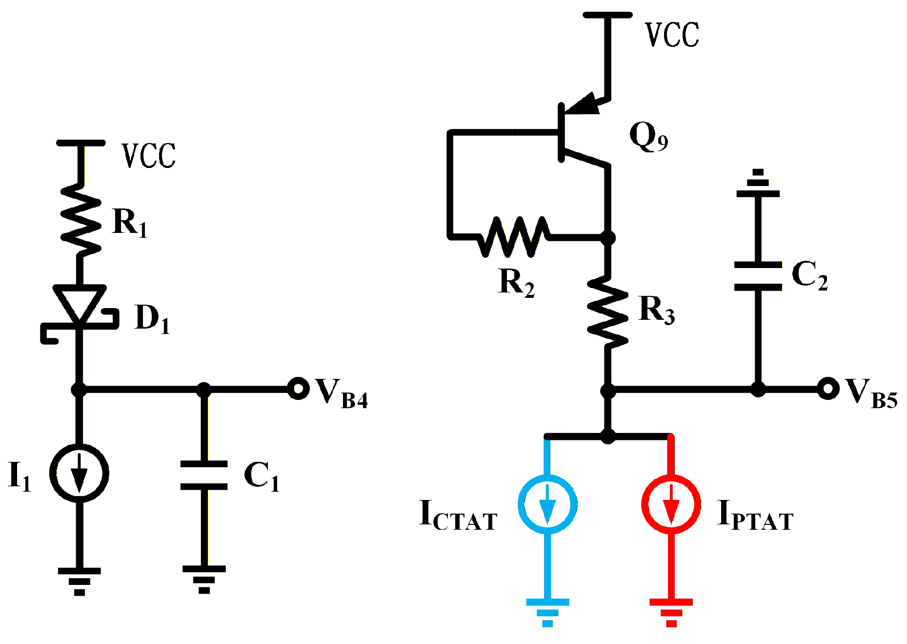
Figure 6.
Principle of ambient light cancellation circuit.
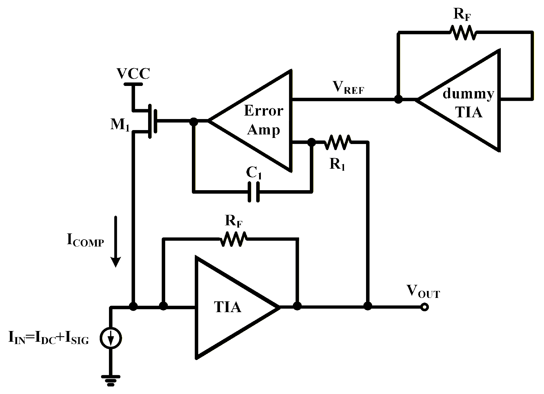
Figure 7.
Circuit structure of the error amplifier.
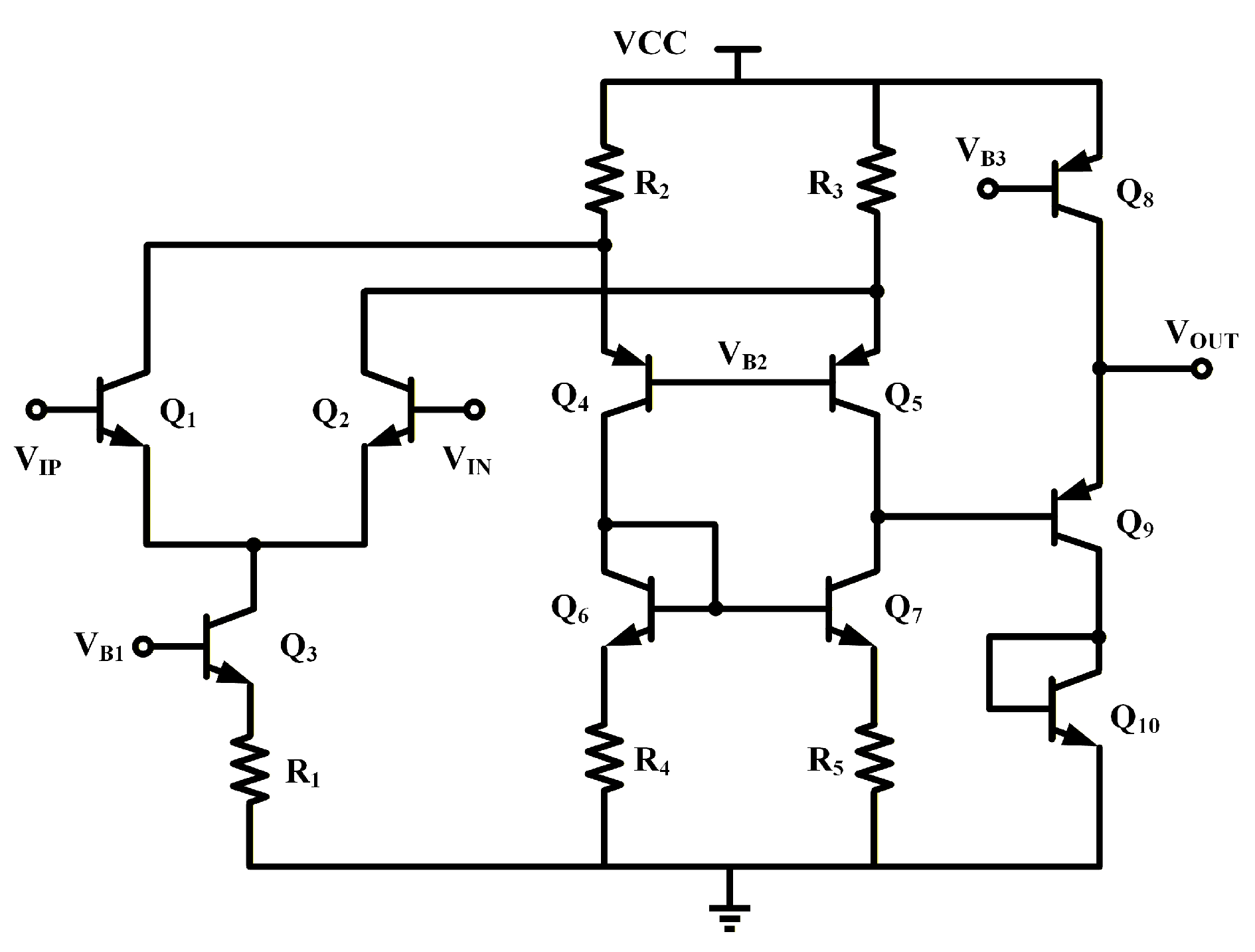
Figure 8.
Layout of the proposed TIA.
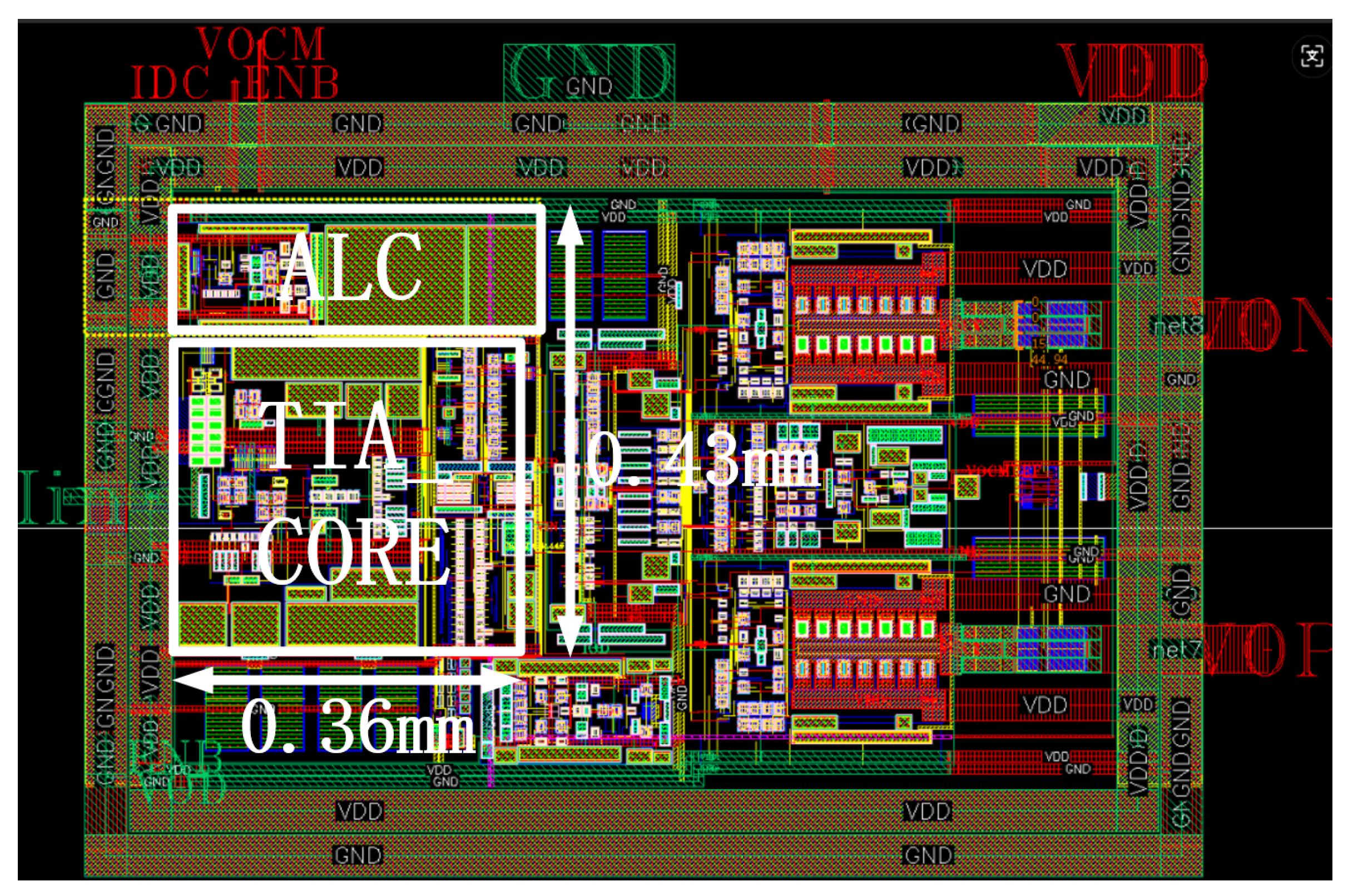
Figure 9.
Transient Simulation Results of the TIA Core Circuit.
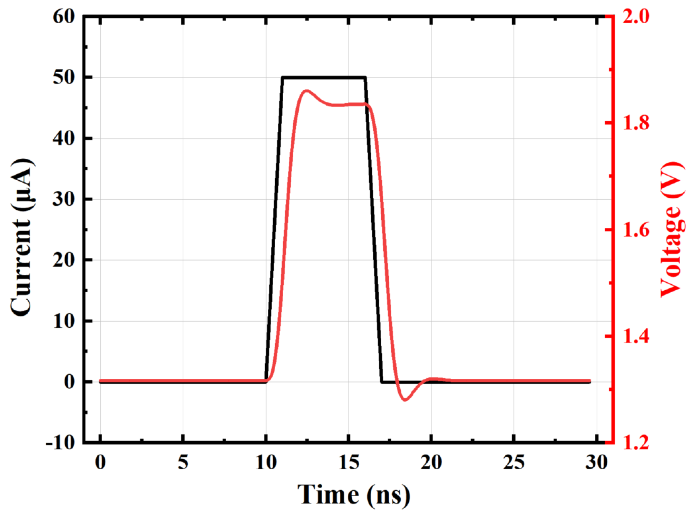
Figure 10.
AC Simulation Results of the TIA Core Circuit.
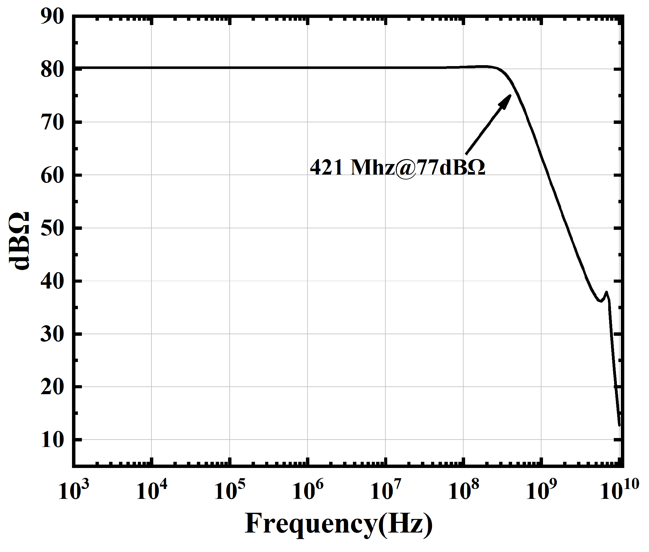
Figure 11.
Input-Referred Noise Current Power Spectral Density of the TIA.
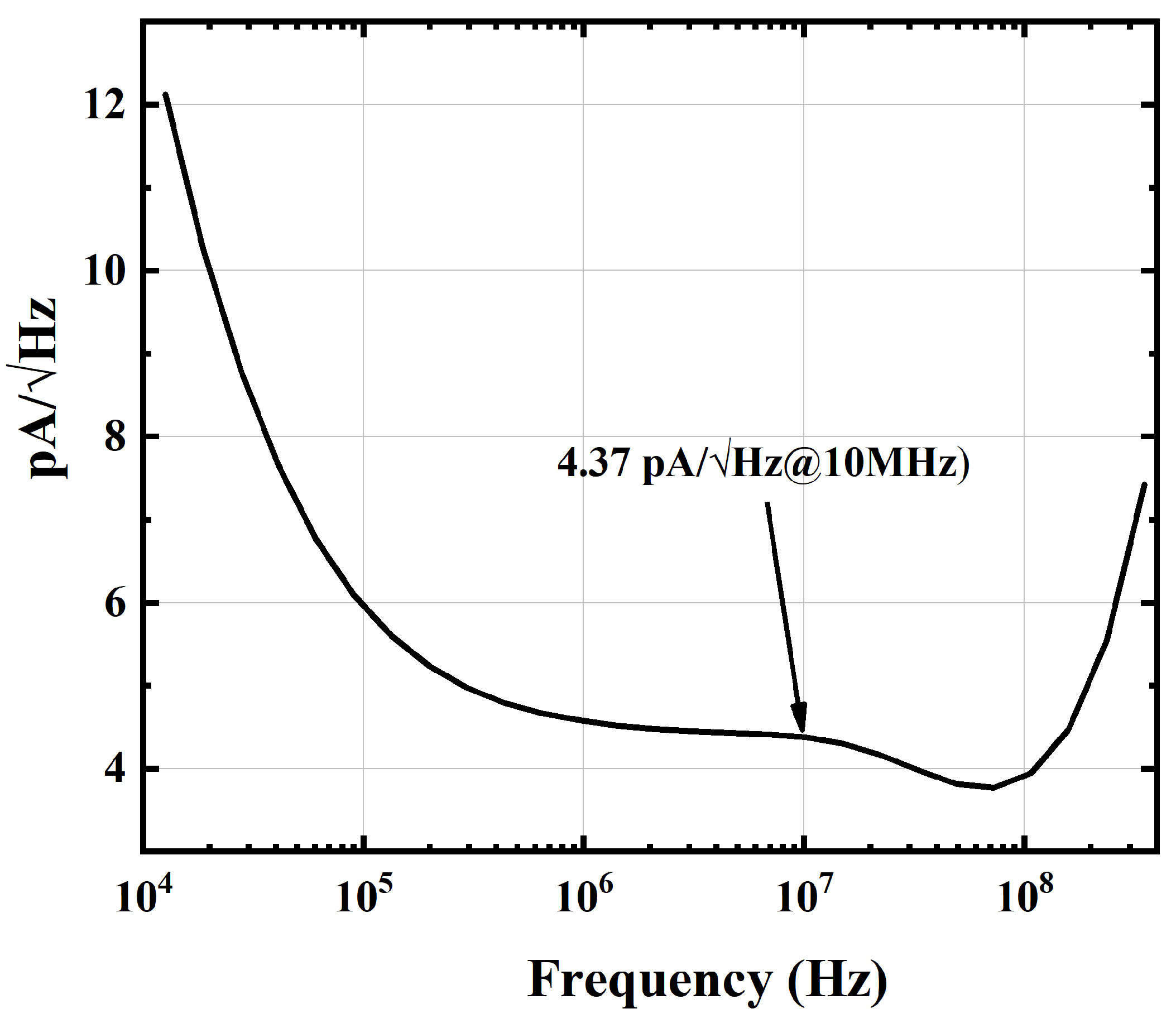
Figure 12.
Output of the Transimpedance Amplifier under a 100 mA Overload Current Across Different PVT Conditions.
Figure 12.
Output of the Transimpedance Amplifier under a 100 mA Overload Current Across Different PVT Conditions.
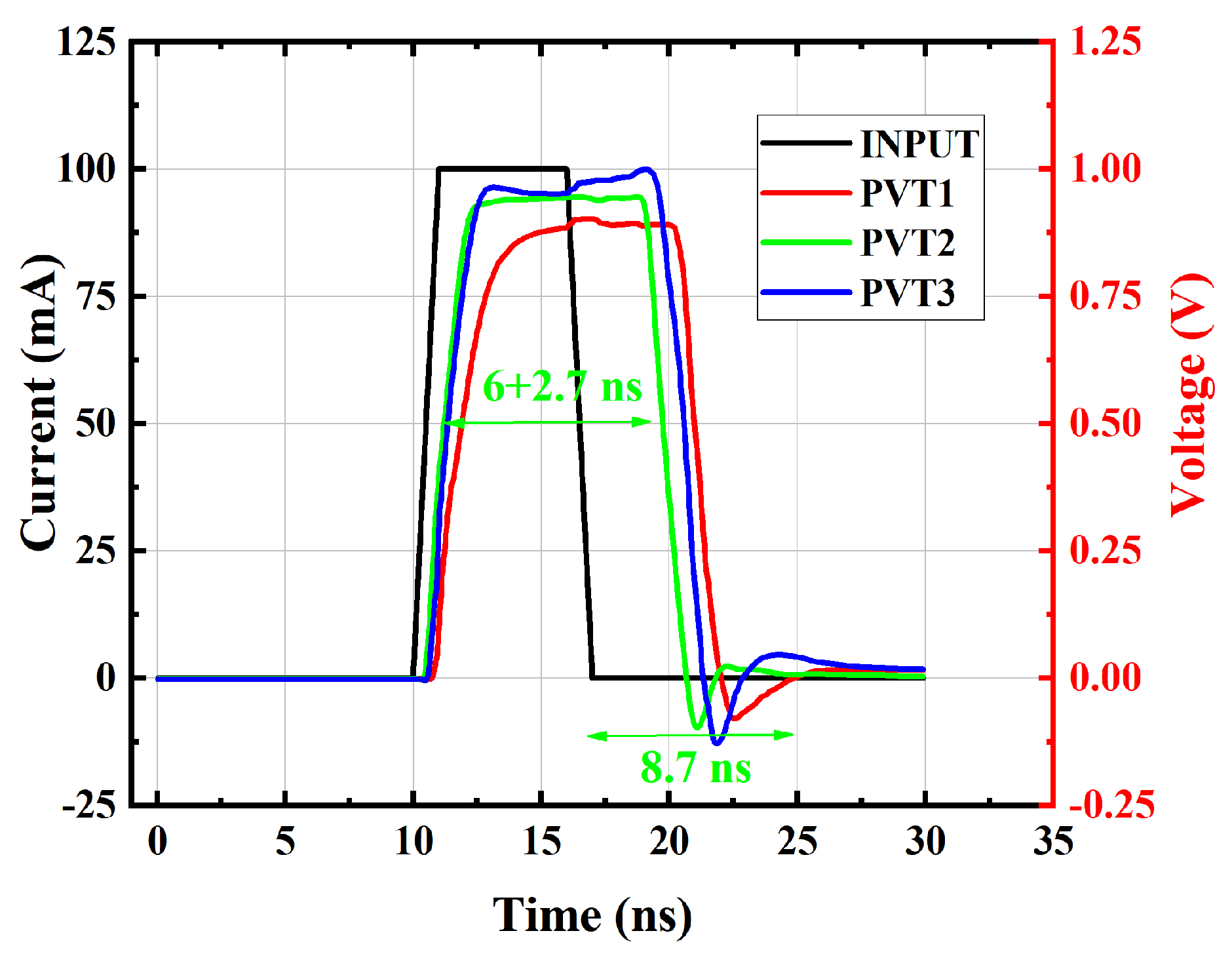
Figure 13.
Simulation Curve of the TIA Output with the ALC Loop in AC Analysis.
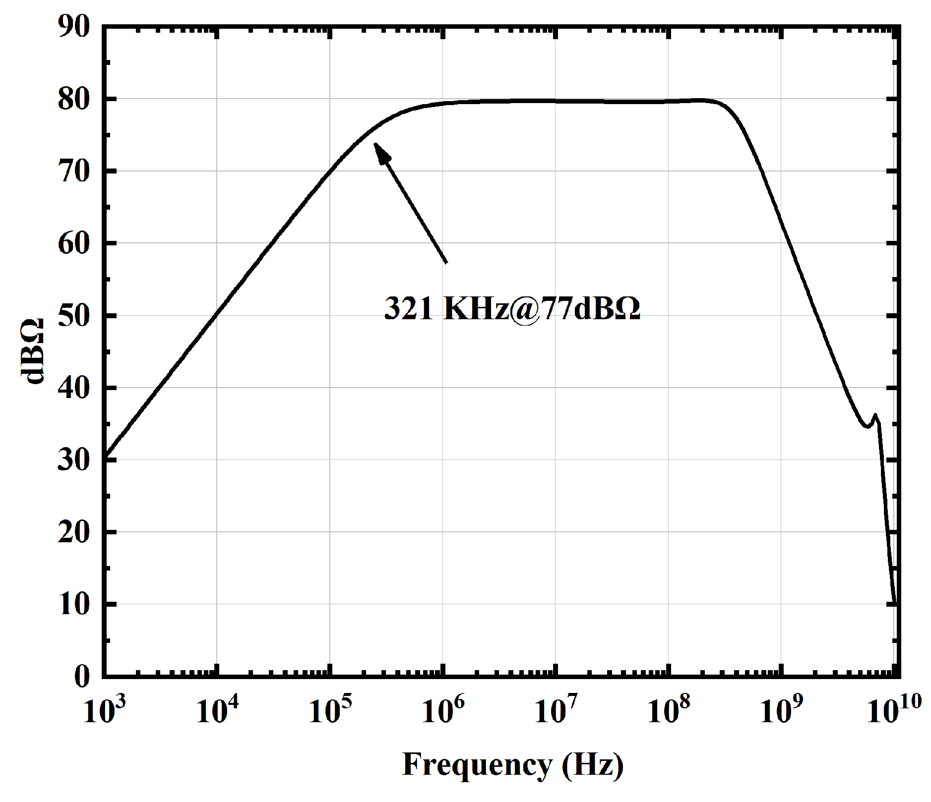

Table 1.
Performance comparison of this circuit with other circuits.
| Specification | LTC6560 [17] Commercial |
LMH32404 [18] Commercial |
Ref.[7] | Ref.[8] | Ref.[9] | This Work |
|---|---|---|---|---|---|---|
| Technology | − | − | ||||
| APD Capacitance (pF) | 2 | 1 | 1 | 1.5 | 2 | 1 |
| Active Area (mm2) | − | − | 0.023 | 0.012 | 0.35 | 0.15 |
| Power Dissipation (mW) | 90 | 92.4 | 41 | 29.4 | 8 | 46.2 |
| Bandwidth (MHz) | 220 | 350 | 300 | 260 | 110 | 421 |
| Transimpedance Gain () | 74 | 20 | 100 | 50 | 100 | 10 |
| Input-Referred Noise () | 4.8 | 3.54 | 3.67 | 3.3 | 2.21 | 4.7 |
| Ambient Light Rejection (kHz) | − | 400 | − | − | − | 321 |
| Max. Ambient Light Range (mA) | − | 2.5 | − | − | − | 3 |
| Fast Recovery Time (ns) | 10@10mA | 12@100mA | − | − | − | 8.7@100mA |
| Pulse Broadening (ns) | − | 5@100mA | − | − | − | 2.7@100mA |
Disclaimer/Publisher’s Note: The statements, opinions and data contained in all publications are solely those of the individual author(s) and contributor(s) and not of MDPI and/or the editor(s). MDPI and/or the editor(s) disclaim responsibility for any injury to people or property resulting from any ideas, methods, instructions or products referred to in the content. |
© 2026 by the authors. Licensee MDPI, Basel, Switzerland. This article is an open access article distributed under the terms and conditions of the Creative Commons Attribution (CC BY) license (http://creativecommons.org/licenses/by/4.0/).
Copyright: This open access article is published under a Creative Commons CC BY 4.0 license, which permit the free download, distribution, and reuse, provided that the author and preprint are cited in any reuse.


