
Submitted:
16 January 2026
Posted:
16 January 2026
You are already at the latest version
Abstract
This paper presents an all-digital fractional-N phase-locked loop (ADPLL) operating in the 2.86-3.2 GHz range, optimized for IoT and high-frequency RF transceiver applications demanding stringent phase noise performance, fast settling time, and high integration capability. The key innovation lies in the introduction of a bandpass delta-sigma time-to-digital converter (BPDSTDC) that achieves high-resolution phase detection, an extended detection range of ± 2π, and superior noise-shaping characteristics, completely eliminating the complex calibration procedures typically required in conventional TDC designs. The proposed architecture synergistically combines the BPDSTDC with digital down-conversion blocks to extract phase error at baseband, a divider chain integrated with phase interpolators achieving 1/4 fractional resolution to suppress in-band quantization noise, and a wide-bandwidth digital loop filter (>1 MHz) ensuring fast dynamic response and robust stability. The bandpass delta-sigma modulator is implemented with compact resonator structures and a flash quantizer, achieving an optimal balance among resolution, power consumption, and silicon area. The incorporation of highly linear phase interpolators extends fractional frequency synthesis capability without requiring complex digital-to-time converters (DTCs), significantly reducing design complexity and calibration overhead. Fabricated in a 180-nm CMOS technology, the proposed chip demonstrates robust measured performance. The band-pass delta-sigma TDC achieves a low integrated rms timing noise of 183 fs within a 1-MHz bandwidth. Leveraging this low TDC noise, the complete ADPLL exhibits a measured in-band phase noise of -120 dBc/Hz at a 1-MHz offset for a 3.2-GHz output frequency while operating with a loop bandwidth exceeding 1 MHz. This corresponds to a normalized phase noise of -216 dBc/Hz. The system operates from a 1.8-V supply and consumes 10 mW, achieving competitive performance compared with prior noise-shaping TDC-based all-digital PLLs.
Keywords:
all-digital fractional-N phase-locked loop (ADPLL)
; time-to-digital converter
; bandpass delta-sigma time-to-digital converter
; phase interpolators: quantization noise
; phase noise
1. Introduction
Phase-locked loops (PLLs) operating in the multi-gigahertz frequency range with low reference frequencies are essential building blocks in modern Internet-of-Things (IoT) and highly integrated RF transceiver systems [1,2]. Such applications impose increasingly stringent requirements on phase noise, settling time, power consumption, and scalability under advanced CMOS processes. In particular, the combination of low reference frequencies and wide output tuning ranges results in large division ratios, which significantly magnify the impact of phase detector and quantization noise on in-band phase noise performance. Therefore, the design of the phase detector block plays a crucial role in ensuring low phase jitter for the frequency synthesizer, especially when adhering to strict power and area constraints [3].
All-digital phase-locked loops (ADPLLs) have emerged as attractive alternatives to conventional analog PLLs due to their superior portability, programmability, and compatibility with digital CMOS scaling [4,5]. In ADPLLs, time-to-digital converters (TDCs) replace conventional phase-frequency detectors and charge pumps, enabling fully digital loop implementation. However, the finite resolution and limited detection range of conventional TDC architectures, typically based on delay lines or Vernier structures [6,7], introduce substantial quantization noise and nonlinearity within the PLL loop bandwidth. These effects become increasingly pronounced as the loop bandwidth is widened to achieve fast settling time, often necessitating complex background calibration schemes to mitigate PVT variations, mismatch, and nonlinearity [8]. Such calibration overheads increase design complexity, power consumption, and verification effort, undermining the scalability advantages of ADPLLs.
Delta-sigma noise-shaping techniques have been widely explored to relax the intrinsic resolution requirements of TDCs by redistributing quantization noise outside the PLL loop bandwidth [9,10]. Prior work has predominantly focused on low-pass delta-sigma TDC architectures, which shape quantization noise toward higher frequencies [11,12]. While effective in systems with sufficiently high reference frequencies and narrow loop bandwidths, low-pass noise shaping becomes less effective when the reference frequency is limited to tens of megahertz and the loop bandwidth must be expanded to meet fast locking requirements [13,14]. Under these conditions, the available out-of-band spectral region for noise shaping is constrained, leading to noise folding, elevated in-band phase noise, and increased susceptibility to fractional spurious tones.
To overcome these limitations, bandpass noise-shaping techniques offer a fundamentally different approach by placing the zeros of the quantization noise transfer function around the PLL loop bandwidth rather than at DC [15,16]. By actively suppressing quantization noise within the frequency region where the PLL is most sensitive, bandpass delta-sigma architectures provide an opportunity to simultaneously support wide loop bandwidths and low in-band phase noise without resorting to excessively fine TDC resolution or aggressive calibration [17,18]. Nevertheless, the integration of bandpass delta-sigma TDCs into high-performance ADPLLs presents several challenges, including loop stability under nested feedback, quantization-induced spurious tones, and practical implementation trade-offs among resolution, power, and silicon area [19,20].
This paper presents an all-digital fractional-N PLL architecture incorporating a bandpass delta-sigma time-to-digital converter (BPDSTDC) to address these challenges in low-reference, multi-gigahertz frequency synthesis. The proposed BPDSTDC achieves high-resolution phase detection over an extended detection range while eliminating the need for complex calibration procedures commonly required in conventional TDC designs. By combining bandpass delta-sigma noise shaping with digital down-conversion, the phase error is extracted at baseband, enabling effective suppression of in-band quantization noise even with a wide loop bandwidth exceeding 1 MHz.
The proposed ADPLL further integrates a fractional divider chain with phase interpolators providing 1/4 fractional resolution, significantly reducing in-band quantization noise without relying on digital-to-time converters or calibration-intensive linearization techniques [21,22]. The bandpass delta-sigma modulator is implemented using compact resonator structures and a flash quantizer, achieving a balanced trade-off among resolution, power consumption, and area. Through co-design of the phase detection, fractional synthesis, and digital loop filter, the proposed architecture achieves fast dynamic response, robust loop stability, and low phase noise [23,24].
FFabricated in a 180-nm CMOS technology, the chip demonstrates robust measured performance. The proposed band-pass delta-sigma TDC achieves an integrated rms timing jitter of 183 within a 1-MHz bandwidth. Leveraging this low TDC noise, the complete ADPLL exhibits a measured in-band phase noise of -120 dBc/Hz at a 1-MHz offset for a 3.2-GHz output frequency, while operating with a loop bandwidth exceeding 1 MHz. This corresponds to a normalized phase noise of -216 dBc/Hz. The entire system operates from a 1.8-V supply and consumes 10 mW, achieving competitive performance compared to prior noise-shaping TDC-based all-digital PLL implementations.
2. System Architecture
Figure 1 illustrates the overall architecture of the proposed all-digital fractional-N phase-locked loop (ADPLL). The system is designed to operate with a low reference frequency while achieving a multi-gigahertz output frequency range, wide loop bandwidth, and low in-band phase noise, making it suitable for highly integrated RF transceivers and frequency-modulated applications.
The phase detection path of the ADPLL employs a band-pass delta-sigma time-to-digital converter (BPDSTDC), which measures the time difference between the reference clock edge and the feedback signal, while shaping the quantization noise away from low frequencies through a band-pass noise transfer function. Since the output of the BPDSTDC is not located at baseband, a digital down-conversion (DDC) block is inserted immediately after the TDC to translate the band-pass-shaped signal to baseband and to suppress out-of-band components through digital low-pass filtering. As a result, the useful phase error component is accurately recovered before being processed by the loop filter.
The baseband phase error is processed by a type-II digital loop filter, which enables a loop bandwidth exceeding 1 MHz to achieve fast dynamic response and reduced settling time. The output of the loop filter is then applied to a delta-sigma modulator used for fractional control, which shapes the quantization noise associated with the fractional control word before it affects the phase feedback path. This delta-sigma modulator is functionally distinct from the BPDSTDC and is dedicated to reducing in-band quantization noise and fractional spurs during frequency synthesis.
In the feedback path, a CML divide-by-4 divider generates four evenly spaced clock phases at 0o, 90o, 180o, and 270o. These phases are fed into a multi-stage pipelined phase interpolator with 3-bit resolution. The phase interpolator generates intermediate phase steps with fine resolution, enabling fractional-N frequency synthesis without the use of a digital-to-time converter (DTC). By reducing the effective phase step size during fractional operation, the phase interpolator significantly suppresses in-band quantization noise and fractional spurious tones.
A waveform generator, together with a dedicated delta-sigma modulator, provides control codes for the phase interpolator, enabling accurate frequency modulation and chirp generation. This modulation path operates in parallel with the main PLL loop and does not compromise loop stability.
The final frequency control signal drives a digitally controlled ring oscillator (DCO), in which the digital control word directly adjusts the delay elements or current control within the oscillator. This approach enables a fully digital PLL implementation with high integration density, while avoiding the complex calibration procedures commonly required in analog-intensive architectures. The oscillator output is buffered and delivered as the output signal, and is simultaneously fed back to the divider to close the PLL loop.
3. System Modeling and Analysis
3.1. Discrete-Time Phase Domain Modeling and Analysis
Figure 2 presents the discrete-time phase-domain model of the proposed ADPLL incorporating a BPDSTDC, DDC, a digital loop filter, and a phase-interpolator-based fractional feedback path. All signals are analyzed in the phase domain and sampled at the reference clock period , which is consistent with the fully digital nature of the proposed architecture.
The reference phase is given by (n), and the phase error is formed as . The BPDSTDC digitizes the phase error with a signal transfer function approximately equal to unity, while shaping the quantization noise by a band-pass noise transfer function (z). Since the TDC output is band-pass in nature, a DDC block translates the signal to baseband prior to loop filtering.
The baseband phase error is processed by a digital loop filter and accumulated by a discrete-time integrator. The DCO is modeled as a phase integrator (in Equation 1) with gain and denotes the digital control word applied to the DCO.
In the feedback path, the output phase is divided by the integer division ratio as shown in Equation 2.
Fractional-N operation is realized through phase interpolation rather than divider modulation or digital-to-time conversion. Specifically, a fractional phase term (n) is injected into the feedback phase that using in Equation 3.
The fractional phase (n) is generated by phase-rotation logic driven by a dedicated fractional delta-sigma modulator and a waveform generator. This fractional path operates in parallel with the main PLL loop and provides fine phase resolution by selecting or interpolating among multiple evenly spaced clock phases. The associated quantization noise is spectrally shaped by , thereby significantly reducing in-band fractional spurs.
Combining the above relations, the closed-loop phase transfer function from the reference phase to the output phase can be expressed as Equation 4.
3.2. Phase Noise and Quantization Noise Analysis
Based on the discrete-time phase-domain model in Figure 2, the output phase noise of the proposed ADPLL can be expressed as the superposition of several independent noise sources, including the reference phase noise, BPDSTDC quantization noise, fractional phase interpolation noise, and DCO noise.
3.2.1. Reference Phase Noise
The reference phase noise is transferred to the output through the closed-loop phase transfer function in Equation 5.
Within the loop bandwidth, the reference phase noise is multiplied by approximately , as expected in integer- or fractional-N PLLs. Outside the loop bandwidth, the reference contribution is strongly attenuated by the loop dynamics.
3.2.2. BPDSTDC Quantization Noise
The BPDSTDC quantization noise is shaped by a band-pass noise transfer function , resulting in Equation 6.
Unlike conventional TDCs that shape noise toward high frequencies or DC, the band-pass characteristic pushes most of the quantization noise away from baseband. After digital down-conversion, only the residual noise within the loop bandwidth contributes to the output phase noise. The corresponding transfer function to the output is Equation 7.
3.2.3. Fractional Phase Interpolation Noise
Fractional-N operation is realized through phase interpolation rather than divider modulation. The fractional phase is generated by a phase rotation logic controlled by a delta-sigma modulator . According to Equation 8, the quantization noise of , denoted as , is spectrally shaped toward high frequencies.
This fractional phase is injected additively into the feedback path, and therefore experiences the same closed-loop attenuation as other feedback-related disturbances. Due to the noise shaping of and the fine phase resolution of the pipelined phase interpolator, fractional spurs and in-band noise are effectively suppressed that is shown in Equation 9.
3.2.4. DCO Noise
The intrinsic phase noise of the digitally controlled oscillator, denoted as , is injected directly at the output and shaped by the complementary sensitivity function that is shown in Equation 10.
Consequently, DCO noise dominates outside the loop bandwidth, while being suppressed inside the loop. The wide loop bandwidth enabled by the digital implementation (> 1 MHz) allows effective suppression of close-in DCO phase noise.
4. Circuit Implementation
This Section 4 presents the circuit level implementation of the key building blocks in this proposed ADPLL, including the BPDSM modulator used in the TDC, the DCO, the high-speed frequency divider and the pipelined phase interpolator. With the design choices focused on achieving low in-band phase noise, wide loop bandwidth and robust operation under practical implementation constraints.
4.1. Bandpass Delta-Sigma Modulator TDC
The proposed band-pass delta-sigma time-to-digital converter is designed to directly process the time/phase error between the reference clock and the feedback signal while shaping the quantization noise away from low frequencies. As illustrated in the Figure 3, the TDC consists of an active band-pass loop filter, a trans-impedance amplifier (TIA), and a multi-bit flash quantizer, which together form a continuous-time band-pass delta-sigma modulator operating in the time domain.
The differential input signals and represent the instantaneous phase or time difference between the reference edge and the feedback edge, encoded as a differential voltage through the preceding time-to-voltage conversion mechanism as shown in Figure 4a). These signals are first applied to the active band-pass filter implemented using the operational amplifier (OA1) and its surrounding RC network. The band-pass filter is realized by appropriately combining resistive and capacitive feedback paths, as indicated by the components and , such that a pair of complex conjugate poles is introduced at the desired center frequency. This center frequency is chosen to coincide with the offset frequency at which the phase error information is expected to reside, thereby suppressing low-frequency components while amplifying the desired band-pass signal.
At the transistor level, OA1 is implemented as a fully differential amplifier with cross-coupled loads and carefully biased current sources, as shown in the detailed schematic. The bias voltages , , and define the operating point of the amplifier, while the common-mode control nodes and stabilize the output common-mode levels at and . This fully differential implementation improves linearity, enhances common-mode noise rejection, and ensures robust operation under supply and substrate noise, which is critical for time-domain signal processing in a PLL environment.
The band-pass filtered differential signal is then fed into a TIA in Figure 4b), which converts the filter output current into a voltage signal with sufficient gain to drive the subsequent quantizer. The TIA also provides additional isolation between the loop filter and the quantizer, reducing the direct loading effect of the quantizer input and improving overall loop stability. The feedback resistors around the TIA, as indicated in the figure, define the effective transimpedance gain and contribute to the overall noise transfer function of the delta-sigma loop.
Following the TIA, the signal is digitized by a 5-bit flash quantizer as shown in Figure 4c). The quantizer consists of a resistive ladder generating evenly spaced reference voltages between and , and a bank of comparators whose outputs - are encoded into a thermometer code and subsequently converted to a binary output word . The use of a multi-bit quantizer reduces the quantization step size and lowers the in-band quantization noise, which is particularly beneficial for suppressing fractional spurs and improving the effective resolution of the phase detection.
The digital output is fed back through a unit-delay element and a set of DACs that reconstruct an analog feedback signal applied to the active band-pass filter input. This feedback path closes the delta-sigma loop and shapes the quantization noise according to a band-pass noise transfer function, pushing most of the quantization noise away from the low-frequency region of interest. As a result, the BPDSTDC achieves high time-resolution phase detection over a wide dynamic range without requiring fine delay elements or calibration-intensive delay lines.
4.2. Voltage Controlled Oscillator
The proposed oscillator that is shown in Figure 5 is implemented as a fully differential ring-based digitally controlled oscillator (DCO), in which an odd number of identical delay cells are connected in a closed-loop configuration to sustain oscillation. Oscillation occurs when the total phase shift around the loop equals 2 at the oscillation frequency and the loop gain is sufficient to compensate for losses. In this architecture, the oscillation frequency is directly determined by the total propagation delay of the delay cells; therefore, adjusting the delay characteristics of each cell provides effective frequency control.
As shown in the Figure 5, each delay cell adopts a differential topology with cross-coupled loads to provide regenerative gain and ensure reliable oscillation startup. The differential output nodes and generate balanced clock waveforms with improved duty-cycle symmetry and reduced sensitivity to supply and substrate noise. These differential outputs are directly connected to the subsequent CML divider stages in the feedback path, allowing low-jitter signal transfer at multi-gigahertz frequencies.
Frequency tuning is realized through two separate control paths, labeled and in the figure. The coarse control voltage adjusts the biasing condition or effective load strength of the delay cells, thereby shifting the overall operating point of the oscillator. This path provides a wide tuning range and is mainly used to compensate for process, voltage, and temperature variations and to place the free-running frequency within the desired operating range of the PLL. Due to its coarse resolution, is primarily employed for frequency centering rather than dynamic loop correction.
The fine control voltage introduces small variations in the effective delay of the delay cells by modulating the corresponding current or control nodes, as indicated in the figure. This path enables high-resolution frequency adjustment and is driven by the noise-shaped digital control word generated by the loop filter and the delta-sigma modulator. As a result, fine frequency tuning can be achieved with reduced in-band quantization noise. The clear separation between coarse tuning through and fine tuning through allows the oscillator to achieve both a wide tuning range and fine frequency resolution without requiring a high-resolution digital-to-analog interface.
Although ring-based oscillators inherently exhibit higher phase noise than LC-based oscillators due to their lower effective quality factor, this limitation is mitigated in the proposed architecture by employing a wide PLL loop bandwidth. The large loop bandwidth effectively suppresses the in-band phase noise contribution of the oscillator, while the ring-based topology offers fast frequency tuning, short settling time, and high integration capability. These characteristics make the proposed DCO well suited for all-digital fractional-N PLLs targeting wideband frequency synthesis and frequency-modulated applications.
4.3. High Speed Frequency Divider
The high-speed frequency divider employed in the proposed ADPLL (in Figure 6) is implemented using a current-mode logic (CML) architecture to ensure robust operation at multi-gigahertz frequencies with low timing uncertainty. The divider is constructed by cascading two identical CML divide-by-2 stages, resulting in an overall divide-by-4 operation. Each divide-by-2 stage is realized using a master–slave latch configuration, where two differential latches driven by complementary clock phases are connected in a regenerative feedback loop. This topology enables reliable toggling behavior at very high input frequencies, while maintaining precise phase relationships among the output signals.
At the transistor level, each CML divide-by-2 stage consists of a differential input pair driven by the input signals (IN and IP), a clock-controlled sampling network governed by the complementary clock signals and , and a cross-coupled load structure that provides positive feedback for bistable latch operation. The constant bias current characteristic of the CML topology minimizes voltage swing and supply current variations during switching, thereby reducing sensitivity to supply noise and lowering output jitter. The differential output nodes, labeled OP and ON, generate complementary clock signals that inherently preserve duty-cycle symmetry and enable accurate phase generation.
By cascading two such CML divide-by-2 stages, the divider produces four evenly spaced clock phases at the output, namely 0o, 90o, 180o, and 270o, at one-quarter of the input frequency. The careful selection and routing of intermediate phase signals between the two stages, as indicated in the figure, ensures that the quadrature phase relationship is preserved across the full operating frequency range. This quadrature output is essential for the subsequent phase rotation logic and the multi-stage pipelined phase interpolator, which rely on well-defined phase spacing to achieve fine phase resolution and accurate fractional-N operation.
From a system perspective, the use of a CML-based divider is critical in the proposed architecture, as the divider directly interfaces with the output of the ring-based DCO operating in the 2–3 GHz range. Compared to conventional CMOS dividers, the CML implementation offers superior high-frequency capability, reduced duty-cycle distortion, and lower additive jitter, all of which are crucial for maintaining low in-band phase noise in the PLL feedback path. Moreover, by generating quadrature phases directly at the divided frequency, the proposed divider eliminates the need for additional phase generation circuitry, thereby reducing complexity and avoiding extra noise sources.
4.4. Piplelined-Phase Interpolator
The 3-bit pipelined phase interpolator shown in Figure 7 is placed in the feedback path after the CML divide-by-4 block to generate finely resolved feedback phases for fractional-N synthesis. The CML divide-by-4 generates four evenly spaced reference phases, denoted as and OUT_270°, at a frequency of /4. These phases are first applied to the Phase Rotation Logic, which selects the appropriate pair of adjacent phases according to the active quadrant and ensures phase continuity when the fractional control code changes. The selected phase pair, labeled and as shown in the figure, is then applied to the first interpolation stage (Stage1). Within Stage 1, the interpolation cells PI1-PI3 generate three candidate output phases, denoted as , and . One of these phases is selected, based on the control code, and forwarded to Stage 2 as a new input phase pair and . The same operation is repeated in Stage 2 and Stage 3, where each stage performs partial interpolation and passes a selected intermediate phase to the next stage. Through this pipelined operation, the desired overall phase shift is accumulated progressively rather than being generated in a single interpolation step.
At the circuit level, each PI is implemented using a differential interpolation structure in which the two input phases and , as labeled in the transistor-level schematic, control weighted current or load paths to generate the interpolated output phase . The interpolation weights are driven by digital control codes originating from the Waveform Generator and the associated modulator, which provide the fractional control inputs to the Phase Rotation Logic and the selection logic within each stage. The three-stage pipelined architecture (Stage 1-Satge 3) reduces the interpolation range handled by each individual stage, thereby lowering sensitivity to device mismatch and weight nonlinearity in each PI1-PI3, and limiting jitter accumulation compared to a single-stage high-resolution phase interpolator. More importantly, by generating fine phase steps directly in the feedback path, the pipelined phase interpolator effectively reduces the phase step size observed at the input of the BPDSM-TDC, leading to reduced in-band quantization noise and fractional spurs without the need for a digital-to-time converter.
5. Experimental Results
The prototype IC was fabricated in a 180-nm CMOS process, as shown in Figure 8. The proposed BPDSTDC occupies an active area of 0.05 mm2 and consumes 10 mW from a 1.8-V supply. Stand-alone measurements of the BPDSTDC were performed using a 100-MHz input signal and an external 400-MHz clock. The measured SNDR reaches 63 dB over a 5-MHz bandwidth, corresponding to an ENOB of 10.03 bits, as illustrated in Figure 9.
The proposed BPDSTDS achieves a low measured integrated rms timing noise of 183 within a 1-MHz signal bandwidth, placing it among the lowest-noise noise-shaping TDCs reported to date, as summarized in Figure 10. Benefiting from this low TDC noise, the complete PLL exhibits a measured in-band phase noise of -120 dBc/Hz at a 1-MHz offset for a 3.2-GHz output frequency, while operating with a loop bandwidth exceeding 1 MHz (Figure 11). This performance corresponds to a normalized phase noise of -216 dBc/Hz.
A moderate phase-noise peaking observed around a 1-MHz offset originates from the loop transfer-function peaking, as the loop dynamics are intentionally designed to favor fast settling and wide bandwidth at the expense of reduced phase margin. A comparison with prior art is provided in Table 1. After normalization to a 28-nm CMOS process following the methodology in [28], the proposed PLL ranks among the best reported mm-wave all-digital PLLs. This normalization enables a fair, technology-independent comparison by de-embedding process-related limitations and highlighting the intrinsic architectural advantages of the proposed design.
6. Conclusions
This paper presented an all-digital fractional-N phase-locked loop operating from 2.86 to 3.2 GHz, targeting low integrated jitter, low in-band phase noise, and fast settling for highly integrated RF transceivers. A band-pass delta-sigma time-to-digital converter combined with digital down-conversion was introduced to enable high-resolution phase detection over an extended ±2 range while shaping quantization noise away from low frequencies without delay-line–based calibration. The recovered baseband phase error allows the use of a wideband type-II digital loop filter, enabling a loop bandwidth exceeding 1 MHz and effective suppression of oscillator phase noise.
Fractional-N synthesis is realized using a CML-based divide-by-4 quadrature divider followed by a 3-bit pipelined phase interpolator in the feedback path. This phase-domain fractional approach significantly reduces the effective phase step size observed by the TDC, suppressing in-band quantization noise and fractional spurs without requiring a digital-to-time converter. A ring-based digitally controlled oscillator with separate coarse and fine tuning paths provides wide tuning range and supports fast frequency modulation.
Fabricated in a 180-nm CMOS technology, the proposed ADPLL achieves an integrated rms timing jitter of 183 fs within a 1-MHz bandwidth. The measured in-band phase noise reaches -120 dBc/Hz at a 1-MHz offset for a 3.2-GHz output frequency while operating with a loop bandwidth exceeding 1 MHz. This performance corresponds to a normalized phase noise of -216 dBc/Hz. The entire system operates from a 1.8-V supply and consumes 10 mW. These results validate the effectiveness of the proposed band-pass delta-sigma phase detection combined with phase-interpolator-based fractional synthesis for low-noise, wideband all-digital PLL implementations.
Author Contributions
Writing—original draft, Nguyen, T.V.H.N.; Writing—review and editing, Nguyen, T.V.H.N. and C.-K.P. All authors have read and agreed to the published version of the manuscript.
Funding
This research received no external funding.
Data Availability Statement
The original contributions presented in this study are included in the article. Further inquiries can be directed to the corresponding author.
Acknowledgments
The VLSI chip in this study has been fabricated through the activities of VLSI Design and Education Center (VDEC), the University of Tokyo, in collaboration with Synopsys, Inc., Cadence Design Systems Inc., Mentor Inc., Rohm Semiconductor (ROHM), and Nippon Systemware Co., Ltd.
Conflicts of Interest
The authors declare no conflicts of interest.
References
- Nguyen, T.V.H.; Pham, C.-K. An Overview of Phase-Locked Loop: From Fundamentals to the Frontier. Sensors 2025, 25, 5623. [Google Scholar] [CrossRef] [PubMed]
- Kuo, F.-W.; Ferreira, S.B.; Chen, H.-N.R.; Cho, L.-C.; Jou, C.-P.; Hsueh, F.-L.; Madadi, I.; Tohidian, M.; Shahmohammadi, M.; Babaie, M.; Staszewski, R.B. A Bluetooth Low-Energy Transceiver With 3.7-mW All-Digital Transmitter, 2.75-mW High-IF Discrete-Time Receiver, and TX/RX Switchable On-Chip Matching Network. IEEE J. Solid-State Circuits 2017, 52, 1144–1162. [Google Scholar] [CrossRef]
- Wu, L.; et al. A Power-Efficient Fractional-N DPLL with Phase Error Quantized in Fully Differential-Voltage Domain. IEEE J. Solid-State Circuits 2021, 56, 1254–1264. [Google Scholar] [CrossRef]
- Siriburanon, T.; et al. A 2.2 GHz -242 dB FoM 4.2 mW ADC-PLL Using Digital Sub-Sampling Architecture. IEEE J. Solid-State Circuits 2016, 51, 1385–1397. [Google Scholar] [CrossRef]
- Markulic, N.; et al. A DTC-Based Subsampling PLL Capable of Self-Calibrated Fractional Synthesis and Two-Point Modulation. IEEE J. Solid-State Circuits 2016, 51, 3078–3092. [Google Scholar] [CrossRef]
- Dudek, P.; Szczepanski, S.; Hatfield, J.V. A High-Resolution CMOS Time-to-Digital Converter Utilizing a Vernier Delay Line. IEEE J. Solid-State Circuits 2000, 35, 240–247. [Google Scholar] [CrossRef]
- Park, Y.; Wentzloff, D.D. A Cyclic Vernier TDC for ADPLLs Synthesized from a Standard Cell Library. IEEE Trans. Circuits Syst. I 2011, 58, 1511–1517. [Google Scholar] [CrossRef]
- Levantino, S.; Marzin, G.; Samori, C. An Adaptive Pre-Distortion Technique to Mitigate the DTC Nonlinearity in Digital PLLs. IEEE J. Solid-State Circuits 2014, 49, 1762–1772. [Google Scholar] [CrossRef]
- Venerus, C.; Galton, I. Delta–Sigma FDC-Based Fractional-N PLLs. IEEE Trans. Circuits Syst. I 2013, 60, 1274–1285. [Google Scholar] [CrossRef]
- Straayer, M.Z.; Perrott, M.H. A Multi-Path Gated Ring Oscillator TDC with First-Order Noise Shaping. IEEE J. Solid-State Circuits 2009, 44, 1089–1098. [Google Scholar] [CrossRef]
- Jee, D.-W.; Seo, Y.-H.; Park, H.-J.; Sim, J.-Y. A 2 GHz Fractional-N Digital PLL with 1-Bit Noise-Shaping ΔΣ TDC. IEEE J. Solid-State Circuits 2012, 47, 875–883. [Google Scholar] [CrossRef]
- Hsu, C.-M.; Straayer, M.Z.; Perrott, M.H. A Low-Noise, Wide-Bandwidth 3.6 GHz Digital ΔΣ Fractional-N Frequency Synthesizer with a Noise-Shaping Time-to-Digital Converter and Quantization Noise Cancellation. In Proceedings of the IEEE International Solid-State Circuits Conference (ISSCC), San Francisco, CA, USA, 2008; IEEE; pp. 340–341. [Google Scholar]
- Wu, Y.; Shahmohammadi, M.; Chen, Y.; Lu, P.; Staszewski, R.B. A 3.5–6.8 GHz Wide-Bandwidth DTC-Assisted Fractional-N All-Digital PLL with a MASH ΔΣ TDC for Low In-Band Phase Noise. In Proceedings of the European Solid-State Circuits Conference (ESSCIRC), 2016; IEEE: Lausanne, Switzerland; pp. 209–212. [Google Scholar]
- Elshazly, A.; Rao, S.; Young, B.; Hanumolu, P.K. A Noise-Shaping Time-to-Digital Converter Using Switched-Ring Oscillators-Analysis, Design, and Measurement Techniques. IEEE J. Solid-State Circuits 2014, 49, 1184–1197. [Google Scholar] [CrossRef]
- Pamarti, S.; Jansson, L.; Galton, I. A Wideband 2.4 GHz Delta–Sigma Fractional-N PLL with 1 Mb/s In-Loop Modulation. IEEE J. Solid-State Circuits 2004, 39, 49–62. [Google Scholar] [CrossRef]
- Tao, H.; Toth, L.; Khoury, J.M. Analysis of Timing Jitter in Bandpass Sigma–Delta Modulators. IEEE Trans. Circuits Syst. II 1999, 46, 991–1001. [Google Scholar]
- Nandwana, R.K.; et al. A Calibration-Free Fractional-N Ring PLL Using Hybrid Phase/Current-Mode Phase Interpolation Method. IEEE J. Solid-State Circuits 2015, 50, 882–895. [Google Scholar] [CrossRef]
- Talegaonkar, M.; et al. A 5 GHz Digital Fractional-N PLL Using a 1-Bit Delta–Sigma Frequency-to-Digital Converter in 65 nm CMOS. IEEE J. Solid-State Circuits 2017, 52, 2306–2320. [Google Scholar] [CrossRef]
- Razavi, B. A Study of Phase Noise in CMOS Oscillators. IEEE J. Solid-State Circuits 1996, 31, 331–343. [Google Scholar] [CrossRef]
- Lim, K.; Park, C.-H.; Kim, D.-S.; Kim, B. A Low-Noise Phase-Locked Loop Design by Loop Bandwidth Optimization. IEEE J. Solid-State Circuits 2000, 35, 807–815. [Google Scholar]
- Zhao, Y.; Memioglu, O.; Kong, L.; Razavi, B. A 56 GHz Fractional-N PLL with 110 fs Jitter. IEEE J. Solid-State Circuits 2023, 58, 57–67. [Google Scholar] [CrossRef]
- Liu, H.; et al. A 265 μW Fractional-N Digital PLL with Seamless Automatic Switching Sub-Sampling/Sampling Feedback Path and Duty-Cycled Frequency-Locked Loop in 65 nm CMOS. IEEE J. Solid-State Circuits 2019, 54, 3478–3492. [Google Scholar] [CrossRef]
- Demir, A.; Mehrotra, A.; Roychowdhury, J. Phase Noise in Oscillators: A Unifying Theory and Numerical Methods for Characterization. IEEE Trans. Circuits Syst. I 2000, 47, 655–674. [Google Scholar] [CrossRef]
- Tasca, D.; Zanuso, M.; Marzin, G.; Levantino, S.; Samori, C.; Lacaita, A.L. A 2.9–4.0 GHz Fractional-N Digital PLL with Bang-Bang Phase Detector and 560 fs_rms Integrated Jitter at 4.5 mW Power. IEEE J. Solid-State Circuits 2011, 46, 2745–2758. [Google Scholar] [CrossRef]
- Liu, H.; et al. A 0.98 mW Fractional-N ADPLL Using 10-Bit Isolated Constant-Slope DTC With FoM of -246 dB for IoT Applications in 65 nm CMOS. In Proceedings of the IEEE International Solid-State Circuits Conference (ISSCC), 2018; IEEE: San Francisco, CA, USA; pp. 246–247. [Google Scholar]
- Dartizio, S.M.; et al. A Fractional-N Bang-Bang PLL Based on Type-II Gear Shifting and Adaptive Frequency Switching Achieving 68.6 fs-rms Total Integrated Jitter and 1.56 μs Locking Time. IEEE J. Solid-State Circuits 2022, 57, 3538–3551. [Google Scholar] [CrossRef]
- Gao, Z.; et al. A 2.6-to-4.1 GHz Fractional-N Digital PLL Based on a Time-Mode Arithmetic Unit Achieving -249.4 dB FoM and -59 dBc Fractional Spurs. In Proceedings of the IEEE International Solid-State Circuits Conference (ISSCC), San Francisco, CA, USA, 2022; IEEE; pp. 380–381. [Google Scholar]
- Sillmaker, A.; Baas, B. Scaling Equations for the Accurate Prediction of CMOS Device Performance from 180 nm to 7 nm. Integration 2017, 58, 216–224. [Google Scholar] [CrossRef]
Figure 1.
The proposed BPDSTDC Architecture.
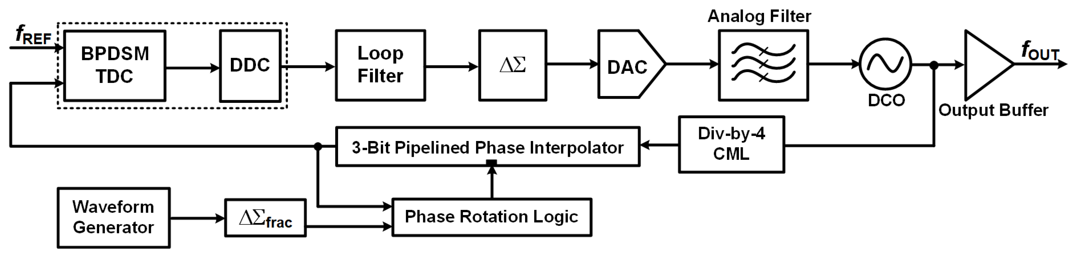
Figure 2.
The discrete-time phase-domain model of the proposed.
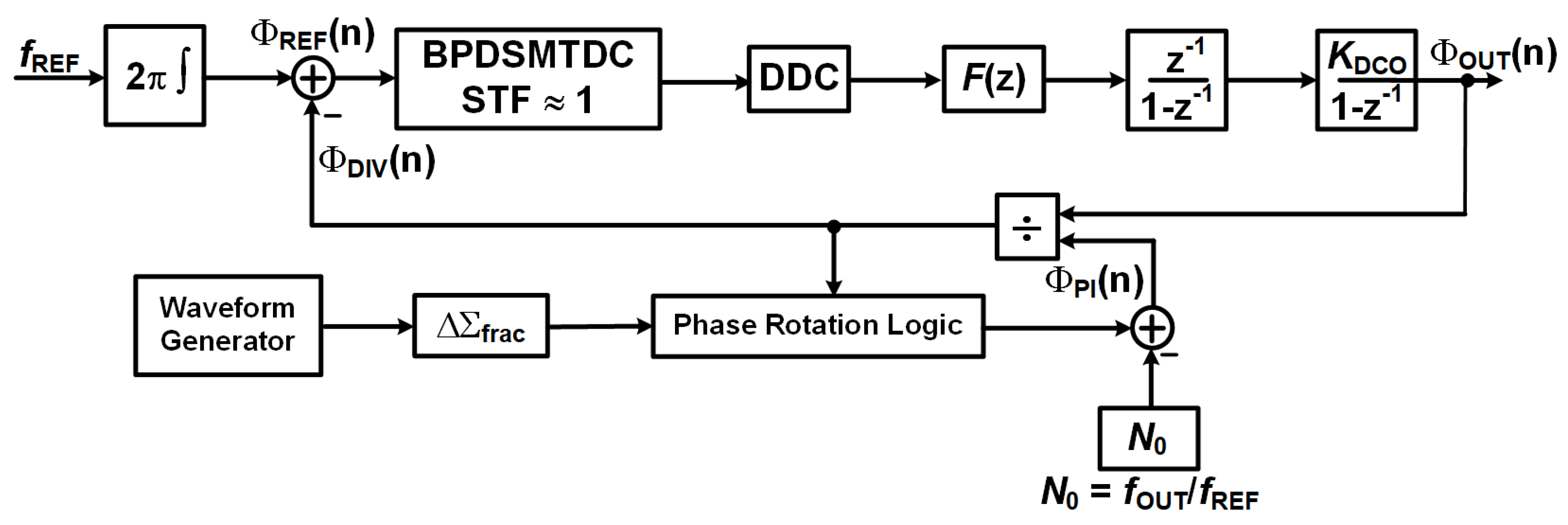
Figure 3.
Block-level circuit implementation of the proposed band-pass delta-sigma TDC.
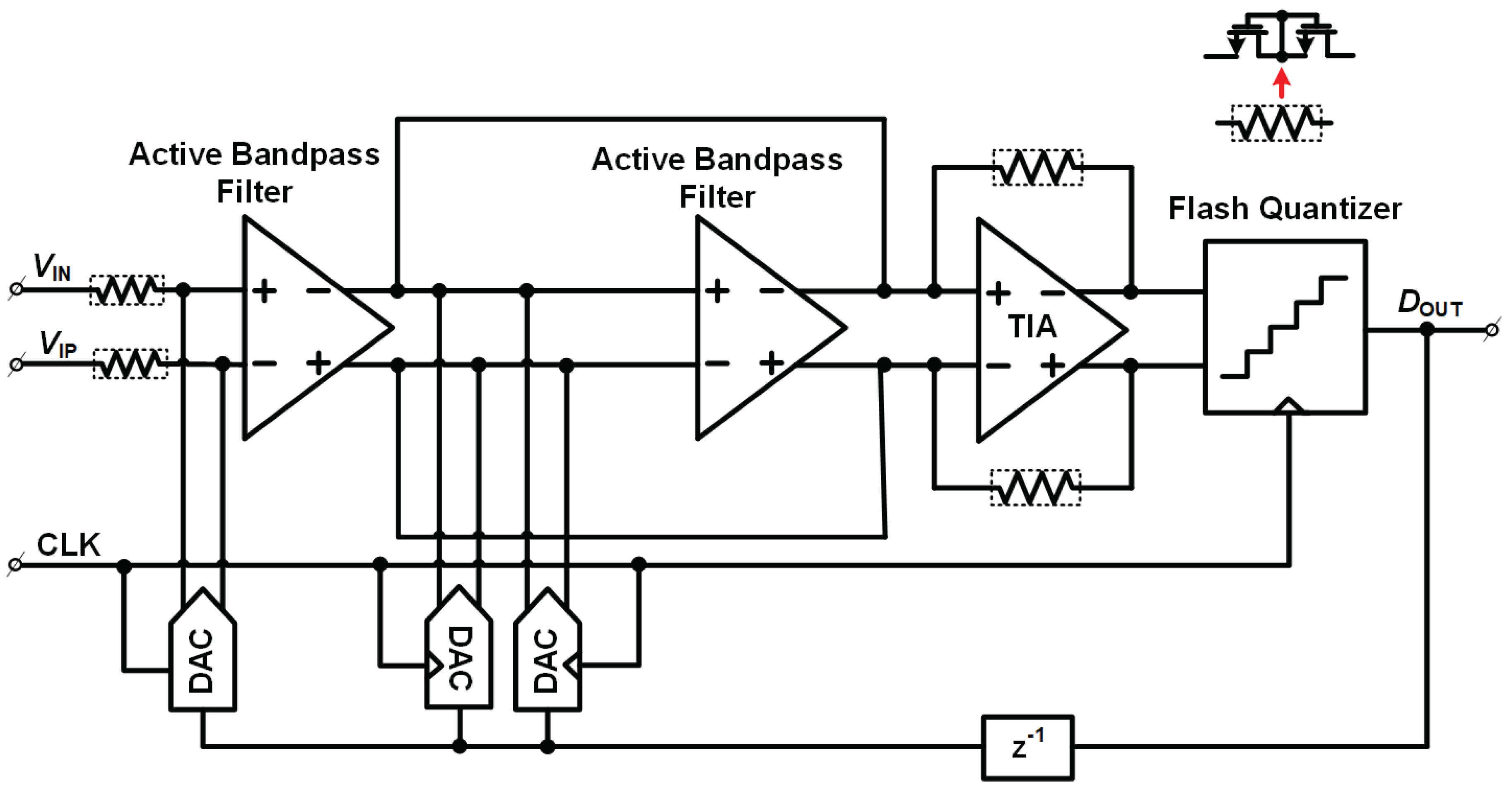
Figure 4.
Circuit schematic of the active band-pass filter (a), Transistor-level implementation of the transimpedance amplifier (TIA) (b), Multi-bit flash quantizer with thermometer-to-binary encoding(c).
Figure 4.
Circuit schematic of the active band-pass filter (a), Transistor-level implementation of the transimpedance amplifier (TIA) (b), Multi-bit flash quantizer with thermometer-to-binary encoding(c).
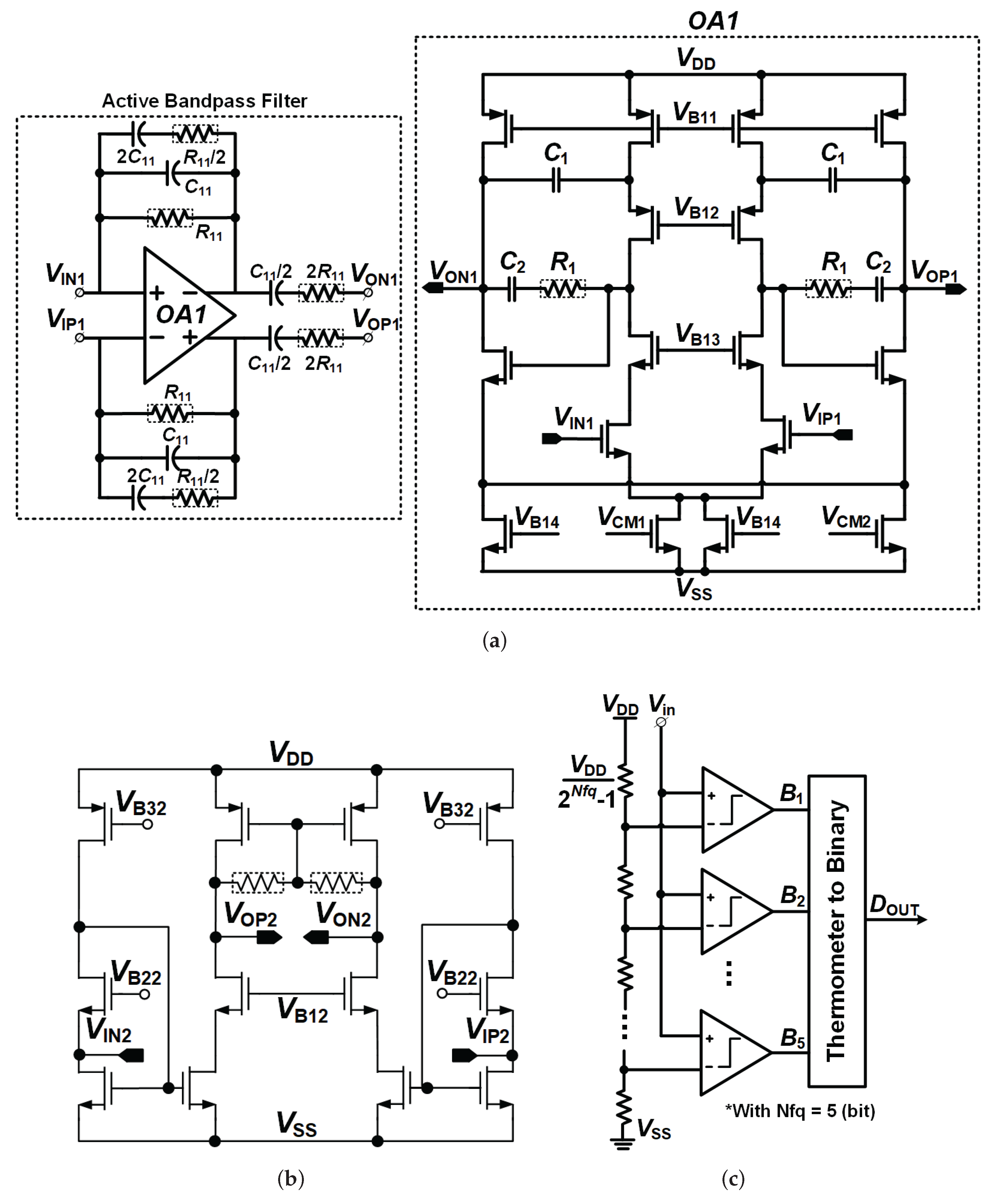
Figure 5.
The proposed oscillator.
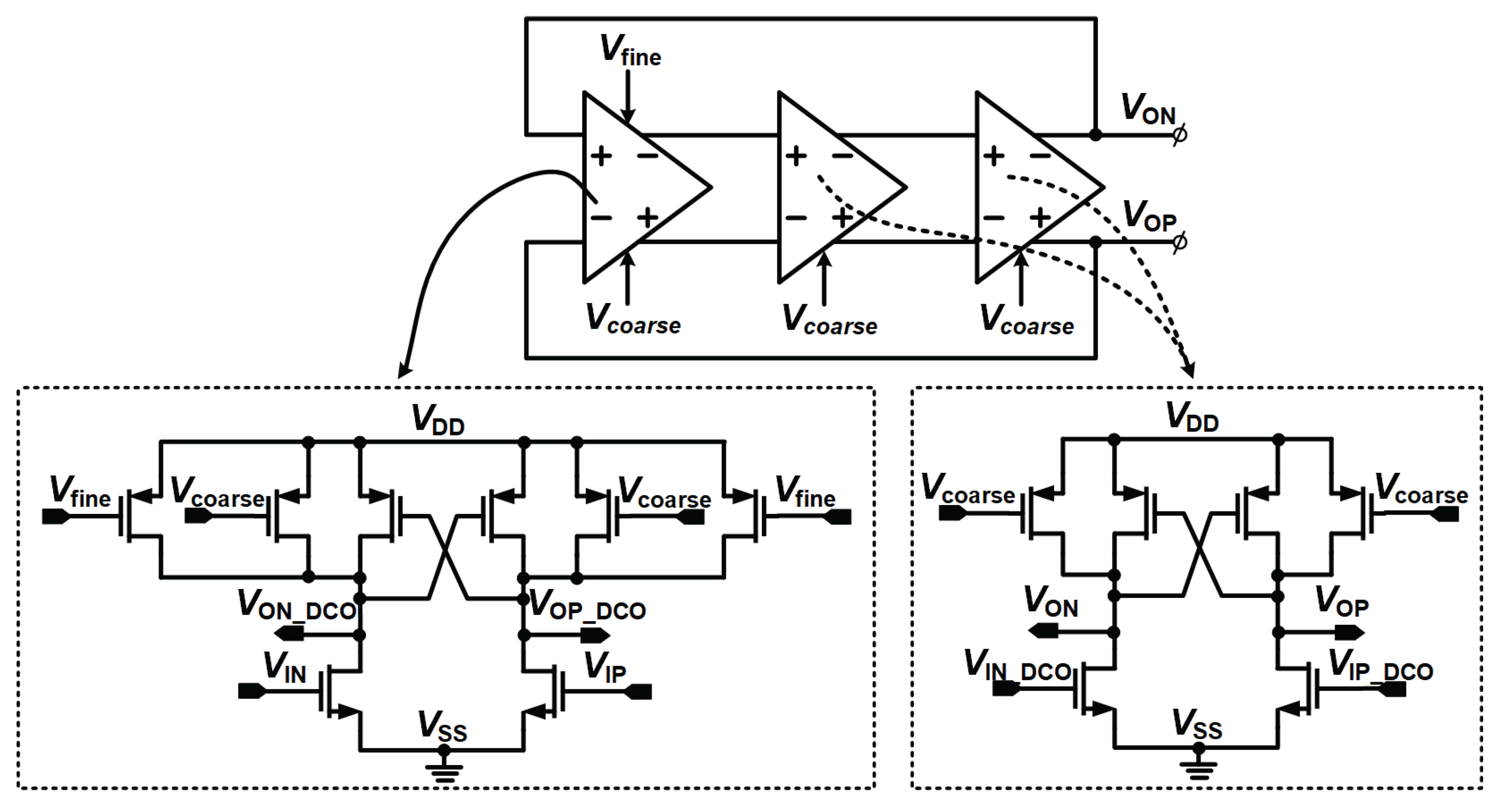
Figure 6.
CML Divider (a), Schematic of Div-by-2 (b), CML Latch(c).
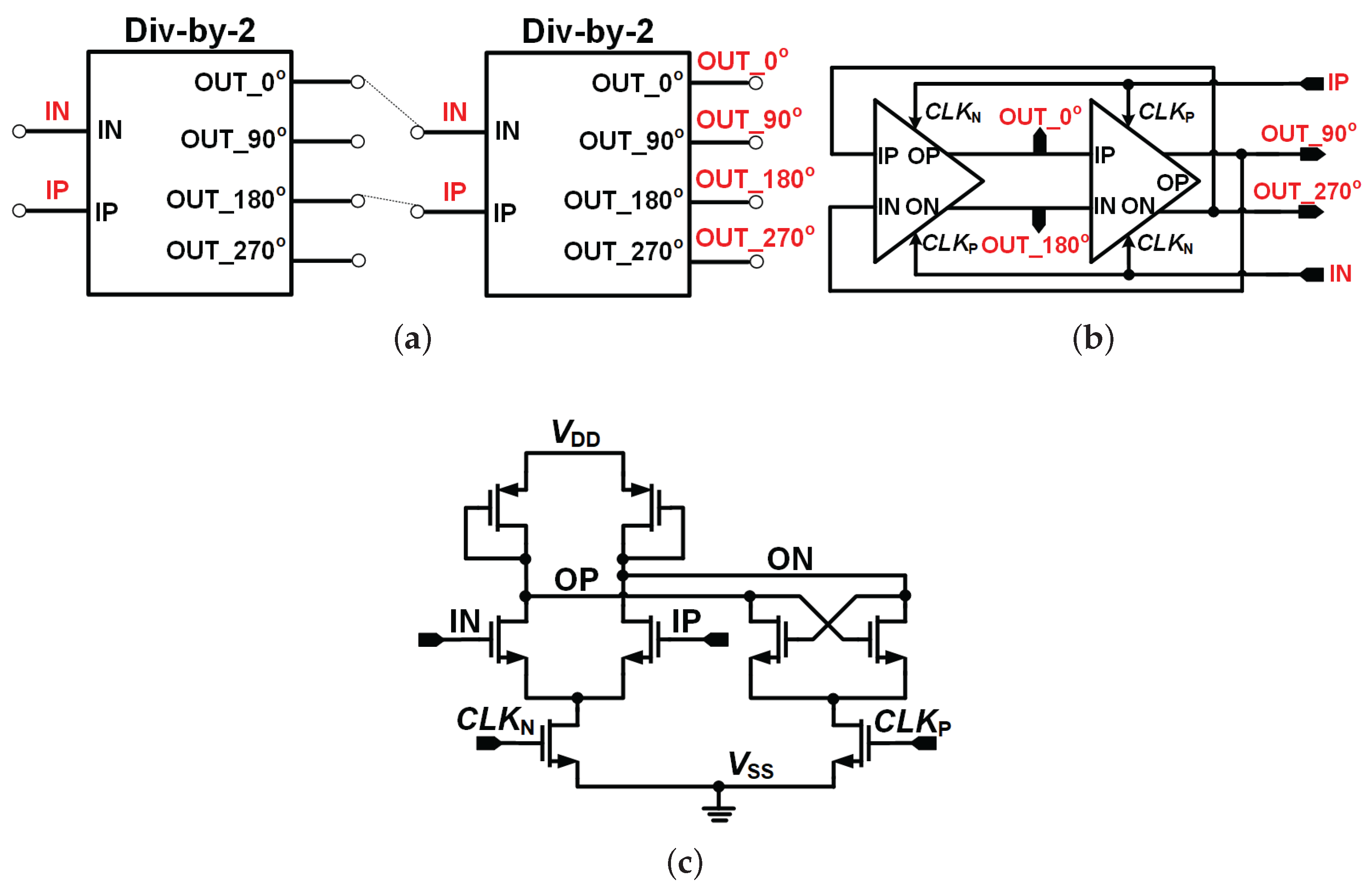
Figure 7.
Pipelined phase interpolator.
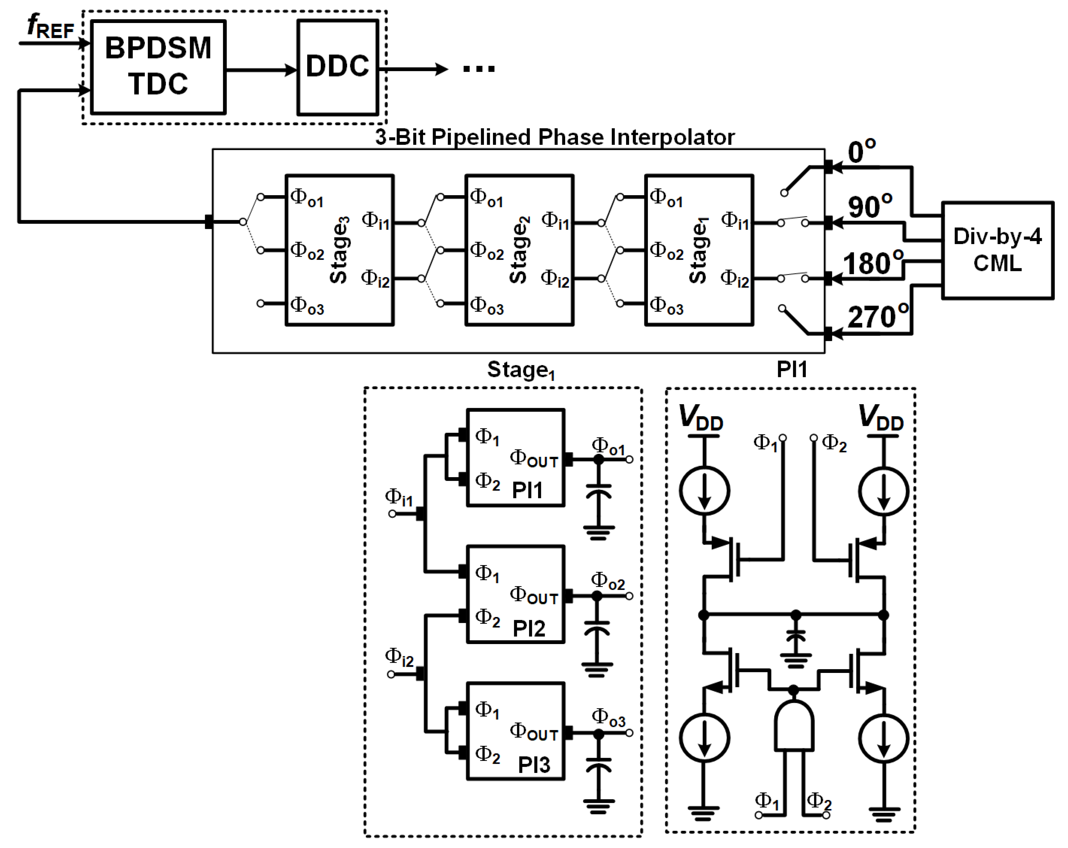
Figure 8.
Die micrograph.
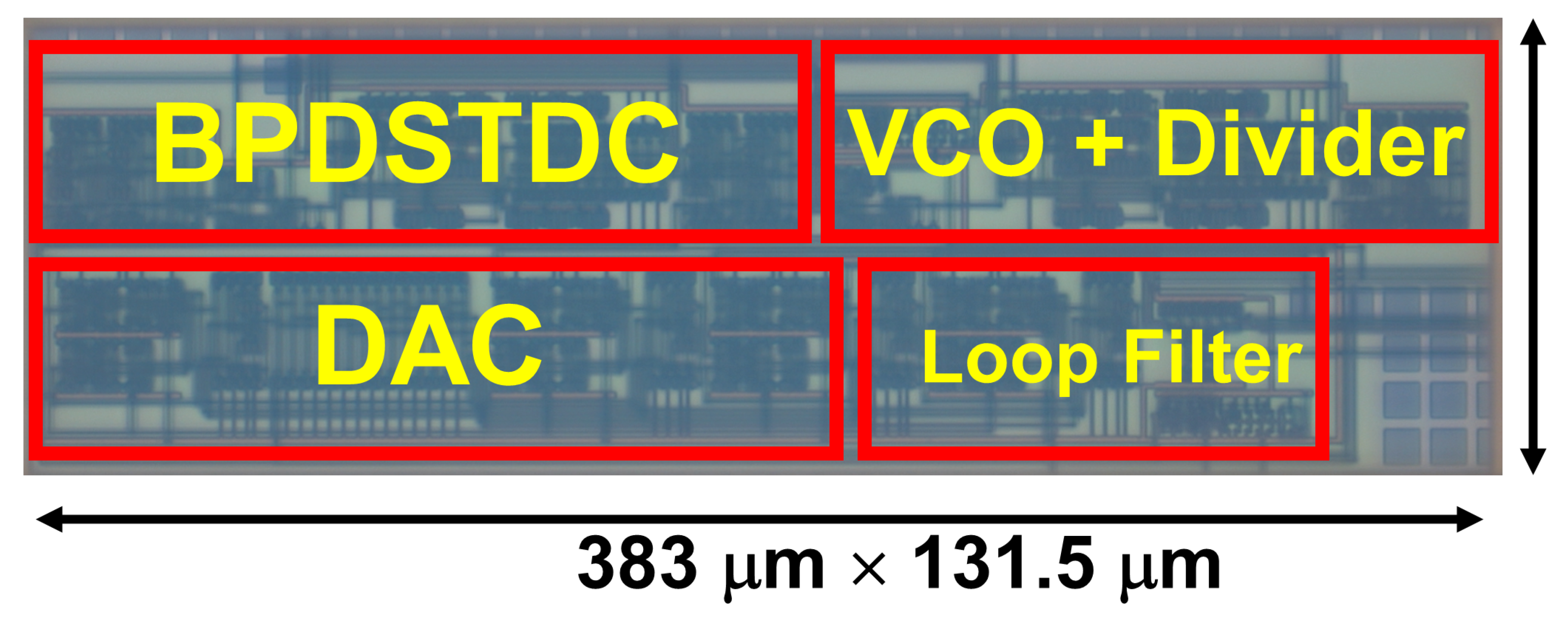
Figure 9.
BPDSM output spectrum at =100 MHz
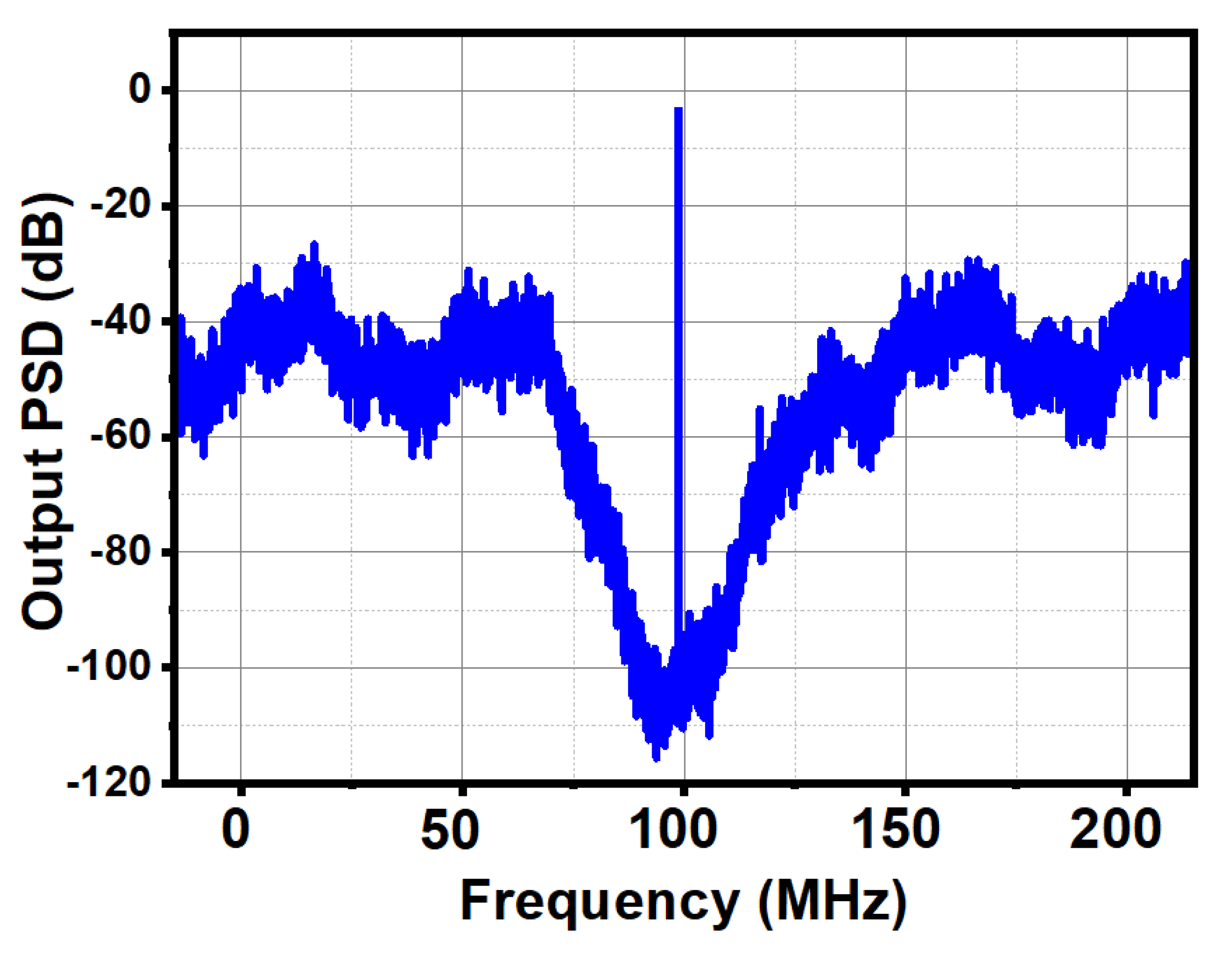
Figure 10.
Output spectrum at 3.2 GHz.
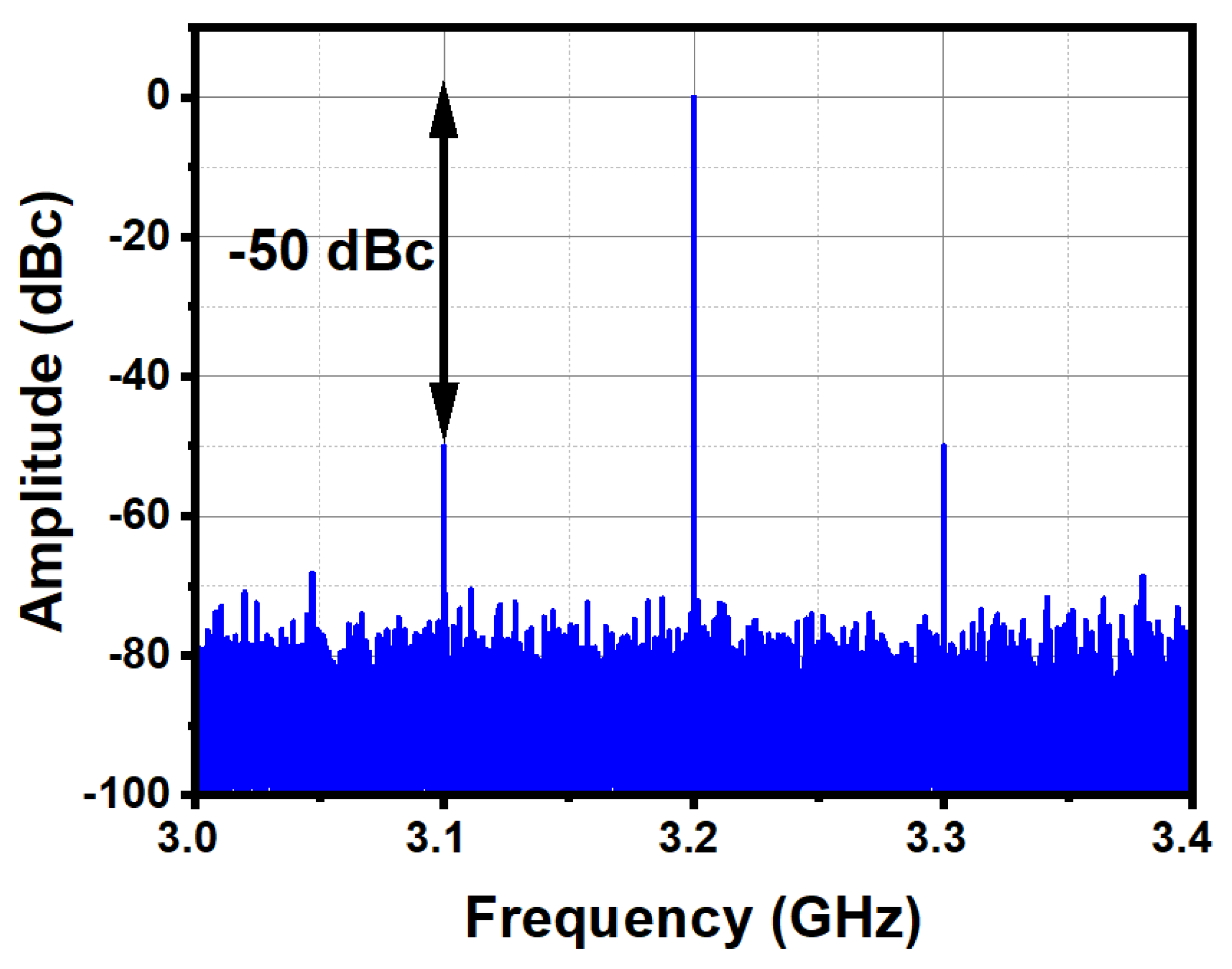
Figure 11.
PLL output spectrum with measured phase noise .
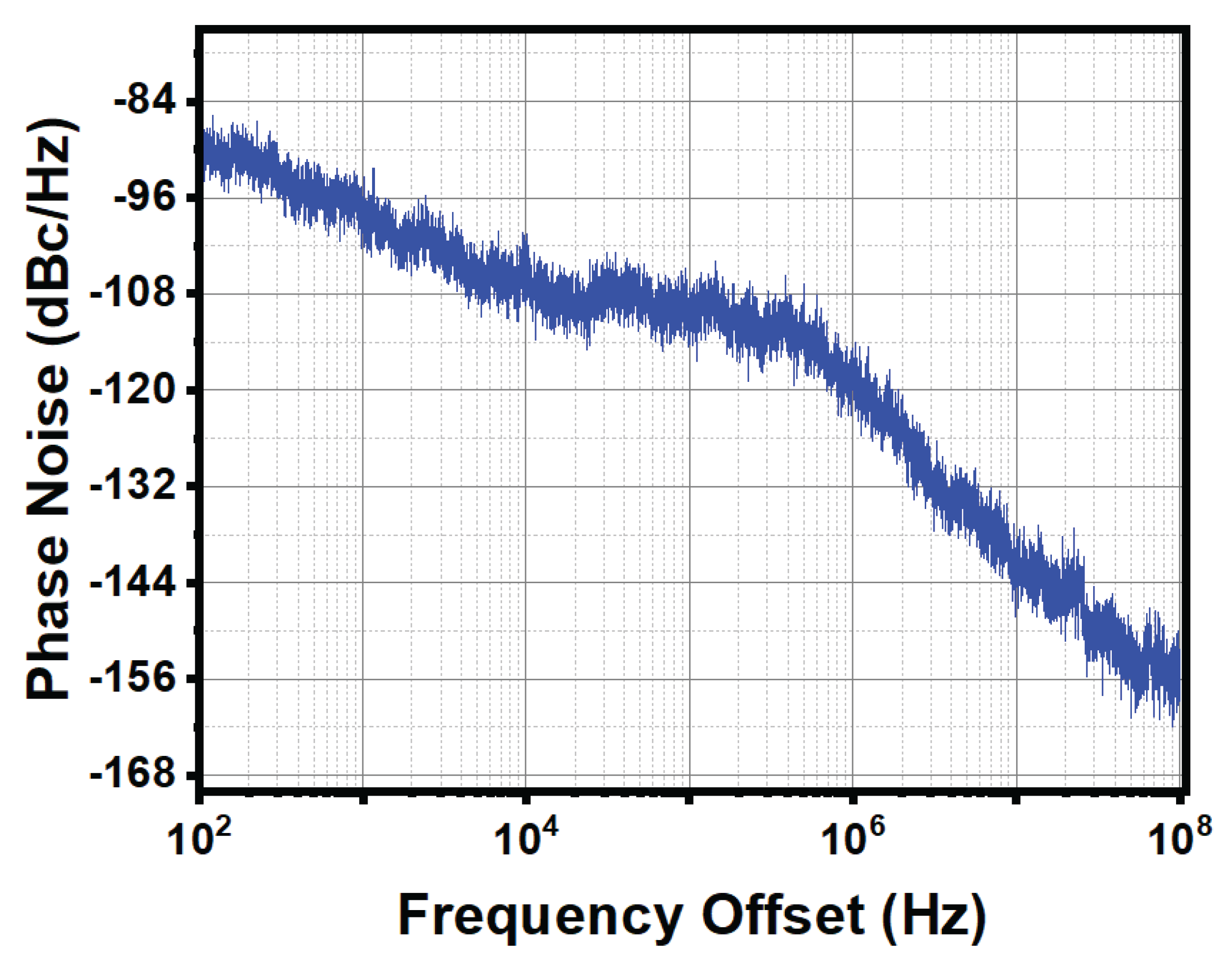

Table 1.
Comparison Table.
| Ref | [25] | [26] | [27] | This work |
|---|---|---|---|---|
| Tech. (nm) | 65 | 28 | 40 | 180 |
| Architecture | ADPLL | BBPLL | ADPLL | ADPLL |
| Ref. Freq (MHz) | 26×2 | 250 | 40 | 50 |
| Out. Freq (GHz) | 2 - 2.6 | 8.5 - 10 | 2.56 - 4.1 | 18.4 - 20.6 |
| FOM* (dB) | -246 | -250.3 | -249.4 | -240 |
| Ref. Spur (dBc) | -72 | -70.2 | 0.043 | -56 |
| Phase Noise (dBc/Hz) | -112.2 | -120.2 | -119.76 | -136 |
| Power (mW) | 0.98 | 20 | 3.48 | 3.1 |
| Area (mm2) | 0.23 | 0.23 | 0.31 | 0.0012 |
Scaled to 28 nm process following [28].
Disclaimer/Publisher’s Note: The statements, opinions and data contained in all publications are solely those of the individual author(s) and contributor(s) and not of MDPI and/or the editor(s). MDPI and/or the editor(s) disclaim responsibility for any injury to people or property resulting from any ideas, methods, instructions or products referred to in the content. |
© 2026 by the authors. Licensee MDPI, Basel, Switzerland. This article is an open access article distributed under the terms and conditions of the Creative Commons Attribution (CC BY) license (http://creativecommons.org/licenses/by/4.0/).
Copyright: This open access article is published under a Creative Commons CC BY 4.0 license, which permit the free download, distribution, and reuse, provided that the author and preprint are cited in any reuse.


