Submitted:
07 January 2026
Posted:
08 January 2026
You are already at the latest version
Abstract
All-inorganic metal halide perovskites exhibit excellent morphology-dependent pho-tophysical properties. Thus, detailed knowledge of photophysical behavior and mor-phological dependence of CsPbBr3 crystals is crucial for device engineering. However, the inability to directly control the morphology of CsPbBr3 crystals arises from a lim-ited understanding of their crystallization mechanism. Herein, we varied the prepara-tion parameters to investigate the perovskite growth mechanism and the impact of these parameters on size and shape of CsPbBr3 single crystals. By optimizing the solu-tion processing, the shape was tuned from the typical cubic microcrystals to more ir-regular ones. We have shown that three main factors favor the growth and formation of CsPbBr3 microcubes, namely high precursor concentration, high temperature and the use of DMSO solvent. The crystal size and density can be tuned by adjusting the precursor concentration, heating temperature, heating time and drop volume. The ob-tained crystals were of high quality and exhibited a strong photoluminescence at room temperature. This work not only introduces a distinct new morphology within the CsPbBr3 microcrystals family but also provides a fundamental understanding of the growth mechanism of these newly emerging functional materials.
Keywords:
growth mechanism
; microcrystal
; solution processing
; size control
; morphology
1. Introduction
All inorganic metal halide perovskites (CsPbX3; X=Cl, Br or I) represent a fascinating class of materials with a wide range of properties that depend on their composition [1]. In particular, CsPbBr3 has been proposed recently as promising candidate because of its enhanced stability and outstanding electronic properties compared to its organic counterparts [2]. This ternary compound has been used in a variety of applications such as solar cells [3], lasers, light emitting diodes [4] and photodetectors [5]. However, the overwhelming majority of perovskite devices are based on CsPbBr3 polycrystalline thin films, which suffer immensely from a high density of traps and grain boundaries [6]. Compared with the polycrystalline thin films, CsPbBr3 single crystals display exceptionally low trap density [7]. For growing single CsPbBr3 crystals, solution processing methods [7,8,9] have emerged among the best techniques, because of the low temperature involved, the low cost and the easy scalability to industry manufacture. Understanding the growth mechanism of single crystals is one of the most important issues in profiling perovskite-based device problems. It is known that the morphology of perovskite nanocrystals (NCs) is controlled by adjusting growth conditions such as the concentration of precursors, the reaction temperature and time, as well as the precursor solution aging and annealing time [10,11,12,13,14]. Nevertheless, additional extensive experimental investigations are still needed to gain a full understanding of the growth mechanism of CsPbBr3 single crystals, and for predicting their morphology. The impact of the growth parameters on the shape, size and surface properties still remains poorly understood, which calls for more detailed studies of both structure and morphology. Herein, we have varied the preparation parameters during the drop casting to investigate the perovskite growth mechanism and the impact of the selected parameters on the size, morphology and photoluminescence of CsPbBr3 perovskite single crystals. Different microcrystal morphologies were obtained which all exhibited high quality and strong green photoluminescence at room temperature. These findings pave the way for future control of the crystallization process of perovskites, which is essential to advance the performance of advanced optoelectronic devices.
2. Materials and Methods
2.1. Crystals Preparation
The precursor solutions were characterized for the precursors size by dynamic light scattering (DLS), carried out on a Zetasizer Nano (Malvern Instruments, UK), using disposable polystyrene cuvettes. For each sample, 15 different distribution plots were obtained by sequential measurements, and averaged. After that, the solutions were cast with a micropipette onto substrates (silicon wafer, ITO coated glass, gold), which had been previously cut into pieces of approximately 1 cm x 1 cm size. All chemicals and materials were acquired from Sigma Aldrich (St. Louis, MO, USA). ITO-coated glass wafers to be used as substrates were rinsed sequentially with absolute ethanol and acetone in an ultra-sonicator bath. The cleaned wafers were hydroxylated via Piranha treatment at room temperature (RT) for 20 min and with H2O2/H2SO4 (3:7) at 60°C, then rinsed with water and dried with argon flux. Finally, the substrates were rinsed with toluene and deionized water and then dried in a nitrogen stream.
Whereas the silicon substrate was not highly-doped, and the native oxide on top was not removed with hydrofluoric acid bath, still the overall behavior in the SEM (see below) was such that electrical conductivity under high energy electrons in the beam was ensured. Drying on the hotplate was inspected visually during the process.

Table 1.
Summary of the growth parameters of CsPbBr3 crystals.
| Sample ID | Precursor concentration (M) | Drop volume (mL) | Heating time (min) | Heating temperature (°C) | Solvent | Substrate |
| D1 | 0.3 | 10 | 5 | 150 | DMSO | ITO/glass |
| D2 | 0.2 | 10 | 5 | 150 | DMSO | ITO/glass |
| D3 | 0.3 | 2.5 | 5 | 150 | DMSO | Gold |
| D4 | 0.3 | 2.5 | 1 | 150 | DMSO | Gold |
| D5 | 0.3 | 2.5 | 0.5 | 150 | DMSO | Gold |
| D6 | 0.3 | 10 | 5 | 90 | DMSO | ITO/glass |
| D7 | 0.3 | 10 | 5 | 120 | DMSO | ITO/glass |
| D8 | 0.3 | 10 | 5 | 150 | DMF | ITO/glass |
2.2. Crystals Characterization
2.2.1. SEM (Scanning Electron Microscopy)
The SEM imaging was carried out using a HRSEM JEOL JSM-7500LA (JEOL, Tokyo, Japan) equipped with a cold field-emission gun, operating at 25 kV acceleration voltage. No additional conductive coating was needed.
2.2.2. AFM (Atomic Force Microscopy)
The AFM measurements were carried out using a XE 100 (Park Systems, Korea) microscope under ambient atmosphere, using 25Pt300B probe tips from Rocky Mountain Nanotechnologies (USA).
2.2.3. Optical Microscopy Analysis
Optical images were obtained with a confocal zeta-20 profilometer (Zeta instruments, USA) and with an Olympus stereomicroscope (24×). The movies were recorded with a CCD camera from Thorlabs connected to an optical mono-zoom (12×) at maximum magnification (24×).
2.2.4. XRD (X-Ray Diffraction Spectroscopy)
The XRD measurements were carried out using a Panalytical Empyrean X-ray diffractometer equipped with 1.8 kW CuKα ceramic X-ray tube PIXce3D 2x2 area detector and operating at 45 kV and 40 mA. XRD data analysis was performed using high Score 4.1 software.
2.2.5. Confocal Microscopy
Confocal photoluminescence (PL) microscopy was used to obtain emission images and to acquire spectrum of individual microcrystals under 488 nm wavelength (blue light) excitation, with collection in the cyan-green window (500-550 nm).
3. Results and Discussion
3.1 Properties of the Crystals
In Figure 1a,b SEM micrographs of different regions of sample D1 are shown. In most of the sample area, only the typical nearly cubic CsPbBr3 microcrystals appears (see Figure 1a), but occasionally other morphologies are seen between the microcubes, such as irregular polygons, crosses or even needles (see Figure 1.b).
In our previous work [15,16], we focused only on the microcube-like shape. As shown in Figure 1c,d, the microcubes feature a pyramidal cavity on the top surface of the crystal and this cavity changes from one crystal to another crystal in the same sample. However, the irregular polygonal crystals apparently do not exhibit this cavity (see Figure 1e). The AFM images show a similar tendency in good agreement with the SEM results in cavity form in microcubes (see Figure S1). Strong green emission was observed from PL map acquired under laser excitation with 488 nm wavelength in a confocal microscope, confirming the crystalline nature of the sample. The microcubes crystallize in orthorhombic structure, as illustrated by the diffractogram shown in Figure 1f. We should mention that the crystalline phase remains the same by using different substrates (Figure S2). From higher magnification images (Figure 1g,h), the appearance of cross-like branched crystals is even more clear than in Figure 1b. In general, these crystals grow around the individual microcubes, or in the space between them. Optical micrographs in Figure S3 confirm this growth tendency. Interestingly, the cross-branched crystals also exhibit strong green emission, as revealed by the PL map in Figure 1i.
Controlled growth of branched crystals was originally reported several decades ago for zinc oxide (ZnO) [17,18] and more recently for indium Phosphide (InP) [19]. In colloidal systems, ensembles of centrally branched Cadmium Telluride (CdTe) NCs have been prepared with a high degree of control over the branch length and diameter [20]. From our AFM images, we determined the three-dimensional (3D) topography of the obtained branched crystals (see Figure 2a,b).
In Figure S4, the presence of two (or three and even four) microcubes merged into a single entity is clearly observed. These features are characteristic of crystal coalescence, predominantly occurring via an oriented attachment mechanism or a closely related intergrowth process. This coalescence is driven by the high surface energy of exposed crystallographic facets and accelerated growth kinetics, which favor the alignment and fusion of neighboring microcubes. Consequently, larger microcrystals containing internal grain boundaries are formed. Such a process is widely recognized as a key pathway for microstructure development through the assembly of perovskite nanocrystals, and developed by various groups [21,22]. Here is shown that similar phenomenon can be observed in microcrystals and growth control can lead even to the assembly of perovskite microcubes.
To gain better insight about the origin of the structures observed in sample D1, we optically monitored the growth process of D1 and the corresponding video clips are provided as supplementary material. Figure S5 shows the photographs taken at different times during the reaction process. The growth of CsPbBr3 crystals is divided in two phases: During the first phase the DMSO solvent was abundant and large cuboid crystals were formed. During the second phase, the DMSO evaporated rapidly upon heating leading to a larger area covered by branched and anisotropic CsPbBr3 crystals, and a high-speed surface growth was observed. Thus, the growth of CsPbBr3 crystals must have occurred under supersaturation conditions [23] of dissolving precursor, in DMSO solvent. In fact, by using drop casting method for deposition, it is known that supersaturation can be achieved through evaporation of DMSO solvent [24].
The growth velocity normal to the surface, vn, is known to behave as follows [24,25]:
vn ∝ σ vkin ΔC ,
Where σ is a condensation coefficient or attachment kinetics coefficient, vkin is a thermal movement factor, and the last term in the product is the difference between the actual precursor concentration in solvent Csol and the saturation concentration at the surface of the crystals Csat, namely ΔC=(Csol−Csat). When the organic solvent was abundant, ΔC was very small, meaning that crystal growth is largely governed by attachment kinetics, i.e. σ. Under these conditions, we believe that the growth process corresponded to the “diffusion- limited regime”. In this regime, CsPbBr3 cubic crystals were grown slowly, and large crystals were formed. However, when the solvent was rapidly evaporated under heating, ΔC became more significant. In this case, the growth process was “attachment kinetics limited” regime, where the precursors diffused rapidly to the crystal surface. As a result, branched and anisotropic crystals were formed.
The morphology of CsPbBr3 single crystals obviously depends on the growth mechanism. Controlling the growth conditions is therefore likely the key factor to understand the crystallization process of the obtained crystal morphologies. Hence, we carried out additional experiments to investigate the influence of the following preparation parameters: precursor solution concentration, drop volume, heating time, heating temperature and solvent type.
First, the effect of precursor concentration was studied. By using relatively high concentration (0.3 M), the dominating crystal morphology was that of microcubes with edge size ranging from 20 µm to 80 µm (see Figure 3a,b). When the concentration was decreased to 0.2 M, rounded structures with diameters around 2 µm were formed (see Figure 3d,e). Importantly, with decreasing concentration the surface became almost completely covered.
By using ImageJ, we calculated the percentage of substrate area occupied by crystals. Sample D1 exhibits the lowest surface coverage (14%) compared to D2 (77%), indicating a sparse distribution of crystals with large uncovered regions, while increased coverage in D2 suggests enhanced nucleation density and more homogeneous crystal distribution.
In addition, we noted the presence of some square-shaped crystals (Figure 1e and Figure S6). Notably, this finding indicates that relatively precursor’s high concentration favors the growth of microcubes. Interestingly, the comparison of the PL map recorded from sample D1 (Figure 3c) with that of D2 (Figure 3f) shows that the emission of single microcubes is higher than that of rounded microcrystals. Therefore, we can conclude that even when the surface is quasi-covered, the emission from microcubes is significantly stronger than that of rounded ones. Du et al. [26] have investigated the influence of precursor concentration on the morphology, crystallinity and optical properties of perovskite thin films. They found that the grain size increases with increasing precursor concentration. This demonstrates that a higher precursor concentration is favorable to grain growth. As the precursor concentration increases, the supersaturation level also increases, leading to the formation of larger nuclei. With the annealing process, the grains begin to grow and become larger due to the higher supersaturation [26].
Next, we examined the impact of the drop volume V. Analysis of micrographs acquired from samples D1 and D3 revealed a decrease in microcube size and an increase in crystal density with the increase of V, (sample D3 shows improved surface coverage of 41% compared to 14% of D1). Specifically, the crystal edge length increased from ~12 µm to ~65 µm when V was increased from 2.5 µL to 10 µL. Additional optical micrographs can be found in Figure S6. Similar morphologies were observed in sample D3 (see AFM images in Figure 2). Furthermore, photoluminescence mapping conducted on samples D3 and D1 revealed at microcubes formed with V=10 µL displayed stronger emission compared to those formed with V=2.5 µL.
Riet et al. [27] have investigated the influence of crystal morphology on the photoluminescence properties of MAPbBr3 thin films, and they found that the PL intensity and lifetimes were significantly smaller in films with micrometer-sized crystallites compared to granular films and this because of different size of the crystals morphologies. In our work, larger cubic crystals exhibited enhanced PL properties compared to smoother, rounded and smaller ones. Overall, these results suggest that achieving a high density of large crystals holds great promise for practical optoelectronic applications.
Through our testing of heating time, we discovered that a certain duration is required for the solvent to evaporate. Figure 4 displays optical micrographs taken at various heating durations. The results indicate that as the heating time increases from 30 s to 5 min, there is a tendency for the crystal size to increase (mean shifts from ~4 µm at 30 s – Figure 4e,f - to ~12 µm at 1 min – Figure 4c,d - onto ~20 µm at 5 min Figure 4a,b) and the surface coverage to decrease (from ~66% to ~44% onto ~51%, respectively). With further increasing the heating time, emergence of additional morphologies on the surface appears. Therefore, we can conclude that prolonging heating times results in increased size and promotes the growth of diverse morphologies on the substrate surface (branched and anisotropic crystals).
We also investigated the effect of heating temperature on the growth of CsPbBr3 crystals. The images of the whole deposited drop are presented in Figure S7. As shown in Figure 5, increasing the heating temperature from 90°C to 150°C led to the formation of well-defined microcube shaped crystal. Notably, the edge length of single crystal increased from approximately 40 µm to 150 µm as the temperature arose from 90°C to 150°C, while the overall crystal density decreased. This growth behavior can be attributed to changes in supersaturation state of precursor solution.
At lower temperatures, higher supersaturation levels promoted rapid nucleation resulting in a high density of smaller cubic crystals. In contrast, at elevated temperatures the reduced supersaturation suppressed nucleation rates and favored crystal growth over nucleation. As a result, fewer nuclei formed but they grew into larger crystals. This regime facilitated the development of larger and more uniform microcubes. This finding underscores the critical role of the heating temperature in modulating both nucleation kinetics and grain size during the growth of CsPbBr3 perovskite crystals.
In this part, we tested the solvent effect on the crystallization process of our crystals. According to previous reports, the fabrication of perovskite materials via solution processing typically involves dissolving the raw materials in polar solvents such as N,N-dimethylformamide (DMF), dimethyl sulfoxide (DMSO), γ-butyrolactone (GBL), or mixtures thereof [28]. Figure 6a,d show comparative micrographs of samples D1 and D8. When using solvent of different polarity, the morphologies evolved from large cubic crystals with DMSO to small ones with DMF. The edge lengths of the resulting microcrystals ranged from 10 µm to 45 µm (mean edge size ).
High-magnification images (Figure 6.b,c and e,f) reveal that the microcrystals formed in DMF possess a distinct top surface, which is neither flat nor features the inverted pyramidal cavities observed in Figure 6.b,c. The solvent solute-interactions driven by the Lewis acid-base reaction facilitated the dissolution of perovskite reactants (precursors) and, more importantly, allowed the perovskite crystallization process to be controlled by carefully coupling Pb2+ with Lewis bases that have different degree of basicity. The organic solvents used in the solution process such as DMSO, DMF or GBL, act as Lewis bases because they contain donor groups (nitrogen (N)-donor, oxygen (O)-donor and sulfur (S)-donor), while the metal cations (Pb2+, Sn2+) in perovskite precursors act as Lewis acids that accept lone pairs of electrons [29]. The choice of solvent largely affects the properties of the fabricated perovskite thin films, such as grain size, grain orientation, film morphology, and defect density [30]. DMSO has a stronger basicity than DMF and GBL due to its larger Gutmann donor number, and thus coordinates effectively with metal cations [31]. The stronger coordination between DMSO and metal cations stalls the halides in precursor and retards the overall crystallization rate [30] (see Figure 6.g). Moreover, rapid perovskite crystallization results in reduced grain size and an excess of grain boundaries in perovskite films [29]. Thus, prolonging crystallization process by using DMSO enables the growth of larger perovskite grains and improves the perovskite film quality. Therefore, we conclude that the use of DMSO in our work slowed down the crystallization rate and allowed to obtain high density of larger crystals compared to DMF-based crystals.
It is well known that the nature of the solvated species in the precursor solution impacts on the material resulting from them. Numerous studies have attempted to elucidate the relationship between non-stoichiometric precursors and their effects on nucleation and crystal growth processes [25]. To gain further insight, we employed steady-state optical spectroscopy, a straightforward technique to probe lead bromide species in perovskite precursor solutions. Absorbance and photoluminescence (PL) spectra were recorded for a CsBr:PbBr₂ mixture (1.1 molar ratio) dissolved in both DMSO and DMF; the results are shown in Figure 7b.
The DMSO solution exhibited an absorbance peak at 285 nm attributed to PbBr2 [26], whereas the DMF solution showed a similar peak but with reduced intensity. Both solutions presented an absorbance tail in 310-320 nm range, indicating the presence of [PbBr3]- species, consistent with earlier studies [27,28]. Additionally, absorbance tails were observed in the longer wavelength region (340–360 nm), suggesting the possible formation of [PbBr4]2- species [27,28]. Both solutions exhibited PL peaks at 599 nm and 553 nm, corresponding to the emission from [PbBr₃]⁻ and [PbBr₄]²⁻ species, respectively. This aligns with previous literature, where these species are reported to be emissive at approximately 600 nm and 560 nm, respectively.
A better understanding of the composition and particle size in the precursor solution is essential. Methodologies like DLS offer valuable insights into the physicochemical properties of the solution, particularly in relation to solvent choice and specimen size. The DLS data presented in Figure 7c show that the DMSO solutions contained lead bromide species around 1 nm in size, whereas the DMF solution comprised notably larger clusters. Our findings suggest that changing the solvent significantly alters both the speciation and the solvo-dynamic size of the lead bromide species and the resulting crystal morphology.
3.2 Stability of the Crystals
Figure 8 shows optical micrographs of aged samples taken after two months of storage under ambient conditions. The images reveal the presence of crystalline domains on the surface, suggesting that crystals are susceptible to displacement either during measurement or sample handling (see red arrows in Figure 8a,b, and f).
Furthermore, the observed surface features on the crystal surface - including voids and apparent material loss (see Figure 8.c,d and e) - indicate progressive degradation of the crystalline structure over time. This implies limited long-term stability of the material in air. However, in comparison with thin films or nanocrystals, our crystals present better resistivity to air and humidity. As shown in the inset to Figure 8.f, the precursor solution remains very clear (transparent), even after one month. Orange color of precursor solution traduces non-dissolving of the salts solution and/or salts contamination or supersaturated solution. Using an aged precursor solution stored for one day, we obtained the optical micrographs presented in Figures S8.b,c. The images clearly reveal the formation of anisotropic, branched crystal structures, while no cubic crystals were observed. The entire droplet (Figure S8.a) exhibited a uniform branched morphology, indicating significant changes in the crystallization behavior induced by precursor aging. These findings emphasize the crucial role of using freshly prepared solutions to achieve controlled and reproducible crystal growth. Furthermore, the results confirm that samples derived from aged precursor solutions display distinct morphological and possibly structural differences compared to those obtained from fresh solutions.
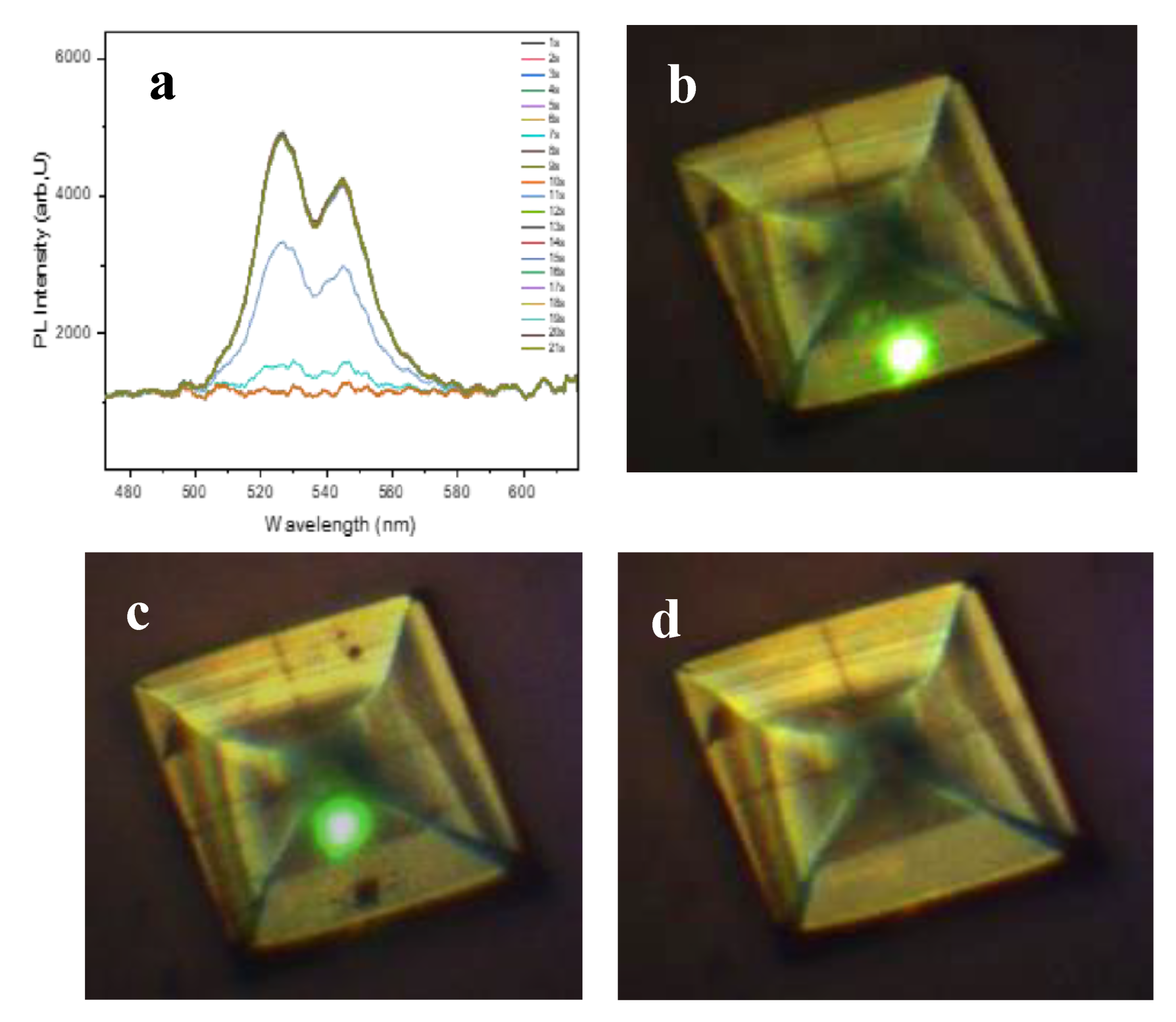
The photostability of our crystals was investigated by performing measurements at different times scales on single crystal by micro-PL setup, and the results are illustrated in Figure 9. While the microcrystal was continuously exposed to the laser, it is important to notice that upon illumination the PL intensity decreased. The samples were exposed to the laser until PL intensity had significantly dropped. This degradation occurred on a longer time scale compared to nanocrystals growth [32]. We also note the appearance of black voids on the surface, indicating the loss of material under illumination (see Figure 9b-d).
The decrease of PL intensity suggests that, on a time scale seconds, the number of charge carriers that recombine non-radiatively increases. According to previous work, illumination of perovskite samples can create trap states [27]. A likely mechanism of these traps states is the formation of lead bromide vacancies [33]. The most favorable ion to move in CsPbBr3 is bromide, since halide anion vacancies present theoretically the lowest activation energies.
4. Conclusion
In summary, by using drop casting method, we obtained different crystal morphologies such as cubic, branched, round and anisotropic structures. We explored several approaches to control the shape, size and density of the crystals. We observed that three key factors favor the formation of cubic CsPbBr3 crystals, namely high precursor concentration, elevated temperature and the use of DMSO as solvent. The crystal size and density can be tuned by adjusting the precursor concentration, heating temperature and duration, and drop volume. The obtained crystals were of high structural quality and exhibited strong green photoluminescence. This work paves the way to control the crystallization process of perovskite materials for the development of optoelectronic devices based on perovskite single crystals.
Supplementary Materials
The following supporting information can be downloaded at the website of this paper posted on Preprints.org.
Author Contributions
Conceptualization, K.A., F.H. and Z.Z.; methodology, K.A. and M.S.; validation, F.H. and Z.Z.; formal analysis, K.A.; investigation, K.A. and M.S.; resources, F.H.; data curation, K.A., M.S. and Z.Z.; writing—original draft preparation, K.A.; writing—review and editing, M.S., F.H and Z.Z.; visualization, K.A. and M.S.; supervision, F.H and Z.Z.; project administration, Z.Z.; funding acquisition, F.H. All authors have read and agreed to the published version of the manuscript.
Data Availability Statement
Data are available on request to the authors.
Acknowledgments
Authors would like to thank the University of Monastir for the financial support of this work. We gratefully knowledge the Italian Institute of Technology for kindly providing the measurement facilities and Roman Krahne for the supervision during the stay of K.A. in iit and for useful discussion.
Conflicts of Interest
The authors declare no conflicts of interest.
Abbreviations
The following abbreviations are used in this manuscript:
| MDPI | Multidisciplinary Digital Publishing Institute |
| DOAJ | Directory of open access journals |
| IGDORE | Institute for Globally Distributed Open Research and Education |
| DMSO | dimethyl sulfoxide |
| NC | Nanocrystals |
| DLS | Dynamic light scattering |
| UK | United Kingdom |
| ITO | Indium-Tin oxide |
| USA | United States of America |
| RT | Room temperature |
| SEM | Scanning electron microscopy |
| DMF | N,N-dimethylformamide |
| AFM | Atomic force microscopy |
| CCD | Charge-coupled device |
| XRD | X-ray diffraction |
| PL | Photoluminescence |
| GBL | γ-butyrolactone |
References
- Protesescu, L.; Yakunin, S.; Bodnarchuk, M.I.; Krieg, F.; Caputo, R.; Hendon, C.H.; Yang, R.X.; Walsh, A.; Kovalenko, M. V. Nanocrystals of Cesium Lead Halide Perovskites (CsPbX3, X = Cl, Br, and I): Novel Optoelectronic Materials Showing Bright Emission with Wide Color Gamut. Nano Letters 2015, 15, 3692–3696. [Google Scholar] [CrossRef]
- Yu, B.; Tan, S.; Li, D.; Meng, Q. The Stability of Inorganic Perovskite Solar Cells: From Materials to Devices. Materials Futures 2023, 2, 32101. [Google Scholar] [CrossRef]
- Tong, G.; Ono, L.K.; Qi, Y. Recent Progress of All-Bromide Inorganic Perovskite Solar Cells. Energy Technology 2020, 8. [Google Scholar] [CrossRef]
- Li, X.; Wu, Y.; Zhang, S.; Cai, B.; Gu, Y.; Song, J.; Zeng, H. CsPbX3 Quantum Dots for Lighting and Displays: Roomerature Synthesis, Photoluminescence Superiorities, Underlying Origins and White Light-Emitting Diodes. Advanced Functional Materials 2016, 26, 2435–2445. [Google Scholar] [CrossRef]
- Li, Y.; Shi, Z.F.; Li, S.; Lei, L.Z.; Ji, H.F.; Wu, D.; Xu, T.T.; Tian, Y.T.; Li, X.J. High-Performance Perovskite Photodetectors Based on Solution-Processed All-Inorganic CsPbBr3 Thin Films. Journal of Materials Chemistry C 2017, 5, 8355–8360. [Google Scholar] [CrossRef]
- Li, J.; Xia, R.; Qi, W.; Zhou, X.; Cheng, J.; Chen, Y.; Hou, G. Encapsulation of Perovskite Solar Cells for Enhanced Stability : Structures, Materials and Characterization. [CrossRef]
- Yu, J.; Liu, G.; Chen, C.; Li, Y.; Xu, M.; Wang, T.; Zhao, G.; Zhang, L. Perovskite CsPbBr3 Crystals: Growth and Applications. Journal of Materials Chemistry C 2020, 8, 6326–6341. [Google Scholar] [CrossRef]
- Xing, G.; Mathews, N.; Lim, S.S.; Yantara, N.; Liu, X.; Sabba, D.; Grätzel, M.; Mhaisalkar, S.; Sum, T.C. Low-Temperature Solution-Processed Wavelength-Tunable Perovskites for Lasing; 2014; pp. 1–5. [Google Scholar] [CrossRef]
- Rakita, Y.; Kedem, N.; Gupta, S.; Sadhanala, A.; Kalchenko, V.; Böhm, M.L.; Kulbak, M.; Friend, R.H.; Cahen, D.; Hodes, G. Low-Temperature Solution-Grown CsPbBr3 Single Crystals and Their Characterization. Crystal Growth and Design 2016, 16, 5717–5725. [Google Scholar] [CrossRef]
- Bealing, C.R.; Baumgardner, W.J.; Choi, J.J.; Hanrath, T.; Hennig, R.G. Predicting Nanocrystal Shape through Consideration of Surface-Ligand Interactions. ACS Nano 2012, 6, 2118–2127. [Google Scholar] [CrossRef]
- Cui, J.; Xu, F.; Dong, Q.; Jia, J.; Liu, L.; Liu, S.; Yang, F.; Ye, X. Facile, Low-Cost, and Large-Scale Synthesis of CsPbBr3 Nanorods at Room-Temperature with 86 % Photoluminescence Quantum Yield. Materials Research Bulletin 2020, 124, 110731. [Google Scholar] [CrossRef]
- Phys, J.A. Progress and Perspective on CsPbX 3 Nanocrystals for Light Emitting Diodes and Solar Cells Progress and Perspective on CsPbX 3 Nanocrystals for Light Emitting Diodes and Solar Cells. 2020, 050903. [Google Scholar] [CrossRef]
- de Weerd, C.; Gregorkiewicz, T.; Gomez, L. All-Inorganic Perovskite Nanocrystals: Microscopy Insights in Structure and Optical Properties. Advanced Optical Materials 2018, 6, 1–13. [Google Scholar] [CrossRef]
- Sun, Q.; Ni, C.; Yu, Y.; Attique, S.; Wei, S.; Ci, Z.; Wang, J.; Yang, S. Design Principle of All-Inorganic Halide Perovskite-Related Nanocrystals. Journal of Materials Chemistry C 2018, 6, 12484–12492. [Google Scholar] [CrossRef]
- Abiedh, K.; Dhanabalan, B.; Kutkan, S.; Lauciello, S.; Pasquale, L.; Toma, A.; Salerno, M.; Arciniegas, M.P.; Hassen, F.; Krahne, R. Surface-Dependent Properties and Tunable Photodetection of CsPbBr 3 Microcrystals Grown on Functional Substrates. 2021, 2101807. [Google Scholar] [CrossRef]
- Khouloud, A.; Hassen, F.; Zaaboub, Z.; Salerno, M. Evaluating the Optoelectronic Properties of Individual CsPbBr3 Microcrystals by Electric AFM Techniques. Current Applied Physics 2024, 62, 1–6. [Google Scholar] [CrossRef]
- Yan, L.; Uddin, A.; Wang, H. ZnO Tetrapods: Synthesis and Applications in Solar Cells. Nanomaterials and Nanotechnology 2015, 5. [Google Scholar] [CrossRef]
- Han, J.; Zhu, Z.; Ray, S.; Azad, A.K.; Zhang, W.; He, M.; Li, S.; Zhao, Y. Optical and Dielectric Properties of ZnO Tetrapod Structures at Terahertz Frequencies. Applied Physics Letters 2006, 89, 1–3. [Google Scholar] [CrossRef]
- Kim, Y.; Choi, H.; Lee, Y.; Koh, W. kyu; Cho, E.; Kim, T.; Kim, H.; Kim, Y.H.; Jeong, H.Y.; Jeong, S. Tailored Growth of Single-Crystalline InP Tetrapods. Nature Communications 2021, 12, 1–9. [Google Scholar] [CrossRef]
- Lee, H.; Yoon, S.W.; Ahn, J.P.; Suh, Y.D.; Lee, J.S.; Lim, H.; Kim, D. Synthesis of Type II CdTe/CdSe Heterostructure Tetrapod Nanocrystals for PV Applications. Solar Energy Materials and Solar Cells 2009, 93, 779–782. [Google Scholar] [CrossRef]
- Jeon, S.; Jung, M.; Ahn, J.; Woo, H.K.; Bang, J.; Kim, D.; Lee, S.Y.; Woo, H.Y.; Jeon, J.; Han, M.J.; et al. Post-Synthetic Oriented Attachment of CsPbBr3 Perovskite Nanocrystal Building Blocks: From First Principle Calculation to Experimental Demonstration of Size and Dimensionality (0D/1D/2D)† Sanghyun. 2020. [Google Scholar] [CrossRef] [PubMed]
- Tan, W.L.; Choo, Y.Y.; Huang, W.; Jiao, X.; Lu, J.; Cheng, Y.; Mcneill, C.R. Oriented Attachment as the Mechanism for Microstructure Evolution in Chloride-Derived Hybrid Perovskite Thin Films. 2019. [Google Scholar] [CrossRef] [PubMed]
- Arshadi, S.; Moghaddam, J.; Eskandarian, M. LaMer Diagram Approach to Study the Nucleation and Growth of Cu2O Nanoparticles Using Supersaturation Theory. Korean Journal of Chemical Engineering 2014, 31, 2020–2026. [Google Scholar] [CrossRef]
- Nguyen-Tran, T.; Truong, T.T.; Nguyen, T.M.; Nguyen, D.T.; Luu, Q.M.; Nguyen, H.H.; Tran, C.T.K.; Bui, H.T.T. Growth and Morphology Control of CH3NH3PbBr3 Crystals. Journal of Materials Science 2019, 54, 14797–14808. [Google Scholar] [CrossRef]
- Libbrecht, K.G. The Physics of Snow Crystals. Reports on Progress in Physics 2005, 68, 855–895. [Google Scholar] [CrossRef]
- Du, S.; Yang, J.; Qu, S.; Lan, Z.; Sun, T.; Dong, Y.; Shang, Z.; Liu, D.; Yang, Y.; Yan, L.; et al. Impact of Precursor Concentration on Perovskite Crystallization for Efficient Wide-Bandgap Solar Cells. Materials 2022, 15. [Google Scholar] [CrossRef] [PubMed]
- van de Riet, I.; Fang, H.H.; Adjokatse, S.; Kahmann, S.; Loi, M.A. Influence of Morphology on Photoluminescence Properties of Methylammonium Lead Tribromide Films. Journal of Luminescence 2020, 220, 117033. [Google Scholar] [CrossRef]
- Fan, R.; Zhou, W.; Huang, Z.; Zhou, H. Defect Suppression and Passivation for Perovskite Solar Cells: From the Birth to the Lifetime Operation. EnergyChem 2020, 2, 100032. [Google Scholar] [CrossRef]
- Zhu, M.; Li, C.; Li, B.; Zhang, J.; Sun, Y.; Guo, W.; Zhou, Z.; Pang, S.; Yan, Y. Interaction Engineering in Organic-Inorganic Hybrid Perovskite Solar Cells Https://Doi.Org/10.1039/D0mh00745enteraction Engi. Materials Horizons;Materials Horizons 2020, 7((9) 7), 2208–2236. [Google Scholar] [CrossRef]
- Hamill, J.C.; Schwartz, J.; Loo, Y.L. Influence of Solvent Coordination on Hybrid Organic-Inorganic Perovskite Formation. ACS Energy Letters 2018, 3, 92–97. [Google Scholar] [CrossRef]
- Wharf, I.; Gramstad, T.; Makhija, R.; Onyszchuk, M. Synthesis and Vibrational Spectra of Some Lead(II) Halide Adducts with O-, S-, and N-Donor Atom Ligands. Canadian Journal of Chemistry 1976, 54, 3430–3438. [Google Scholar] [CrossRef]
- Diroll, B.T.; Zhou, H.; Schaller, R.D. Low-Temperature Absorption, Photoluminescence, and Lifetime of CsPbX3 (X = Cl, Br, I) Nanocrystals. Advanced Functional Materials 2018, 28, 1–7. [Google Scholar] [CrossRef]
- Zhang, M.; Zheng, Z.; Fu, Q.; Guo, P.; Zhang, S.; Chen, C.; Chen, H.; Wang, M.; Luo, W.; Tian, Y. Determination of Defect Levels in Melt-Grown All-Inorganic Perovskite CsPbBr3 Crystals by Thermally Stimulated Current Spectra. Journal of Physical Chemistry C 2018, 122, 10309–10315. [Google Scholar] [CrossRef]
Figure 1.
(a-b) SEM images of sample D1 in different regions. (c, d) High magnification images of microcubes, (e) Example of irregular (non-cubic microcrystal. (f) XRD pattern recorded from microcubes. (g, h) High magnification images of interstitial regions between microcubes from b).
Figure 1.
(a-b) SEM images of sample D1 in different regions. (c, d) High magnification images of microcubes, (e) Example of irregular (non-cubic microcrystal. (f) XRD pattern recorded from microcubes. (g, h) High magnification images of interstitial regions between microcubes from b).
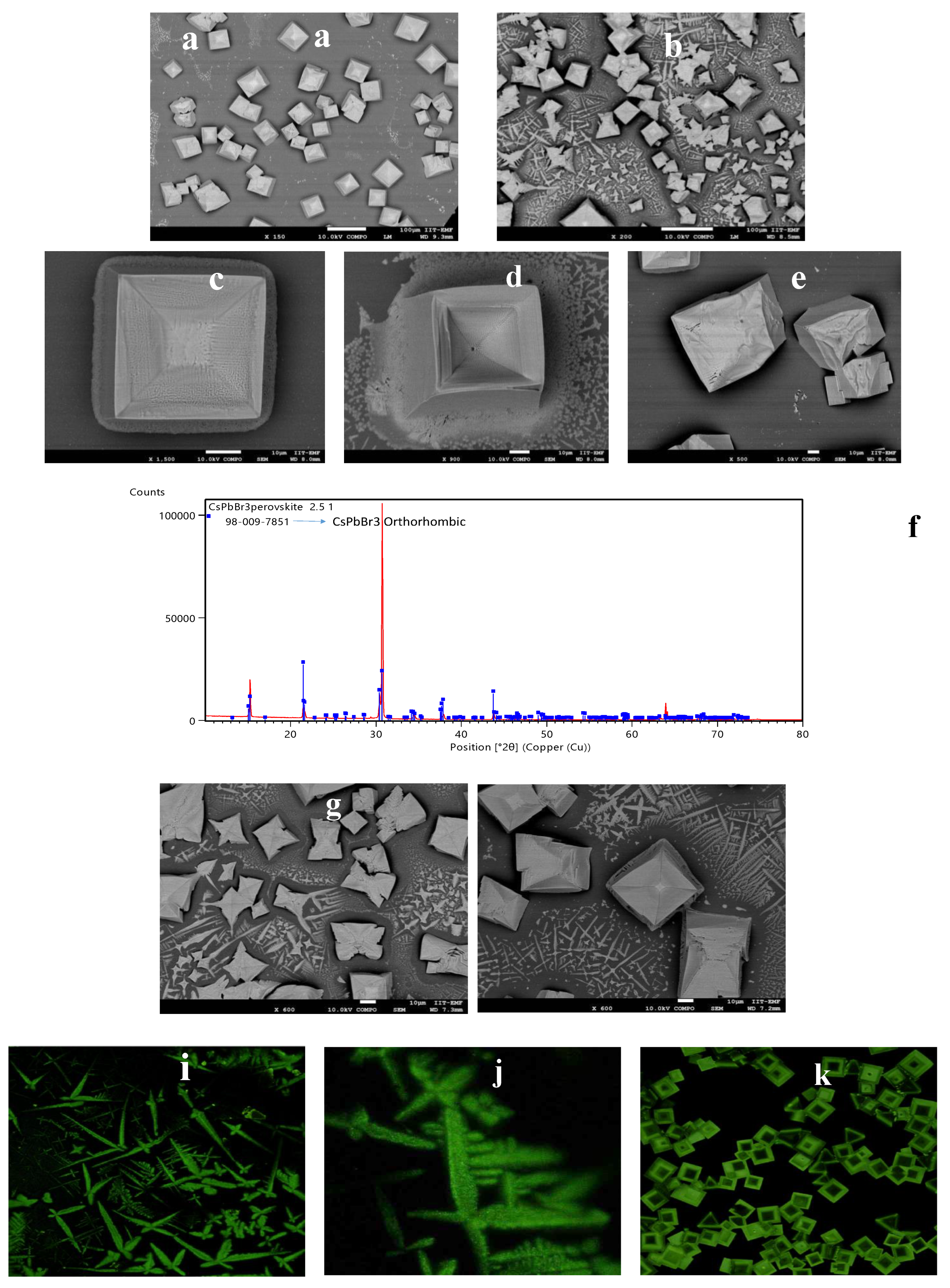
Figure 2.
AFM images of branched CsPbBr3 crystals formed between microcubes (a) top view and (b) corresponding 3D rendering of samples D3 and D4.
Figure 2.
AFM images of branched CsPbBr3 crystals formed between microcubes (a) top view and (b) corresponding 3D rendering of samples D3 and D4.
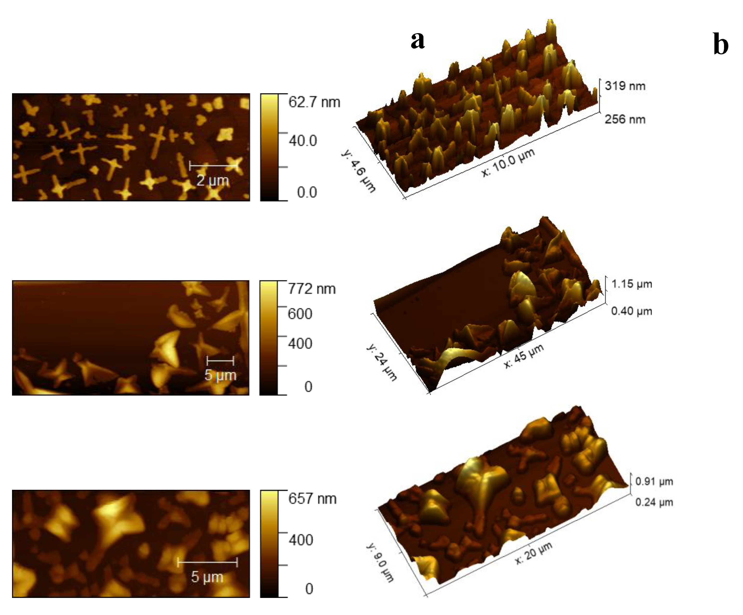
Figure 3.
a,b) Optical micrographs with different magnifications (a) scale bar 300 µm, b) scale bar 50 µm), and c) PL map of sample D1. d,e) Optical micrographs with different magnifications (d) scale bar 40 µm, c) scale bar 10 µm), and PL map of sample D2. g,h) Optical micrographs with different magnifications (g) scale bar 50 µm, h) scale bar 20 µm), and i) PL map of sample D3.
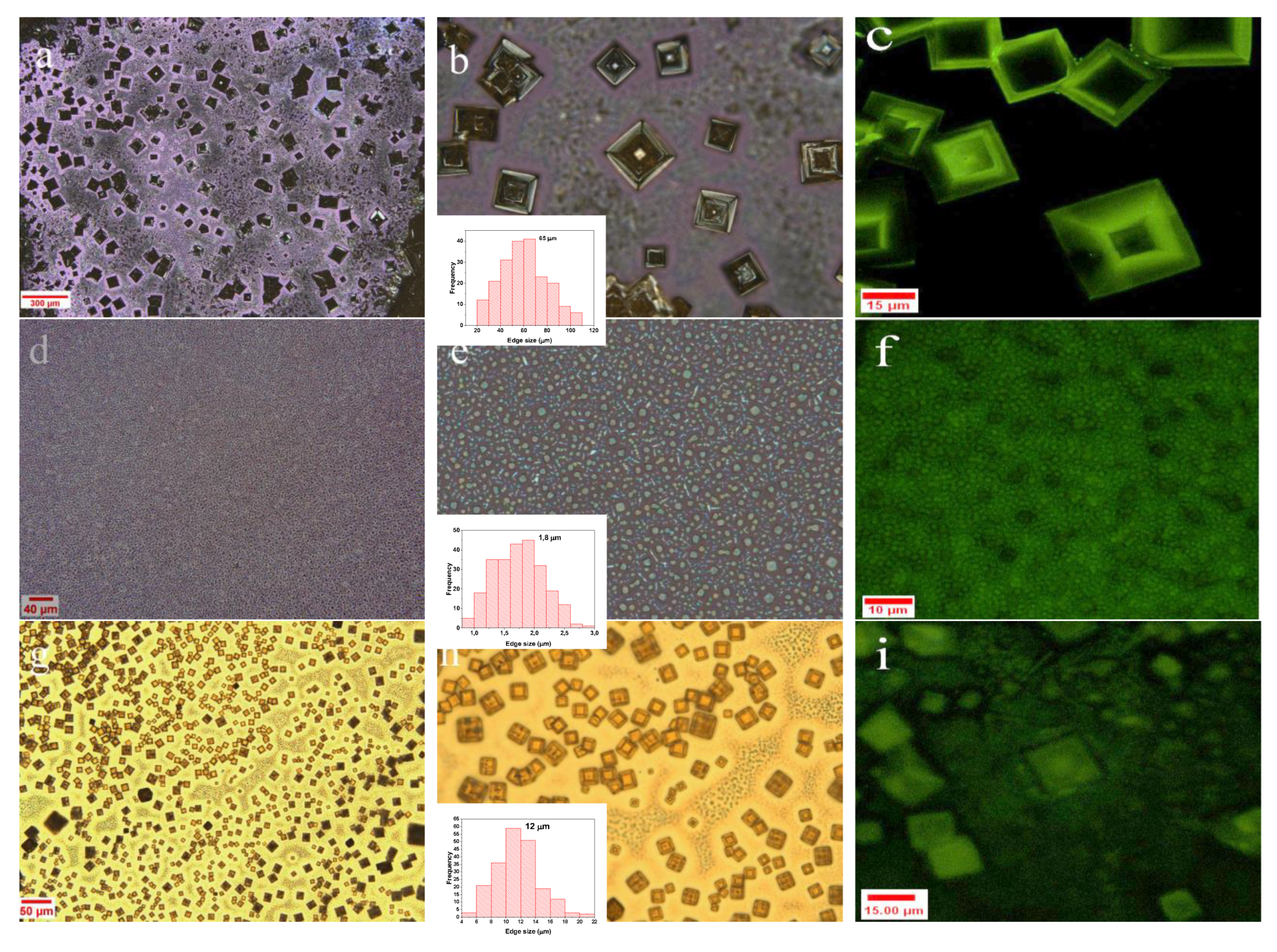
Figure 4.
a,b) Optical micrographs with different magnifications (a) scale bar 50 µm and b) scale bar 20 µm) for sample D3, and c,d) optical micrographs with different magnifications (c) scale bar 50 µm and d) scale bar 20µm) for sample D4. And e,f) optical micrographs with different magnifications (e) scale bar 50 µm and f) scale bar 10µm) for sample D5.
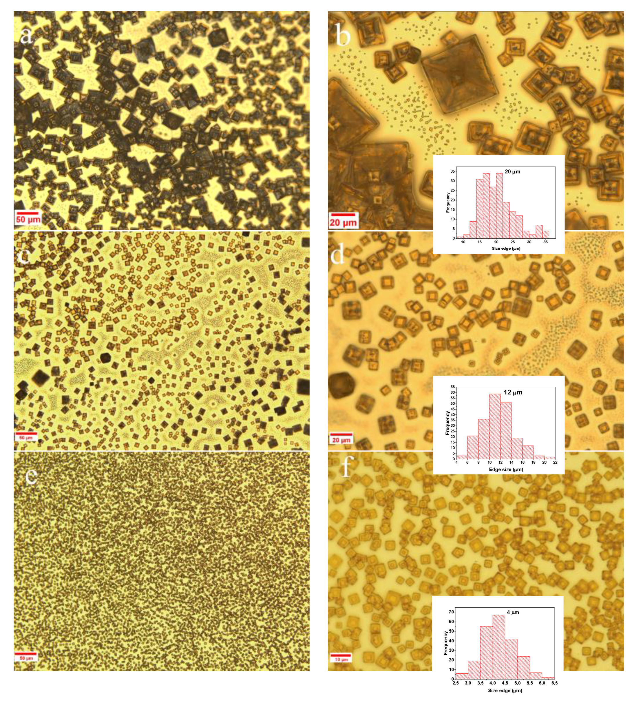
Figure 5.
Microscopic images of sample series D1, D4 and D6) illustrating the change in crystal size as function of annealing temperature (a) 80°C, (b) 120°C and (c) 150°C).
Figure 5.
Microscopic images of sample series D1, D4 and D6) illustrating the change in crystal size as function of annealing temperature (a) 80°C, (b) 120°C and (c) 150°C).
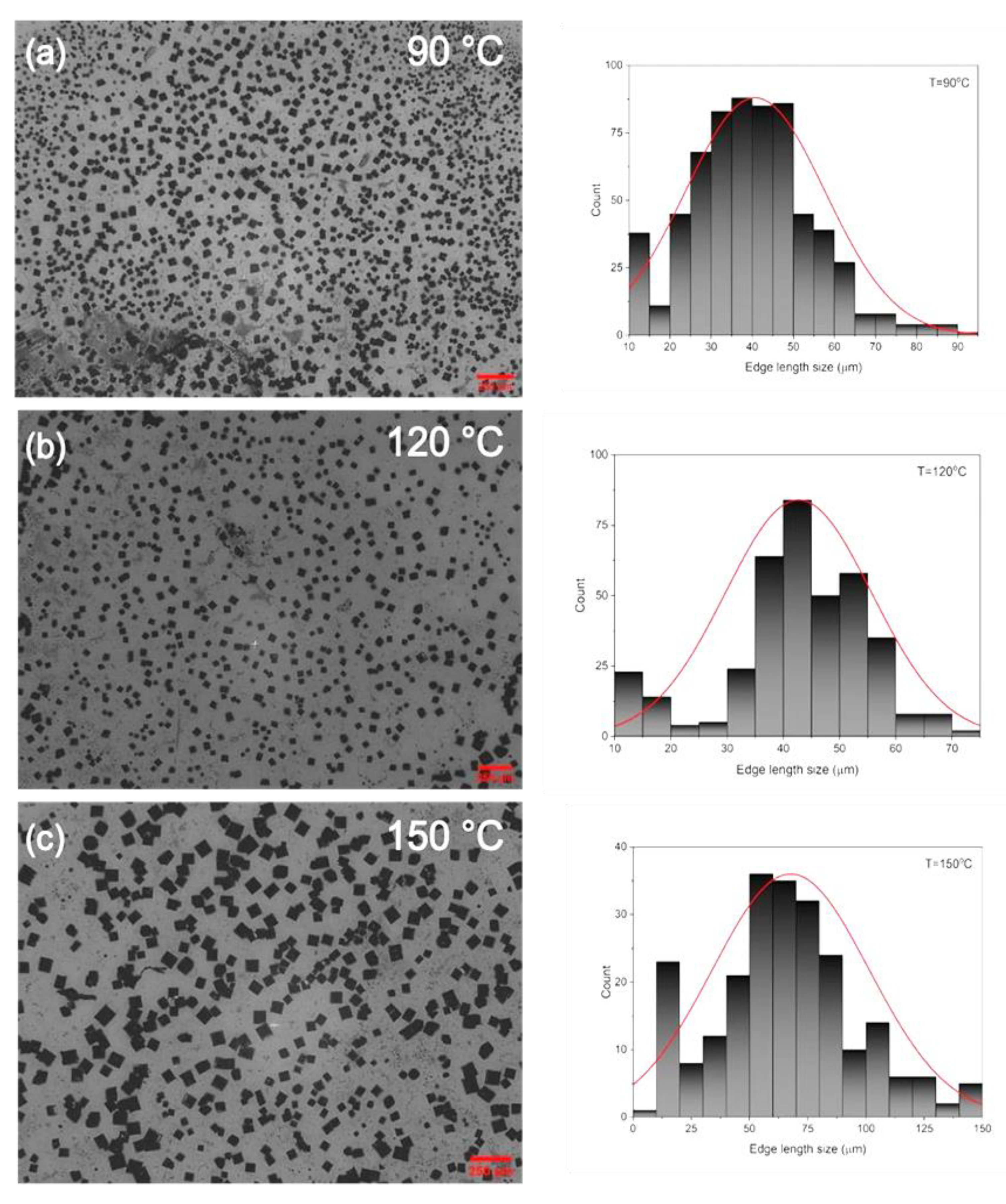
Figure 6.
(a-b) Microscopic images recorded from sample D1 with different magnification (scale bar 28 µm and 15 µm, respectively) and (c) 3D rendering of the latter image (b) with single microcubes. (d-e) Microscopic images recorded from sample D8 with different magnification (scale bar 28 µm and 15 µm, respectively) and (f) 3D rendering of the latter image (e) with single microcubes. (g) schematic illustration of growth process of our samples.
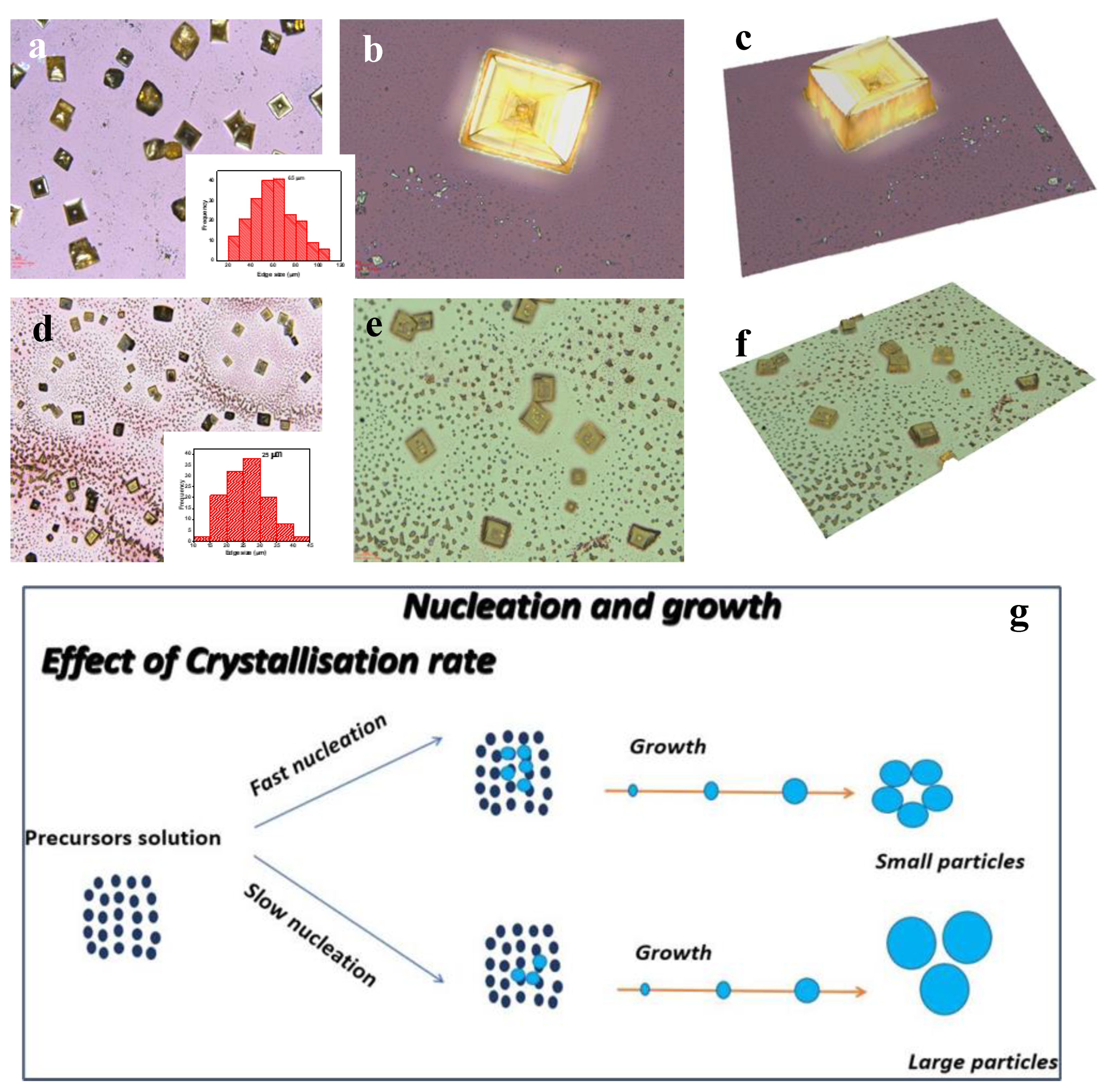
Figure 7.
(a) Schematic representation of solvated species in both precursor solutions with different solvent. (b) Optical measurements of absorbance and PL spectra of the two solutions and (c) DLS measurements on two solvents.
Figure 7.
(a) Schematic representation of solvated species in both precursor solutions with different solvent. (b) Optical measurements of absorbance and PL spectra of the two solutions and (c) DLS measurements on two solvents.
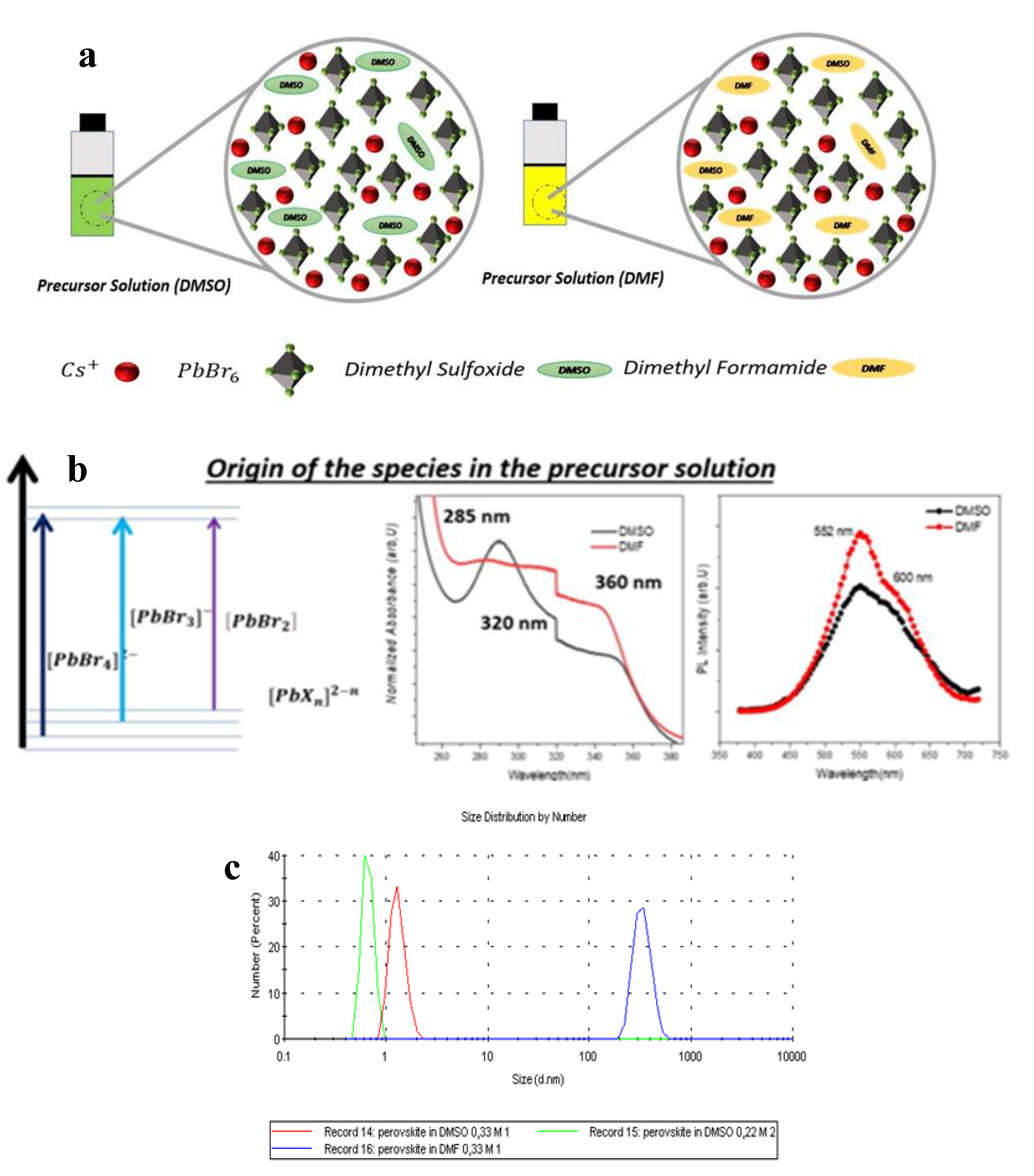
Figure 8.
Optical micrographs of the microcrystals after two months of deposition with two different magnifications (a, b) scale bar 150 µm and c,d) and e) scale bar 28µm.
Figure 8.
Optical micrographs of the microcrystals after two months of deposition with two different magnifications (a, b) scale bar 150 µm and c,d) and e) scale bar 28µm.
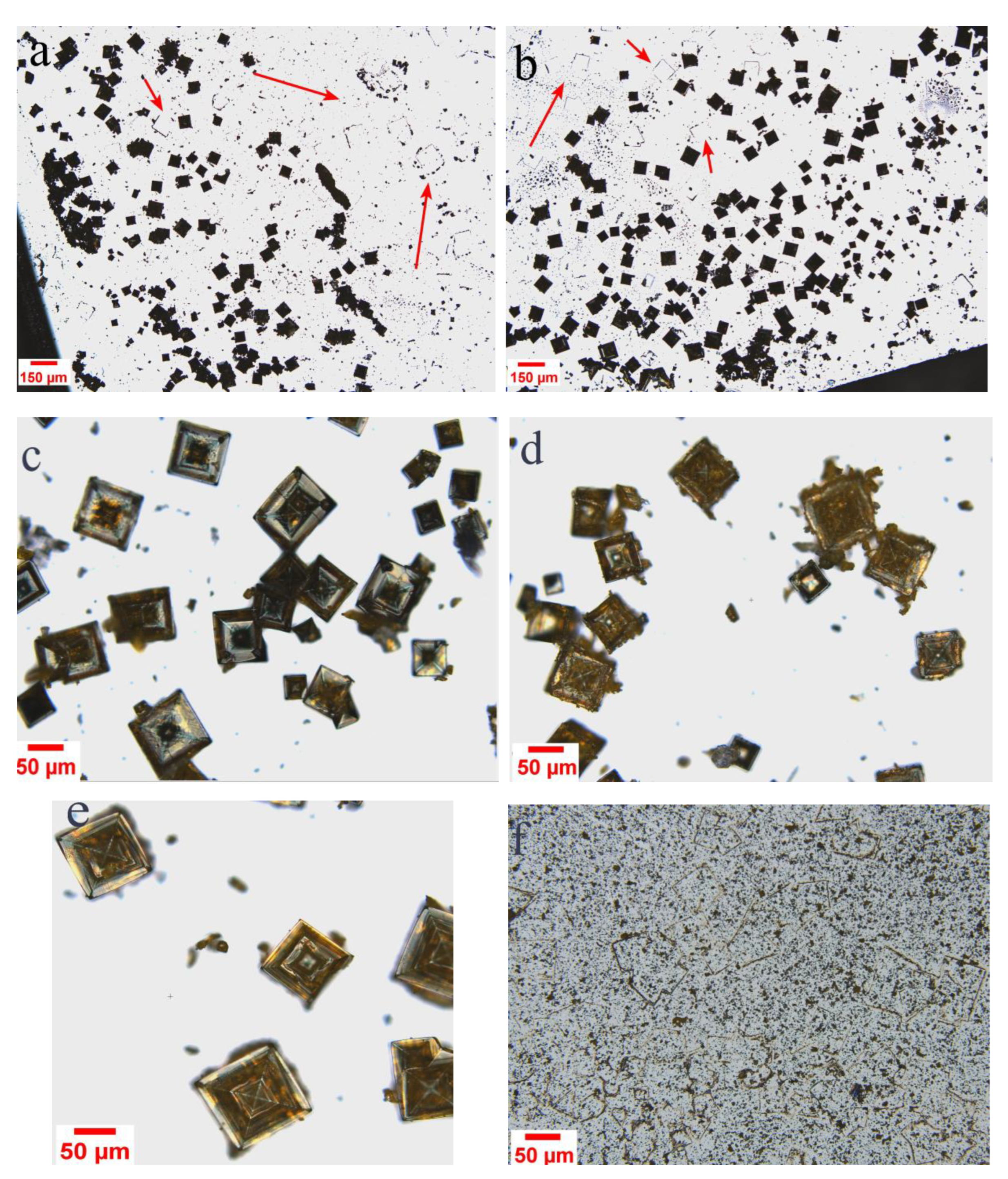
Figure 9.
(a) Micro-PL spectra sequentially acquired on a CsPbBr3 microcrystal at 300 K for different illumination times (λ=350nm). (b-d) Optical micrographs of single microcrystal before and after illumination.
Figure 9.
(a) Micro-PL spectra sequentially acquired on a CsPbBr3 microcrystal at 300 K for different illumination times (λ=350nm). (b-d) Optical micrographs of single microcrystal before and after illumination.
Disclaimer/Publisher’s Note: The statements, opinions and data contained in all publications are solely those of the individual author(s) and contributor(s) and not of MDPI and/or the editor(s). MDPI and/or the editor(s) disclaim responsibility for any injury to people or property resulting from any ideas, methods, instructions or products referred to in the content. |
© 2026 by the authors. Licensee MDPI, Basel, Switzerland. This article is an open access article distributed under the terms and conditions of the Creative Commons Attribution (CC BY) license (http://creativecommons.org/licenses/by/4.0/).
Copyright: This open access article is published under a Creative Commons CC BY 4.0 license, which permit the free download, distribution, and reuse, provided that the author and preprint are cited in any reuse.


