Submitted:
02 January 2026
Posted:
04 January 2026
You are already at the latest version
Abstract
Chiplet technology enables the integration of heterogeneous dies into a single system, of-fering improved performance, scalability, and design flexibility. To support chiplet-based architectures, advanced packaging methods such as System-in-Package (SiP), 2.5D inter-posers, and 3D stacking are essential. A key enabler in these technologies is the fine-pitch Redistribution Layer (RDL), which ensures high interconnect density, signal integrity, and thermal efficiency. This study presents the development and optimization of fine-pitch RDL for two inter-poser types—2.5D RDL interposers and Embedded Bridge Die interposers—fabricated using fan-out wafer-level packaging (FOWLP). A newly developed positive photoresist was used in the photolithography process to define sub-micron RDL features. Process pa-rameters such as exposure energy and focus settings were systematically optimized to improve pattern resolution and structural integrity. Experimental results demonstrated that optimized lithographic conditions significantly enhanced the fidelity and uniformity of fine-pitch RDLs, enabling reliable signal trans-mission and manufacturability in multi-die systems. The findings confirm that fine-pitch RDL is a foundational technology for next-generation interposer solutions, supporting tighter die spacing and improved system performance. This technology can be imple-mented across various chiplet-based packaging platforms, such as those used in next generation artificial intelligence (AI) processors and high-performance computing (HPC) architectures.
Keywords:
FOWLP (FanOut Wafer Level Package)
; interposer
; chiplet
; advanced packaging
; fine pitch RDL
1. Introduction
The continued drive for higher integration, bandwidth, and energy efficiency has positioned advanced packaging as a key enabler of system-level performance. Among various approaches, Fan-Out Wafer-Level Packaging (FOWLP) has gained prominence by eliminating traditional substrates and forming redistribution layers (RDLs) on mold or polymer dielectrics, thereby providing high I/O density, shortened interconnects, and compact form factors [1–3]. This direction aligns with the broader transition toward heterogeneous integration and chiplet-based architectures, where manufacturable, fine-pitch interconnects with low parasitics are required for AI and high-performance computing (HPC) applications [1,4].
Despite this progress, reliably realizing fine-pitch RDLs at and below the 5 μm regime over non-planar topographies and relatively thick dielectric stacks typical of FOWLP and panel-level processes remains challenging. Die to die interconnections in 2.5D interposers require patterns of below than 2/2um line and space [5]. Conventional lithography flows are constrained by depth-of-focus limitations, topography-induced image distortion, and variability in thick photoresist processing, which can limit pattern fidelity, yield, and scalability [2,6]. To mitigate these issues, multiple complementary strategies have been investigated. These include material innovations such as chemically amplified positive photoresists (CAR) and tailored underlayers to manage acid generation and diffusion and to reduce line-edge roughness (LER) [6,7]; optical and process advances including high-NA stepper imaging, improved focus/leveling and topography compensation, and enhanced inspection/metrology to tighten CD control across die and panel formats [3,8]; adoption of dry-film polymer dielectrics and panel-scale lithography to improve coating uniformity and enable high-aspect-ratio trench RDLs on large substrates [3,10]; and interconnect architecture optimization using fine-pitch multi-metal RDL stacks co-optimized for chiplet accelerators and 2.5D/3D integration [1,4]. These efforts have demonstrated the feasibility of 2 μm-class line/space (L/S) features and, in some panel processes, sub-micrometer trench structures [1,3,8]. Nevertheless, consistent pattern fidelity, adequate process latitude, and material compatibility across sub-5 μm RDLs require further improvement for high-volume manufacturing [2,5,8].
In this work, we focus on FOWLP-oriented implementation of fine-pitch RDLs for advanced packaging. We introduce a chemically amplified positive photoresist and systematically optimize key photolithography parameters—exposure energy, focus offset, and soft-bake conditions—to establish a manufacturable process window for reliable 2 μm/2 μm L/S fabrication. The approach emphasizes improved LER, sidewall quality, and post-plating structural robustness while minimizing dependence on overly complex multilayer stacks or specialized tooling. The results are intended to support the practical deployment of fine-pitch RDLs in FOWLP for advanced packages, with attention to scalability and compatibility with downstream processes [1,4,8].
2. Materials and Methods
To ensure high pattern fidelity essential for stable electrical performance and yield in semiconductor devices, this study aims to establish optimized photolithography parameters through systematic experimentation and analysis. By evaluating the influence of various lithographic conditions, we provide valuable insights into scalable manufacturing for next-generation semiconductor packaging.
For fine pattern formation, a chemically amplified resist (CAR) was selected due to its superior performance in micro-lithography. CAR resists generate acid upon UV exposure via a photo acid generator (PAG), which then catalyzes chemical reactions within the resist matrix during the PEB step. This process increases the solubility of the exposed regions, enabling selective removal during development. CAR resists consist of a polymer, PAG, and solvent. The acid generated during exposure does not degrade but acts catalytically, interacting with multiple polymer chains, hence the term "chemically amplified." This mechanism allows CAR to achieve high contrast even with short exposure times [6].
The chemical amplification characteristics of CAR enable extremely high resolution. In particular, reducing line edge roughness (LER) is directly linked to device performance. Recent studies have shown that suppressing acid diffusion and optimizing post-development treatments can significantly reduce LER, which is critical for maintaining signal integrity in advanced packaging [6,7]. Furthermore, the reaction front propagation model suggests that acid diffusion during post-exposure bake (PEB) is enhanced by transient free volume generation and plasticization, which accelerates deprotection but may also lead to pattern distortion if uncontrolled [6]. Lithographic performance is highly sensitive to PEB temperature relative to the polymer’s glass transition temperature (Tg); optimal resolution is achieved near Tg, while excessive temperatures can cause resist hardening and linewidth narrowing [6].
2.1. Photoresist Material and Thickness Control
Photoresist (PR) materials are essential for defining fine patterns with high precision in semiconductor and advanced packaging processes. The PXi-series CAR, provided by a Japanese manufacturer, exhibits robust line/space patterning capability and is optimized for applications requiring fine pattern fidelity and film-thickness uniformity.
Accurate control of PR thickness is critical because it directly affects subsequent electroplating step heights and interconnect geometry. In parallel, minimizing resist roughness—both at the surface and at line edges—is essential to preserve pattern fidelity in fine-pitch RDLs. Recent work has demonstrated process schemes to reduce roughness in chemically amplified resists (CAR), indicating that appropriate material/process tuning can improve imaging quality and dimensional stability for next-generation lithography [10].

Table 1.
This is a table. Tables should be placed in the main text near to the first time they are cited.
Table 1.
This is a table. Tables should be placed in the main text near to the first time they are cited.
| Viscosity | DOF | Design Film Thickness | Resolution |
|---|---|---|---|
| 80cp | 25um | 3~12um | L/S 2/2um Capability |
Accurate control of PR thickness is crucial in semiconductor and advanced packaging processes, as it directly affects the thickness of subsequent electroplating layers. Variations in PR thickness can significantly impact the final product’s quality and electrical performance. Therefore, precise control of PR thickness is essential to ensure optimal outcomes in electroplating processes.
In this study, spin coating was employed to control the PR thickness. The objective was to investigate the influence of spin coating parameters—such as spin speed, solution viscosity, spin time, and dispense volume—on the resulting PR film thickness. The PR thickness was measured using an optical profiler, with measurements taken at nine different points on each sample to evaluate coating uniformity.
Spin coating is a widely adopted technique for depositing uniform thin films onto flat substrates. In this process, a small amount of liquid photoresist is dispensed at the center of the substrate, which is then rotated at a speed optimized for the material properties of the solution. The centrifugal force distributes the material evenly across the surface, forming a thin film. The final film thickness is primarily influenced by the spin speed, solution viscosity, and spin duration. By precisely adjusting the spin speed according to the rheological characteristics of the photoresist, the film thickness can be accurately controlled to meet specific application requirements. Figure 1 illustrates the experimental results of controlling photoresist thickness to a target value of 5 μm using spin speeds ranging from 700 to 1000 rpm. Among the tested conditions, 800 rpm was found to be the most suitable spin speed for achieving the desired film thickness with optimal uniformity.
Figure 2 shows the image of the photoresist thickness measurement obtained using a KLA-Tencor Nanospec system, following exposure and development with a fine pattern mask on a wafer coated at 800 rpm.
2.2. Exposure and Soft Bake Process Conditions
To evaluate the resolution and pattern fidelity of fine-pitch photoresist structures, a series of photolithography experiments were conducted using a broadband exposure system operating in the 300–500 nm wavelength range. The exposure energy was varied from 90 mJ/cm2 to 300 mJ/cm2, and the focus offset was adjusted within a ±5 μm range to assess the impact on critical dimension (CD) control.
In parallel, the soft bake (prebake) process was optimized to ensure uniform solvent evaporation and stable resist film formation prior to exposure. The soft bake temperature was varied between 90 °C and 130 °C, and the bake time was adjusted from 60 to 180 seconds. These parameters were systematically correlated with the exposure conditions to determine their combined effect on resist profile, resolution, and pattern collapse resistance.
The experimental matrix was designed to explore the interdependence between exposure wavelength, energy dose, focus setting, and soft bake conditions. This approach enabled the identification of optimal process windows for achieving high-resolution 2 μm/2 μm line/space patterns using chemically amplified photoresist (CAR) materials.
Figure 3.
(a) Exposure process conducted on a wafer with soft bake conditions set at 90 °C; (b) soft bake conditions set at 120 °C. For both wafers, exposure conditions were categorized from A to H based on different positional parameters across the wafer surface.
Figure 3.
(a) Exposure process conducted on a wafer with soft bake conditions set at 90 °C; (b) soft bake conditions set at 120 °C. For both wafers, exposure conditions were categorized from A to H based on different positional parameters across the wafer surface.
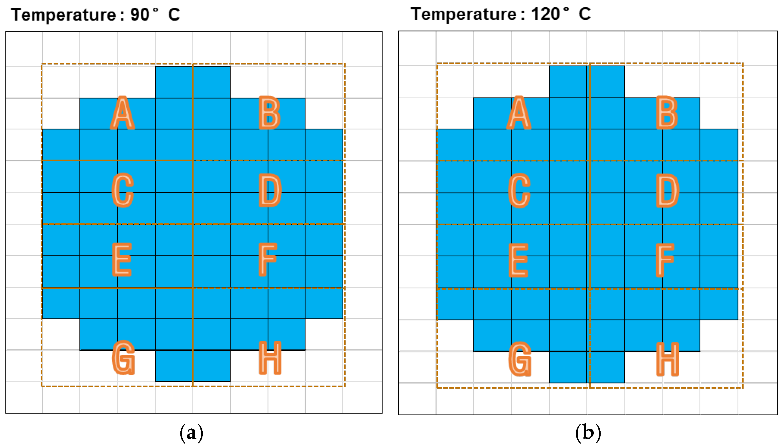
Based on the experimental results obtained under the aforementioned conditions, the most suitable process parameters were identified through image based analysis. The optimal conditions were clearly distinguished and annotated for each parameter set.
Figure 4 shows the image obtained from measurements of photoresist thickness and fine-pattern regions after exposure and development. The wafer was coated with photoresist at 800 rpm and exposed using a fine-pattern mask with 2 μm/2 μm line/space features. The exposure energy and development conditions were optimized for the given process, and the measurements were performed using a KLA-Tencor Nanospec system.
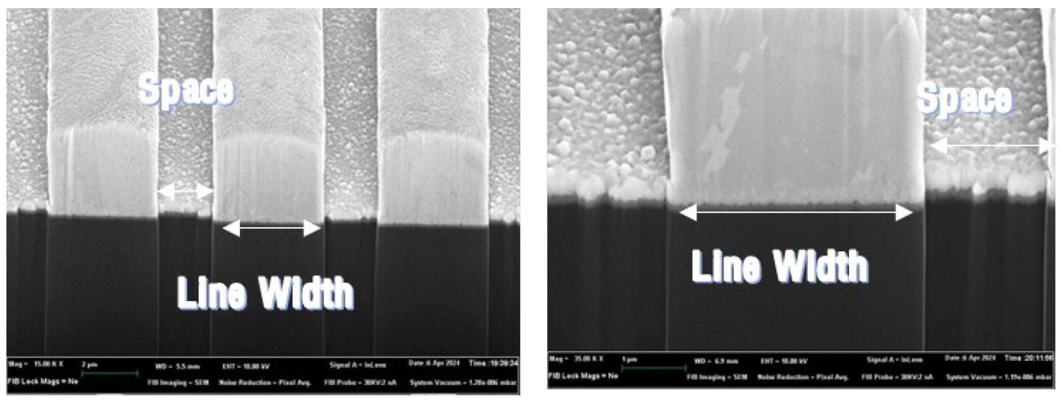
Figure 5 presents the cross-sectional analysis performed to verify the final structure of the redistribution layer (RDL) after completing the photolithography and electroplating processes, followed by the photoresist stripping step and prior to seed layer etching. To clearly observe the formation of the 2 μm/2 μm line/space structure, a Focused Ion Beam (FIB) image was acquired. As shown in Figure 5, the analysis confirms that both the line width and space were successfully and accurately formed, demonstrating high pattern fidelity and structural precision.
Figure 6.
FIB cross-sectional image of the L/S 2 μm/2 μm region, obtained after photoresist patterning, electroplating, and completion of the PR strip process. The image provides detailed structural analysis of the fine-pitch features at the final stage of fabrication.
Figure 6.
FIB cross-sectional image of the L/S 2 μm/2 μm region, obtained after photoresist patterning, electroplating, and completion of the PR strip process. The image provides detailed structural analysis of the fine-pitch features at the final stage of fabrication.
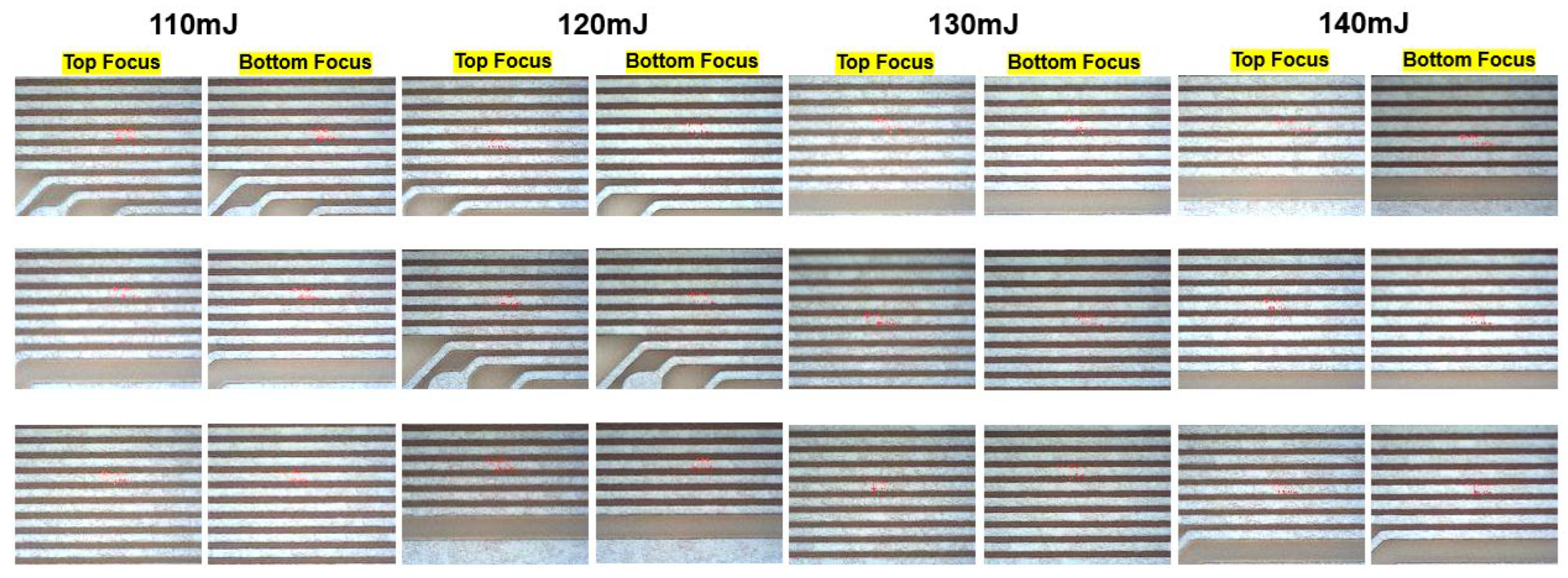
The images below were obtained after completing the electroplating and etching processes using patterns formed under various exposure conditions. The results confirm that exposure conditions had no significant impact on the final pattern formation, as no observable differences were detected in the structural integrity or geometry of the plated features.
Figure 7.
This is a figure. Schemes follow the same formatting.
3. Results
This study introduces a novel photolithography process utilizing a newly developed positive photoresist, overcoming limitations of conventional RDL fabrication methods in achieving sub-micron resolution and multi-layer uniformity. Through optimization of exposure energy and focus settings, fine-pitch RDLs with enhanced pattern fidelity and structural integrity were successfully realized [1,8].
A comprehensive analysis was conducted on the effects of various lithographic parameters—including exposure energy, focus offset, soft bake temperature, and bake time—on the formation of fine patterns. The results demonstrated that these parameters significantly influence the structural integrity and dimensional accuracy of the line and space (L/S) features. Notably, soft bake and post-exposure bake (PEB) conditions were found to play distinct roles in resist performance: soft bake ensures solvent removal and film uniformity, while PEB governs acid diffusion and resolution enhancement [6].
At lower exposure energies, the PR patterns failed to develop properly, resulting in pattern collapse and deformation, consistent with capillary-force-induced collapse models and the reduced mechanical robustness of insufficiently cross-linked features [6,12]. Conversely, excessive soft bake temperatures led to narrowing of the PR features, indicating over-hardening of the resist film due to accelerated crosslinking and reduced acid mobility [6].
Through systematic optimization, the most suitable process window was identified, enabling the formation of uniform 2 μm/2 μm L/S patterns with high fidelity. The optimized PR thickness and pattern geometry were validated through FIB (Focused Ion Beam) analysis after electroplating and prior to seed etching, confirming the structural integrity of the fabricated RDL.
By integrating the optimized PR material and process conditions, fine-pitch RDLs were successfully fabricated and electroplated, demonstrating the practical applicability of the proposed approach in advanced packaging. This confirms the viability of the developed process for next-generation semiconductor interconnect technologies. Additionally, improvements in resist roughness were associated with enhanced dimensional stability of 2 μm/2 μm features, in agreement with recent CAR roughness-reduction studies [10].
4. Discussion
The experimental results presented in this study demonstrate the effectiveness of the proposed photolithography process in achieving high-resolution fine-pitch RDL structures using a chemically amplified positive photoresist. Compared to conventional RDL fabrication methods, which often struggle with sub-micron resolution and pattern uniformity, the optimized process parameters—particularly exposure energy, focus settings, and soft bake conditions—enabled the formation of stable 2 μm/2 μm line/space patterns with high fidelity. In line with prior studies on roughness mitigation in chemically amplified resists, reducing resist roughness contributed to improved line-edge quality and overall pattern fidelity in the 2 μm/2 μm L/S regime [10].
The use of a chemically amplified resist (CAR) proved to be a critical factor in enhancing resolution, which is essential for maintaining signal integrity and electrical performance in advanced semiconductor devices [5,6]. The systematic variation and analysis of lithographic conditions revealed that insufficient exposure energy leads to pattern collapse, while excessive thermal treatment causes resist hardening and feature narrowing. These findings underscore the importance of precise control over both optical and thermal process variables.
Furthermore, the successful integration of the optimized photoresist and process conditions into a fan-out wafer-level packaging (FOWLP) framework validates the scalability and manufacturability of the proposed approach. The ability to fabricate fine-pitch RDLs with consistent structural integrity across multiple layers supports the development of next-generation interposer technologies for chiplet-based systems, where high interconnect density and low parasitics are critical.
Future work will focus on extending the process compatibility to various design geometries and evaluating long-term reliability under thermal and mechanical stress conditions.
5. Conclusions
This study successfully demonstrates the feasibility of implementing fine-pitch RDL (Redistribution Layer) interposer technology based on Fan-Out Wafer-Level Packaging (FOWLP) by optimizing the photolithography process using a newly developed chemically amplified positive-type photoresist. The primary objective was to achieve a stable 2 μm/2 μm line/space configuration, which is critical for enabling high-density interconnects in 2.5D and chiplet integration technologies.
Through systematic experimentation, we investigated the effects of key lithographic parameters—including exposure energy, focus settings, and post-exposure bake (PEB) conditions such as temperature and duration—on the resolution and integrity of the patterned features. The results revealed that insufficient exposure energy led to pattern collapse, while excessive bake temperatures caused narrowing of the PR features. These findings underscore the importance of finely tuned process conditions in achieving high-fidelity pattern transfer.
The use of a chemically amplified resist (CAR) enabled superior resolution, which are essential for maintaining the electrical performance and reliability of advanced semiconductor devices. The optimized process conditions established in this study significantly improved the pattern fidelity and structural integrity of the RDL, thereby validating the potential of FOWLP-based RDL interposer technology for next-generation high-density electronic packaging.
This work provides valuable insights into the scalable manufacturing of fine-pitch RDLs and highlights the critical role of advanced photoresist materials and precise process control in the evolution of semiconductor packaging technologies.
Building upon the material characteristics validated in this study, future research will focus on the implementation of multi-layer RDL structures. This includes the design and fabrication of complex interposer architectures tailored to support high-density chiplet integration. Each additional layer will be accompanied by a thorough evaluation of structural integrity, electrical performance, and process compatibility, ensuring that the proposed methodology remains scalable and robust across diverse packaging configurations.
References
- Lau, J.H., Ed. Fan-Out Wafer-Level Packaging; Springer: Singapore, 2018; 269–303. [CrossRef]
- Ashraf, N.S., Ed. Handbook of Emerging Materials for Semiconductor Industry; Springer: Singapore, 2024; 241–252. [CrossRef]
- Khalkhal, F.; Chaney, K.H.; Muller, S.J. Optimization and Application of Dry Film Photoresist for Rapid Fabrication of High-Aspect-Ratio Microfluidic Devices. Microfluid. Nanofluid. 2016, 20, 153. [CrossRef]
- Lau, J.H. Chiplet Design and Heterogeneous Integration Packaging; Springer: Singapore, 2023; 1–99. [CrossRef]
- J.Kim., Fan-Out Panel Level Package with Fine Pitch Pattern, Electronic Components and Technology Conference(ECTC) 2018, May 2018.
- Bulgakova, S.A.; Kiryukhin, D.P.; Tsvetkov, N.P.; Rukin, S.N.; Eto, M.; Afanas’ev, V.P. Chemically Amplified Resists for High-Resolution Lithography. Russ. Microelectron. 2013, 42, 206–217. [CrossRef]
- Bickel, S.; Stöhr, R.; Kostecki, R.; Poppe, A.; Böttger, U.; Engelmann, S.; Schroth, A.; Ostmann, A.; Lang, K.-D. Fine-Pitch Copper Nanowire Interconnects for 2.5/3D System Integration. J. Electron. Mater. 2024, 53, 4410–4420. [CrossRef]
- Ashraf, N.S. Advanced Lithographic Techniques for Sub-nm Lithographic Resolution of Feature Length. In Handbook of Emerging Materials for Semiconductor Industry; Ashraf, N.S., Ed.; Springer: Singapore, 2024; 241–252. [CrossRef]
- Choi, M.; Porter, S.C.; Meisen, A. Interrelationships Between Coating Uniformity and Efficiency in Pan Coating Processes. AAPS PharmSciTech 2021, 22, 265. [CrossRef]
- Cho, K.; Dinh, C.Q.; Tomori, H.; Nagahara, S.; Hara, A.; Fujimoto, S.; Muramatsu, M. A Novel Process to Reduce Roughness in Chemically Amplified Resist (CAR) for Next-Generation Lithography. Photopolym. Sci. Technol. 2024, 37, 251–256. [CrossRef]
- Namatsu, H.; Yamaguchi, T.; Yamazaki, K.; Yamagata, Y.; Kurihara, K. Supercritical Drying for High-Aspect-Ratio Resist Nanostructures. J. Vac. Sci. Technol. B 1998, 16, 69–76. [CrossRef]
- Tanaka, T.; Morigami, M.; Atoda, N. Mechanism of Resist Pattern Collapse during Rinse Process. J. Vac. Sci. Technol. B 1993, 11, 2748–2752. [CrossRef]
Figure 1.
The spin coating process as influenced by the viscosity of the photoresist material.
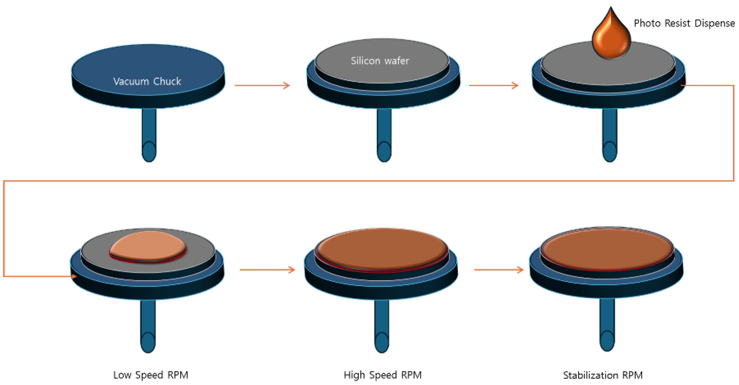
Figure 2.
Coating Thickness Variation by Spin RPM.
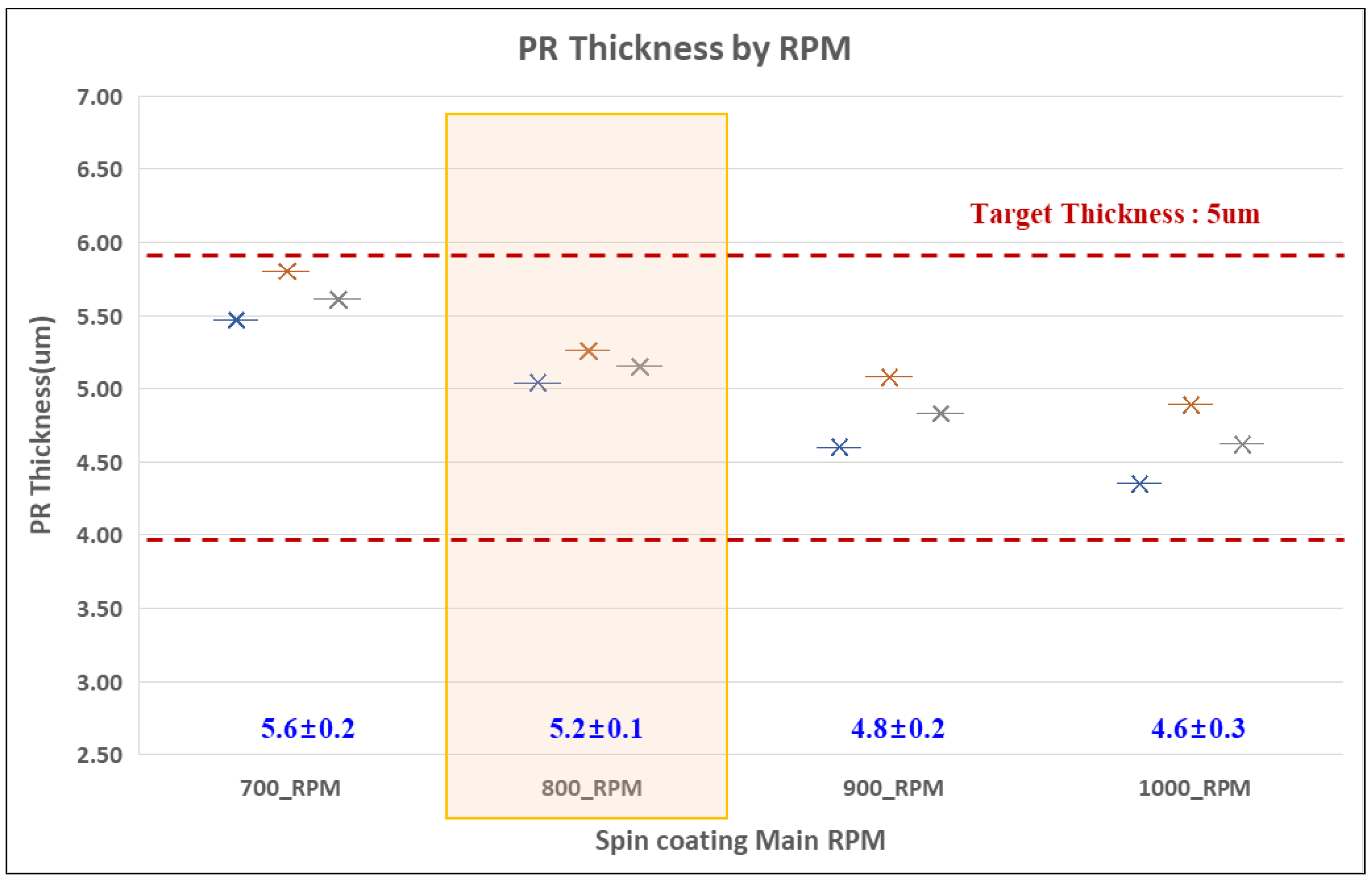
Figure 4.
(a) Exposure process conducted on a wafer with soft bake conditions set at 90 °C; (b) Exposure process conducted on a wafer with soft bake conditions set at 120 °C. For both wafers, exposure conditions were categorized from A to H based on different positional parameters across the wafer surface.
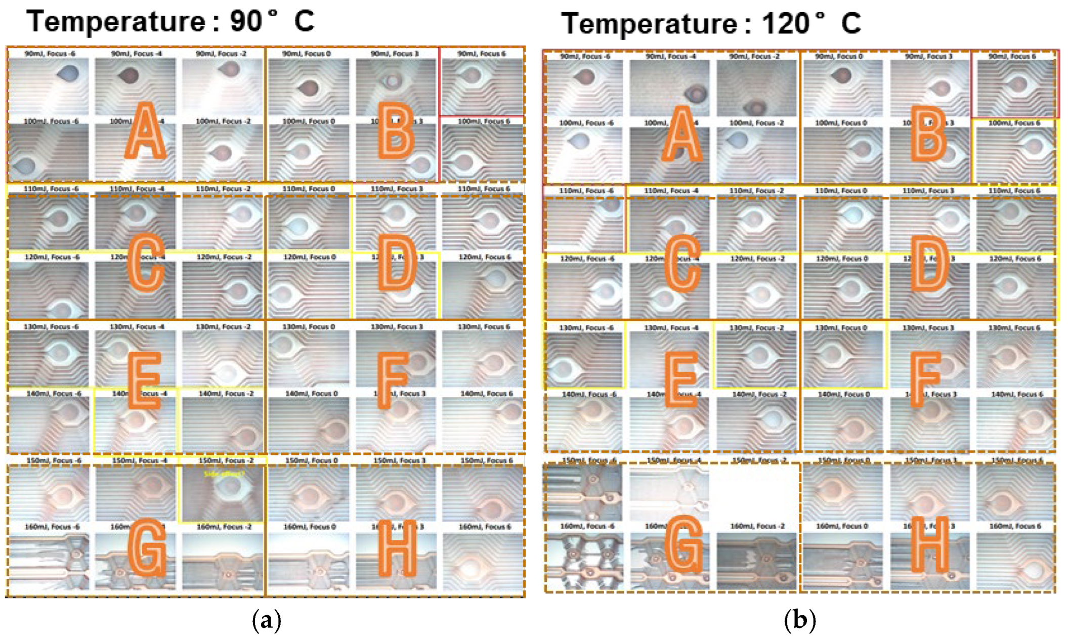
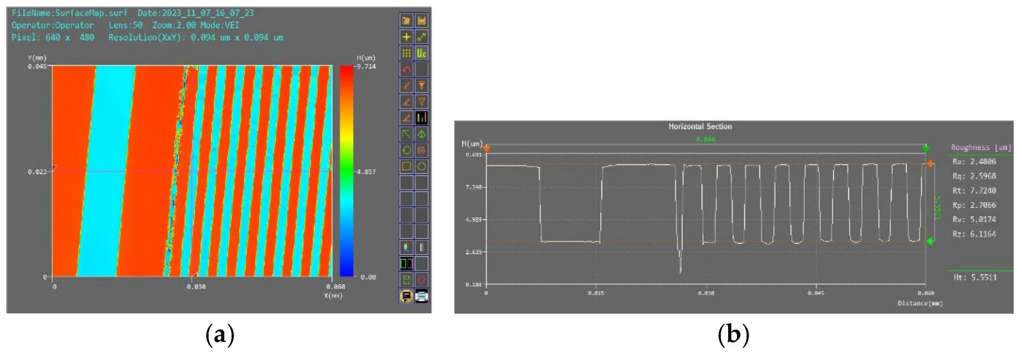
Figure 5.
(a) displays the screen image of the completed 2 μm/2 μm line/space fine pattern region after the photolithography process. (b) presents the corresponding screen image showing the measured photoresist thickness profile across the patterned area.
Figure 5.
(a) displays the screen image of the completed 2 μm/2 μm line/space fine pattern region after the photolithography process. (b) presents the corresponding screen image showing the measured photoresist thickness profile across the patterned area.
Disclaimer/Publisher’s Note: The statements, opinions and data contained in all publications are solely those of the individual author(s) and contributor(s) and not of MDPI and/or the editor(s). MDPI and/or the editor(s) disclaim responsibility for any injury to people or property resulting from any ideas, methods, instructions or products referred to in the content. |
© 2026 by the authors. Licensee MDPI, Basel, Switzerland. This article is an open access article distributed under the terms and conditions of the Creative Commons Attribution (CC BY) license (http://creativecommons.org/licenses/by/4.0/).
Copyright: This open access article is published under a Creative Commons CC BY 4.0 license, which permit the free download, distribution, and reuse, provided that the author and preprint are cited in any reuse.


