
Submitted:
25 November 2024
Posted:
26 November 2024
You are already at the latest version
Abstract
In this research, 3D Mechatronic Integrated Devices (3D-MID) components are fabricated using Stereolithography (SLA) 3D printing and laser direct structuring (LDS) technologies. A process flow for 3D-MID fabrication based on SLA technology is developed to explore the miniaturization potential of these components. The results demonstrates that electric circuits can be successfully formed on substrates printed with resin mixed with LDS additives, following the laser structuring and metallization processes. The introduction of vias and the use of different packaging types enables the circuit to be miniaturized, with a minimum distance of 150 µm between conductive tracks, and the usage of BGA surface-mounted devices. The 3D-MID components based on SLA 3D printing technology exhibit significant potential for miniaturization, not only facilitating the integration of complex circuits and high-precision wiring but also offering broad support for the development of miniaturized electronic devices and systems.
Keywords:
mechatronic integrated devices
; laser direct structuring
; SLA
; miniaturization
1. Introduction
3D Mechatronic Integrated Devices (3D-MID) can effectively integrate mechanical, thermal, optical, and electrical functions due to their geometric design flexibility and the combination of selective structuring and metallization. This renders them widely utilized in various applications, such as automotive, medical technology, IT and telecommunications, and industrial automation [1]. Due to the unique three-dimensional structure and small batch production characteristics of 3D-MID components, the traditional injection molding process for manufacturing circuit carriers faces challenges such as high costs, limited design flexibility, long production cycles, and difficulty in handling complex geometries, all of which have become bottlenecks in the development of 3D-MID technology [2]. An innovative and rapid method for producing 3D-MID is to use additive manufacturing technology (AM) that requires no molding tools. Additive manufacturing for 3D-MID not only compensates for the high initial cost of injection molds, but also offers greater design flexibility and faster production cycles [3]. Currently, extensive work is primarily focused on 3D-MID based on Fused Deposition Modeling (FDM) and Selective Laser Sintering (SLS) additive manufacturing technologies [2,4,5]. In order to further expand the application fields of 3D-MID, SLA technology, which offers higher precision and better material properties, can be utilized. High-performance resins used in SLA, such as heat-resistant and high-strength resins, can enhance the performance of 3D-MID components, making them more suitable for demanding environments. The use of these resins extends the stability and reliability of 3D-MID components under high temperature or mechanical loads [6,7,8].
In this work, circuit carriers are manufactured by mixing LDS additives with heat-resistant resin and utilizing SLA 3D printing technology. Taking Temperature Measurement Systems as an example, after the LDS process and metallization, the circuit layout on the circuit carrier is successfully achieved. The introduction of vias and the use of smaller packaged components effectively realize circuit miniaturization.
To verify the feasibility of SLA-3D-MID components in practical applications, the relationship between laser structuring parameters and the resistance of circuits and vias is analyzed using the Response Surface Methodology (RSM). For soldering, Vapor Phase Soldering (VPS) and Reflow Soldering are employed to solder the populated SLA-3D-MID components, ultimately producing SLA-3D-MID parts free of cracks.
2. Materials and Methods
2.1. Circuit Carrier Manufacturing
The manufacturing of the circuit carriers, as shown in Figure 1a–d, utilized two different heat-resistant resins, each with LDS additives added as the printing material. The mixing ratios and mixing methods for each resin are provided in Table 1. To ensure that the LDS additives are fully mixed with the resin, the resin mixture is first stirred in a planetary mixer at 2000 rpm for 3 minutes, followed by mixing in an ultrasonic water bath for 10 minutes. For SLA printers, there are two main configurations: top-down and bottom-up [9]. The SLA 3D printer used in this work, the Mars 4 Ultra from ELEGOO, operates with a bottom-up configuration, as shown in Figure 1e.
The first-layer exposure time and the normal layer exposure time for the mixed resin are shown in Table 2. Other parameter settings follow the default parameters of the original resin.
2.2. The Evaluation Criteria for Miniaturization
In this work, the circuit design is shown in Figure 2a,b, with the only difference being the use of the U2 chip in different packages. The circuit is a temperature measurement system consisting of sensors connected to an AD converter, which requires a level shifter U2 and a voltage regulator U3. The dimensions of the circuit carrier are 18 mm × 25 mm. Equation (1) is used to evaluate the miniaturization, where AU represents the area utilization and S represents the area. The area of the circuit carrier cannot be infinitely reduced; it depends on the total area of the electronic components and the total area of the circuit. The closer the AU is to 1, the better the area utilization.
2.3. LDS and Metallization
As one of the representative 3D-MID methods, LDS, based on laser technology, is frequently used to create an electrically conductive metal layer on the surface of the modified thermoplastic polymer [5]. In this work, the resin used as the SLA 3D printing material is a thermosetting plastic. Due to the additive in the resin (Figure 1b), it is possible to activate the surface, which is carried out in Figure 3 using an infrared pulsed laser (1064 nm) with a pulse duration in the nanosecond range [10].
The chemical electroless metallization process (Cupralux INI, Palladium Post Dip, Nickel HP, Gold HP) from Atotech, Germany, is utilized in this work [10]. After laser structuring, the circuit carrier is metallized according to the process outlined in Figure 4.
Prior to the metallization of the 3D-MID components, the surface is pretreated with Enplate LDS Cleaner 300 solution to prevent excessive metallization caused by circuit miniaturization. After laser structuring, the component is cleaned in an isopropanol ultrasonic bath (Figure 4a) for 10 minutes, rinsed with deionized water, and dried using a high-pressure air blower (Figure 4b). The detailed steps of the metallization process are summarized in Table 4.
3. Results and Disscussion
3.1. Post-Processing of SLA 3D-Printed Circuit Carrier
The dimensions of the sensor circuit carrier are shown in Figure 5. After SLA 3D printing, it is first cleaned with isopropanol/soap water, then undergoes UV curing (TR300 for 30 minutes, UW for 10 minutes), and is finally placed in an oven at 200°C for 1 hour.
The experiment includes three control groups, with cleaning liquids for the sensor circuit carrier set as isopropanol, soap water, and a combination of soap water cleaning with simultaneous UV curing (simultaneously). After post-processing, the dimensions of each group are measured, with the results shown in Figure 6.
From the box plot in Figure 6, it can be concluded that the treatment of resin samples with isopropanol (shown in blue in Figure 6) is the most effective, as it shows the least variation and the highest stability. The simultaneous cleaning and curing process shows greater variation due to scattering of the UV light as it enters the liquid, preventing it from accurately reaching the surface of the part to be cured.
3.2. The Miniaturization of Circuits
The miniaturization of circuits includes the following three aspects: the introduction of vias, the reduction of spacing between traces and chips with smaller packaging specifications.
3.2.1. Via Holes
Via refers to the vertical electrical connection between two conductor layers [12]. Structures as shown in Figure 7 are created on both the front and back sides of the printed circuit carrier using laser drilling with the LPKF Fusion3D 1100.
A specific limitation in 3D-MID design is that the layer structure can only support a maximum of two layers and lacks a ground plane, requiring all grounding to be connected through routing [13]. Therefore, vias are even more essential to route connections on both sides of the 3D-MID structure. The circuit is arranged on the front side of the circuit carriers in Figure 8a and the back side in Figure 8b, with connections established through vias.
The laser parameters for via holes are investigated using Response Surface Methodology (RSM) and screening experimental design. The RSM method uses a Box-Behnken design. The factors and levels are shown in Table 5. The 29 experiments for each of the two resins are shown on the substrate in Figure 9.
Figure 9 illustrates that different combinations of laser parameters have varied impacts on the surface around the vias after metallization. During the drilling process, smoke can be generated, leading to unintended metallization around the via, which may cause incorrect circuit connections when the vias are part of a circuit, as shown in Figure 8. Additionally, when the Operating Power is set to 20%, it fails to penetrate the 1 mm thick substrate, preventing the formation of vias.
After metallization, the resistance values of the vias are measured. An ANOVA analysis is performed on the resistance values for TR300, with results shown in Table 6. The resistance values on UW are consistently 0.2 , showing no statistical significance, and there is no relationship between resistance values and laser parameters.
P-Value less than 0.05 indicates that the model terms are significant. However, the significant P-Value for the lack-of-fit term (P = 0.0254 < 0.05) indicates that the model does not adequately fit the data. To further confirm whether the four factors impact the resistance values, a screening experimental design (totaling 13 experiments) is used, and the results are evaluated using the Pareto chart shown in Figure 10.
The blue dashed line in Figure 10 represents the significance threshold (), with a value of 4.303. Factors exceeding this threshold are considered to have a significant impact on the response variable (resistance). In this case, none of the four factors surpasses the significance threshold, indicating that they do not affect resistance.
Based on the above analysis, it can be concluded that when laser drilling is performed on these two resins using the LPKF Fusion3D 1100, the laser parameters do not influence the resistance of the subsequently metallized via holes. Although the laser parameters do not affect the resistance values of the via holes, different frequencies and operating power levels impact the surface surrounding the via holes. As shown in Figure 11a, when a significant amount of smoke is generated during drilling, it leads to excessive metallization around the via holes after metallization. The laser parameters used in the experiment are selected to ensure that, as shown in Figure 11b, the surface around the via holes does not exhibit excessive metallization after metallization. The laser parameters are provided in Table 7.
3.2.2. Circuit
The laser parameters for circuits are determined using an RSM experimental design (Box-Behnken). The factors and levels are shown in Table 8. The 29 experiments for each of the two substrates are shown in Figure 12.
After measuring the resistance values of all traces, the results are analyzed using ANOVA, with the findings listed in Table 9. In the ANOVA analysis, the Model term being significant and the Lack of Fit term being non-significant indicate that the model fits the experimental data well. Operating Power is a significant factor for both types of substrates (P-Value < 0.05). Based on this reason, the choice of laser parameters for the two different materials depends on the impact of Operating Power and the combination of the other three factors on resistance values. The three-dimensional surface diagram of the response resistance values for the two materials is shown in Figure 13.
When the operating power reaches 20%, the resistance value is at its maximum. If the operating power is too low, the surface roughness achieved by laser structuring is insufficient, which compromises the subsequent metallization process. As shown in Figure 12, the deposition of metal is uneven, leading to an increase in resistance values. However, excessively high operating power can lead to over-metallization of the surface, as illustrated in Figure 14b.
Negative resistance values are observed in Figure 13, due to the RSM being an approximate model (all negative resistance values are disregarded in this experiment). The laser parameters for both materials are listed in Table 10.
For the UW resin, the experimental setup does not select the laser parameter combination that minimizes resistance. This is because over-metallization occurs on the substrate surface following metallization when the frequency is set at 200 kHz and operating power at 80% or 100%, as shown in Figure 14b. Using the laser parameters listed in Table 10, a perfect circuit as depicted in Figure 14a can be achieved.
The test structure for the minimum distance between conductive traces is shown in Figure 15. A total of six distances are set, as shown in Figure 15d. The distances are achieved by increasing the width of the middle conductive trace, as shown in Figure 15b. The measurement rule in the experiment is as follows: the measurement area of the same color blocks, as shown in Figure 15a, should detect resistance, while the measurement area of different color blocks should show no resistance. If resistance is detected in the measurement area of different color blocks, it is determined that over-metallization (Figure 15c) has occurred for the corresponding conductive trace distance after metallization.
In all experiments, only when the distance between the conductive traces is 150 µm (approximately 6 mil) does the measurement rule hold true.
3.2.3. Chips with Different Packaging
After conducting circuit design in Altium Designer, the manufacturability of the original circuit is first verified on a traditional circuit board as shown in Figure 16a. Then, the circuit is created using LDS on the SLA-printed Circuit Carrier as shown in Figure 16b, followed by metallization. The dimensions of both the PCB and the SLA-Circuit Carrier are 40 mm by 40 mm. The model and package type of U2 and U3 in the red area of Figure 16b are listed in Table 11.
To further reduce the size of the circuits, U2 and U3 with smaller package sizes are used. The layout is redesigned in Altium Designer, and the miniaturized circuit is placed on an SLA-Circuit Carrier with dimensions of 25 mm by 18 mm, as shown in Figure 17 (before metallization).
3.3. Assembling and Soldering
Before assembling and soldering, the metallized circuit board needs to be placed in an oven at 175 °C for one hour to bake. The solder paste is applied to the metallized circuit board using a stencil, as shown in Figure 19a. The placement of electronic components is done manually with the aid of machine.
In this work, two different soldering methods are used, namely condensation soldering and convection soldering. Table 12 lists the soldering methods used for the two materials.
Using condensation soldering to solder the circuit board made by UW can cause cracking, as shown in Figure 20a. Additionally, after soldering, the solder was observed to have a tendency to flow along the circuit, as shown in Figure 20b. The circuit board after soldering is shown in Figure 21.
In 3D-MID technology, the circuit carrier lacks the solder mask layer found on traditional PCBs. This characteristic poses a particular challenge for mounting chips with narrow pin spacing. To accurately place these chips, this work utilizes 3D pads, as shown in Figure 22. By elevating the pads, mis-soldering between the chip pins is isolated. The 3D pads in the complete circuit are shown in Figure 23.
For BGA-packaged chips, in addition to using 3D pads, this work also experiments with Anisotropic Conductive Adhesive (specifically 3M™ Electrically Conductive Adhesive Transfer Tape 9703). This adhesive conducts electricity only in the Z-axis direction, making it highly suitable for chips with dense pin configurations. The conductive materials inside the Anisotropic Conductive Adhesive are sparsely distributed, preventing conductivity in the X and Y axis directions.
3.4. Test
In this work, the circuit is based on EVAL-CN0391-ARDZ. The circuit board in Figure 21 needs to be connected with wires to the Sensor Circuit Carrier shown in Figure 5, as illustrated in Figure 24. Once connected, this system runs on an Arduino (The program and detailed circuit connections are not displayed in this paper).
In all tests, the temperature is not measured correctly, and the circuit exhibits smoking due to a short circuit. The validation circuit shown in Figure 24b operates correctly and retrieves temperature readings, thus ruling out any flaws in the circuit design. To determine the location of the short circuit on the resin circuit boards, all resin circuit boards are subjected to X-ray scanning. The results are shown in Figure 25.
From Figure 25, it can be seen that after soldering, there is no excess solder between the pins of chips U1, U2 (QFN), and U3. However, in Figure 25a, the pads of chip U2 (BGA) have excess solder, which affects the quality of the soldering. This excess solder may cause a short circuit. 3D pads can to some extent solve the problem of short circuits caused by densely packed chip pins after soldering. However, aligning electronic components during the assembly process and controlling the alignment of circuits during the LDS process are challenging. These issues will be further explored in subsequent work.
4. Conclusions
In summary, this study explores the miniaturization of 3D-MID components facilitated by SLA 3D printing technology. The focus on circuit miniaturization includes the introduction of vias, reduction of trace spacing, and implementation of chips with smaller packaging, such as BGA and QFN. RSM experimental design and screening experiments optimize laser parameters, revealing that excessive operating power leads to over-metalization. Pre-treatment with Enplate LDS Cleaner 300 solution effectively reduces these over-metalization effects. Notably, the width of the circuit lines is not a primary target for miniaturization; instead, the arrangement of electronic components, adoption of smaller chip packages, and strategic circuit configurations are crucial in determining the overall size of the circuit carriers. Furthermore, a minimum spacing of 150 µm between circuits is established. Consequently, the components based on SLA 3D printing technology for 3D-MID show immense potential for advancing miniaturization, which not only supports the integration of complex circuits and precise wiring but also significantly enhances the development of miniature electronic devices and systems.
Acknowledgments
The project “Effekt” on which this paper is based was funded by the Federal Ministry of Education and Research under grant number 20D1927I. Responsibility for the content of this publication lies with the author.
References
- Franke, J. Technologie 3D-MID: Räumliche elektronische Baugruppen; Herstellungsverfahren, Gebrauchsanforderungen, Materialkennwerte, 1st ed.; Hanser: München, Germany, 2013; ISBN 978-3-446-43778-4. [Google Scholar]
- Amend, P.; Pscherer, C.; Rechtenwald, T.; Frick, T.; Schmidt, M. A fast and flexible method for manufacturing 3D molded interconnect devices by the use of a rapid prototyping technology. Phys. Procedia 2010, 5, 561–572. [Google Scholar] [CrossRef]
- Mager, T.; Jürgenhake, C.; Dumitrescu, R. Approach for a modular design methodology for an efficient development of 3D MID components. In Proceedings of the 14th International Congress Molded Interconnect Devices (MID), Online; 2021; pp. 1–9. [Google Scholar]
- Wohlers, T.T. Wohlers Report 2009: State of the Industry Annual Worldwide Progress Report; Wohlers Associates: Fort Collins, CO, USA, 2009; ISBN 0-9754429-5-3. [Google Scholar]
- Proes, F.W. Additive Manufacturing of Mechatronic Integrated Devices; Springer International PU: [S.l.], 2023; ISBN 978-3-031-16221-3. [Google Scholar]
- Grygier, D. , Kurzawa, A., Stachowicz, M., Krawiec, K., Stępczak, M., Roszak, M., Kazimierczak, M., Aniszewska, D., & Pyka, D. (2024). Investigations into the Material Characteristics of Selected Plastics Manufactured Using SLA-Type Additive Methods. Polymers, 16.
- Srivastava, M.; Rathee, S.; Patel, V.; Kumar, A.; Koppad, P.G. A review of various materials for additive manufacturing: Recent trends and processing issues. J. Mater. Res. Technol. 2022, 21, 2612–2641. [Google Scholar] [CrossRef]
- Gibson, I.; Rosen, D.; Stucker, B.; Khorasani, M. Additive Manufacturing Technologies, 3rd ed.; Springer International Publishing: 2021; ISBN 978-3-030-56126-0.
- Medellin, A.; Du, W.; Miao, G.; Zou, J.; Pei, Z.; Ma, C. Vat Photopolymerization 3D Printing of Nanocomposites: A Literature Review. J. Micro Nano-Manuf. 2019, 7, 031006. [Google Scholar] [CrossRef]
- Wang, L.; Fu, Z.; Suess-Wolf, R.; Travitzky, N.; Greil, P.; Franke, J. Laser–Associated Selective Metallization of Ceramic Surface with Infrared Nanosecond Laser Technology. Adv. Eng. Mater. 2019, 21(7).
- Naundorf, G.; Wissbrock, H. A fundamentally new mechanism for additive metallization of polymeric substrates in ultra-fine line technology illustrated for 3D-MIDs. Galvanotechnik 2000, 91(9), 2449–2451. [Google Scholar]
- Cordes, K.-H.; Waag, A.; Heuck, N. Integrierte Schaltungen: Grundlagen - Prozesse - Design - Layout; Pearson Studium: München, Germany, 2011; ISBN 3868940111. [Google Scholar]
- Mager, T.; Jurgenhake, C.; Dumitrescu, R. Approach for a modular design methodology for an efficient development of 3D MID components. In Proceedings of the 14th International Congress Molded Interconnect Devices (MID); IEEE, 2021; pp. 1–9. [Google Scholar]
Figure 1.
Resin Mixing and Circuit Carrier Printing.
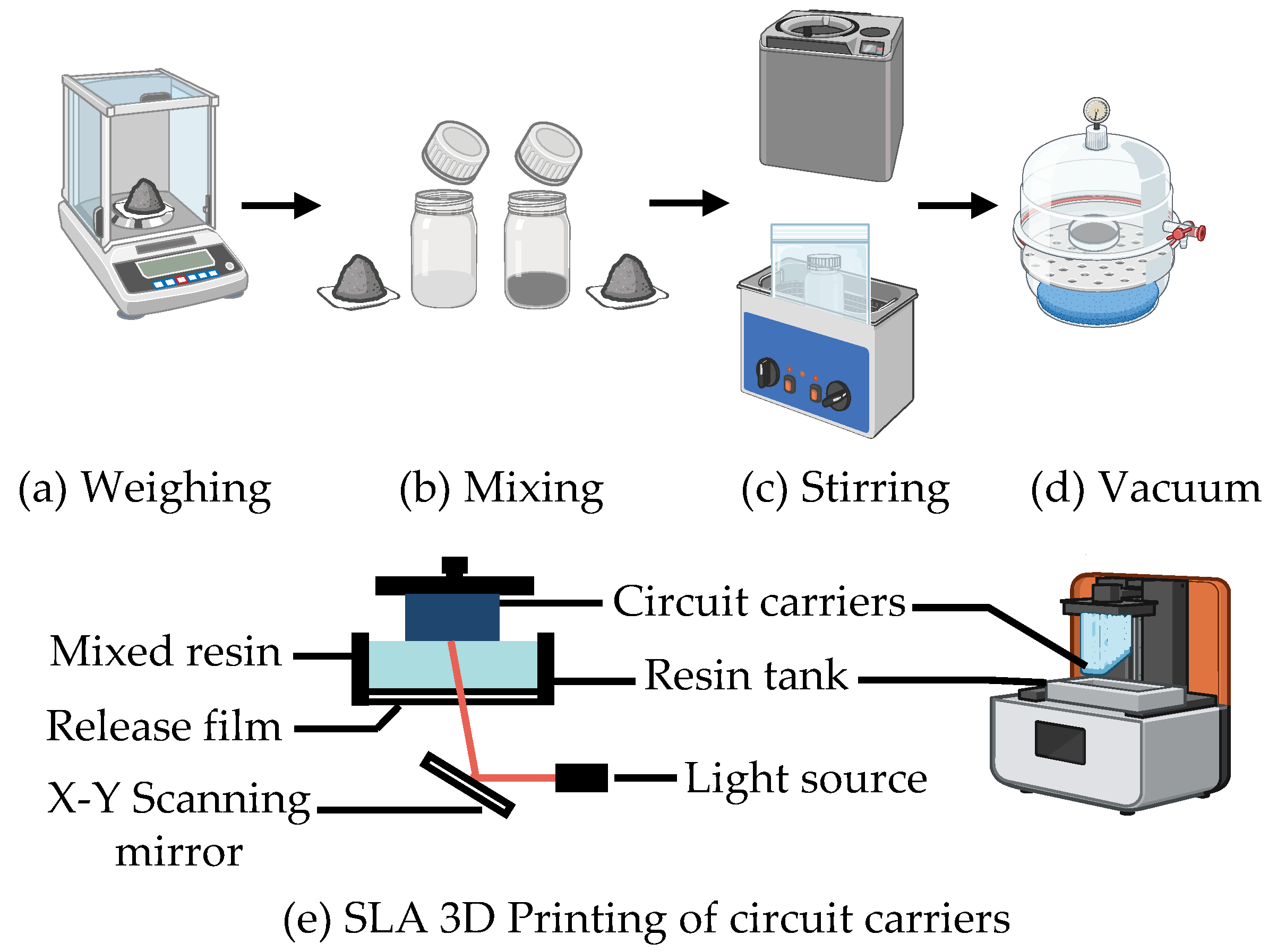
Figure 2.
The circuit board with U2 in a (a) QFN package and (b) BGA package. (c) Schematic diagram of the circuit board area.
Figure 2.
The circuit board with U2 in a (a) QFN package and (b) BGA package. (c) Schematic diagram of the circuit board area.
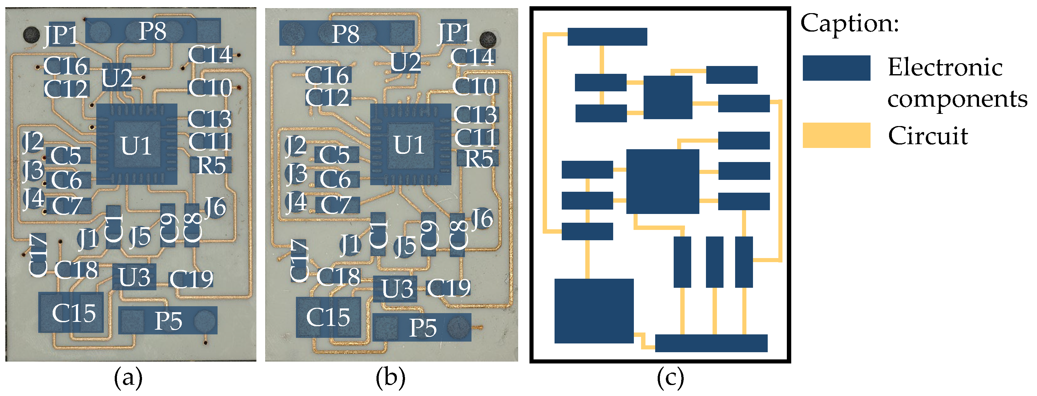
Figure 3.
Schematic representation of laser activation. [11]
Figure 3.
Schematic representation of laser activation. [11]
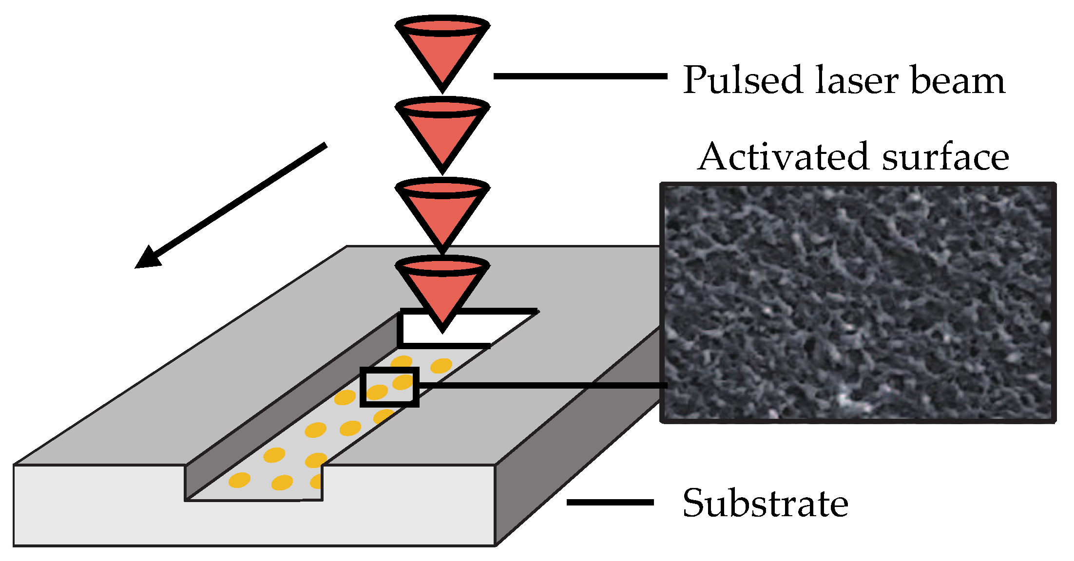
Figure 4.
Schematic diagram of the metallization process.
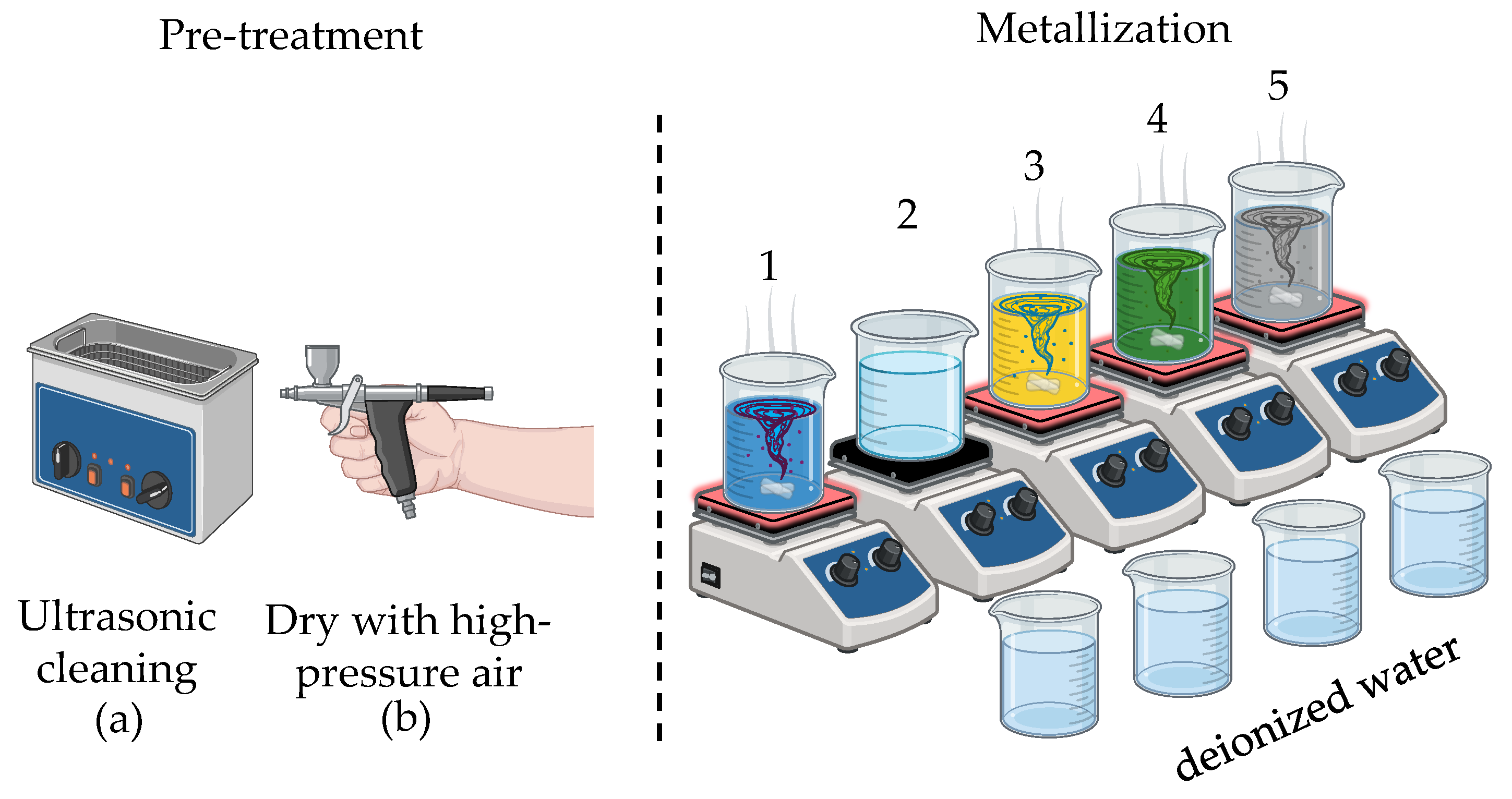
Figure 5.
Schematic Diagram of Sensor Circuit Carrier Dimensions.
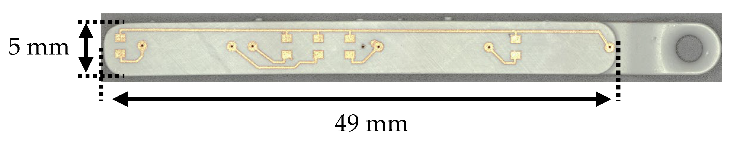
Figure 6.
Box Plot of the Impact of Different Post-Processing Methods on Circuit Carrier Dimensions.
Figure 6.
Box Plot of the Impact of Different Post-Processing Methods on Circuit Carrier Dimensions.
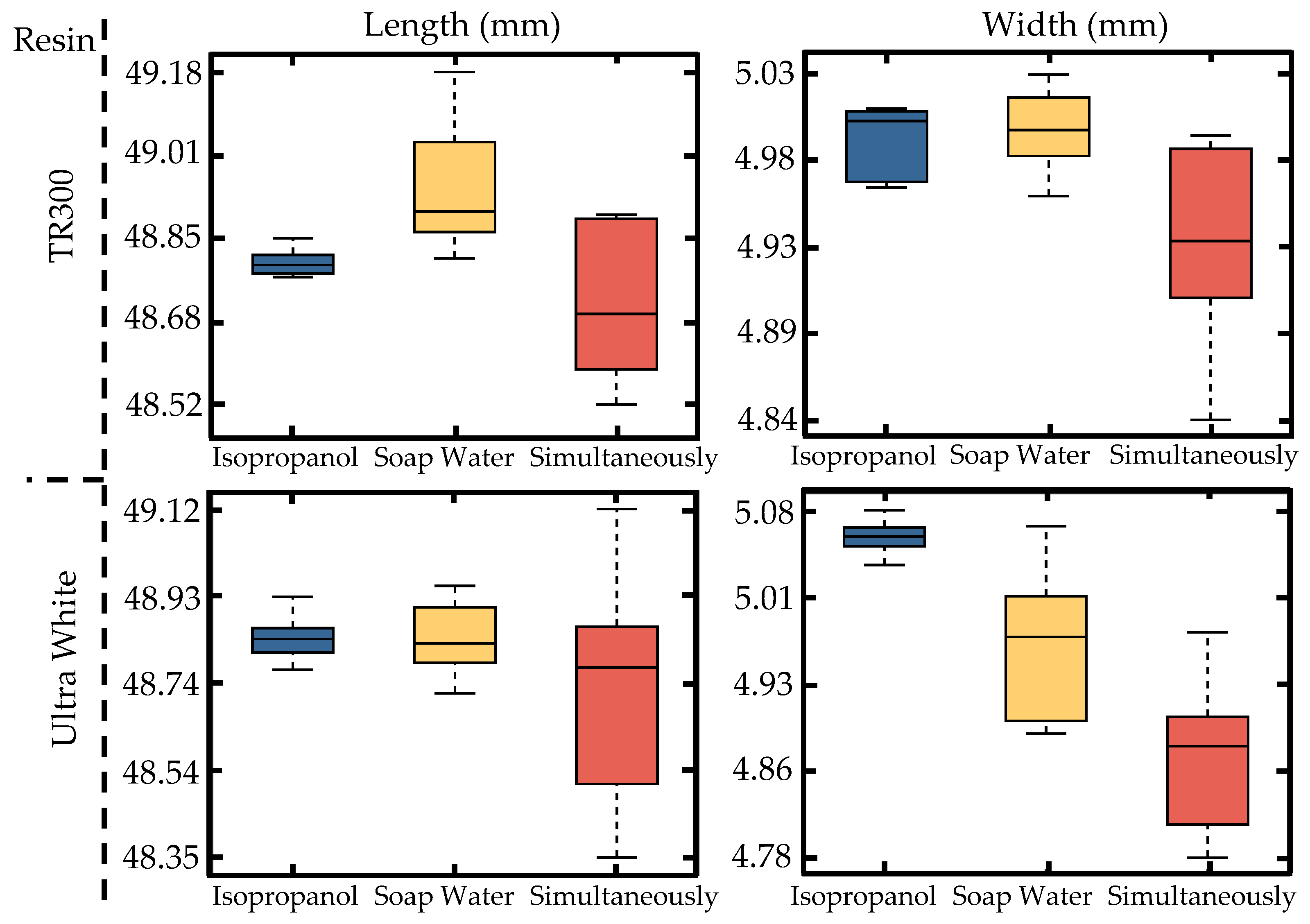
Figure 7.
Schematic Diagram of Via Hole in the Circuit Carrier.
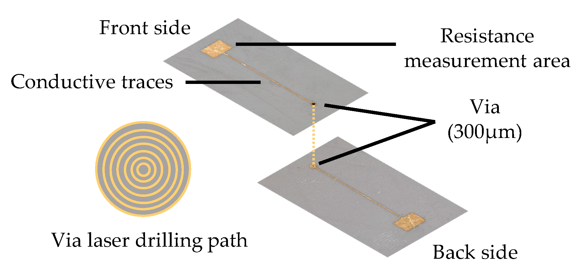
Figure 8.
Microscopic Close-Up of Via Holes in the Circuit.
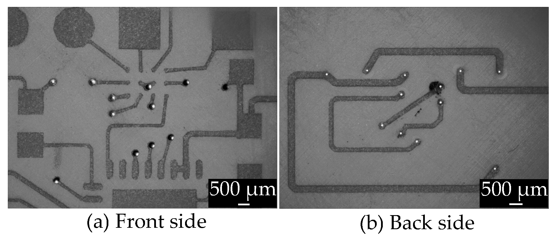
Figure 9.
Experimental Substrate with Via Holes for TR300 and UW.
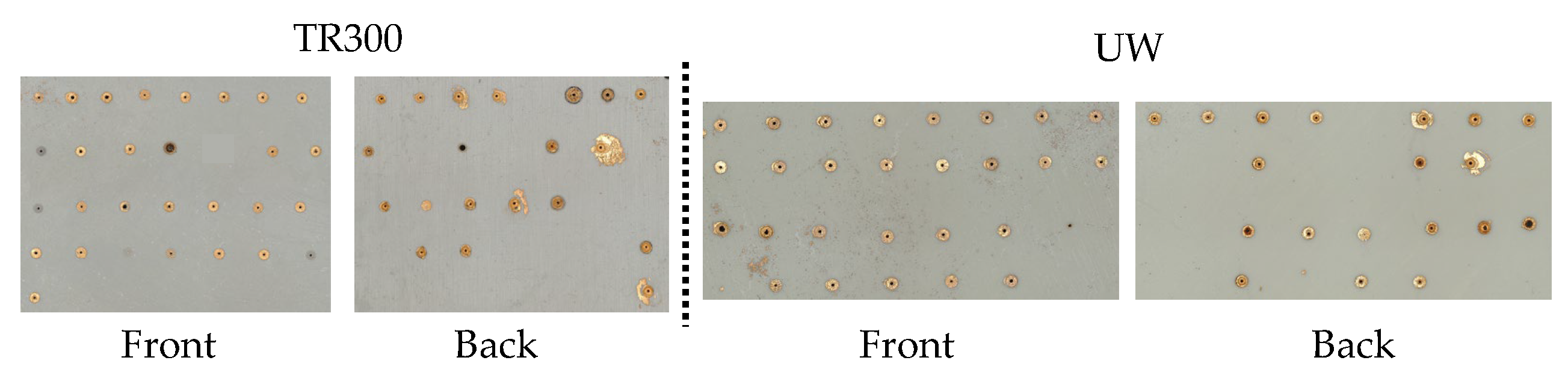
Figure 10.
Pareto Chart Analysis of Via Holes’ Resistances on TR300 Substrate.
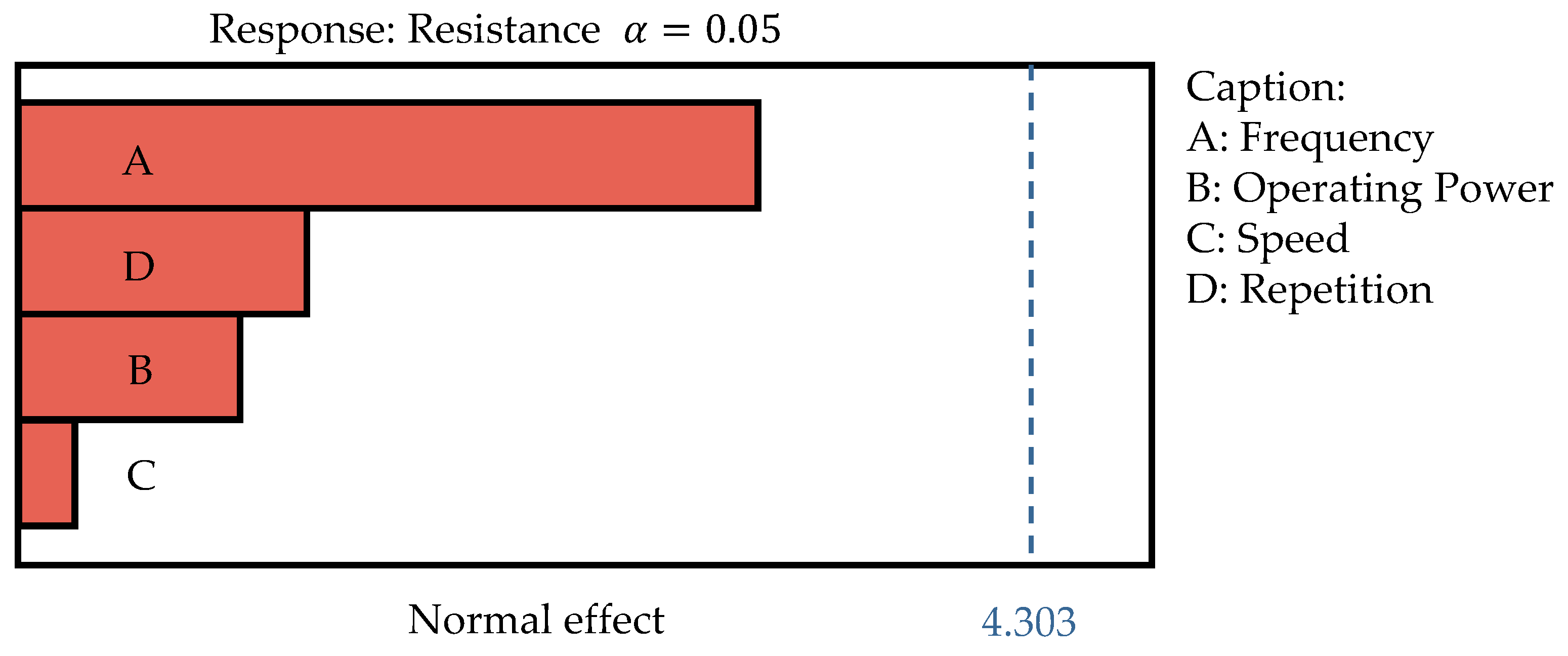
Figure 11.
(a) Via hole showing excessive metallization around the surrounding area; (b) Via hole showing no excessive metallization around the surrounding area.
Figure 11.
(a) Via hole showing excessive metallization around the surrounding area; (b) Via hole showing no excessive metallization around the surrounding area.
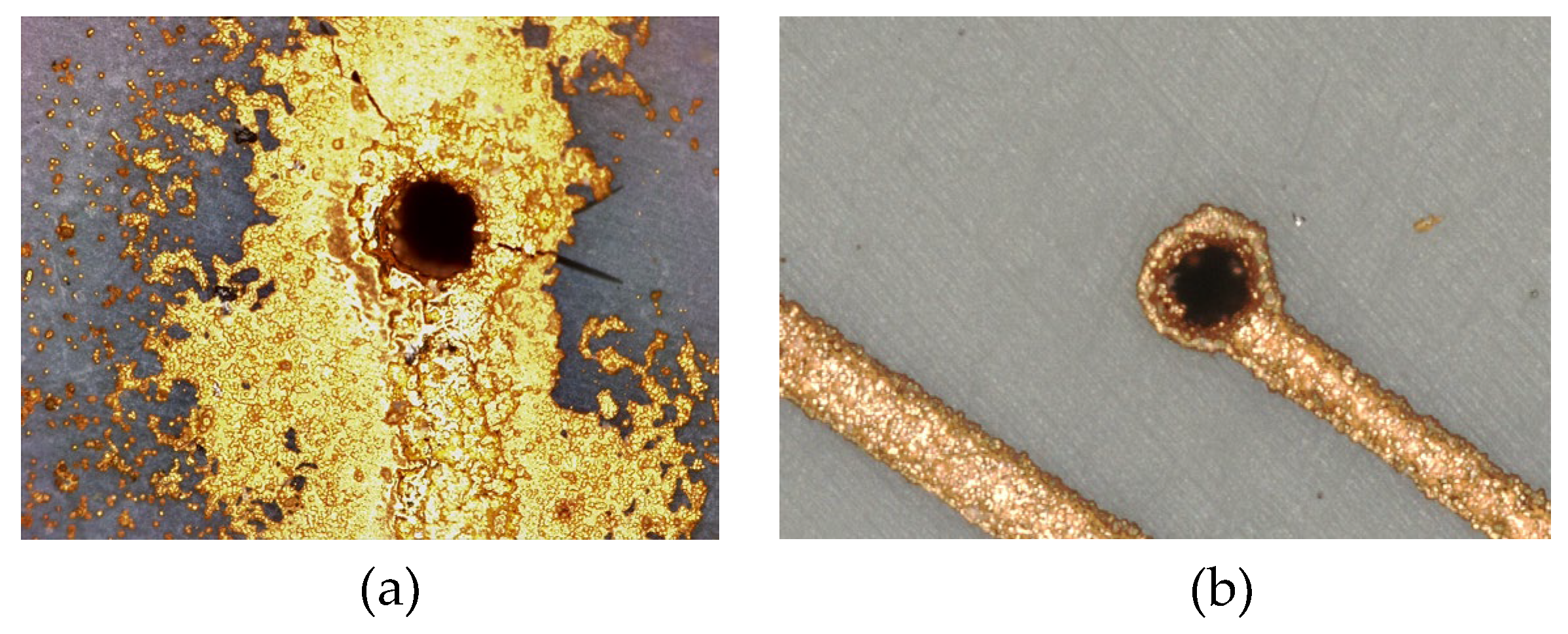
Figure 12.
Experimental Substrate with traces for TR300 and UW.
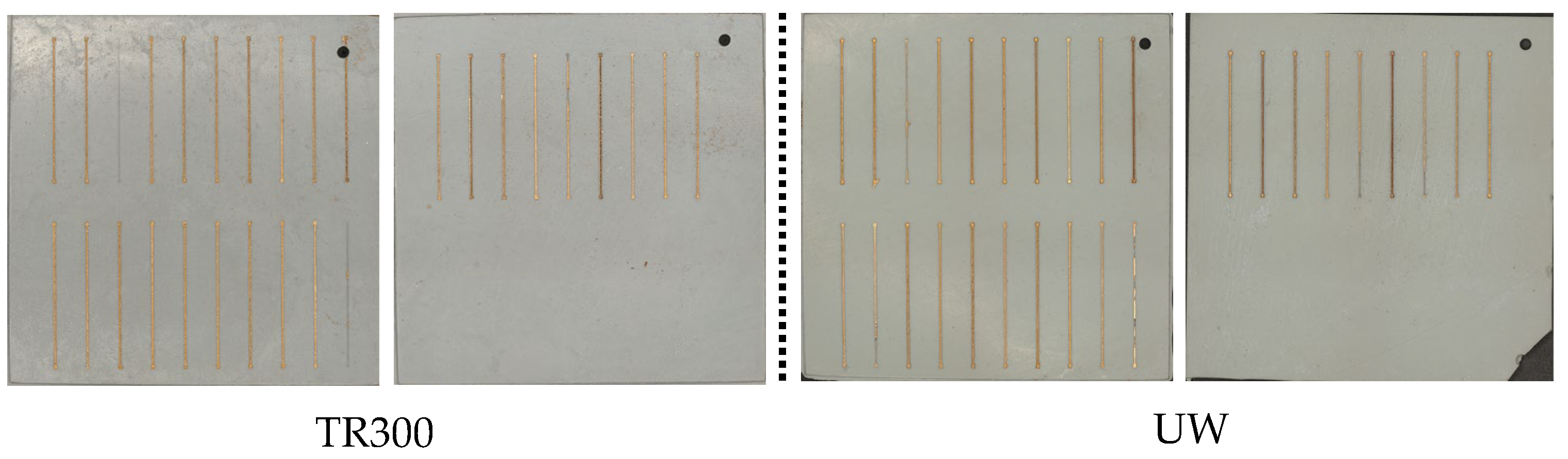
Figure 13.
3D Response Surface Plot of Resistance for Different Factors between TR300 and UW.
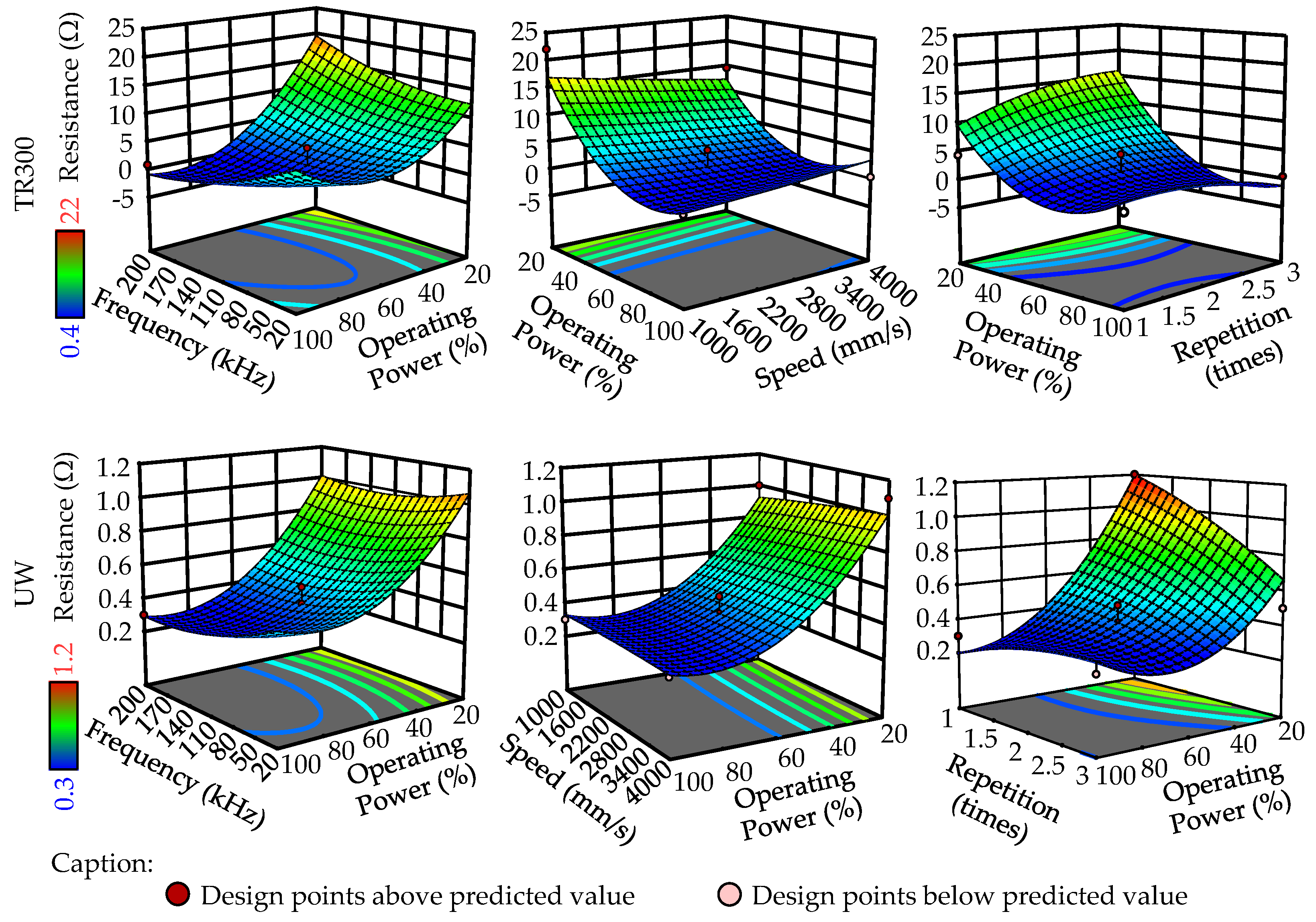
Figure 14.
(a) Perfect Circuit and (b) Over-metallized Circuit.
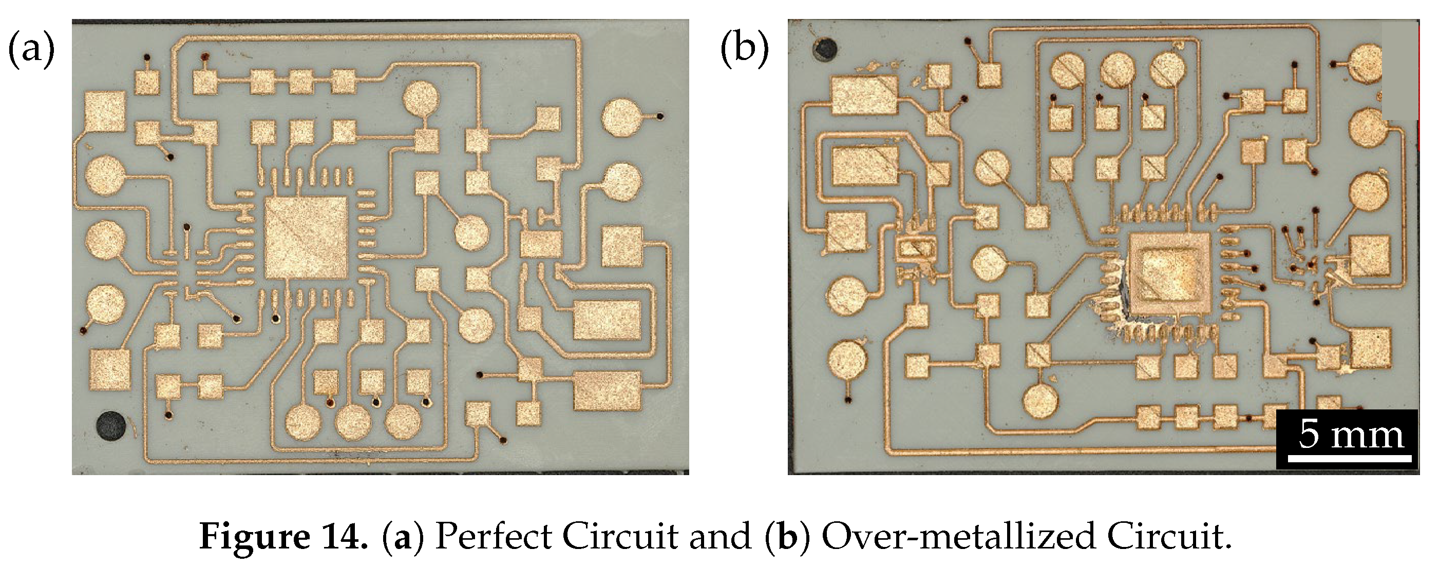
Figure 15.
Design of experimental structure for minimum circuit spacing.
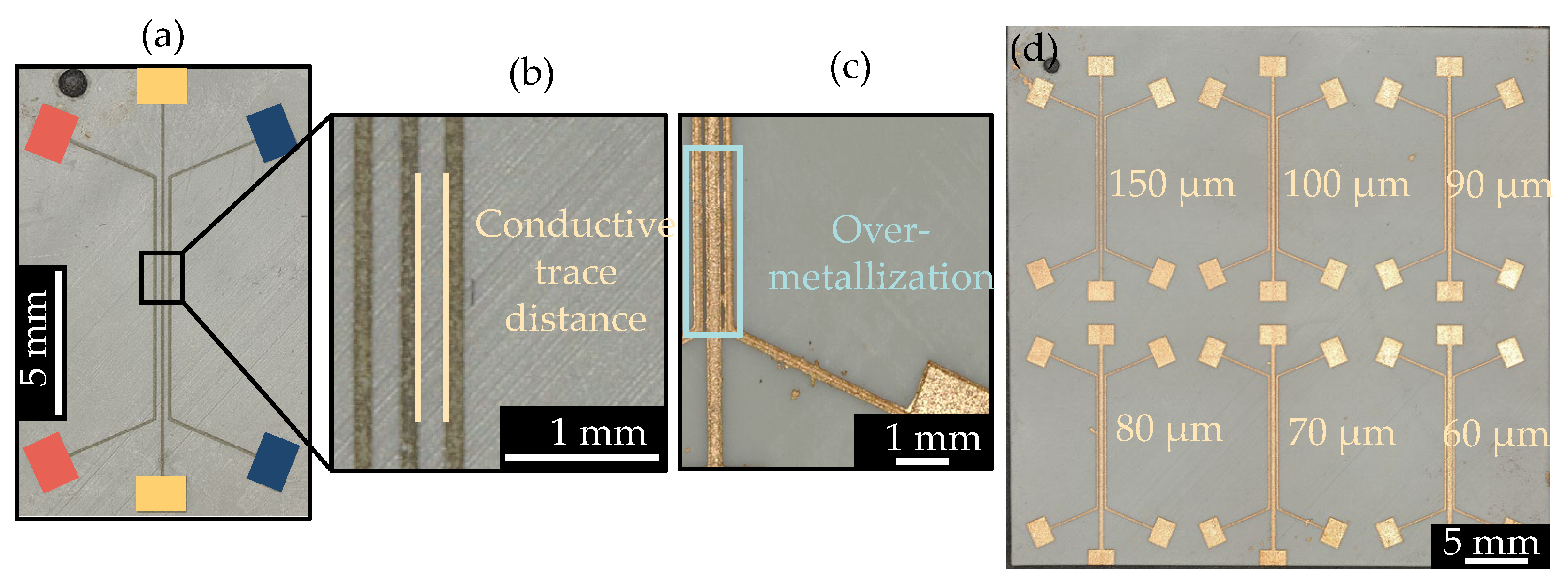
Figure 16.
The circuit on the (a) traditional circuit board and (b) SLA-printed Circuit Carrier.
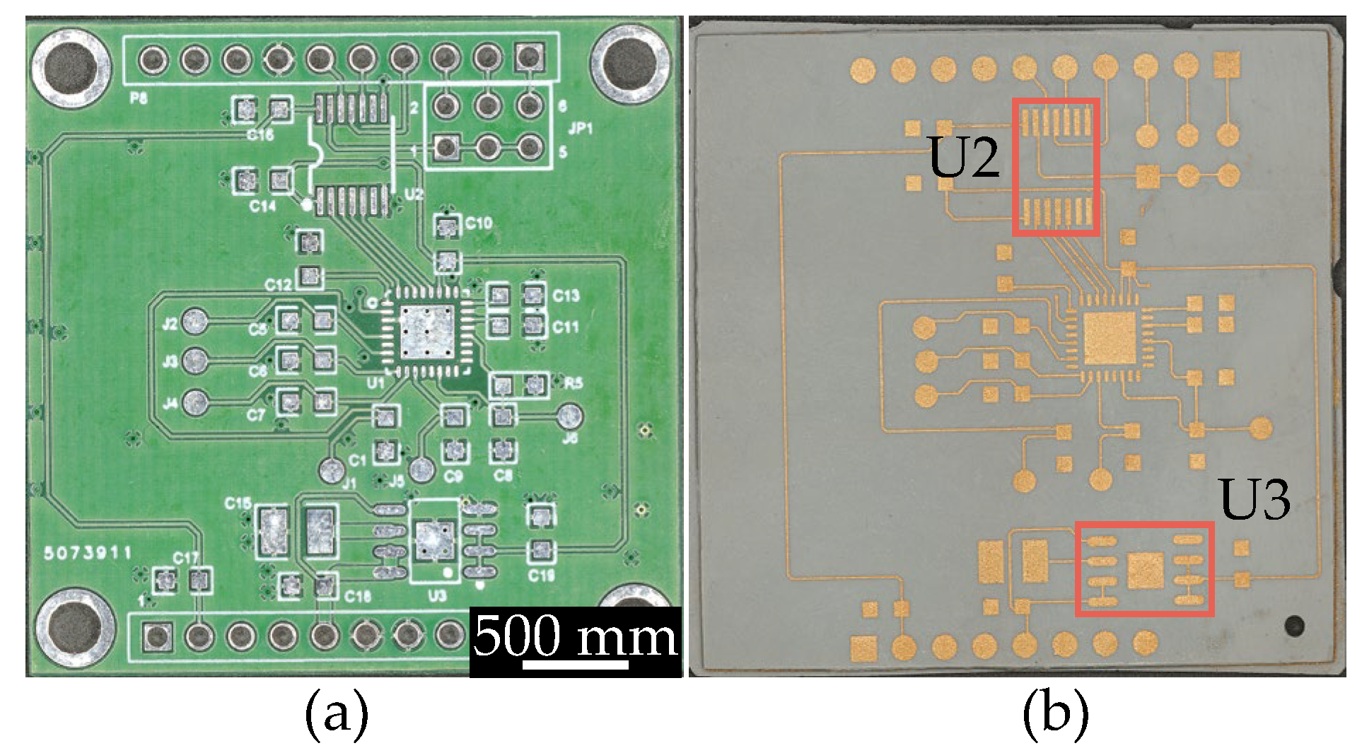
Figure 17.
The front (a) and back (b) views of the miniaturized circuit using a QFN package (UW), and the front (c) and back (d) views of the miniaturized circuit using a BGA package (TR300).
Figure 17.
The front (a) and back (b) views of the miniaturized circuit using a QFN package (UW), and the front (c) and back (d) views of the miniaturized circuit using a BGA package (TR300).
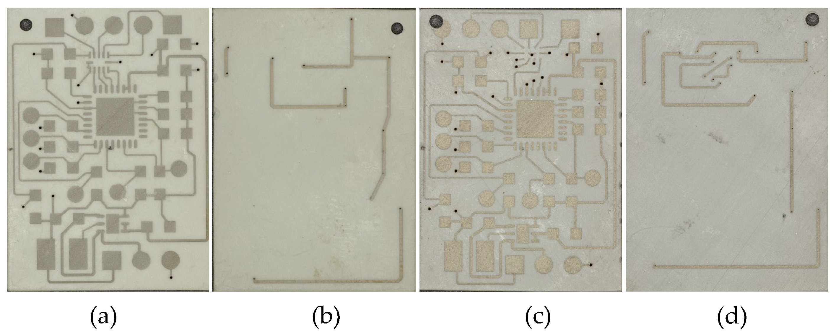
Figure 18.
Chip packages used in the original circuit and the miniaturized circuit.
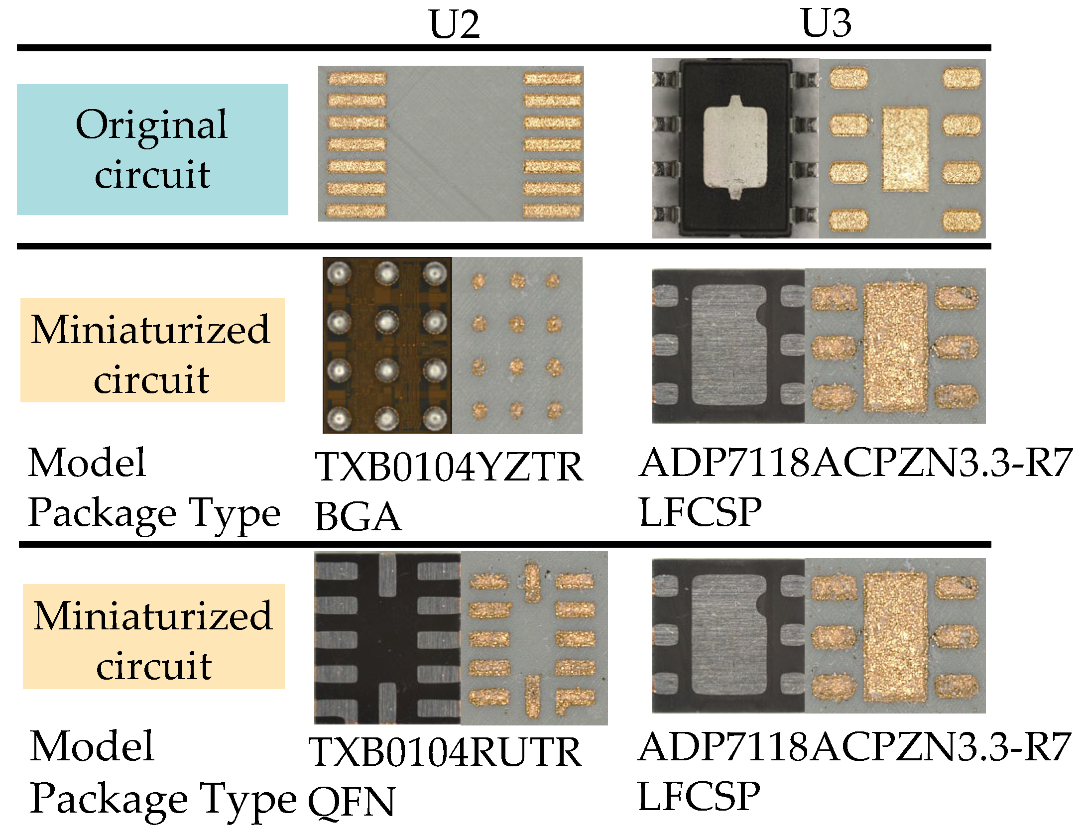
Figure 19.
(a) Solder paste stencil, (b) Circuit board with applied solder paste.
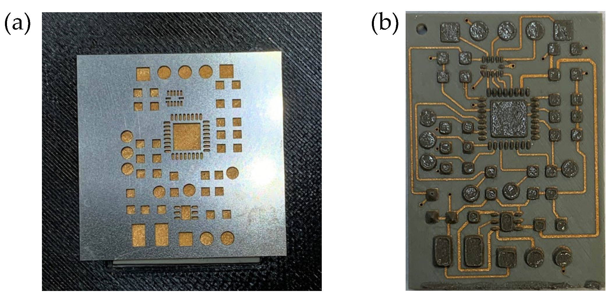
Figure 20.
(a) Cracks on the circuit board (Material: UW), (b) Flow of solder along the circuit.
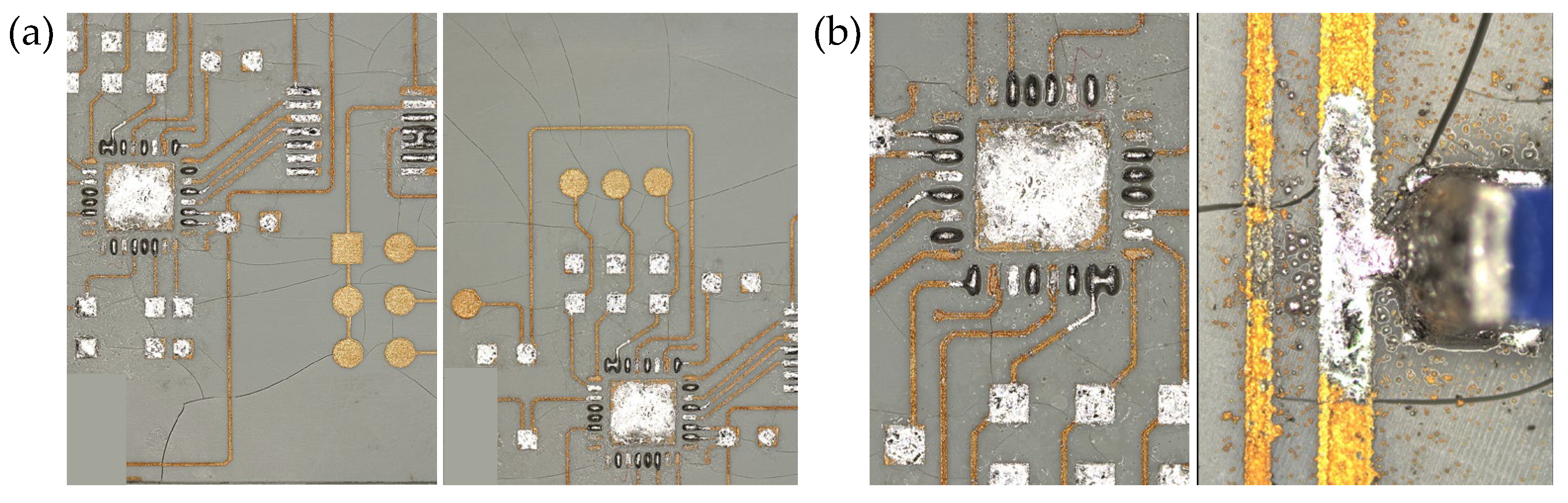
Figure 21.
The complete circuit board.
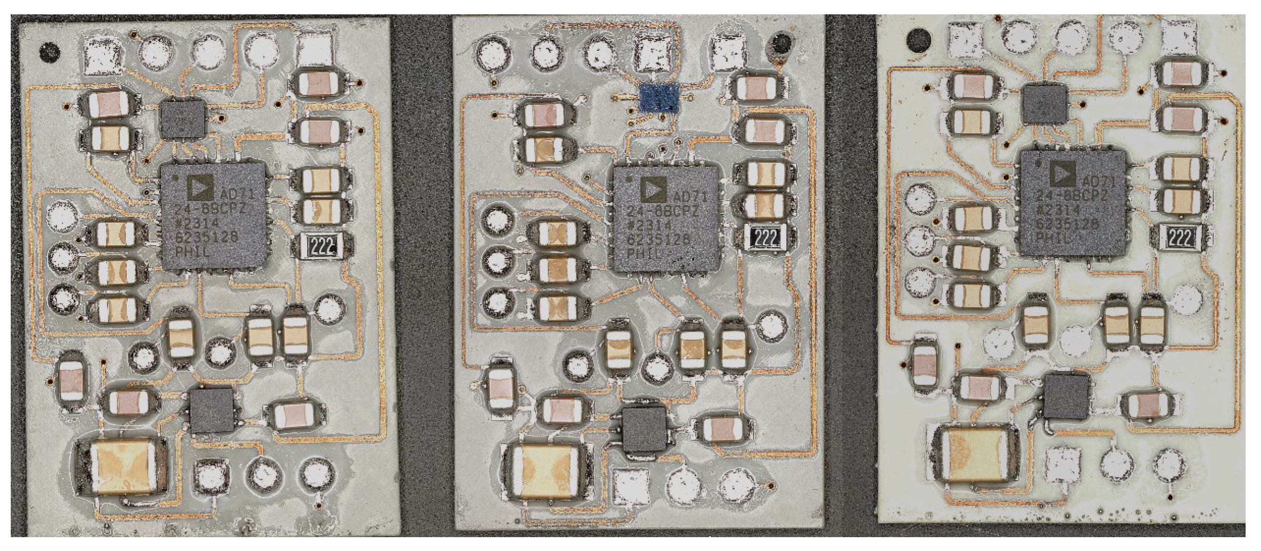
Figure 22.
(a) Schematic Diagram of 3D Pads, (b) Real-life Images of 3D Pads for Different Chips.
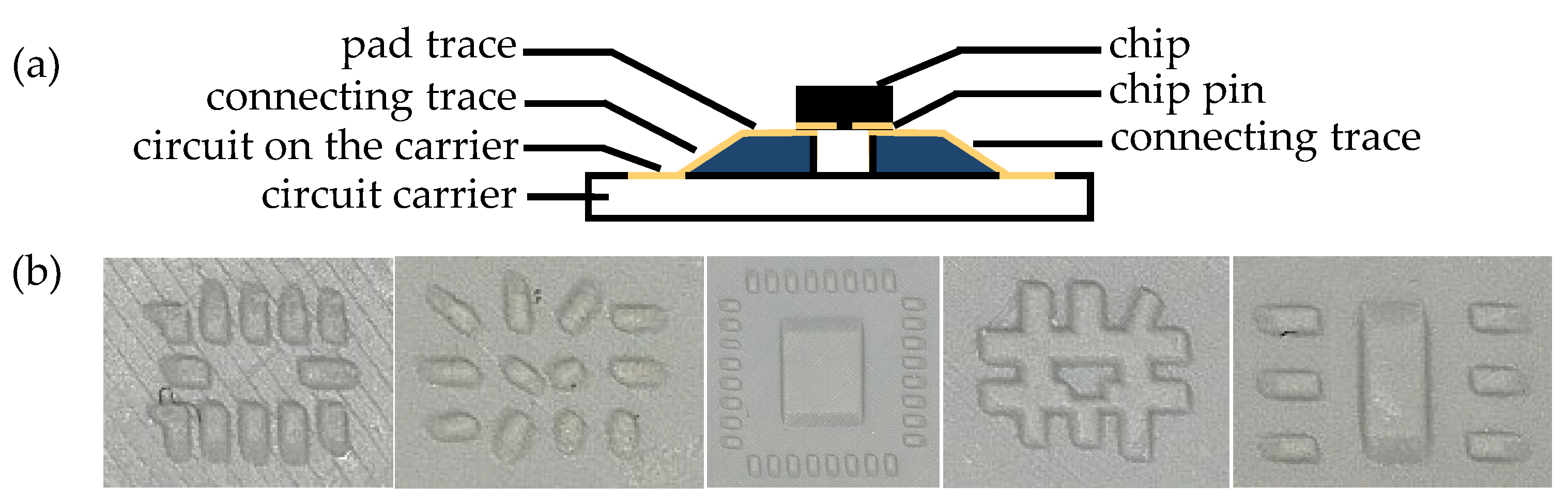
Figure 23.
Using 3D pads on circuits with (a) BGA /(b) QFN packaged chips.
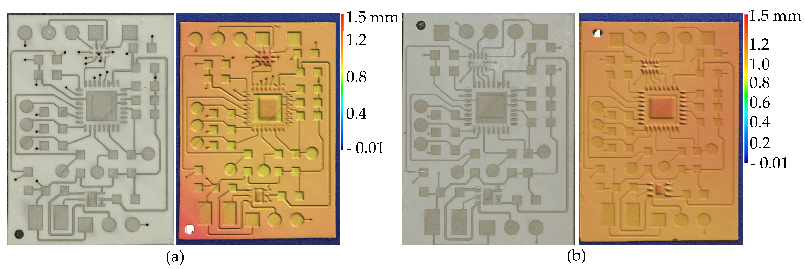
Figure 24.
(a) Wire connections on the SLA-MID circuit board, (b) Validation circuit (standard PCB board).
Figure 24.
(a) Wire connections on the SLA-MID circuit board, (b) Validation circuit (standard PCB board).
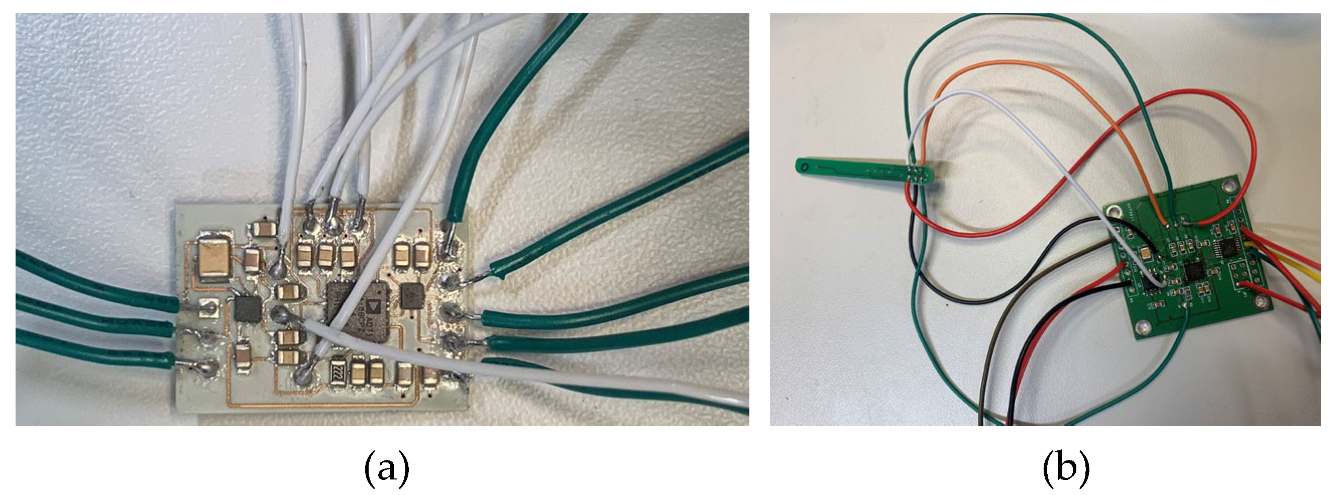
Figure 25.
X-ray scan of the resin circuit board.
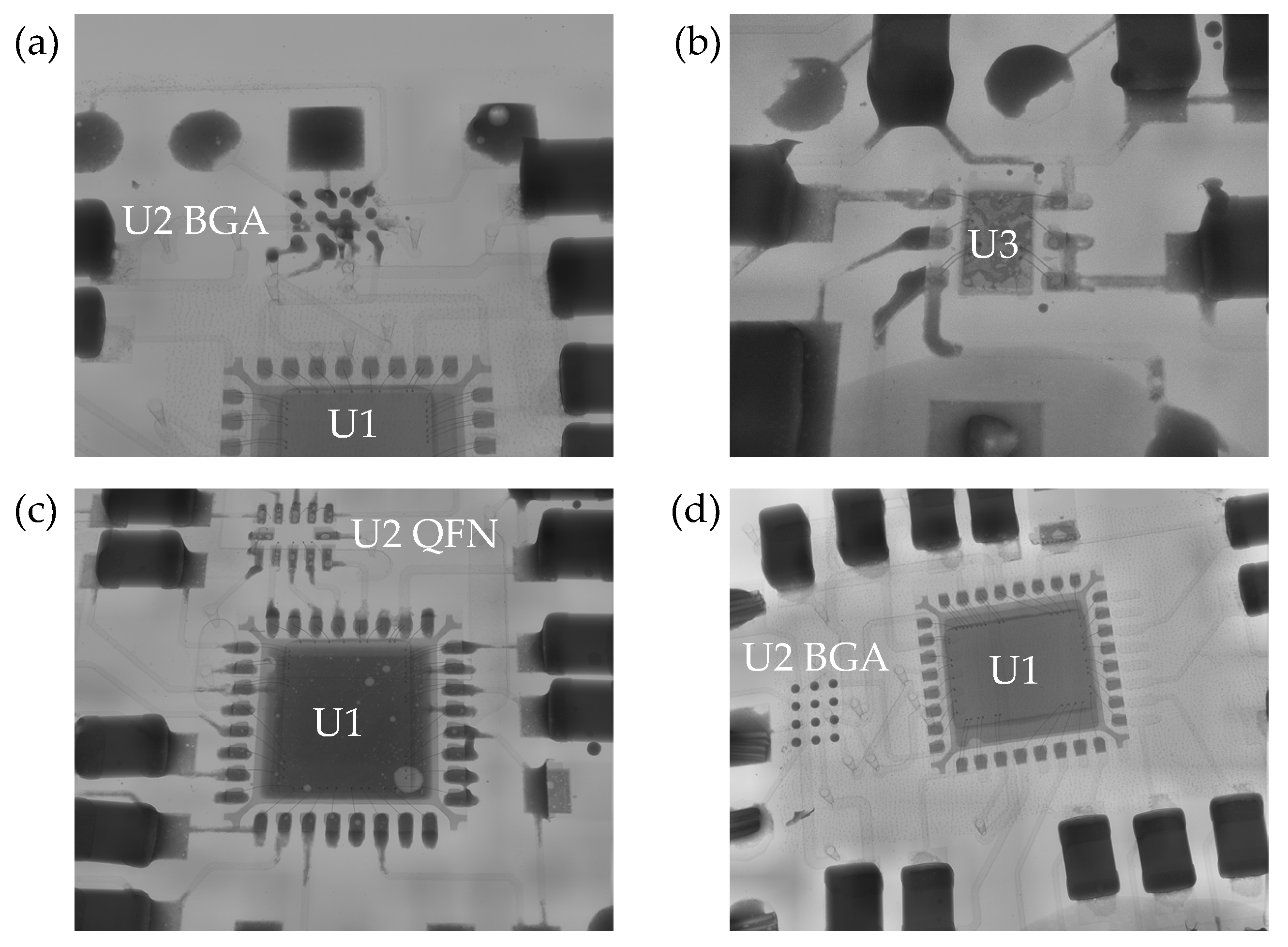

Table 1.
The Mixing Ratio and Stirring Method of the Resin.
| Resin | LDS Additives | Stirring Method |
|---|---|---|
| Phrozen TR300 (TR300) | 3% | Planetary Mixer and Ultrasonic Water Bath |
| Siraya Tech Ultra White (UW) | 3% | Planetary Mixer and Ultrasonic Water Bath |
Table 2.
First-Layer and Normal Layer Exposure Times for Mixed Resin.
| Resin | First-Layer (s) | Normal Layer (s) |
|---|---|---|
| TR300 | 75 | 1.2 |
| UW | 55 | 2.5 |
Table 3.
The names and areas of the electronic components.
| No. | Name | Area (mm2) |
|---|---|---|
| C1, C5 - C14, C16 - C19 | Capacitance | 3 |
| C15 | Capacitance | 11.9 |
| J1 - J6 | Measurement Point | 2.7 |
| R5 | Resistance | 3 |
| JP1 | - | 2.7 |
| P5 | Pin header | 11 |
| P8 | Pin header | 16 |
| U1 | Chip | 31.3 |
| U2 BGA/U2 QFN | Chip | 2/3.42 |
| U3 | Chip | 5 |
Table 4.
Summary of Metallization Process Operating Steps.
| Number in Fig. 8 | Solution | Temperature (∘C) | Time |
|---|---|---|---|
| 1 | Copper | 55 | 60 min |
| 2 | Acid | - | 30 s |
| 3 | Palladium | - | 1 min |
| 4 | Nickel | 62 | 60 min |
| 5 | Gold | 90 | 30 min |
Table 5.
Factors and Levels in the RSM Method (Via).
| Factor | Level |
|---|---|
| Frequency | 20, 110, 200 (kHz) |
| Operating Power | 20, 60, 100 (%) |
| Speed | 1000, 2500, 4000 (mm/s) |
| Repetition | 750, 825, 900 (times) |
Table 6.
ANOVA Analysis of Resistance Values of Via Holes on TR300 Substrate (Excerpt).
| Factor | Sum of Squares | df | Mean Square | F-Value | P-Value | |
|---|---|---|---|---|---|---|
| Model | 99.72 | 10 | 9.97 | 794.19 | <0.0001 | significant |
| Frequency | 0.0023 | 1 | 0.0023 | 0.1820 | 0.6845 | |
| Operating Power | 0.0310 | 1 | 0.0310 | 2.47 | 0.1670 | |
| Speed | 0.0023 | 1 | 0.0023 | 0.1820 | 0.6845 | |
| Repetition | 38.48 | 1 | 38.48 | 3064.79 | <0.0001 | |
| ... | ... | ... | ... | ... | ... | ... |
| Lack of Fit | 0.0633 | 2 | 0.0317 | 10.56 | 0.0254 | significant |
Table 7.
Laser Parameters for Via Holes on Both Resin Types.
| Frequency (kHz) | Operating Power (W) | Speed (mm/s) | Repetition (times) |
|---|---|---|---|
| 20 | 3.47 (100%) | 1500 | 900 |
Table 8.
Factors and Levels in the RSM Method (Circuit).
| Factor | Level |
|---|---|
| Frequency | 20, 110, 200 (kHz) |
| Operating Power | 20, 60, 100 (%) |
| Speed | 1000, 2500, 4000 (mm/s) |
| Repetition | 1, 2, 3 (times) |
Table 9.
ANOVA Analysis of Resistance Values of Circuits on TR300/UW (Excerpt).
| Factor | Sum of Squares | df | Mean Square | F-Value | P-Value | |
|---|---|---|---|---|---|---|
| Model | 627.22 | 14 | 44.8 | 3.93 | 0.0113 | significant |
| Model | 1.43 | 14 | 0.1019 | 11.08 | <0.0001 | significant |
| Frequency | 1.62 | 1 | 1.62 | 0.1423 | 0.7126 | |
| Frequency | 0.0313 | 1 | 0.0313 | 3.40 | 0.0901 | |
| Operating Power | 347.98 | 1 | 347.98 | 30.56 | 0.0001 | significant |
| Operating Power | 0.9425 | 1 | 0.9425 | 102.50 | <0.0001 | significant |
| Speed | 2.80 | 1 | 2.80 | 0.2462 | 0.6288 | |
| Speed | 0.0033 | 1 | 0.0033 | 0.3625 | 0.5583 | |
| Repetition | 8.17 | 1 | 8.17 | 0.7172 | 0.4136 | |
| Repetition | 0.1008 | 1 | 0.1008 | 10.97 | 0.0062 | |
| ... | ... | ... | ... | ... | ... | ... |
| Lack of Fit | 124.77 | 8 | 15.6 | 5.25 | 0.0633 | not significant |
| Lack of Fit | 0.0903 | 8 | 0.0113 | 2.26 | 0.2248 | not significant |
Table 10.
Laser Parameters for TR300 und UW.
| Frequency (kHz) | Operating Power (W) | Speed (mm/s) | Repetition (times) |
|---|---|---|---|
| 110 | 9.67 (60%) | 2500 | 1 |
| 110 | 9.67 (60%) | 2500 | 1 |
Table 11.
Model and Package Type of U2 and U3 in the Original Circuit.
| Chip | Model | Package Type |
|---|---|---|
| U2 | TXB0104PWR | TSSOP |
| U3 | ADP7156ARDZ-3.0-R7 | SOIC |
Table 12.
Soldering Methods and Principles.
| Machine | Principle | Material |
|---|---|---|
| IBL LC 280 | Condensation Soldering | TR300 |
| ERSA Hotflow 2/14 | Convection Soldering | TR300 and UW |
Disclaimer/Publisher’s Note: The statements, opinions and data contained in all publications are solely those of the individual author(s) and contributor(s) and not of MDPI and/or the editor(s). MDPI and/or the editor(s) disclaim responsibility for any injury to people or property resulting from any ideas, methods, instructions or products referred to in the content. |
© 2024 by the authors. Licensee MDPI, Basel, Switzerland. This article is an open access article distributed under the terms and conditions of the Creative Commons Attribution (CC BY) license (http://creativecommons.org/licenses/by/4.0/).
Copyright: This open access article is published under a Creative Commons CC BY 4.0 license, which permit the free download, distribution, and reuse, provided that the author and preprint are cited in any reuse.


