1. Introduction
In recent years, the field of artificial intelligence has witnessed remarkable advances driven by deep learning algorithms [
1,
2], particularly convolutional neural networks (CNNs) [
3], which have transformed visual recognition, natural language processing, and scientific computing. However, as CNN architectures continue to grow in complexity and depth, the computational burden associated with large-scale matrix multiplications and convolutional operations has become a major challenge for conventional electronic hardware such as graphics processing units and tensor processing units. Although these electronic accelerators achieve high throughput, they inherently suffer from latency caused by memory bandwidth limitations [
4], synchronization delays [
5], and significant power consumption [
6,
7]. These factors motivate the exploration of alternative computing paradigms that can achieve large-scale parallelism and energy efficiency [
8].
Optical computing has emerged as a compelling candidate to overcome the performance bottlenecks of electronic architectures. By leveraging the intrinsic parallelism and high bandwidth of light, optical convolutional neural networks (OCNNs) can, in principle, execute massive convolutional operations simultaneously at the speed of light. Traditional OCNNs often employ the 4f correlator configuration [
9,
10,
11,
12], which uses Fourier optics [
13] to perform spatial convolutions. While this architecture demonstrates impressive optical parallelism, it suffers from several well-known limitations, including the finite space–bandwidth product of lenses [
9], geometric aberrations, and slow refresh rates of spatial light modulators (SLMs). The limited update speed of SLMs, typically in the tens of kilohertz range [
14,
15], restricts the reconfigurability of such systems, making them unsuitable for dynamic or multilayer inference.
To address these constraints, free-space optical architectures utilizing lens arrays [
16] and Köhler illumination [
17,
18] have been proposed to achieve scalable optical CNNs (SOCNNs) [
19]. These architectures replaced the Fourier-domain filtering of 4f systems with direct spatial-domain convolution, allowing for unrestricted input dimensions and reduced crosstalk. However, the reliance on SLMs still imposed serious bottlenecks for weight updates, as each kernel reconfiguration required sequential pixel addressing. Consequently, the refresh rate of weights could not match the intrinsic optical processing speed, preventing true real-time adaptability.
The introduction of the smart-pixel-based optical convolutional neural network (SPOCNN) [
20] represented a major step forward. In this architecture, the conventional SLM was replaced by a smart pixel light modulator (SPLM) [
21,
22] that integrates a photodetector, electronic processor (EP), and light-emitting diode (LED) within each pixel. This hybrid optoelectronic design enables localized optical–electrical–optical conversion, permitting ultrafast modulation and weight updates in the hundreds of megahertz range. The EP within each smart pixel performs analog multiplication of incoming optical signals with stored weights, while the output light intensity corresponds to the weighted result. This innovation allows SPOCNNs to maintain the inherent optical parallelism of free-space systems while adding programmability and fast reconfigurability.
Further evolution led to the development of the smart-pixel-based bidirectional optical convolutional neural network (SPBOCNN) [
20], which extended SPOCNNs by enabling light propagation in both forward and backward directions through the same physical space. This bidirectionality opened the possibility of implementing training-related algorithms such as error backpropagation directly in optical hardware. By integrating electrical fan-in and fan-out structures, SPBOCNNs reduced wiring complexity and enhanced hardware modularity. Additionally, their bidirectional operation facilitated the realization of two-mirror-like architectures capable of emulating multiple neural layers using only two physical layers—significantly reducing hardware volume while retaining computational capacity.
Despite these advances, prior SPBOCNN implementations remained optically asymmetric: the forward and backward paths required separate optical alignments and distinct substrate arrangements for photodetectors and light sources. This asymmetry complicated optical alignment, increased packaging difficulty, and led to higher fabrication costs. To overcome these challenges, this work introduces a symmetric smart-pixel-based bidirectional optical convolutional neural network (Sym-SPBOCNN). The proposed system introduces a geometrically symmetric optical configuration in which the forward and backward light paths share identical lens arrangements and distances. Such symmetry not only simplifies optical design and alignment but also ensures identical optical characteristics in both propagation directions, enabling stable and efficient bidirectional computation.
The Sym-SPBOCNN architecture employs two identical SPOCNN modules arranged side by side to handle forward and backward propagation. The optical convolution operation is performed through lens arrays that project weighted light distributions from one SPLM plane to the opposite plane. Because of the symmetric layout, the same optical elements process both forward inference and backward computation, allowing the development of a single optical system for both directions. This design also simplifies the SPLM structure, since each SPLM requires only a light-source array on the top surface instead of separate light-source and detector arrays for bidirectional communication.
These features greatly reduce development steps and manufacturing effort, leading to lower production costs and easier system integration using a well-established lens-array imaging platform. Collectively, these characteristics position the Sym-SPBOCNN as an efficient and reconfigurable computing architecture that bridges the gap between optical speed and electronic adaptability.
The remainder of this paper is organized as follows.
Section 2 presents the theoretical model and optical configuration of the proposed symmetrical bidirectional architecture.
Section 3 analyzes the optical characteristics, scalability, system throughput, and comparisons with previous SPBOCNN systems.
Section 4 discusses the application of crossbar switches to the Sym-SPBOCNN for implementing a two-mirror-like architecture and examines the feasibility of the proposed system. Finally,
Section 5 summarizes the conclusions and outlines future directions for developing practical, large-scale symmetrical optical neural networks based on smart-pixel technology.
2. Materials and Methods
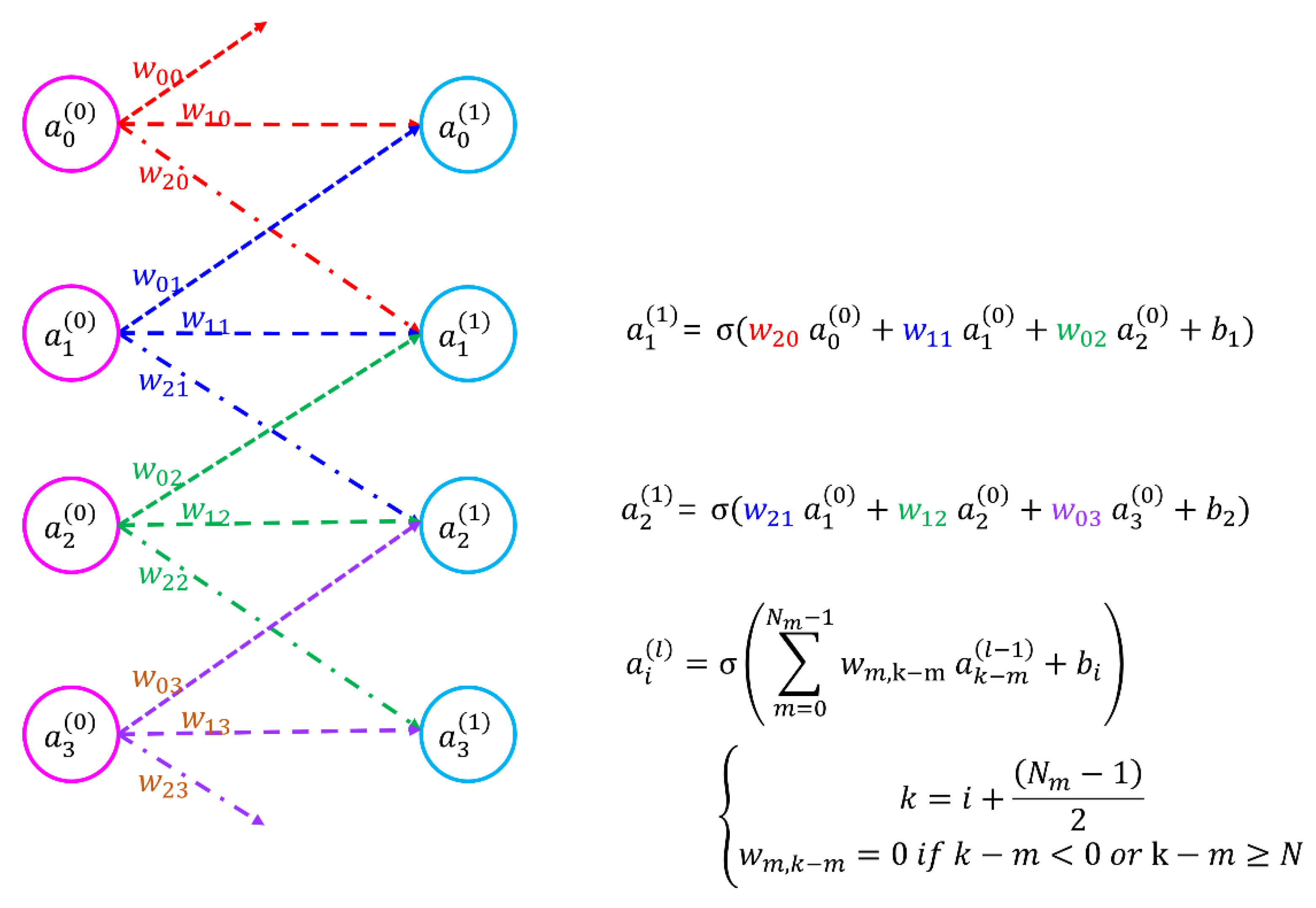
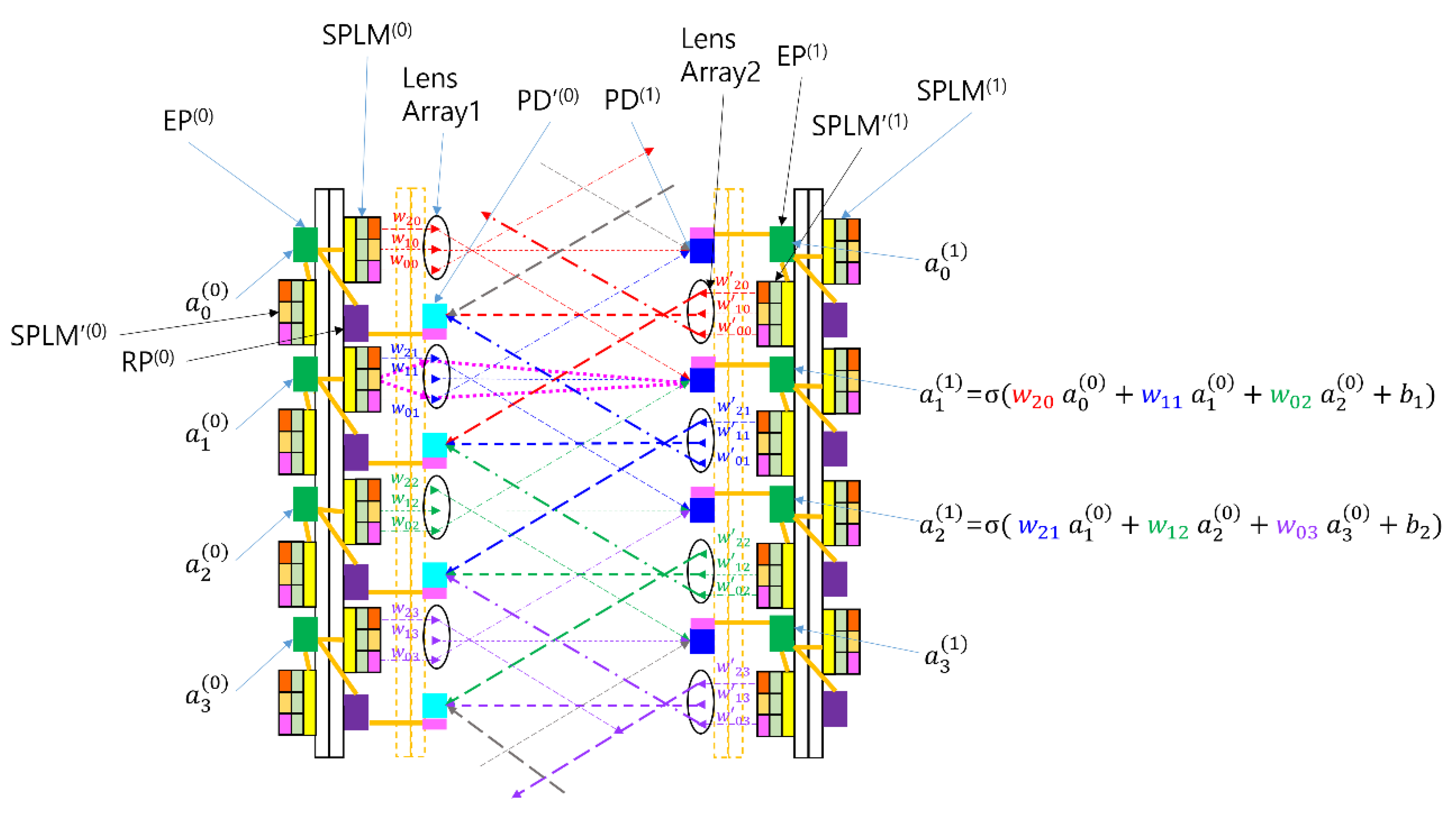
Before discussing the architecture of the proposed Sym-SPBOCNN, we briefly revisit the core concept of a CNN and SPBOCNN. As shown in
Figure 1 and detailed in our earlier study [
19], a CNN consists of input and output neurons linked by weighted local connections. During inference, the signals from the input nodes are transmitted through these weighted links to produce outputs. In contrast to fully connected optical neural networks such as linear combination optical engine (LCOE) [
23], CNNs rely on partial or spatially constrained connectivity, where the learnable weights form convolution kernels.
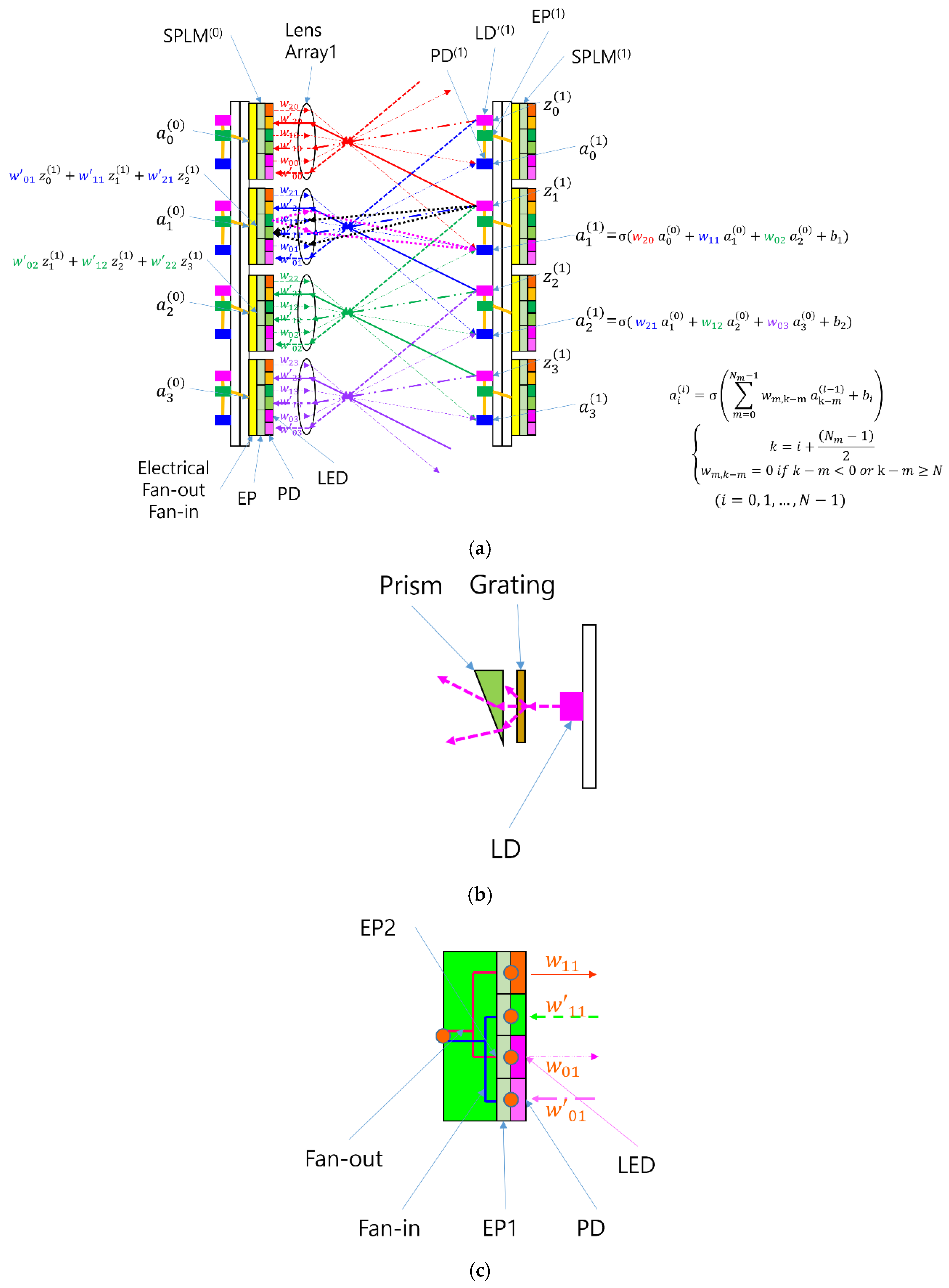
The CNN concept is implemented in the SPBOCNN architecture, as shown in
Figure 2(a), with additional functional details provided in [
20]. A distinctive aspect of this architecture is its bidirectional communication capability, made possible by the integration of backward light sources, SPLM arrays, and lens arrays. In particular, the backward light source utilizes a diffraction grating and prism, as depicted in
Figure 2(b), to distribute optical signals toward the SPLM array on the opposite substrate. The optical signals arriving at SPLM
(0) pixels from multiple LD′
(1) emitters are then summed through an electrical fan-in circuit, as illustrated in
Figure 2(c). This bidirectional optical routing forms the foundation of the SPBOCNN’s convolutional connectivity.
The SPBOCNN further enhances this architecture by employing SPLMs capable of modulation speeds in the hundreds of megahertz, with embedded EP memory enabling nanosecond-scale weight updates. This high-speed reconfigurability eliminates the major performance limitation of earlier BONN systems that relied on slower SLM technologies. As a result, real-time hardware implementation of backpropagation becomes feasible. Moreover, the bidirectional signal propagation and rapid in-pixel weight updating allow the two-mirror-like SPBOCNN (TML-SPBOCNN) [
20] architecture to emulate deep, multilayer networks using only two physical layers. Information reciprocates between the two layers, enabling scalable depth without additional optical hardware—made possible by the memory-integrated smart pixels of the SPLM.
To maintain bidirectional computation within a compact footprint, each SPLM pixel is partitioned into forward and backward modulation units, enabling both propagation directions within the same device. Additional simplification is achieved by integrating electrical fan-in for backward-signal summation and consolidating optical components such as lenses. These refinements reduce optical alignment sensitivity, shrink system size, and improve implementation practicality.
The SPBOCNN architecture Is Inherently scalable, enabling multiple layers to be cascaded to increase computational depth and throughput for continuous data processing. Each layer comprises a smart-pixel array, a lens array, and a detector array arranged to support bidirectional signal flow. As a result, SPBOCNN offers a compact, high-speed, and flexible optical computing platform capable of efficient convolutional processing with dynamic weight updates.
However, earlier SPBOCNN designs still exhibited a key limitation: the bidirectional operation relied on asymmetric optics, requiring separate alignment procedures and distinct substrate layouts for the forward and backward directions. This structural asymmetry introduced considerable complexity in alignment and packaging, ultimately increasing fabrication and assembly costs.
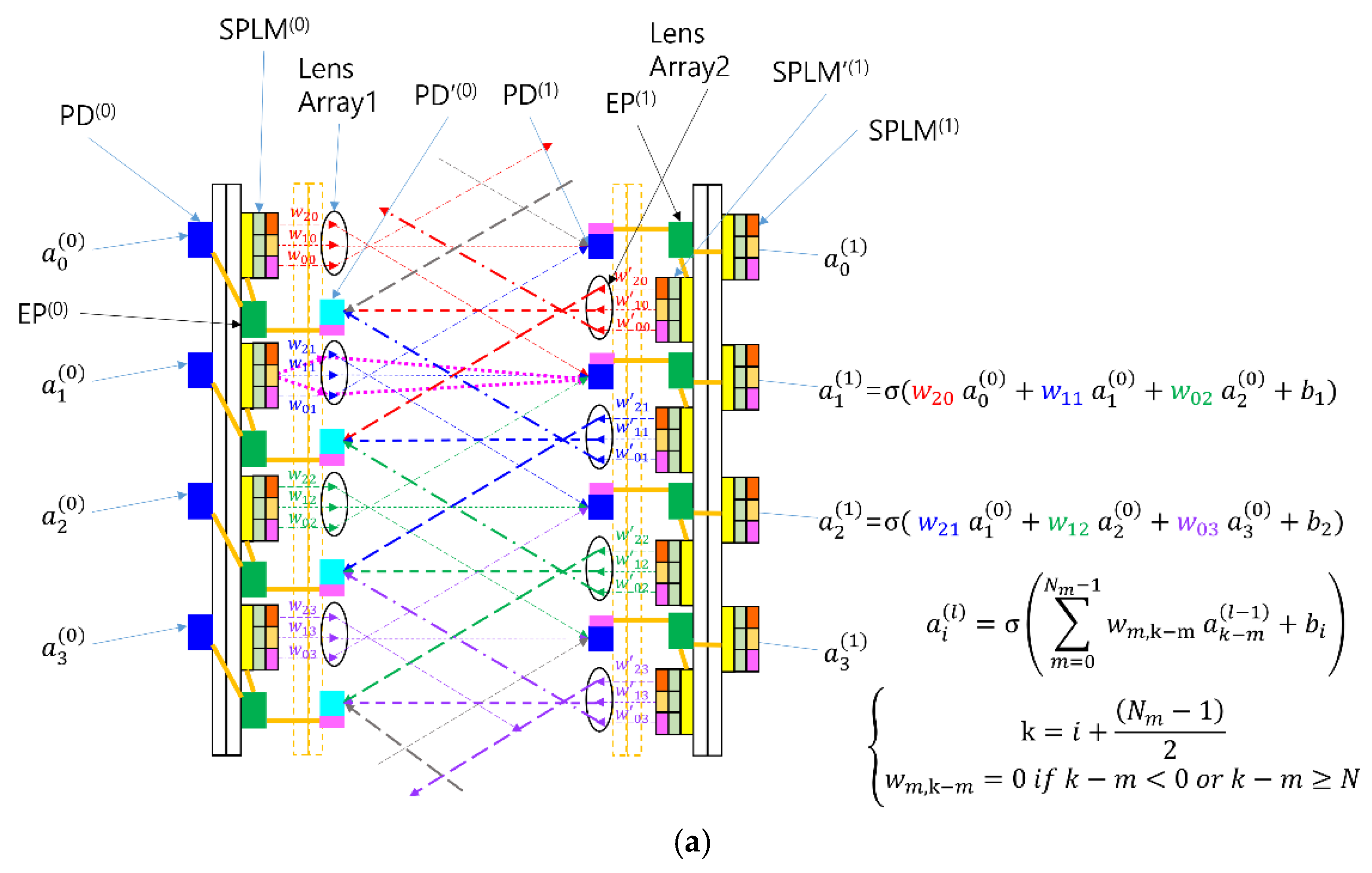
To overcome these limitations, we propose a symmetric optical configuration for both forward and backward propagation, as illustrated in
Figure 3. Two identical optical paths are placed side by side: one dedicated to forward propagation and the other to backward propagation. Each path incorporates an SPLM, a lens, and a detector on the opposite side. Notably, the SPLM in this configuration supports only outgoing light modulation, differing from the bidirectional SPLM used in the SPBOCNN. This type of unidirectional SPLM has previously been demonstrated in our earlier work [
20]. As shown in
Figure 3b, it integrates light emitters such as micro-LEDs [
24] or vertical-cavity surface-emitting lasers (VCSELs) [
25] above the EP layer and employs an electrical fan-out for routing signals. Because the device no longer requires a photodiode (PD) on the topmost layer—as is the case in the SPBOCNN—its fabrication becomes simpler and more cost-effective.
A practical implementation example of this unidirectional SPLM is illustrated in
Figure 3c. Here, the EP chip is bonded to a silicon submount that provides electrical fan-out, and the VCSEL array is attached to the EP chip using micro-bump bonding, a well-established technique in modern 3D chip packaging.
Figure 3d presents a three-dimensional view of the Sym-SPBOCNN architecture.
3. Results
The Sym-SPBOCNN inherits the optical characteristics of the SPBOCNN, with the key distinction that its forward and backward channels are interlaced side by side. In the original SPBOCNN, the SPLM modules are arranged with a spacing of
b on the zeroth substrate, while the PDs are placed with the same spacing
b on the opposing first substrate. In contrast, the Sym-SPBOCNN interlaces both SPLM modules and PDs with a spacing of
, as shown in
Figure 3d. The opposite substrate follows the same pattern, except that an SPLM on the zeroth substrate faces a PD on the first substrate and vice versa. In the square-lattice arrangement with a period of
b, two opposite corners are occupied by SPLM modules, and the remaining two corners are occupied by PDs.
This symmetric arrangement of optical components allows the scaling behavior of the Sym-SPBOCNN to be analyzed using parallels to the SPBOCNN [
20] or SOCNN [
19] models. One major difference lies in the fill factor of the light source within each pixel. As illustrated in
Figure 3d, the light-source size (e.g., micro-LED or VCSEL) is assumed to be
ε, whereas the spacing between neighboring pixels is
. This spacing is larger by a factor of
compared with SOCNN, where adjacent pixels are separated by
d. This configuration can be interpreted as effectively removing every other pixel in a densely packed SOCNN-style array with spacing
d. Therefore, if the scaling limit of the kernel size in SOCNN is 66 × 66, then in the Sym-SPBOCNN architecture it becomes
, since half of the pixel positions are unavailable or reserved for the opposite-direction data flow.
Regarding the optical setup, the pixel array on the zeroth substrate is imaged onto the first substrate by Lens1, while the pixels on the first substrate are imaged onto the zeroth substrate by Lens2. Because the spacing between the pixels on the zeroth substrate must be magnified to match the spacing between the detectors on the first substrate, the required magnification factor M becomes , which is also expressed as .
Building on earlier scaling studies [
19,
20], the magnification factor
M in the proposed system can theoretically reach values up to 46, which is sufficiently large for practical Sym-SPBOCNN implementations. This array-size limit of 46×46 assumes an f/# of 2 for Lens1 and an angular aberration of approximately 3 mrad. Nonetheless, this theoretical bound can be extended by employing LCOE architectures with clustering techniques [
23] or smart-pixel based optical neural network (SPONN) systems coupled with software-based scaling strategies [
20]. Whereas Sym-SPBOCNN provides only partial connectivity between its input and output arrays, both LCOE and SPONN architectures enable fully connected mappings. In this sense, the interconnections in Sym-SPBOCNN represent a subset of those available in LCOE or SPONN, implying that SPONN can emulate a Sym-SPBOCNN configuration with matching input and output sizes. Because fully connected optical neural networks can scale effectively through clustering and the use of smart-pixel memory, the inherent limitations of the Sym-SPBOCNN can be substantially mitigated.
The performance analysis follows a similar approach to that of the SPBOCNN [
20], as the bidirectional optical paths of the Sym-SPBOCNN share the same structural configuration as the forward path in SPBOCNN. Consequently, the parallel processing capability of the Sym-SPBOCNN is largely dictated by the size of the SPLM array. The SPLM can be divided into smaller subarrays according to the kernel size; using smaller kernels increases the portion of the SPLM available for the input array. The device can also be segmented so that multiple kernels are processed simultaneously by replicating the input pattern across different regions. Each region can independently execute convolution operations with distinct kernels in parallel.
Within the Sym-SPBOCNN, however, multiple kernels can also be handled sequentially through the SPLM’s built-in memory, removing the need for dedicated optical channels for each kernel set. Under this configuration, the number of operations per cycle equals half the number of pixels on the SPLM. For an SPLM with a resolution of 3840 × 2160, this corresponds to approximately 4.1×10
6 effective connections, enabling the same number of multiply-and-accumulate (MAC) operations per cycle. If electronic processing dominates the system latency (about 10 ns [
22]), the resulting computational throughput reaches 4.1×10
14 MAC/s. Although the SPLM may introduce a comparable delay of approximately 10 ns, kernel updates can be performed concurrently with signal processing at the detector-plane smart pixels under continuous-input operation, thus avoiding additional cycle overhead.
Throughput can be further increased by adding more processing layers. While additional layers introduce extra propagation delay, each layer operates concurrently in a pipeline-like manner, similar to multi-stage digital processing. With ten layers operating in parallel, the overall system throughput can reach approximately 4.1×10¹⁵ MAC/s.
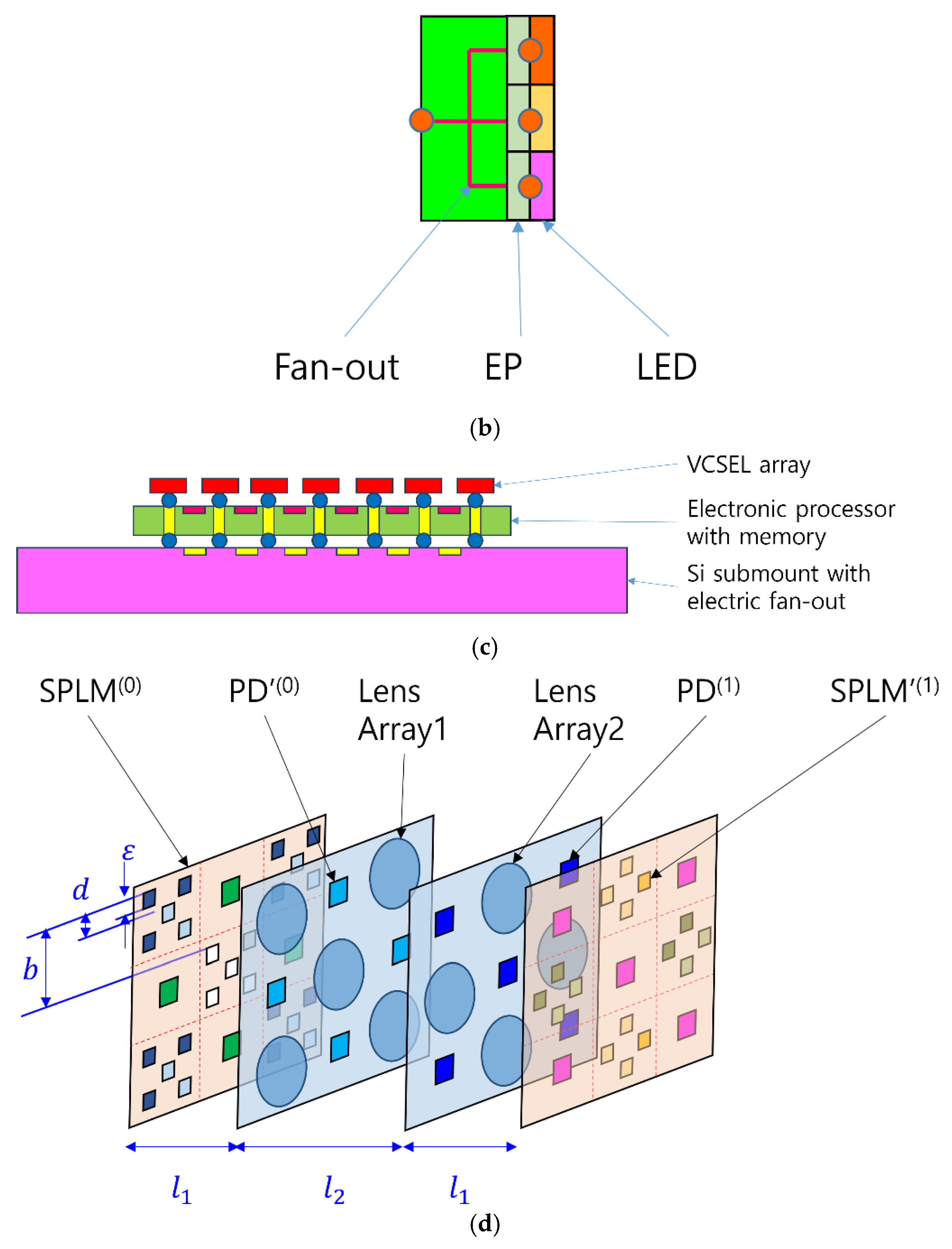
When the Sym-SPBOCNN is cascaded into a multi-layer configuration, each substrate must include an SPLM array on both sides to support forward and backward data flow, as illustrated in
Figure 4. In
Figure 3(a), the zeroth substrate has a detector on the left because it is assumed that the input is provided by the image relayed from the preceding optical stage.
4. Discussion
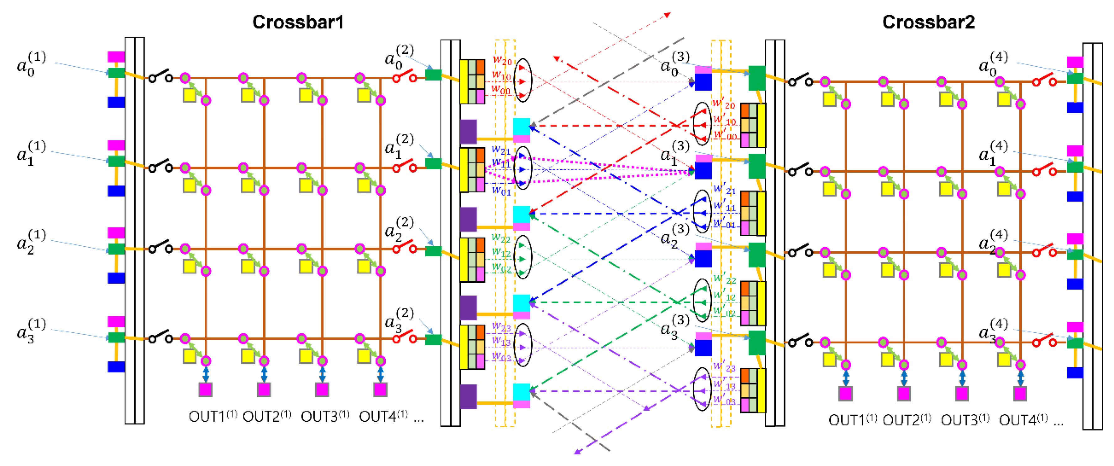
The Sym-SPBOCNN can be integrated with crossbar switches, as described in [
26], to implement a two-mirror-like architecture with data rearrangement between layers, as shown in
Figure 5. The bidirectional nature of Sym-SPBOCNN can emulate the arbitrary multiple layers using only two physical layers by bouncing the data between the two layers using memory of SPLM and its high-speed refresh rate. The crossbar switches enable permutation of the data set, allowing the data format to be reconfigured between layers and providing greater algorithmic flexibility in neural-network computation, as explained in detail in the previous report [
25]. Since the Sym-SPBOCNN inherit the much properties of SPBOCNN except that it simplifies the optical structures by using a unified optical arrangement for both directions, it also can take advantage of the TML-SPBOCNN with crossbar switches.
Another advantage of the Sym-SPBOCNN is its optical simplicity, as the detailed optical designs have already been demonstrated in earlier studies [
27]. Unlike architectures that require diffraction elements to split beams for backward propagation, the Sym-SPBOCNN does not demand such complex optical components. Systems that rely on different optical configurations for backward propagation require additional fabrication steps and precise optical alignment, which increases manufacturing, assembly, and maintenance costs. In contrast, the symmetric design of the Sym-SPBOCNN significantly reduces these burdens, offering improved cost efficiency and enhanced system reliability.
5. Conclusions
This work presented a theoretical framework for a Sym-SPBOCNN. By introducing geometric symmetry into the bidirectional free-space architecture, the proposed system allows forward and backward optical propagation to share identical lens arrangements, imaging distances, and pixel-level configurations. This unified design eliminates the asymmetry that previously required separate optical configurations, thereby simplifying alignment, reducing fabrication complexity, and improving overall system stability. The symmetry also ensures that the forward and backward channels exhibit identical optical characteristics, enabling consistent behavior during inference.
The analysis demonstrated that the Sym-SPBOCNN maintains the fundamental advantages of SPBOCNNs, including ultrafast reconfigurability enabled by SPLMs with integrated EP memory. The SPLM architecture supports nanosecond-scale weight updates and high-bandwidth modulation, allowing real-time kernel refresh rates suitable for multilayer CNN processing. Moreover, the interlaced placement of SPLMs and photodetectors allows for a compact bidirectional layout while reducing the number of optical components needed for backward propagation. This architectural simplification significantly lowers cost and manufacturing barriers relative to earlier bidirectional SPBOCNN designs.
Scalability analysis showed that the Sym-SPBOCNN can practically support kernel sizes up to 46×46 under typical lens-array constraints, which is sufficient for a broad range of CNN operations. Although this kernel size is smaller than the theoretical limit of SOCNN architectures, the reduction stems from the interlaced bidirectional pixel arrangement. Nevertheless, the proposed architecture remains fully compatible with clustering and software-based scaling methods, allowing flexible expansion to substantially larger computational workloads.
Performance estimates indicate that the Sym-SPBOCNN is capable of extremely high throughput, exceeding 4.1×10¹⁴ MAC/s with a single layer of 4K-resolution SPLMs and surpassing 4.1×10¹⁵ MAC/s when ten layers operate in a pipelined configuration. Because kernel updates can be executed concurrently with ongoing optoelectronic processing, these throughput figures can be sustained without additional delay, making the architecture well suited for real-time optical AI workloads.
Overall, the Sym-SPBOCNN provides a simplified yet powerful bidirectional optical computing framework that bridges optical parallelism with electronic adaptability. Its compatibility with CMOS backplanes, VCSEL arrays, and 3-D packaging methodologies suggests strong potential for future hardware realization. Continued research will focus on experimental prototyping, integration with crossbar-based reconfiguration networks, and joint algorithm–hardware co-optimization to fully exploit the capabilities of symmetrical optical neural processors.
Funding
This research received no external funding
Data Availability Statement
The datasets generated during and/or analyzed during the current study are available from the corresponding author on reasonable request.
Acknowledgments
In this section, you can acknowledge any support given which is not covered by the author contribution or funding sections. This may include administrative and technical support, or donations in kind (e.g., materials used for experiments).
Conflicts of Interest
The authors declare no conflicts of interest.
Abbreviations
The following abbreviations are used in this manuscript:
| CNN |
Convolutional neural network |
| OCNN |
Optical convolutional neural network |
| SLM |
Spatial light modulator |
| SOCNN |
Scalable Optical CNN |
| SPOCNN |
Smart-pixel-based optical convolutional neural network |
| SPLM |
Smart pixel light modulator |
| EP |
Electronic processor |
| LED |
Light-emitting diode |
| SPBOCNN |
Smart-pixel-based bidirectional optical convolutional neural network |
| Sym-SPBOCNN |
Symmetrical Smart-Pixel-Based Bidirectional Optical CNN |
| LCOE |
Linear combination optical engine |
| LD |
Laser diode |
| PD |
Photo diode |
| TML-SPBOCNN |
Two-mirror-like SPBOCNN |
| VCSEL |
Vertical-cavity surface-emitting laser |
| MAC |
Multiply-And-Accumulate |
| SPONN |
Smart-pixel-based optical neural network |
References
- Hinton, G.; Deng, L.; Yu, D.; Dahl, G.E.; Mohamed, A.R.; Jaitly, N.; Senior, A.; Vanhoucke, V.; Nguyen, P.; Sainath, T.N.; Kingsbury, B. Deep neural networks for acoustic modeling in speech recognition: The shared views of four research groups. IEEE Signal processing magazine 2012, 29, 82–97. [Google Scholar] [CrossRef]
- LeCun, Y.; Bengio, Y.; Hinton, G. Deep learning. Nature 2015, 521, 436–444. [Google Scholar] [CrossRef] [PubMed]
- Lecun, L.; Bottou, L.; Bengio, Y.; Haffner, P. Gradient-based learning applied to document recognition. Proceedings of the IEEE 1998, 86 2278–2324. [Google Scholar] [CrossRef]
- Rhu, M.; Gimelshein, N.; Clemons, J.; Zulfiqar, A.; Keckler, S.W. vDNN: Virtualized deep neural networks for scalable, memory-efficient neural network design. 2016 49th Annual IEEE/ACM International Symposium on Microarchitecture (MICRO), 2016; pp. 1–13. [Google Scholar]
- Chen, T.; Moreau, T.; Jiang, Z.; Zheng, L.; Yan, E.; Shen, H.; Cowan, M.; Wang, L.; Hu, Y.; Ceze, L.; Guestrin, C. TVM: An automated end-to-end optimizing compiler for deep learning. 13th USENIX Symposium on Operating Systems Design and Implementation (OSDI 18), 2018; pp. 578–594. [Google Scholar]
- Sze, V.; Chen, Y.-H.; Yang, T.-J.; Emer, J.S. Efficient Processing of Deep Neural Networks: A Tutorial and Survey. Proc. IEEE 2017, 2017(105), 2295–2329. [Google Scholar] [CrossRef]
- Han, S.; Pool, J.; Tran, J.; Dally, W. Learning both weights and connections for efficient neural network. Advances in Neural Information Processing Systems 2015, 28. [Google Scholar]
- Jouppi, N.P.; Young, C.; Patil, N.; Patterson, D.; Agrawal, G.; Bajwa, R.; Bates, S.; Bhatia, S.; Boden, N.; Borchers, A.; Boyle, R. In-datacenter performance analysis of a tensor processing unit. In Proceedings of the 44th Annual International Symposium on Computer Architecture, 2017; pp. 1–12. [Google Scholar]
- Colburn, S.; Chu, Y.; Shilzerman, E.; Majumdar, A. Optical frontend for a convolutional neural network. Applied optics 2019, 58, 3179–3186. [Google Scholar] [CrossRef] [PubMed]
- Chang, J.; Sitzmann, V.; Dun, X.; Heidrich, W.; Wetzstein, G. Hybrid optical-electronic convolutional neural networks with optimized diffractive optics for image classification. Scientific reports 2018, 8, 12324. [Google Scholar] [CrossRef] [PubMed]
- Lin, X.; Rivenson, Y.; Yardimci, N.T.; Veli, M.; Luo, Y.; Jarrahi, M.; Ozcan, A. All-optical machine learning using diffractive deep neural networks. Science 2018, 361, 1004–1008. [Google Scholar] [CrossRef] [PubMed]
- Sui, X.; Wu, Q.; Liu, J.; Chen, Q.; Gu, G. A review of optical neural networks. IEEE Access 2020, 8, 70773–70783. [Google Scholar] [CrossRef]
- Goodman, J.W. Introduction to Fourier optics; Roberts and Company publishers, 2005. [Google Scholar]
- Cox, M.A.; Cheng, L.; Forbes, A. Digital micro-mirror devices for laser beam shaping. Proc. SPIE 11043, Fifth Conference on Sensors, MEMS, and Electro-Optic Systems, 2019; p. 110430Y. [Google Scholar]
- Mihara, K.; Hanatani, K.; Ishida, T.; Komaki, K.; Takayama, R. High Driving Frequency (> 54 kHz) and Wide Scanning An-gle (> 100 Degrees) MEMS Mirror Applying Secondary Resonance For 2K Resolution AR/MR Glasses. 2022 IEEE 35th Inter-national Conference on Micro Electro Mechanical Systems Conference (MEMS), 2022; pp. 477–482. [Google Scholar]
- Glaser, I. Lenslet array processors. Applied Optics 1982, 21, 1271–1280. [Google Scholar] [CrossRef] [PubMed]
- Arecchi, A.V.; Messadi, T.; Koshel, R.J. Field Guide to Illumination. In SPIE Field Guides vol FG11; SPIE Press: Bellingham, 2007; p. 59. [Google Scholar]
- Greivenkamp, J.E. Field Guide to Geometrical Optics (SPIE Field Guides Vol. FG01), p.58; SPIE press: Bellingham, 2004; p. 28, 73. [Google Scholar]
- Ju, Y.G. Scalable Optical Convolutional Neural Networks Based on Free-Space Optics Using Lens Arrays and a Spatial Light Modulator. Journal of Imaging 2023, 9(11), 241. [Google Scholar] [CrossRef] [PubMed]
- Ju, Y.-G. A Conceptual Study of Rapidly Reconfigurable and Scalable Optical Convolutional Neural Networks Based on Free-Space Optics Using a Smart Pixel Light Modulator. Computers 2025, 14, 111. [Google Scholar] [CrossRef]
- Seitz, P. Smart Pixels. PROCEEDINGS EDMO 2001 / VIENNA 2001, 229–234. [Google Scholar]
- Hinton, H.S. Progress in the smart pixel technologies. IEEE journal of selected topics in quantum electronics 1996, 2(1), 14–23. [Google Scholar] [CrossRef]
- Ju, Y.G. A scalable optical computer based on free-space optics using lens arrays and a spatial light modulator. Optical and Quantum Electronics 2023, 55, 1–21. [Google Scholar] [CrossRef]
- James Singh, K.; Huang, Y.M.; Ahmed, T.; Liu, A.C.; Huang Chen, S.W.; Liou, F.J.; Wu, T.; Lin, C.C.; Chow, C.W.; Lin, G.R.; Kuo, H.C. Micro-LED as a promising candidate for high-speed visible light communication. Applied Sciences 2020, 10(20), 7384. [Google Scholar] [CrossRef]
- Feng, M.; Wu, C. -H.; Holonyak, N. Oxide-Confined VCSELs for High-Speed Optical Interconnects. IEEE Journal of Quantum Electronics 2018, 54(3), 1–15. [Google Scholar] [CrossRef]
- Ju, Y.-G. Reconfigurable Smart-Pixel-Based Optical Convolutional Neural Networks Using Crossbar Switches: A Conceptual Study. Electronics 2025, 14, 3219. [Google Scholar] [CrossRef]
- Ju, Y.-G. Optical Design of a Smart-Pixel-Based Optical Convolutional Neural Network. Optics 2025, 6, 19. [Google Scholar] [CrossRef]
|
Disclaimer/Publisher’s Note: The statements, opinions and data contained in all publications are solely those of the individual author(s) and contributor(s) and not of MDPI and/or the editor(s). MDPI and/or the editor(s) disclaim responsibility for any injury to people or property resulting from any ideas, methods, instructions or products referred to in the content. |
© 2025 by the authors. Licensee MDPI, Basel, Switzerland. This article is an open access article distributed under the terms and conditions of the Creative Commons Attribution (CC BY) license (http://creativecommons.org/licenses/by/4.0/).