Submitted:
09 December 2025
Posted:
18 December 2025
You are already at the latest version
Abstract
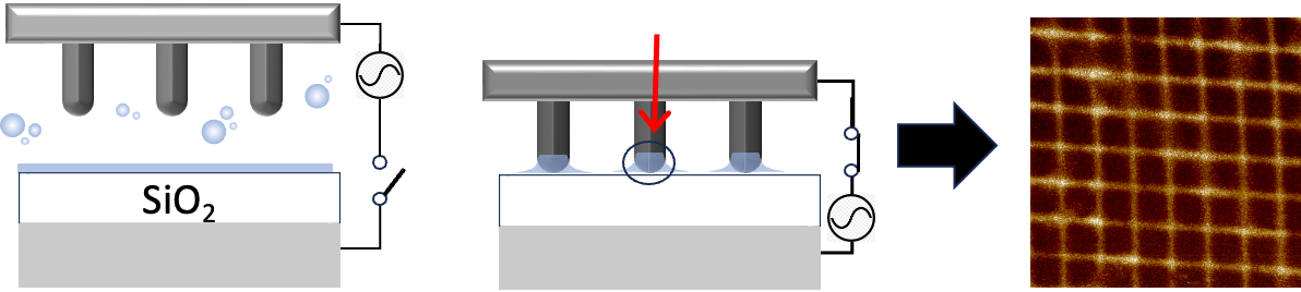
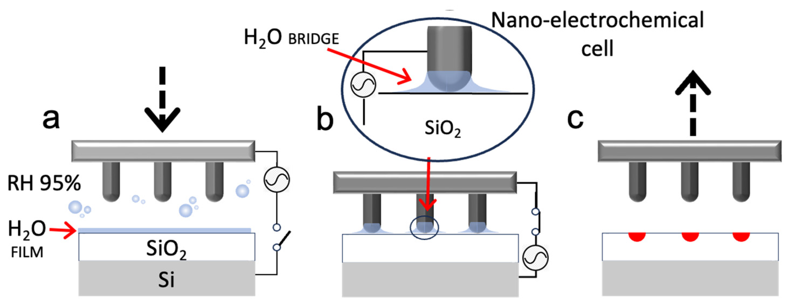
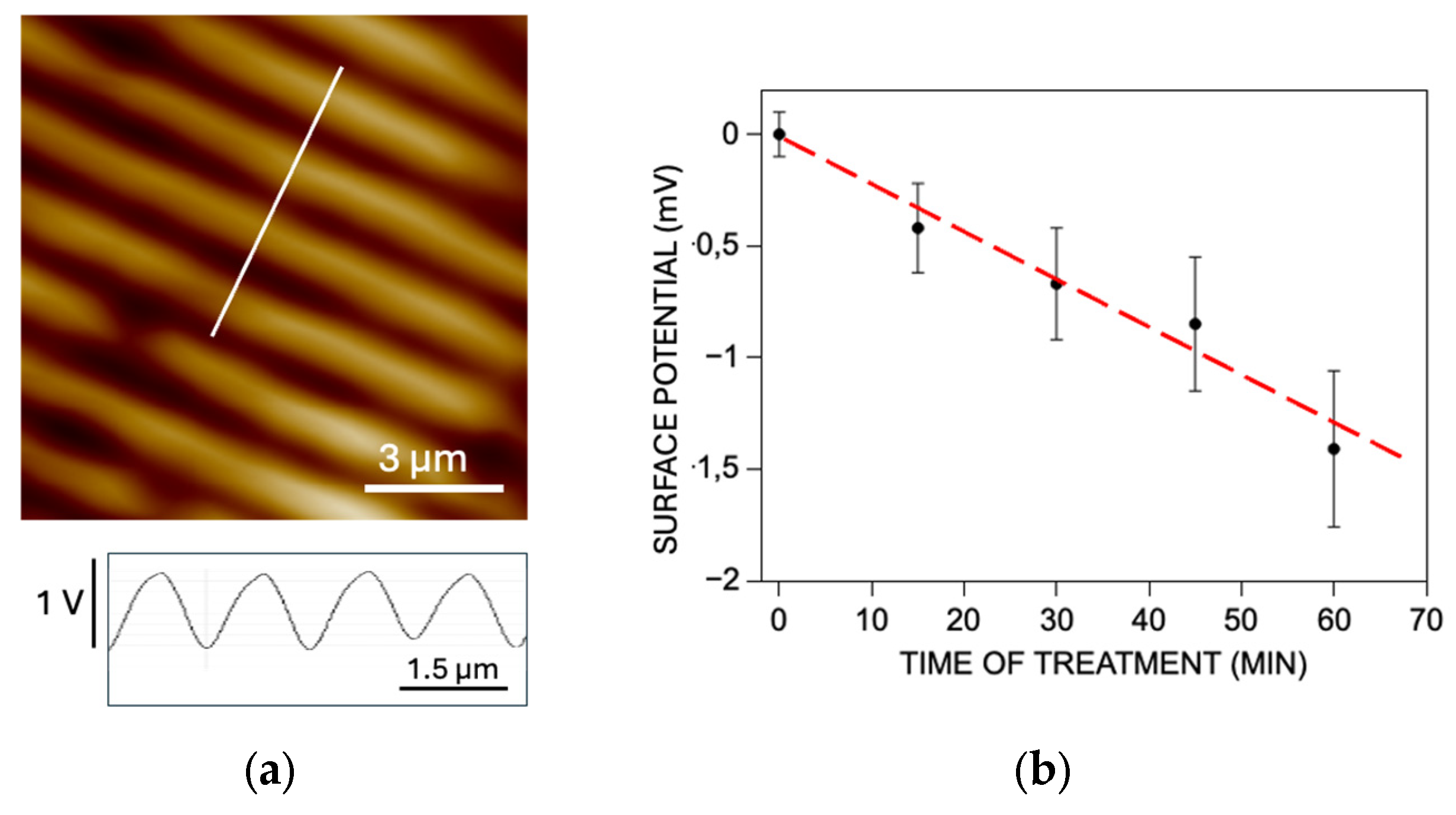
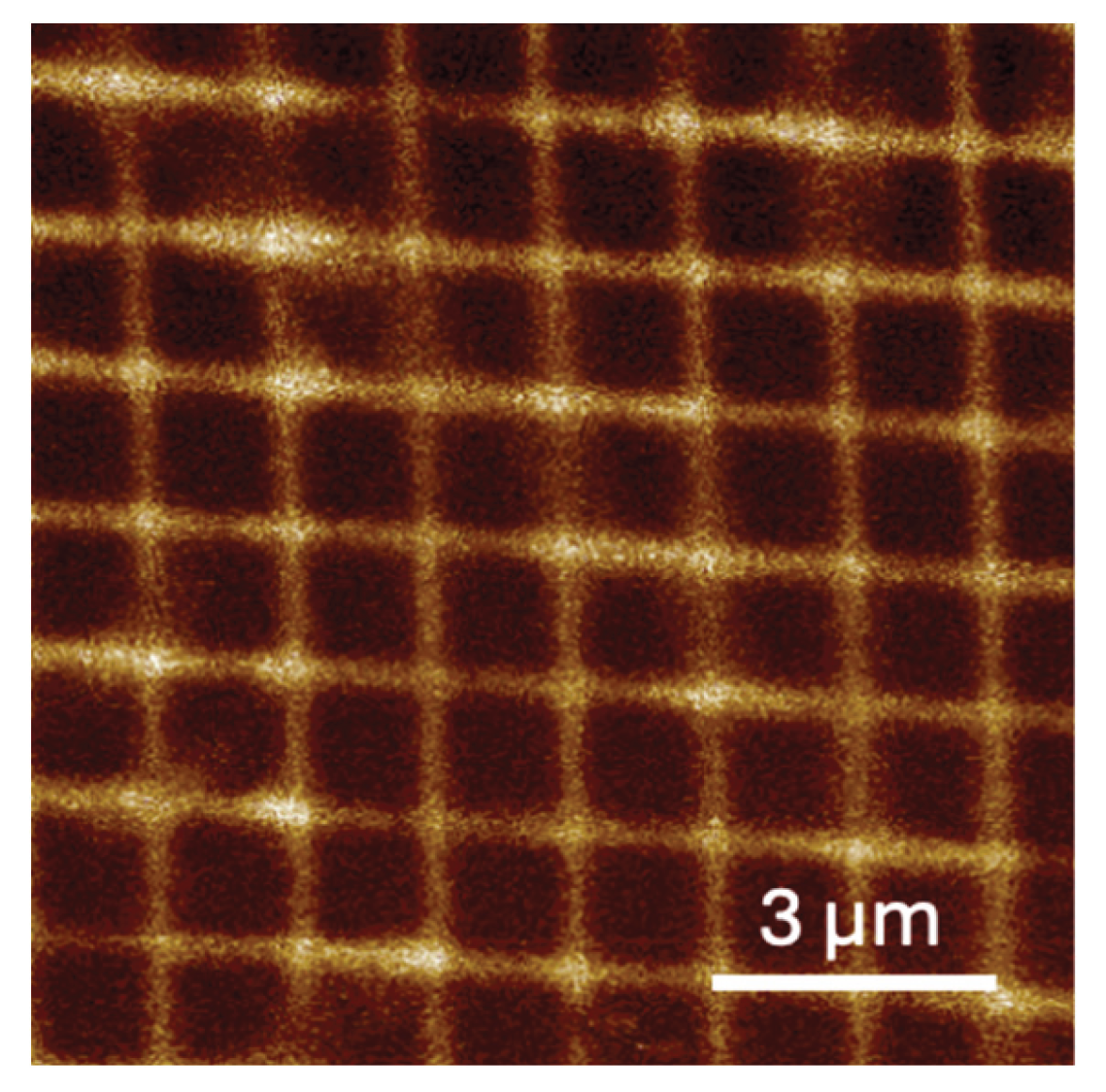
This work introduces a new method for creating patterned SiO₂ electrets using Electrode-Free Electrochemical Nanolithography (EFEN), enabling surface functionalisation without direct electrode contact. EFEN applies an alternating current through capacitive coupling between a conductive stamp and an insulating substrate in high-humidity conditions, forming a nano-electrochemical cell that drives localised reactions. Using thermally grown SiO₂ films, we achieve submicrometre patterning with minimal topographical impact but significant electronic alterations. Characterisation via Kelvin Probe Force Microscopy and Electric Force Microscopy confirms the formation of charged regions replicating the stamp pattern, with adjustable surface potential shifts up to –1.7 V and charge densities reaching 300 nC·cm⁻². The process can be scaled to areas of 1 cm² and is compatible with conventional laboratory equipment, offering a high-throughput alternative to scanning-probe lithography. EFEN combines simplicity, accuracy, and scalability, opening new opportunities for patterned electret production and functional surface engineering.
Keywords:
1. Introduction
2. Results and Discussion
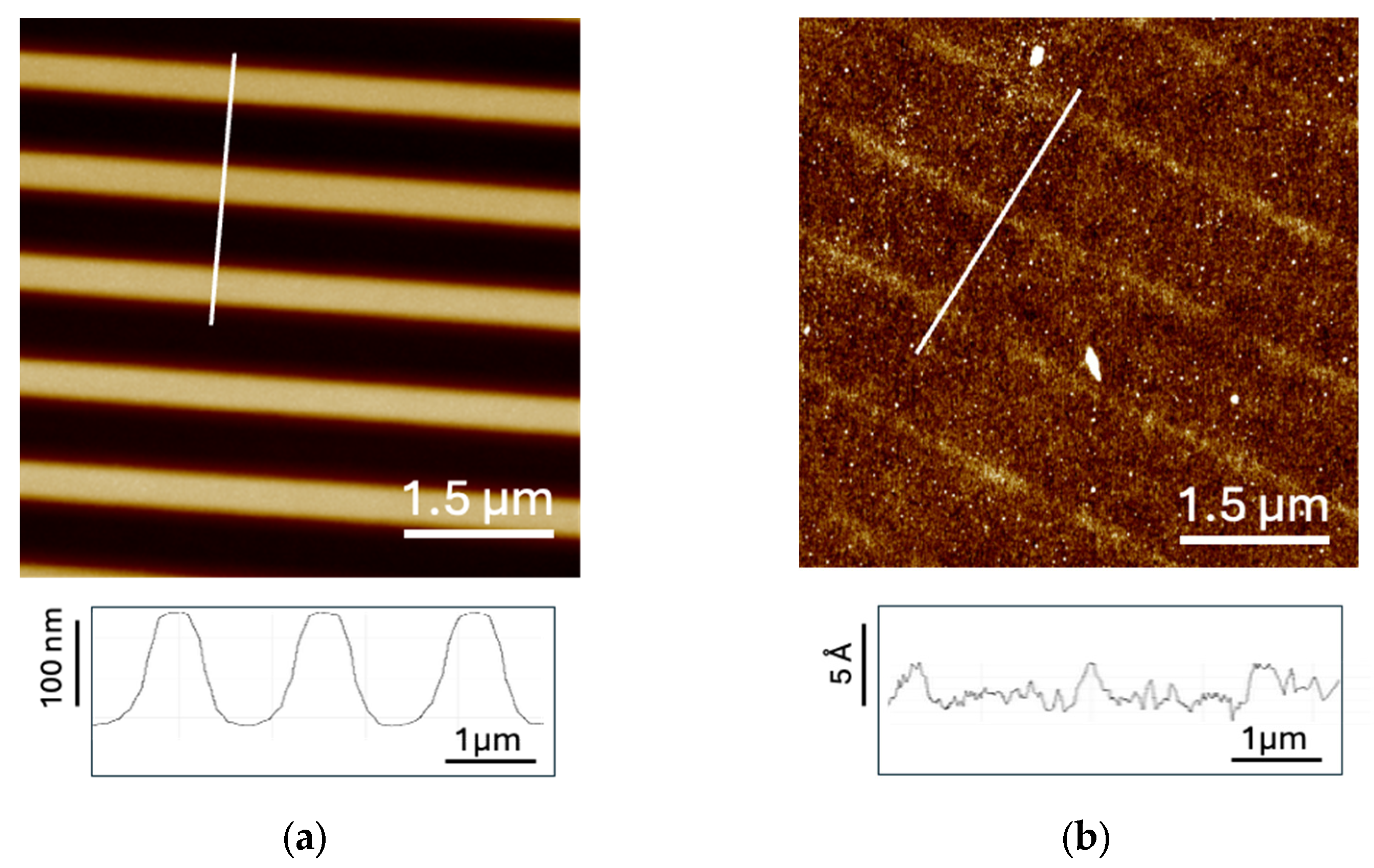
2.1. Method
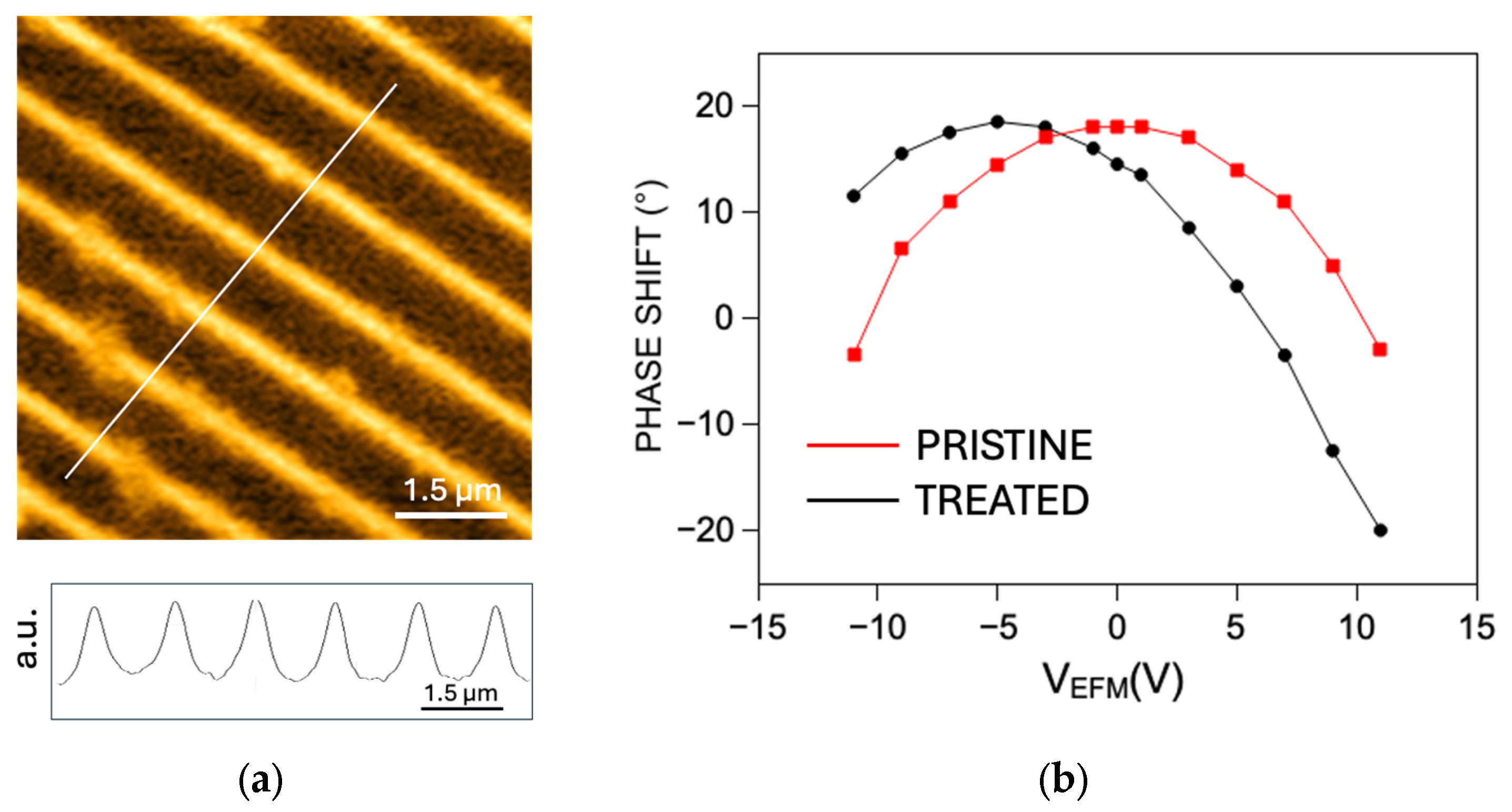
2.2. Electric Force Microscopy
2.2. Kelvin Probe Force Microscopy
4. Conclusions
Funding
Data Availability Statement
Conflicts of Interest
References
- Liang, F.; Li, H.Y.; Wang, Y.; Kuang, S.Y.; Fan, Y.J.; Wang, Z.L.; Zhu, G. Charge Distribution and Stability of SiO2 Nanoarray Electret. Chemnanomat 2020, 6, 212–217. [Google Scholar] [CrossRef]
- Ma, X.L.; Zhao, D.; Xue, M.Q.; Wang, H.; Cao, T.B. Selective Discharge of Electrostatic Charges on Electrets Using a Patterned Hydrogel Stamp. Angew Chem Int Edit 2010, 49, 5537–5540. [Google Scholar] [CrossRef] [PubMed]
- Zhang, Y.H.; Zhao, D.; Tan, X.X.; Cao, T.B.; Zhang, X. AFM Force Mapping for Characterizing Patterns of Electrostatic Charges on SiO2 Electrets. Langmuir 2010, 26, 11958–11962. [Google Scholar] [CrossRef] [PubMed]
- Melucci, M.; Zambianchi, M.; Favaretto, L.; Palermo, V.; Treossi, E.; Montalti, M.; Bonacchi, S.; Cavallini, M. Multicolor, large-area fluorescence sensing through oligothiophene-self-assembled monolayers. Chem. Commun. 2011, 47, 1689–1691. [Google Scholar] [CrossRef] [PubMed]
- Gentili, D.; Sonar, P.; Liscio, F.; Cramer, T.; Ferlauto, L.; Leonardi, F.; Milita, S.; Dodabalapur, A.; Cavallini, M. Logic-gate devices based on printed polymer semiconducting nanostripes. Nano Letters 2013, 13, 3643–3647. [Google Scholar] [CrossRef]
- Cavallini, M.; Hemmatian, Z.; Riminucci, A.; Prezioso, M.; Morandi, V.; Murgia, M. Regenerable Resistive Switching in Silicon Oxide Based Nanojunctions. Adv. Mater. 2012, 24, 1197–1201. [Google Scholar] [CrossRef]
- Leclere, P.; Surin, M.; Lazzaroni, R.; Kilbinger, A.F.M.; Henze, O.; Jonkheijm, P.; Biscarini, F.; Cavallini, M.; Feast, W.J.; Meijer, E.W.; et al. Surface-controlled self-assembly of chiral sexithiophenes. J. Mater. Chem. 2004, 14, 1959–1963. [Google Scholar] [CrossRef]
- Heaviside, O. Electromagnetic induction and its propagation. Electrization and electrification. Natural electrets. The Electrician 1885, 7, 230–231. [Google Scholar]
- Gerhard, R.; Ieee. Dielectric materials for electro-active (electret) and/or electro-passive (insulation) applications . 2nd International Conference on Electrical Materials and Power Equipment (ICEMPE), Guangzhou, China, 7–10 April 2019; pp. 91–96. [Google Scholar]
- Suzuki, Y. Recent progress in MEMS electret generator for energy harvesting. IEEJ Trans Electr Electron Eng 2011, 6, 101–111. [Google Scholar] [CrossRef]
- Kamogashira, T.; Yamasoba, T.; Kikuta, S.; Kondo, K. A Sleep Sensor Made with Electret Condenser Microphones. Clocks & Sleep 2025, 7, 28. [Google Scholar] [CrossRef]
- Jacobs, H.O.; Campbell, S.A.; Steward, M.G. Approaching nanoxerography: The use of electrostatic forces to position nanoparticles with 100 nm scale resolution. Adv Mater 2002, 14, 1553–1557. [Google Scholar] [CrossRef]
- Zimoch, L.; Schröder, S.; Elzenheimer, E.; Kaps, S.; Strunskus, T.; Faupel, F.; Höft, M.; Adelung, R. Electret integrated magnetic field sensor based on magnetostrictive polymer composite with nT resolution. Sci Rep 2025, 15, 1561. [Google Scholar] [CrossRef] [PubMed]
- Yasuda, T.; Komine, R.; Nojiri, R.; Takabe, Y.; Nara, K.; Kaneko, T.; Horigome, S.; Takeda, Y.; Wang, Y.-F.; Kawaguchi, S.; et al. Ultra-Rapidly Responsive Electret-Based Flexible Pressure Sensor via Functional Polymeric Nanoparticle Synthesis. Adv Fun Mater 2024, 34, 2402064. [Google Scholar] [CrossRef]
- Hu, L.; Li, X.; Guo, X.Y.; Xu, M.X.; Shi, Y.Q.; Herve, N.B.; Xiang, R.; Zhang, Q. Electret Modulation Strategy to Enhance the Photosensitivity Performance of Two-Dimensional Molybdenum Sulfide. Acs Appl Mater Inter 2023, 15, 59704–59713. [Google Scholar] [CrossRef]
- Xu, S.; Guan, X.; Bian, K.; Zhu, Q.; Dai, N.; Zhao, X.; Qiu, Y.; Zheng, S.; Dong, Y.; Zhong, J.; et al. Electret actuators enabling dual functions of optical ranging and audio feedback to elevate non-contact human-machine interactions. Nano Energy 2024, 125, 109553. [Google Scholar] [CrossRef]
- Mescheder, U.; Müller, B.; Baborie, S.; Urbanovic, P. Properties of SiO2 electret films charged by ion implantation for MEMS-based energy harvesting systems. J Micromech Microeng 2009, 19, 094003. [Google Scholar] [CrossRef]
- Guo, Z.F.; Patil, Y.; Shinohara, A.; Nagura, K.; Yoshida, M.; Nakanishi, T. Organic molecular and polymeric electrets toward soft electronics. Mol Syst Des Eng 2022, 7, 537–552. [Google Scholar] [CrossRef]
- Bonilla, R.S.; Wilshaw, P.R. Potassium ions in SiO2: Electrets for silicon surface passivation. J Phys D: Appl Phys 2017, 51, 025101. [Google Scholar] [CrossRef]
- Minami, T.; Utsubo, T.; Yamatani, T.; Miyata, T.; Ohbayashi, Y. SiO2 electret thin films prepared by various deposition methods. Thin Solid Films 2003, 426, 47–52. [Google Scholar] [CrossRef]
- Juberi, A.M.; Saha, P.C.; Faruqe, O.; Park, C. Partial Discharge Characteristics of SiO₂/Si₃N₄ Electret Incorporated AlN Substrates. IEEE T Transp Electr 2024, 10, 7796–7803. [Google Scholar] [CrossRef]
- Kim, Y.J.; Yang, C.H. Electret formation in transition metal oxides by electrochemical amorphization. Npg Asia Mater 2020, 12, 1. [Google Scholar] [CrossRef]
- Zahmatkeshsaredorahi, A.; Millan-Solsona, R.; Jakob, D.S.; Collins, L.; Xu, X.G. Kelvin probe force microscopy under ambient conditions. Nat Revi. Methods Primers 2025, 5, 53. [Google Scholar] [CrossRef]
- Albonetti, C.; Chiodini, S.; Annibale, P.; Stoliar, P.; Martinez, R.V.; Garcia, R.; Biscarini, F. Quantitative phase-mode electrostatic force microscopy on silicon oxide nanostructures. J Microscopy 2020, 280, 252–269. [Google Scholar] [CrossRef]
- Li, H.Y.; Ying, Z.; Lyu, B.S.; Deng, A.L.; Wang, L.L.; Taniguchi, T.; Watanabe, K.; Shi, Z.W. Electrode-Free Anodic Oxidation Nanolithography of Low-Dimensional Materials. Nano Lett 2018, 18, 8011–8015. [Google Scholar] [CrossRef]
- Gentili, D.; Calabrese, G.; Lunedei, E.; Borgatti, F.; Mirshokraee, S.A.; Benekou, V.; Tseberlidis, G.; Mezzi, A.; Liscio, F.; Candini, A.; et al. Tuning Electronic and Functional Properties in Defected MoS2 Films by Surface Patterning of Sulphur Atomic Vacancies. Small Methods 2025, 9, 2401486. [Google Scholar] [CrossRef]
- Gentili, D.; Chini, E.; Cavallini, M. Generation and Tuning of Semiconductor Electronic and Functional Properties through Electrochemical Patterning. Acc. Mater. Res. 2025, 6, 1094–1104. [Google Scholar] [CrossRef]
- Qi, G.C.; Yan, H.; Guan, L.; Yang, Y.L.; Qiu, X.H.; Wang, C.; Li, Y.B.; Jiang, Y.P. Characteristic capacitance in an electric force microscope determined by using sample surface bias effect. J App Phys 2008, 103, 114311-1. [Google Scholar] [CrossRef]
Disclaimer/Publisher’s Note: The statements, opinions and data contained in all publications are solely those of the individual author(s) and contributor(s) and not of MDPI and/or the editor(s). MDPI and/or the editor(s) disclaim responsibility for any injury to people or property resulting from any ideas, methods, instructions or products referred to in the content. |
© 2025 by the authors. Licensee MDPI, Basel, Switzerland. This article is an open access article distributed under the terms and conditions of the Creative Commons Attribution (CC BY) license (https://creativecommons.org/licenses/by/4.0/).


