
Submitted:
16 December 2025
Posted:
18 December 2025
You are already at the latest version
Abstract
This work presents a time-domain analog-to-digital conversion method in which the amplitude of a sensor signal is encoded through its crossing instants with a periodic ramp. The proposed architecture departs from conventional ADC and PWM demodulation approaches by shifting quantization entirely to the time domain, enabling waveform reconstruction using only a ramp generator, an analog comparator, and a timer capture module. A theoretical framework is developed to formalize the voltage-to-time mapping, derive expressions for resolution and error, and identify conditions that ensure monotonicity and single-crossing behavior. Simulation results demonstrate high-fidelity reconstruction for both periodic and non-periodic signals, including real photoplethysmographic (PPG) waveforms, with errors approaching the theoretical quantization limit. A hardware implementation on a PSoC 5LP microcontroller confirms the practicality of the method under realistic operating conditions. Despite ramp nonlinearity, comparator delay, and sensor noise, the system achieves effective resolutions above 12 bits using only native mixed-signal peripherals and no conventional ADC. These results show that accurate waveform reconstruction can be obtained from purely temporal information, positioning time-encoded sensing as a viable alternative to traditional amplitude-based conversion. The minimal analog front end, low power consumption, and scalability of timer-based processing highlight the potential of the proposed approach for embedded instrumentation, distributed sensor nodes, and biomedical monitoring applications.
Keywords:
time-based signal processing
; analog-to-time conversion
; ramp crossing
; timer capture
; sensor interface
; embedded instrumentation
1. Introduction
Sensor-enabled systems are essential in modern embedded applications, including environmental monitoring, industrial automation, wearable electronics, smart infrastructures, and Internet-of-Things (IoT) devices. In these fields, sensors usually generate analog signals that must be digitized before processing, interpretation, or transmission. This makes analog-to-digital conversion a key operation in embedded instrumentation and sensor interfaces. Traditional ADC architectures perform quantization in the voltage domain and require comparators, sample-and-hold circuits, reference generators, and other analog front-end components [1]. Although effective, these circuits increase size, power consumption, and design complexity factors critical in low-cost, compact, or energy-limited platforms such as IoT nodes and Industry 4.0 systems [2,3]. Alternatively, time-based signal-processing techniques leverage the high temporal resolution of digital timers and counters to encode analog signals as time intervals. This analog-to-time conversion approach has demonstrated that digital systems can attain competitive resolution with minimal analog circuitry, providing a promising solution for simplified sensor interfaces in modern embedded systems.
Direct interface circuits (DICs) have become a cost-effective, low-power solution for sensor acquisition in embedded systems. Review studies in the field have highlighted the increasing importance of these quasi-digital sensor interfaces, showing their effectiveness with resistive, capacitive, and inductive transducers across different application areas [4,5]. In these methods, the sensor connects directly to a microcontroller or FPGA's digital port without the need for a traditional ADC. By leveraging the natural Schmitt-trigger behavior of digital input pins, DICs offer reliable threshold detection and minimize switching noise. As a result, many passive sensors can be measured with only a few passive components, greatly reducing hardware complexity, size, and power consumption—especially advantageous in battery-powered and IoT sensor nodes.
Several ADC-less acquisition methods have been introduced in the literature to connect analog voltage sensors directly to microcontrollers and FPGAs. To provide context for these contributions, Table 1 summarizes the main features, hardware requirements, and limitations of key ADC-less approaches. Early research showed that microcontrollers without internal ADCs could mimic first-order delta–sigma converters using their analog comparators and a simple RC network. Peter et al. [6] demonstrated that a PIC16 device could perform ΔΣ conversion entirely in firmware, requiring only a few passive components. Subsequent developments improved resolution and robustness: Soldera et al. [7] developed a continuous-time ΔΣ scheme for HC9S08Rx devices. At the same time, Weber and Windish [8] integrated an external AD7400 modulator with an MSP430 for industrial-grade interfaces. Delta–sigma approaches were also implemented in programmable logic. An influential design used the LVDS input buffer of an Altera Cyclone-IV FPGA as a high-speed comparator, enabling a fully digital ΔΣ converter with about 60 dB SNR and sampling rates up to 500 kS/s [9]. Although these methods are effective, they depend on oversampling, digital filtering, and careful parametric tuning.
An alternative research approach removes the comparator by leveraging the Schmitt trigger behavior of digital input pins. Bengtsson [10] demonstrated that analog voltages could be digitized using only two GPIO pins and an RC network, achieving an equivalent 12-bit resolution. However, this method has a highly nonlinear transfer characteristic, low bandwidth (≈ 65 Hz), and significant memory overhead due to the needed LUT for linearization. More recently, Grossi [11] introduced a duty-cycle-based astable multivibrator that enhances linearity, bypasses the initial capacitor pre-charge phase, and reduces LUT usage, providing better sampling efficiency at moderate rates.
Time-encoded processing has also been used in a different context. Reverter et al. [12] proposed a timer-based AM demodulator that relies on the crossing points between a periodic triangular ramp and the AM signal. Although this design was meant for envelope extraction rather than arbitrary waveform digitization, it established a key principle: analog amplitude can be converted into timing information through controlled ramp-crossing events.
The present work differs from Reverter’s approach in two main aspects. First, instead of recovering the envelope of an amplitude-modulated signal, the proposed method uses ramp-crossing instants to digitize arbitrary analog sensor outputs. Second, it replaces the triangular ramp with a unidirectional sawtooth waveform, whose constant slope and single crossing per period establish a straightforward and monotonic relationship between signal amplitude and crossing time. This choice simplifies timing extraction, avoids ambiguity, improves linearity, and increases sampling efficiency. As a result, while Reverter’s method is suited for AM envelope detection, the sawtooth-based scheme presented here operates as a general-purpose analog-to-time converter capable of digitizing full waveforms without a conventional ADC.
This work introduces a sensor digitization method that does not rely on a conventional ADC but instead encodes analog amplitude in the time domain through ramp-crossing events. The objective is to demonstrate that sensor data can be accurately acquired and reconstructed using only standard microcontroller peripherals, thereby enabling a lightweight, fully time-based signal-acquisition strategy.
The main contributions of this paper are as follows:
- A time-domain analog-to-digital conversion method that replaces conventional amplitude quantization with ramp-crossing timing, enabling accurate waveform reconstruction using only comparator transitions and timer captures, and thereby eliminating the need for dedicated ADC hardware.
- An analytical framework and architectural formulation that characterize the voltage–time mapping, derive closed-form expressions for resolution and timing uncertainty, and establish the operating conditions required for monotonic and single-crossing behavior in practical mixed-signal implementations.
- Comprehensive validation through simulation and hardware experimentation, demonstrating high-fidelity reconstruction of sinusoidal and physiological PPG signals with effective resolutions above 12 bits, and confirming the practicality, efficiency, and scalability of time-based sensing for embedded and resource-constrained instrumentation.
Overall, the proposed method provides a compact, energy-efficient, and cost-effective alternative for smart sensor interfaces, offering a simple and scalable pathway to integrate analog sensing with digital processing in modern embedded systems.
2. System Architecture and Method
The proposed method performs the digitization of analog sensor signals by converting voltage into time information through periodic ramp crossings. Unlike conventional ADC-based conversion, where amplitude is directly quantized into discrete voltage levels, the proposed approach encodes the instantaneous amplitude of a sensor signal in the crossing time between the sensor voltage and a locally generated ramp. This time interval can be directly measured by a digital timer, providing an efficient analog-to-time conversion mechanism with minimal hardware requirements.
2.1. System Architecture
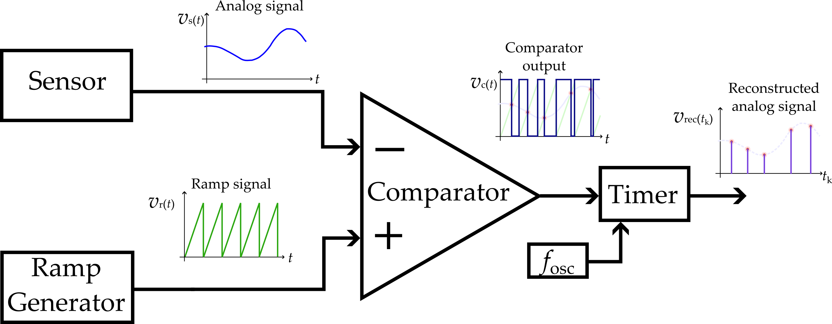
The overall structure of the proposed interface is shown conceptually in Figure 1. The system consists of three functional elements: the analog sensor, which provides the input signal vs(t); the ramp generator, which produces a linear sawtooth waveform vr(t) synchronized with the system timer; and the comparator–timer subsystem, which detects the exact instant at which the sensor signal intersects the ramp and records the elapsed time from the beginning of each ramp cycle. Together, these components enable a direct mapping from analog amplitude to time-domain information, forming the basis of the proposed analog-to-time conversion method. During each ramp period, Tr, the timer, measures the interval from the start of the ramp to the point where vs(t) equals vr(t). This estimated time indicates the instantaneous amplitude of the sensor signal. The digital processing stage converts the timing value to voltage using vs = VCC × tk / Tr and reconstructs the waveform by concatenating successive samples.
2.2. Timing Behavior
The time-domain operation of the method is shown in Figure 2. In the top plot, the sensor signal vs(t) (blue) is compared with a periodic ramp vr(t) (green). Each intersection (red dots) marks a valid crossing instant tk. The comparator output (middle trace) toggles at each crossing, producing a sequence of pulses whose timing encodes the signal amplitude. Finally, the bottom plot shows the reconstructed voltage vrec(tk), obtained from the captured crossing instants, which accurately follows the original waveform.
2.3. Implementation Guidelines
The proposed architecture can be easily implemented using standard mixed-signal microcontrollers equipped with analog comparators, DACs (or PWM outputs), and capture/compare timers. A periodic ramp can be generated either internally via a DAC or externally by low-pass filtering a PWM signal. The comparator may be an on-chip component or a discrete device, depending on noise and speed requirements. Its output is directed to a timer capture input, where each transition automatically records the crossing time tk. Key design parameters include:
- Ramp period Tr, which defines the temporal sampling rate;
- Ramp slope VCC/ Tr, which sets the voltage-to-time sensitivity; and
- Timer frequency fosc, which determines time-quantization resolution.
Linearity is maintained as long as the sensor signal slope is smaller than the ramp slope, ensuring a single, monotonic crossing per cycle. These relationships are further developed analytically in Section 3.
Microcontroller families, such as PSoC 5LP, STM32, MSP430, or PIC24, integrate all these peripherals, enabling straightforward implementation without the need for ADCs. The firmware synchronizes the ramp and timer, computes vs according to Eq. (2), and reconstructs the waveform if necessary.
3. Theoretical Analysis
The proposed method enables the reconstruction of an analog signal from time-domain data obtained through periodic ramp crossings. It works opposite to a PWM demodulation process. Instead of deriving amplitude from width-modulated pulses, the instantaneous amplitude of the sensor signal is determined from the crossing points between the signal and a linearly increasing ramp. This section offers the analytical formulation of the conversion process, its resolution, and the primary sources of error and nonlinearity.
3.1. Crossing Condition and Voltage–Time Mapping
Let vs(t) be the analog sensor signal and vr(t) a locally generated periodic ramp that increases linearly from 0 to VCC during a ramp period Tr. The comparator output toggles whenever both signals coincide:
where tk represents the instant at which the k-th crossing occurs.
From (1), the analog voltage can be expressed in terms of the crossing time:
Equation (2) forms the foundation of the proposed analog-to-time conversion, where amplitude information is encoded as a time variable that a digital timer can measure.
During continuous operation, a sequence of crossings is detected at instants t1, t2, ..., tk, each occurring during a different ramp cycle. In this case, the reconstructed voltage waveform is obtained by applying the modulo operation to ensure that each event is referenced to its local ramp period.
where (tk mod Tr) represents the temporal position of each crossing within the current ramp cycle, allowing the mapping to be applied iteratively over successive periods. This operation enables reconstruction of the entire analog waveform from discrete-time-encoded samples captured by the timer. Equation (3) is therefore the discrete-time extension of the continuous mapping in (2), allowing waveform reconstruction from time-stamped crossing events.
3.2. Resolution and Linearity
The achievable resolution of the time-based conversion depends on the timer clock frequency (fosc) and the ramp period (Tr). The number of quantization levels N provided by the timer can be expressed as:
For example, using a 100 MHz timer and a 1 ms ramp, a theoretical resolution of approximately 16.6 bits can be achieved. In the same way, even a 16 MHz oscillator, such as the one integrated in the ATmega328 microcontroller used on the Arduino Nano, would provide about 14 bits under the same ramp duration. This illustrates that time-based encoding can deliver high nominal resolutions using only standard on-chip timers, without requiring high-end clock sources or dedicated ADCs.
On the other hand, the method maintains linearity as long as the ramp has a constant slope. Deviations from linearity occur when the ramp generator introduces curvature, such as from DAC nonlinearity or RC filtering of a PWM signal. The reconstructed signal stays proportional to the actual sensor voltage as long as only one intersection occurs per cycle.
This condition is satisfied if the slope of the ramp exceeds that of the input signal:
ensuring there is only one stable crossing per period and stopping multiple triggering events.
3.3. Error and Uncertainty
In practical implementations, the main sources of error are timer quantization, comparator jitter, and ramp instability. From the voltage–time relationship in (2), the instantaneous error due to timing uncertainty Δt can be written as:
Assuming these errors are statistically independent, the total RMS voltage error of the reconstructed signal can be approximated as:
where σt, σr, and σc correspond to the standard deviations of timer quantization, ramp nonlinearity, and comparator jitter, respectively.
To minimize Δv, the system can either increase fosc or average multiple ramp cycles. In practice, the latter is preferable in low-power embedded systems, where high oscillator frequencies may not be feasible.
3.4. Quantization and Effective Resolution
In time-based digitization, the smallest measurable voltage step, or Least Significant Bit (LSB), depends on the ramp slope and the timer period, and can be expressed as:
The quantization RMS error caused by timer granularity is
The total measured RMS reconstruction error combines both quantization and other nonidealities:
where represents contributions from jitter, ramp curvature, and threshold noise.
The equivalent effective number of bits (ENOB) can then be estimated as:
with VFS denoting the full-scale voltage range.
3.5. Small-Signal Approximation
For slowly varying sensor signals, vs(t) can be considered approximately constant within each ramp period. In this small-signal regime, the time-domain samples (tk mod Tr) correspond linearly to the instantaneous amplitude, and (3) provides an accurate reconstruction. The overall response of the conversion can thus be modeled as a sampled version of the analog signal with an effective sampling rate equal to the ramp frequency fr = 1/Tr.
3.6. Large-Signal and Dynamic Effects
When the sensor signal varies greatly within a single ramp cycle, the assumption of constant amplitude no longer applies. This can cause multiple crossings or timing distortions, leading to amplitude compression or duplication. These issues can be minimized by increasing the ramp slope (reducing Tr) or prefiltering the input.
For signals with strong dynamics, the deviation in the crossing instant tk can be modeled through a first-order Taylor expansion:
which yields a nonlinear correction term to (3). This distortion becomes significant when approaches the ramp slope VCC / Tr.
3.7. Temporal Sampling and Reconstruction
Each ramp cycle produces a one-time-coded sample of the analog signal. Therefore, the effective sampling frequency of the system is equal to the ramp frequency fr. If the signal under test contains components higher than fr /2, aliasing will occur in the reconstructed waveform.
In practical applications, the ramp frequency can be chosen to satisfy the Nyquist criterion relative to the sensor bandwidth, or oversampling can be employed, followed by digital filtering. For quasi-periodic signals, such as the 60 Hz mains waveform used in the experimental setup, the ramp frequency (1–5 kHz) ensures sufficient temporal resolution to reconstruct both waveform shape and amplitude variations accurately.
3.8. Discussion
The theoretical formulation in Sections 3.2–3.6 establishes a direct, quantitative link between the sensor voltage and the ramp-crossing time, allowing for continuous analog reconstruction. Equations (2)–(3) specify the core voltage-to-time relationship, while Equations (4)–(12) outline the constraints from timer quantization, ramp slope, and nonideal effects like jitter and curvature.
The analysis shows that the ENOB increases logarithmically with the product of fosc and Tr (the timer clock frequency and ramp period) and decreases proportionally with sources of temporal noise. Specifically, increasing either the timer frequency or the ramp duration improves resolution, whereas comparator jitter and ramp nonlinearity reduce it by introducing additional timing uncertainty.
4. Simulation and Experimental Validation
This section describes the steps used to verify the performance of the proposed time-based sensor digitization method through both numerical simulations and hardware testing. Both validation steps follow the operating principle outlined in Section 2, where an analog sensor signal is continuously compared with a periodic ramp, and the crossing points are encoded as timing events.
4.1. Simulation Setup
To verify the feasibility and accuracy of the proposed timer-based digitization method, a numerical simulation was performed in Python using the NumPy, SciPy, and Matplotlib libraries. The simulation environment replicates the entire signal chain, including the analog sensor signal, the periodic ramp, and the comparator output that generates ramp-crossing events.
Two different input signals were considered:
- A 60 Hz sinusoidal waveform representing a typical analog signal derived from mains-powered loads. This signal emulates the fundamental component of household or industrial AC power. It serves as a reference for applications such as measuring electrical energy consumption, monitoring load behavior, or assessing power quality parameters.
- A photoplethysmographic (PPG) signal is a low-frequency, non-sinusoidal biosignal that reflects pulsatile changes in blood volume within peripheral tissues. In this work, a real PPG waveform is used, extracted from the BIDMC PPG and Respiration dataset available on PhysioNet (Goldberger et al. [13]; PhysioNet BIDMC Dataset [14]), which provides clinical-grade recordings acquired at 125 Hz. This type of signal is widely employed in biomedical instrumentation for heart rate estimation, cardiovascular monitoring, and wearable sensing applications, making it an illustrative example of a slowly varying analog waveform suitable for evaluating time-based digitization methods.
In both simulations, a sawtooth ramp served as the reference signal, increasing linearly from 0 V to VCC = 5 V. For the 60 Hz sinusoidal case, a 1 kHz ramp period (Tr = 1 ms) was chosen to achieve a high oversampling ratio. For the PPG example, a slower 80 Hz (Tr = 12.5 ms) ramp was used to match the lower bandwidth of physiological signals while still maintaining adequate temporal resolution. In all cases, the system was simulated using a 16 MHz time base to replicate the timing accuracy of a typical microcontroller clock. The comparator behavior was modeled by evaluating whether vs(t) > vr(t), and crossing instants were detected using the np.diff() operation on the comparator output.
Each detected crossing time, tk, was then converted into a reconstructed voltage value using the linear mapping Equation (3). This operation enables reconstruction of the entire analog waveform from discrete time-encoded samples captured across multiple ramp periods. The reconstruction accuracy of the proposed timer-based digitization method was evaluated by calculating the RMS error between the reconstructed voltage, vrec(tk), and the corresponding reference signal, vs(tk), at each detected ramp-crossing instant, tk. The RMS error is defined as:
where nc is the total number of valid crossings within the observation window.
This metric quantifies the voltage deviation introduced by the analog-to-time conversion process and aggregates the effects of timing quantization, ramp nonlinearity, comparator noise, and other non-idealities intrinsic to practical implementations. As such, ERMS constitutes a comprehensive indicator of the overall accuracy and fidelity of the proposed time-based digitization method.
4.2. Experimental Setup
Experimental verification was conducted to assess the feasibility of the proposed time-based digitization method under real operating conditions. The setup was built using a PSoC 5LP microcontroller, which includes all necessary mixed-signal peripherals: an internal DAC for ramp generation, an analog comparator, and a timer/counter set in capture mode. This configuration enables direct measurement of ramp-crossing instants and mirrors the simulation framework described in Section 4.1.
To maintain consistency with the simulated scenarios, two ramp frequencies were used, depending on the input waveform. For the mains current experiment, the DAC generated a 0–4 V sawtooth ramp at 1.25 kHz, providing a high oversampling ratio suitable for 60 Hz signals. For the PPG experiment, the ramp frequency was reduced to 80 Hz to match the lower bandwidth of physiological waveforms while ensuring adequate temporal resolution.
Two experimental arrangements were prepared, as illustrated in Figure 3a,b and 4a,b:
- In the first experiment, the current waveform was obtained using a YHDC SCT-013-000 non-invasive current transformer (CT), a widely used sensor for AC mains monitoring. This device provides galvanic isolation, a nominal range of 0–100 A AC, and a 2000:1 transformation ratio. Its current-mode secondary output was converted into a measurable voltage using an external burden resistor mounted on the breadboard. The resulting signal, proportional to the mains current, was applied to the PSoC comparator input for ramp-crossing detection. Figure 3a shows the schematic of this configuration, illustrating the connection between the CT, the DAC ramp generator, the comparator, and the timer/capture subsystem. Figure 3b presents a photograph of the physical setup, including the PSoC 5LP board, the SCT-013-000 sensor clamped to the mains cable, and the resistive heater used as a four-level variable load, along with the measurement equipment used during testing. A laptop running the reconstruction software and a digital oscilloscope (Keysight DSOX2014A) used for waveform verification are also visible, illustrating the complete hardware environment employed during validation. An OLED display module connected via I²C was included to provide real-time visualization of the reconstructed waveform, although the detailed analysis was performed offline.
- In the second experiment, a commercial optical heart-rate monitor (Pulse Sensor from World Famous Electronics) was used to acquire PPG waveforms. This reflective optical module outputs an analog signal proportional to pulsatile blood-volume changes. Its output was routed directly to the PSoC comparator input, enabling the system to record event timings associated with the evolving amplitude of the PPG waveform. For this test, the DAC generated a 0–4 V sawtooth ramp at 80 Hz, matching the slow dynamics of physiological signals. Figure 4a illustrates the schematic of the PPG acquisition setup, showing the sensor interface, the ramp generator, and the timer/capture logic. Figure 4b shows a photograph of the hardware arrangement, including the PSoC board, oscilloscope probes used for visual verification, and the PPG sensor placed on the subject’s fingertip.
In both experiments, each comparator transition generated a hardware interrupt that latched the current timer value, producing a sequence of timestamps tk corresponding to the ramp-crossing instants. These timestamps were transmitted to a host computer for offline processing in Python using the reconstruction procedure described in Section 4.1, ensuring methodological consistency between simulation and experimental evaluation. In parallel with the proposed time-based method, the analog input signal in each experiment was also sampled using the internal 12-bit ADC of the PsoC 5LP. This provided a conventional voltage-reference measurement, enabling a direct comparison between the ADC waveform and the time-encoded reconstruction. Both datasets were aligned in time and analyzed together to compute the RMS error, allowing a quantitative assessment of the accuracy and fidelity of the proposed digitization technique.
Results and Discussion
This section presents the simulation and experimental results used to validate the proposed time-based digitization method, comparing the reconstructed waveforms with their reference signals and evaluating the reconstruction error and effective resolution of the approach.
5.1. Simulated Results
5.1.1. Sinusoidal Signal
Figure 5a shows the blue sinusoidal waveform corresponding to a 60 Hz analog sensor signal, while the green lines represent the 1 kHz ramp generated for comparison. Each intersection between the two signals, marked by red points, corresponds to a valid crossing instant (tk) where the comparator toggles, encoding the analog amplitude as a temporal event. Each ramp period thus yields one time-encoded sample of the sensor voltage.
In Figure 5b, the red dots represent the reconstructed signal obtained from the sequence of crossing instants, while the blue dashed line shows the original reference waveform. The near-perfect overlap between both signals confirms that the time-domain mapping preserves the amplitude and phase information of the original signal with high fidelity. This confirms the high linearity predicted by the theoretical model in Section 3.
Figure 5c shows the instantaneous reconstruction error (red line) relative to the reference signal, along with gray dashed lines indicating the ±RMS error bounds. The error remains within ± 0.2 Mv, representing a deviation of only 0.004 % of the 5 V full-scale signal. The extremely small error confirms that timer quantization and ramp slope introduce negligible distortion under the simulated conditions.
The quantitative analysis of the simulated sinusoidal signal provides further Insight Into the resolution and linearity of the proposed method. From Eq. (8), the voltage resolution or LSB is 0.3125 Mv, considering VCC = 5 V, fosc=16 MHz, and Tr = 1 ms. According to Eq. (9), the corresponding quantization RMS error is Eq,RMS = 0.090 Mv. Using Eq. (11), the effective number of bits (ENOB) derived from RMS reconstruction error of 0.20 Mv is approximately 12.9 bits, which is only one bit below the theoretical ceiling of 13.97 bits established by Eq. (4). The reconstructed waveform also exhibits excellent linearity, with a correlation coefficient of R2 = 0.99999 relative to the reference signal.
Furthermore, the condition of Eq. (5) is fully satisfied, since the maximum slope of the input signal remains well below the ramp slope 5 Mv/μs, ensuring a single, monotonic crossing per cycle and confirming the high linearity predicted by the theoretical model. Finally, using Eq. (6), the equivalent timing uncertainty associated with the RMS error is approximately 40 ns, well below the timer’s 62.5 ns quantization step. This indicates that the method operates near its theoretical quantization limit, with timing accuracy governed primarily by ramp linearity rather than by timer resolution.
The simulated results confirm this behavior, achieving an effective resolution of 12.9 bits and exhibiting strong linearity and very low distortion, thereby validating the accuracy of the theoretical model and the fidelity of the time-based conversion process.
5.1.2. PPG Signal
The real PPG signal used in this study was extracted from the BIDMC PPG and Respiration Dataset on PhysioNet. The selected 4-second segment corresponds to the plethysmographic (PLETH) channel sampled at 125 Hz. This segment exhibits a dominant frequency of approximately 1.1–1.3 Hz, consistent with the typical heart rate range observed in clinical recordings from this database. Its morphology includes the characteristic steep systolic upstroke, the broader diastolic decay, and the presence of a dicrotic notch, reflecting genuine hemodynamic variability [13,14].
For this experiment, the ramp frequency was set to 80 Hz. Given the dominant PPG frequency of about 1.2 Hz in the extracted dataset, this configuration provides roughly 66 ramp crossings per cardiac cycle. This oversampling ratio is sufficient to preserve the physiologically relevant features of the waveform and ensures accurate reconstruction of the real PPG morphology under the proposed time-encoding method.
Figure 6a shows the blue PPG waveform and the green 80 Hz ramp, with each intersection point (red markers) representing a valid crossing event detected by the simulated comparator. The varying density of red markers demonstrates the amplitude modulation of the PPG signal: larger amplitude regions result in later crossings, while smaller amplitude regions occur earlier within each ramp cycle.
In Figure 6b, the red dots represent the reconstructed waveform obtained from the time-coded samples, while the blue dashed line corresponds to the original reference signal. The substantial visual overlap between the two confirms that the proposed analog-to-time conversion accurately reproduces the shape and dynamics of the PPG waveform, including the fast systolic rise and slower diastolic decay. This result demonstrates the ability of the method to digitize physiological signals with high amplitude fidelity and negligible distortion.
Figure 6c shows the instantaneous reconstruction error (red line) and the ±RMS bounds (gray dashed lines). The RMS reconstruction error is 10 µV, which is 0.0002% of the 5 V full-scale range. This very low error indicates that the quantization and temporal encoding cause virtually no measurable distortion during the 5 s observation window.
Using Eq. (6), the equivalent timing uncertainty can be estimated as 25 ns, which is below one timer tick (62.5 ns), indicating sub-tick precision in the crossing detection process. The quantitative analysis of the PPG simulation provides further insight into the resolution and temporal accuracy of the proposed method. For the parameters considering VCC = 5 V, fosc=16 MHz, and Tr = 12.5 ms, the voltage resolution or LSB obtained from Eq. (8) is 25 μV.
According to Eq. (9), the corresponding quantization RMS error is 7.2 μV. Using Eq. (11), the ENOB calculated from the RMS reconstruction error of 10 μV is approximately 14.9 bits. This effective resolution exceeds the 13-bit theoretical limit achieved for the 1 ms ramp case, owing to the longer ramp period (12.5 ms), which increases temporal granularity and voltage resolution while maintaining a single, monotonic crossing per cycle. These results demonstrate that extending the ramp period is a straightforward and effective way to enhance resolution in time-based digitization systems without increasing clock frequency or hardware complexity.
5.2. Experimental Results
5.2.1. Sinusoidal Signal
Figure 7a shows the oscilloscope capture of the experiment, where the bottom trace corresponds to the 60 Hz sensor voltage derived from the current transformer, the middle trace shows the 1.25 kHz sawtooth ramp generated by the DAC, and the top trace displays the comparator output that toggles at each ramp–signal intersection. The clean and periodic transitions confirm the presence of a single monotonically increasing crossing per ramp cycle, satisfying the condition of Eq. (5) under real operating conditions.
Figure 7b compares the reconstructed sinusoidal signal obtained from the sequence of experimentally measured crossing instants (red dots) with the 12-bit ADC reference waveform (blue dashed line). As in the simulated case, the two signals exhibit strong visual agreement, with the reconstructed samples closely following the amplitude and phase of the reference sinusoid throughout the full cycle. This overlap confirms that the time-domain encoding mechanism is preserved under real hardware conditions and that the proposed architecture successfully extracts the analog information using only the comparator, ramp generator, and timer subsystem. The overall fidelity of the reconstruction indicates that the linear relationship between crossing time and signal amplitude remains valid in practice, despite nonidealities in the front-end circuitry.
Figure 7c shows the instantaneous reconstruction error relative to the ADC reference, together with the ±RMS bounds. The experimental RMS reconstruction error is 0.01355 V, corresponding to approximately 0.27 % of the 5 V full-scale range. When normalized to the actual voltage span of the PSoC ramp generator (approximately 0–4.08 V) the relative error increases slightly to 0.33 %, but remains within the same order of magnitude. This adjustment highlights that part of the discrepancy between simulation and experiment is attributable to the reduced full-scale amplitude of the hardware DAC, rather than to limitations of the time-encoding method itself. Overall, the measured error remains small for a mixed-signal microcontroller implementation and reflects the combined effects of DAC ramp nonlinearity, comparator propagation delay and hysteresis, sensor noise from the current transformer and burden resistor, and clock jitter in the timer subsystem. The error distribution is smooth and free of abrupt discontinuities, indicating stable timing behavior and confirming that the proposed method operates reliably across repeated ramp cycles.
A quantitative analysis of the experimental results provides a clear view of the achievable resolution under real hardware constraints. Using Eq. (11), the ENOB derived from the measured RMS error is approximately 12 bits when referenced to the 4.08 V full-scale range, slightly below the 12.9 bits obtained in simulation. This difference is mainly attributed to ramp nonlinearity and comparator delay, which introduce deviations from the ideal time–voltage mapping. The smaller hardware full-scale range also yields a theoretical LSB of 0.255 mV, lower than the 0.3125 mV predicted for a 5 V span, indicating that the intrinsic temporal resolution of the method is preserved even though analog nonidealities dominate the experimental performance.
The experimental data further confirm that the monotonicity condition of Eq. (5) is satisfied because the slope of the 60 Hz waveform remains well below that of the 1.25 kHz ramp, ensuring a single valid crossing per cycle. Using Eq. (6), the timing uncertainty associated with the measured RMS error is approximately 170 ns, higher than the 40 ns predicted by simulation but still within three timer ticks, demonstrating that subcycle timing precision is maintained despite hardware imperfections.
Overall, the experimental results corroborate the theoretical and simulated predictions for the sinusoidal case. The reconstructed waveform preserves amplitude, phase, and shape with high accuracy, the RMS error remains low, and the effective resolution approaches that of a multibit ADC. These findings confirm the practicality of the proposed time-based digitization method for low-frequency sinusoidal sensing implemented on a low-cost mixed-signal microcontroller.
5.2.2. PPG Signal
Figure 8a shows oscilloscope measurements of the PPG acquisition process, illustrating the interaction between the optical sensor output, the DAC-generated 80 Hz ramp, and the comparator transitions that encode the ramp-crossing instants. The blue trace corresponds to the analog PPG waveform, while the green sawtooth ramp provides the reference against which crossings are detected. The yellow trace represents the comparator output, which produces a clean, periodic sequence of pulses whose timing shifts according to the amplitude modulation of the PPG signal. This behavior confirms that the monotonic time–voltage mapping underlying the proposed digitization method is preserved under real physiological conditions.
Figure 8b compares the reconstructed PPG waveform (red dots) with the 12-bit ADC reference signal (blue dashed line). As in simulation, the reconstructed samples follow the characteristic morphology of the PPG signal, including the sharp systolic upstroke, peak systolic amplitude, diastolic decay, and secondary inflections associated with the dicrotic notch. The close overlap between the two waveforms confirms that the proposed time-based encoding mechanism effectively captures the slow and irregular amplitude variations of physiological signals, even when acquired in a non-controlled environment with real optical sensors and biological noise sources.
Figure 8c shows the instantaneous reconstruction error with its ±RMS envelope. The experimental RMS error is 0.00778 V, corresponding to 0.19 % of the 4.08 V DAC full-scale range (0.16 % when referenced to an ideal 5 V range for comparison with simulations). Although larger than the ~10 μV RMS predicted in simulation, this error magnitude remains low for an embedded, mixed-signal implementation and is consistent with the expected contributions of PPG sensor noise, DAC ramp nonlinearity, comparator propagation delay, and timer jitter. The error trace is continuous and free of abrupt excursions, indicating stable comparator triggering and robust timing capture across the entire acquisition window.
A quantitative comparison with the updated simulation results provides insight into the achievable performance under hardware constraints. For the simulated configuration with Tr = 12.5 ms, the theoretical LSB from Eq. (8) is 25 μV, and the corresponding quantization RMS is 7.2 μV, yielding a simulated ENOB of approximately 14.9 bits. Using Eq. (11), the ENOB derived from the experimental RMS error is approximately 13.6 bits, referenced to the 4.08 V full-scale range. This value is roughly 1.3 bits below the theoretical limit predicted by simulation, which is consistent with the additional analog imperfections present in hardware, most notably ramp curvature introduced by the WaveDAC8, comparator hysteresis, and low-frequency physiological fluctuations.
Importantly, the experimental data confirm that the monotonicity condition of Eq. (5) is satisfied: the slope of the PPG signal remains far below the slope of the 80 Hz ramp, ensuring a unique crossing per period and preventing the possibility of ambiguous or multiple comparator transitions. Using Eq. (6), the timing uncertainty associated with the measured RMS error corresponds to approximately 125 ns, or about two timer ticks at 62.5 ns per tick. This level of temporal precision demonstrates that, despite analog non-idealities, the event-based digitization framework maintains sub-cycle timing accuracy suitable for biomedical sensing.
Overall, the experimental PPG results closely align with the updated simulation predictions. The reconstructed signal preserves the morphology and amplitude dynamics of the physiological waveform, the RMS error remains low relative to the DAC range, and the effective resolution exceeds 13 bits. These findings confirm that the proposed time-based digitization method is well suited for low-frequency biomedical sensing applications, offering high fidelity with minimal analog complexity and competitive resolution compared to conventional ADC-based interfaces.
6. Conclusions
This work demonstrated that high-resolution sensor digitization can be achieved without relying on a conventional ADC. By encoding analog amplitude through ramp-crossing instants, the proposed architecture reduces the analog front end to only a ramp generator, a comparator, and a timer, while still delivering performance comparable to multi-bit ADCs. Theoretical analysis, simulation, and hardware validation consistently showed that the method operates near its quantization limit. Experimental RMS errors of 0.01355 V for a sinusoid and 0.00778 V for a PPG waveform yielded effective resolutions of 12 to 13.6 bits on a low-cost PSoC microcontroller, demonstrating that accurate waveform reconstruction is possible using purely time-domain information, even for irregular physiological signals.
These results position time-based digitization as a compelling alternative to classical ADC architectures. By shifting precision requirements from analog circuitry to digital timing, the method enables simpler, lower-power, and highly scalable sensor interfaces suitable for embedded instrumentation and biomedical monitoring. Future work will focus on multi-channel extensions, adaptive ramp generation, and self-calibrating mechanisms to further expand the capabilities of time-encoded sensor front ends.
Author Contributions
G.B. and E.S. proposed the main idea and, together with G.M.P.-C., F.E.-A., A.C., J.C.-R., and J.D.-R., built the measurement setup, performed the experiments, and analyzed the data. E. S., G.B., J.C.-R., J.D.-R, A.C. and F.E.-A., interpreted the results and wrote the manuscript. All the authors approved the final version of the manuscript.
Acknowledgments
This paper was funded by PRODEP and UACJ, México.
Conflicts of Interest
The authors declare no conflicts of interest.
Appendix A
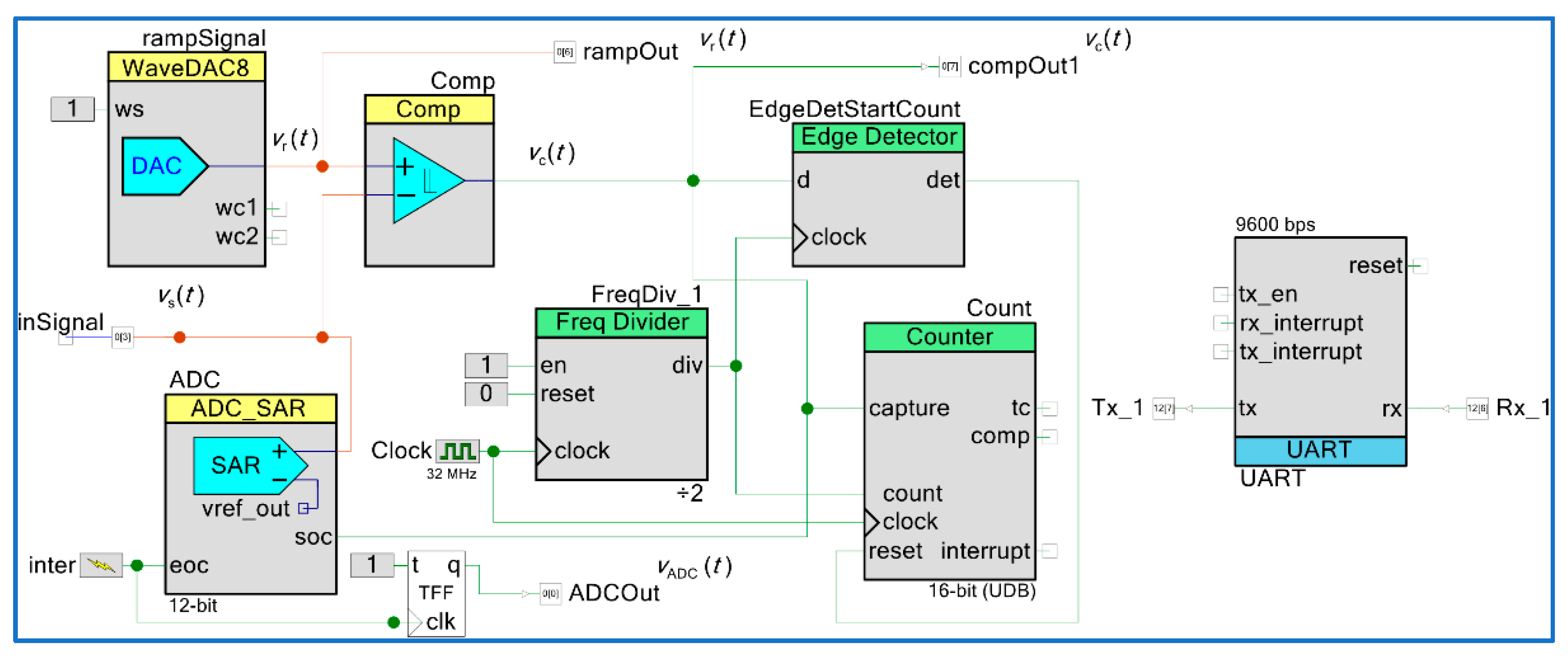
Figure A1 illustrates the internal configuration of the PSoC 5LP used to implement the proposed time-based digitization method in both experimental scenarios. In this architecture, the WaveDAC8 block generates the periodic ramp vr(t), which is compared against the incoming sensor signal vs(t) through the analog comparator; each crossing produces a digital transition that encodes the corresponding timestamp tk.
The comparator output is processed by an edge detector to generate a clean capture pulse, which triggers the 16-bit counter driven by a frequency-divided 16 MHz clock. In parallel, the SAR ADC acquires a conventional 12-bit measurement of the same signal, providing a reference waveform for comparison with the time-encoded reconstruction. Both sets of data are transmitted via UART to a host computer for offline processing using the reconstruction algorithm described in Section 4.1. This implementation mirrors the theoretical architecture presented in Section 3 and enables simultaneous evaluation of amplitude fidelity, timing accuracy, and reconstruction error.
Figure A1.
Internal PSoC 5LP configuration used for the experimental validation. The diagram illustrates the DAC-generated ramp, the analog comparator detecting ramp-crossing events, the frequency divider and counter used for timestamp acquisition, the ADC reference path, and the UART interface for data transmission to the host computer.
Tables A.1 and A.2 summarize the specific configuration parameters used for each of the two experiments. Although the overall signal-chain architecture remains identical, the ramp generator and acquisition settings were adapted to match the characteristics of each signal type.
For the sinusoidal experiment, a 1.25 kHz ramp was selected to provide a high oversampling ratio relative to the 60 Hz electrical waveform, ensuring reliable detection of monotonic crossings.
For the PPG experiment, the ramp frequency was reduced to 80 Hz to align with the slow hemodynamic variations of the physiological signal while maximizing temporal resolution. The tables consolidate the key settings—DAC parameters, comparator mode, timer configuration, ADC sampling, and UART interface—clarifying how the same hardware structure was tailored to two distinct sensing conditions.

Table A1.
PSoC 5LP configuration for the 60 Hz sinusoidal (AC current) experiment.
| Block | Parameter | Configured value | Description / Notes |
| WaveDAC8 (ramp generator) | Output range | VDAC 0 – 4.080 V | Internal DAC range used for ramp generation. |
| Waveform type | Sawtooth | Linear, periodic ramp. | |
| Amplitude | 4.000 Vpp | Approximately 0–4 V swing. | |
| Offset | 2.040 V | Internal offset required by the DAC. | |
| Frequency | 1.250 kHz | Ramp period Tr = 800 μs. | |
| Samples per period | 200 samples | DAC update resolution for the ramp. | |
| Clock source | Internal, 250 kSPS | Built-in sample clock. | |
| Comparator (Comp) | Hysteresis | Enabled | Reduces chatter around the crossing instant. |
| Speed | Fast | Minimizes propagation delay. | |
| Polarity | Non-inverting | Output goes high when v+ > v−. | |
| Sync mode | Bypass | Avoids additional synchronization delay. | |
| Frequency Divider FreqDiv_1) |
Divider | 2 | Divides 32 MHz system clock by 2. |
| Output clock | 16 MHz | Timer tick = 62.5 ns. | |
| Counter (Count, UDB) | Resolution | 16 bits | Time-stamp counter. |
| Period | 65,534 | Free-running up counter. | |
| Clock mode | Up counter | Counts upward continuously. | |
| Capture mode (Advanced) | Rising edge | Captures timer value on comparator edge. | |
| Reload option | On reset | Counter is cleared by firmware reset. | |
| Edge detector (EdgeDetStartCount) | Edge type | Falling edge | Generates a clean pulse for each comparator transition. |
| Resolution | 12 bits | Conventional reference measurement. | |
| Conversion rate | 100 kSPS | As reported by PSoC Creator. | |
| SAR ADC (reference path) | ADC clock | 1.846 MHz (internal) | Derived from internal clock. |
| Sample mode | Hardware trigger | Synchronized with firmware events. | |
| Input range | Vssa–Vdda (single ended) | Direct connection to sensor output. | |
| Reference | External Vref = 2.500 V | Precision voltage reference. | |
| UART | Baud rate | 9600 bps | Transmission of timestamps and ADC samples. |
| Framing | 8-N-1 | 8 data bits, no parity, 1 stop bit. | |
| Current sensor front-end |
Sensor type | YHDC SCT-013-000 | Non-invasive AC current transformer. |
| Nominal range | 0–100 AAC | Mains current measurement. | |
| Turns ratio | 2000:1 | Current-mode secondary. | |
| Burden resistor | 100 Ω | Converts secondary current to voltage. | |
| Measured signal | 60 Hz sinusoidal | Mains-derived current waveform. |
Table A2.
PSoC 5LP configuration for the PPG experiment.
| Block | Parameter | Configured value | Description / Notes |
| WaveDAC8 (ramp generator) | Output range | VDAC 0–4.080 V | Same output range as sinusoidal experiment. |
| Waveform type | Sawtooth | Linear ramp matched to low-frequency PPG dynamics. | |
| Amplitude | 4.000 Vpp | Approximately 0–4 V swing. | |
| Offset | 2.040 V | DAC internal offset. | |
| Ramp frequency | 80 Hz | Ramp period Tr =12.5 ms. | |
| Samples per period | 1250 samples | Higher sample density to ensure ramp linearity at low frequency. | |
| Clock source | Internal, 100 kSPS | Lower sampling rate than sinusoidal experiment due to longer ramp period. | |
| Comparator (Comp) | Hysteresis | Enabled | Identical to sinusoidal experiment. |
| Speed | Fast | Ensures clean detection of slow-varying PPG crossings. | |
| Polarity | Non-Inverting | As in previous experiment. | |
| Sync mode | Bypass | Avoids internal synchronization delay. | |
| Frequency Divider (FreqDiv_1) |
Divider | 2 | Same configuration as sinusoidal experiment. |
| Output clock | 16 MHz | Timer resolution = 62.5 ns. | |
| Counter (Count, UDB) |
Resolution | 16 bits | Time-stamp counter. |
| Period | 65,534 | Free-running. | |
| Clock mode | Up counter | Same behavior as before. | |
| Capture mode | Rising edge | Captures timestamp on comparator event. | |
| Reload option | On Reset | Controlled via firmware. | |
| Edge Detector | Edge type | Falling Edge | Extracts clean comparator transitions for timestamping. |
| SAR ADC (reference) |
Resolution | 12 bits | Used for ADC–ATC comparison. |
| Conversion rate | 100 kSPS | Sufficient for PPG bandwidth. | |
| Sample mode | Hardware trigger | Synchronization with timing logic. | |
| Input range | Vssa–Vdda | Single-ended. | |
| Reference | External Vref = 2.500 V | Ensures ADC reference stability. | |
| UART | Baud rate | 9600 bps | Same interface used to send timestamps and ADC samples. |
| Sensor type | Pulse Sensor (World Famous Electronics) | Reflective optical photoplethysmography module. | |
| Supply voltage | 5 V | Standard operating voltage. | |
| PPG sensor front-end | Output type | Analog, filtered | Outputs amplitude variations proportional to blood volume changes. |
| Placement | Fingertip | Typical physiological measurement site. | |
| Dominant frequency | ~1.2–1.4 Hz | Corresponding to ~72–84 bpm. |
References
- Pallás-Areny, R.; Webster, J.G. Sensor Signal Conditioning, 2nd ed.; Wiley-Interscience: Hoboken, NJ, USA, 2000.
- Abdulhussain, S.H.; Khogali, A.; Yaseen, M.; Oleiwi, Z.S.; Alsharif, M.H.; Abdulhassan, F.F.; Al-bderat, L.; Alarood, A.A. A Comprehensive Review of Sensor Technologies in IoT: Opportunities, Challenges, and Applications. Computers 2025, 14, 342. [CrossRef]
- Javaid, M.; Haleem, A.; Singh, R.P.; Suman, R. Significance of Sensors for Industry 4.0: Roles, Capabilities, and Applications. Sensors and Actuators Reports 2021, 3, 100048. [CrossRef]
- Reverter, F. The art of directly interfacing sensors to microcontrollers. J. Low Power Electron. 2012, 2, 265–281. [CrossRef]
- Puentes-Conde, G.M.; Sifuentes, E.; Molina, J.; Enríquez-Aguilera, F.; Bravo, G.; Navarro-Enríquez, G. Direct Interface Circuits for Resistive, Capacitive, and Inductive Sensors: A Review. Electronics 2025, 14, 2393. [CrossRef]
- Peter, D.; Baker, B.C.; Butler, D.; Darmawaskita, H. Make a Delta-Sigma Converter Using a Microcontroller’s Analog Comparator Module; Microchip Technology Inc.: Chandler, AZ, USA, 1998, 588–593.
- Soldera, J.D.B.; Espindola, M.; Olmos, A. Implementing a 10-Bit Sigma-Delta Analog-to-Digital Converter Using the HC9S08Rx MCUFamilyAnalog Comparator. Free. Semicond. 2005, 1–22. Available online: https://www.nxp.com/docs/en/application note/AN2688.pdf.
- Weber, P.; Windish, C. Build a complete industrial-ADC interface using a microcontroller and a sigma-delta modulator. EDN 2007, 52, 63.
- Integrated ADC for Altera Cyclone-IV Devices, Missing Link Electronics, Technical Brief. 2011. Available online: https: //www.missinglinkelectronics.com/wp-content/uploads/2012/08/MLE-TB20110419.pdf.
- Bengtsson, L. Direct analog-to-microcontroller interfacing. Sens. Actuators A Phys. 2012, 179, 105–113. [CrossRef]
- Grossi, M. Efficient and Accurate Analog Voltage Measurement Using a Direct Sensor-to-Digital Port Interface for Microcontrollers and Field-Programmable Gate Arrays. Sensors 2024, 24, 873. [CrossRef]
- Reverter, F.; Gasulla, M.; Pallàs-Areny, R. Timer-Based Demodulation for Amplitude-Modulated Sensor Signals. IEEE Trans. Instrum. Meas. 2017, 66, 3170–3178. [CrossRef]
- Goldberger, A.L.; Amaral, L.A.N.; Glass, L.; Hausdorff, J.M.; Ivanov, P.C.; Mark, R.G.; Mietus, J.E.; Moody, G.B.; Peng, C.-K.; Stanley, H.E. PhysioBank, PhysioToolkit, and PhysioNet: Components of a New Research Resource for Complex Physiologic Signals. Circulation 2000, 101, e215–e220. [CrossRef]
- BIDMC PPG and Respiration Dataset, PhysioNet, 2019. Available online: https://physionet.org/content/bidmc/1.0.0/.
Figure 1.
Conceptual architecture of the proposed sensor–timer interface based on periodic ramp crossings. The analog sensor signal vs(t) is continuously compared with a locally generated ramp vr(t). Each intersection produces a digital edge that triggers a timer capture event, encoding the analog amplitude as a temporal measurement.
Figure 2.
Timing diagram showing the operation of the time-based digitization process. (Top) Sensor signal vs(t) and periodic ramp vr(t) intersect at discrete instants tk. (Middle) Comparator output pulses marking each crossing event. (Bottom) Reconstructed signal vrec(tk) derived from the time-domain samples.
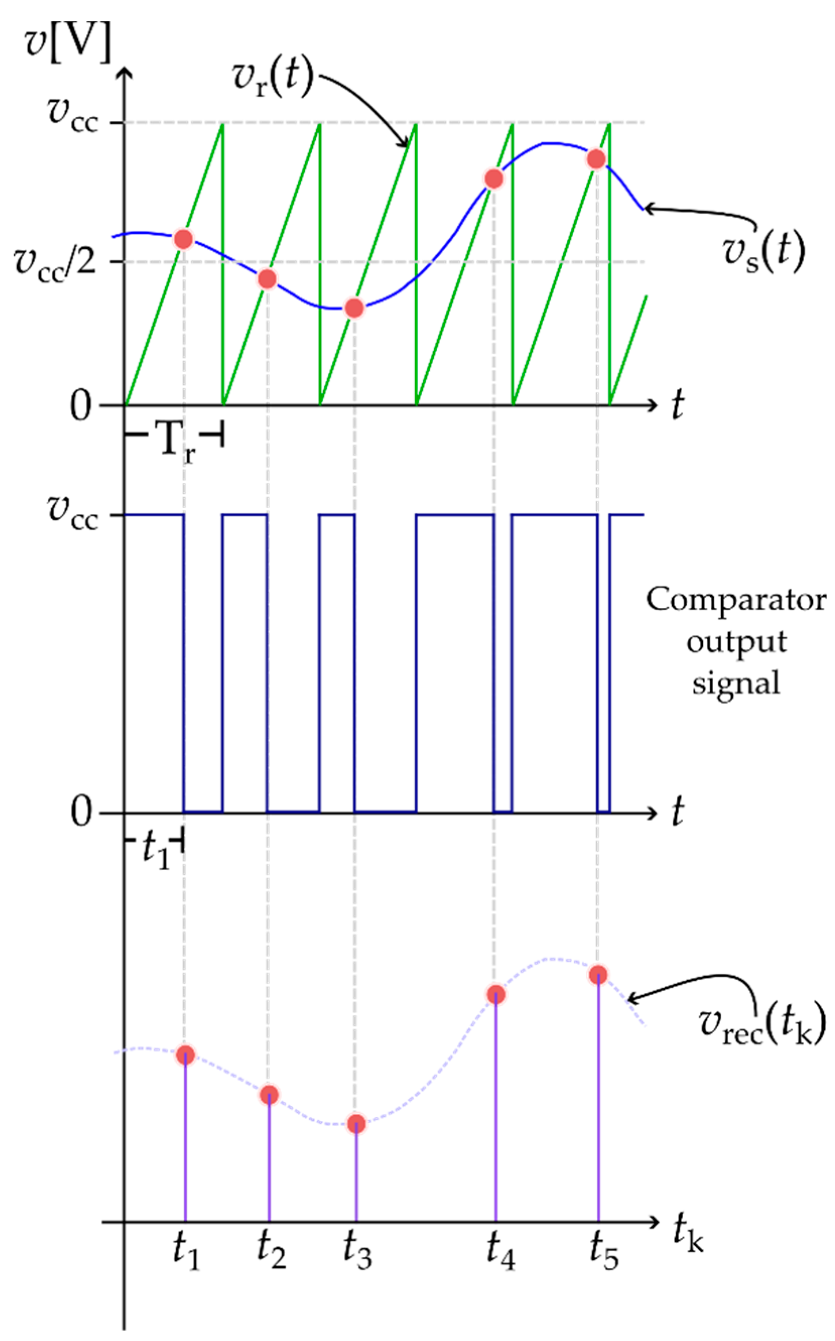
Figure 3.
Experimental setup for the AC–sensor validation: (a) Schematic diagram illustrating the connection between the current transducer, the DAC-generated ramp, the comparator interface, and the timer/capture subsystem on the PSoC 5LP; (b) Photograph of the actual setup, including the PsoC 5LP board, the current sensor clamped to the mains cable, and the resistive heater used as a four-level variable load, with the laptop and oscilloscope for data acquisition and monitoring.
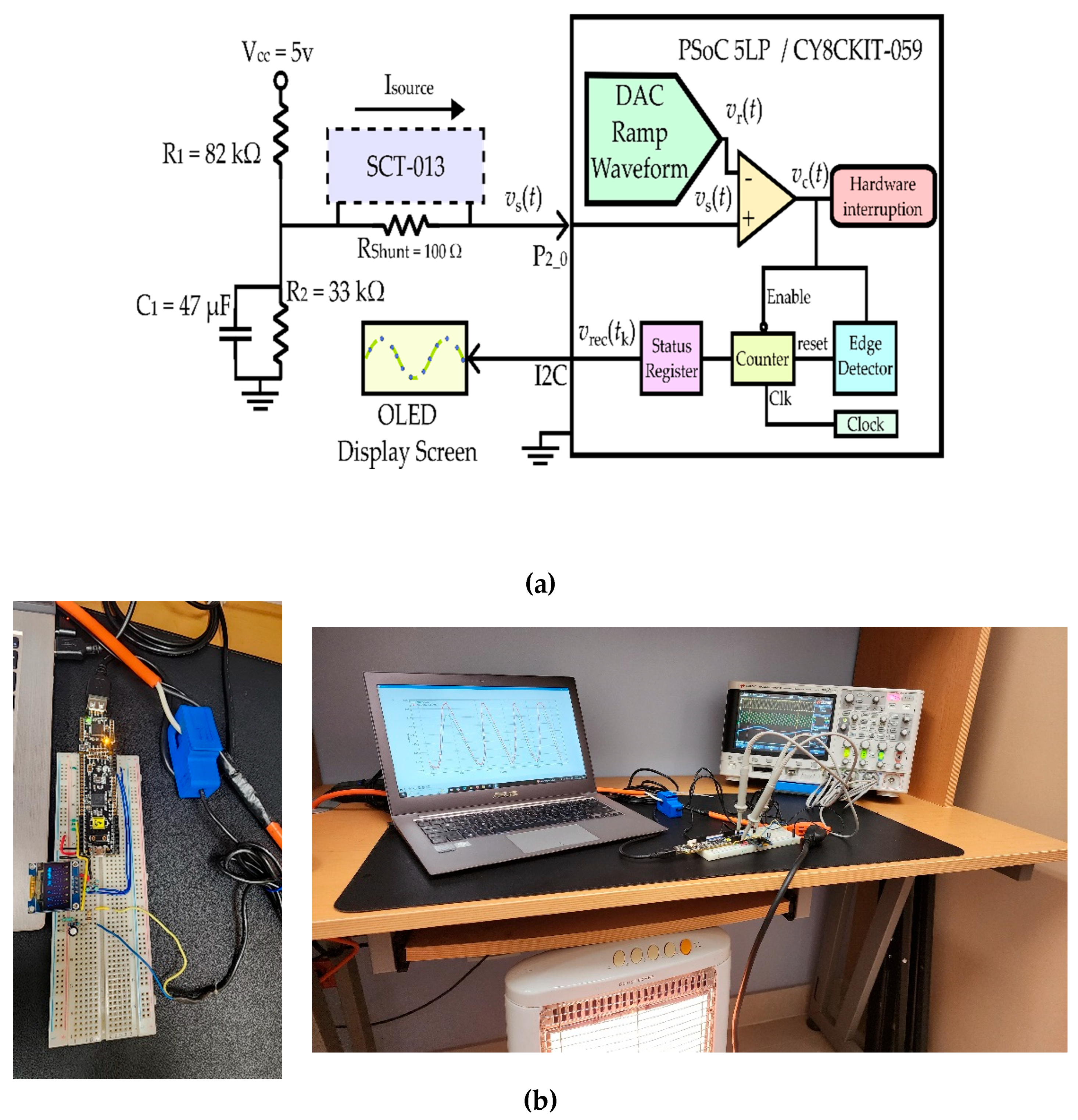
Figure 4.
Experimental setup for the PPG signal acquisition: (a) Schematic diagram illustrating the PPG sensor interface, the DAC ramp generator, the comparator path, and the signal-capture logic used to record timing events; (b) Photograph of the PPG measurement arrangement, showing the PSoC 5LP mounted on the breadboard, oscilloscope probes for monitoring the ramp and sensor signals, and the PPG module placed on the subject’s fingertip.
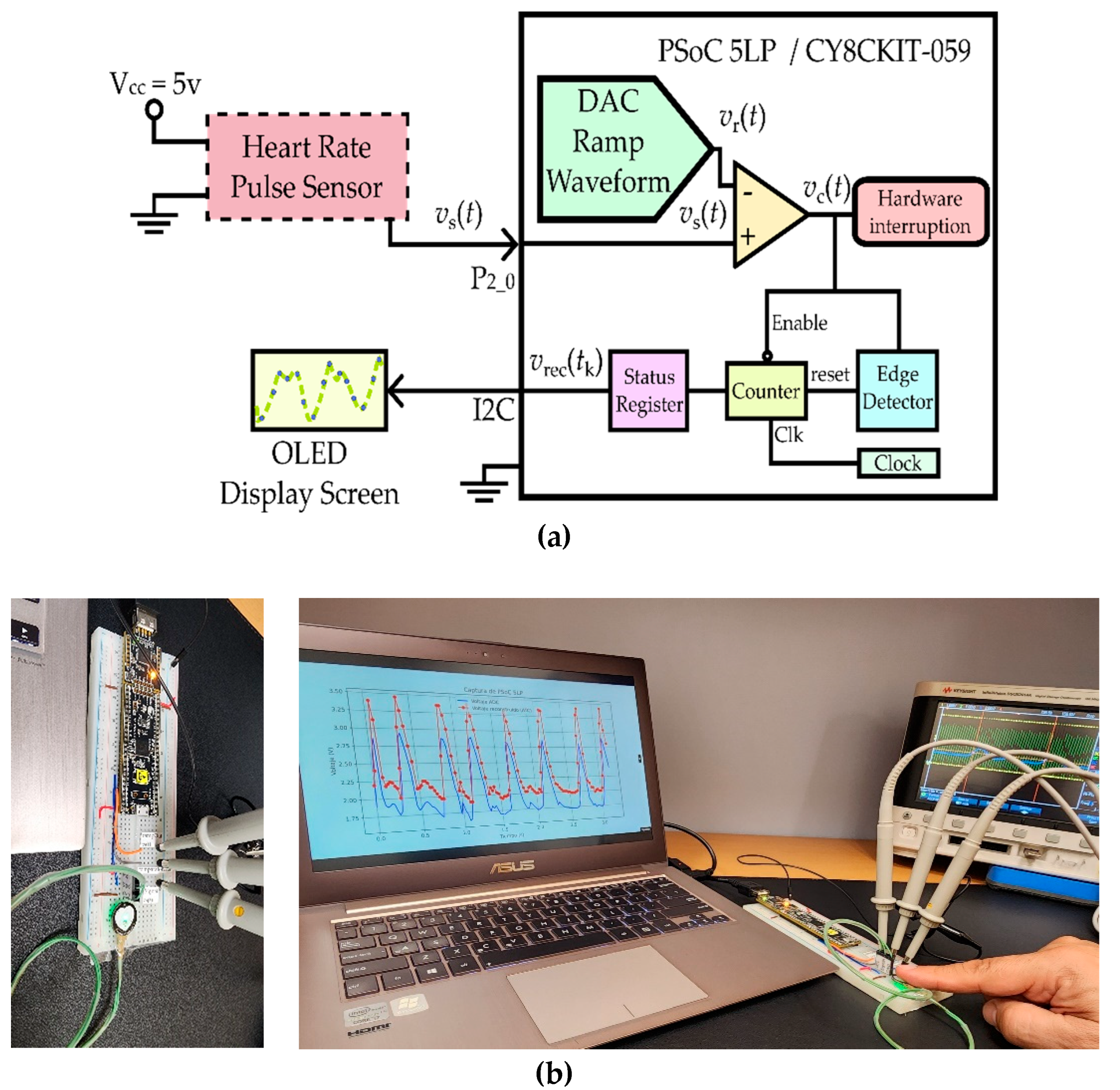
Figure 5.
Simulation results of the proposed time-based digitization method: (a) Sensor signal (60 Hz) and periodic ramp (1 kHz) showing the ramp-crossing instants; (b) reconstructed signal compared with the original analog waveform; (c) instantaneous reconstruction error with RMS bounds.
Figure 5.
Simulation results of the proposed time-based digitization method: (a) Sensor signal (60 Hz) and periodic ramp (1 kHz) showing the ramp-crossing instants; (b) reconstructed signal compared with the original analog waveform; (c) instantaneous reconstruction error with RMS bounds.
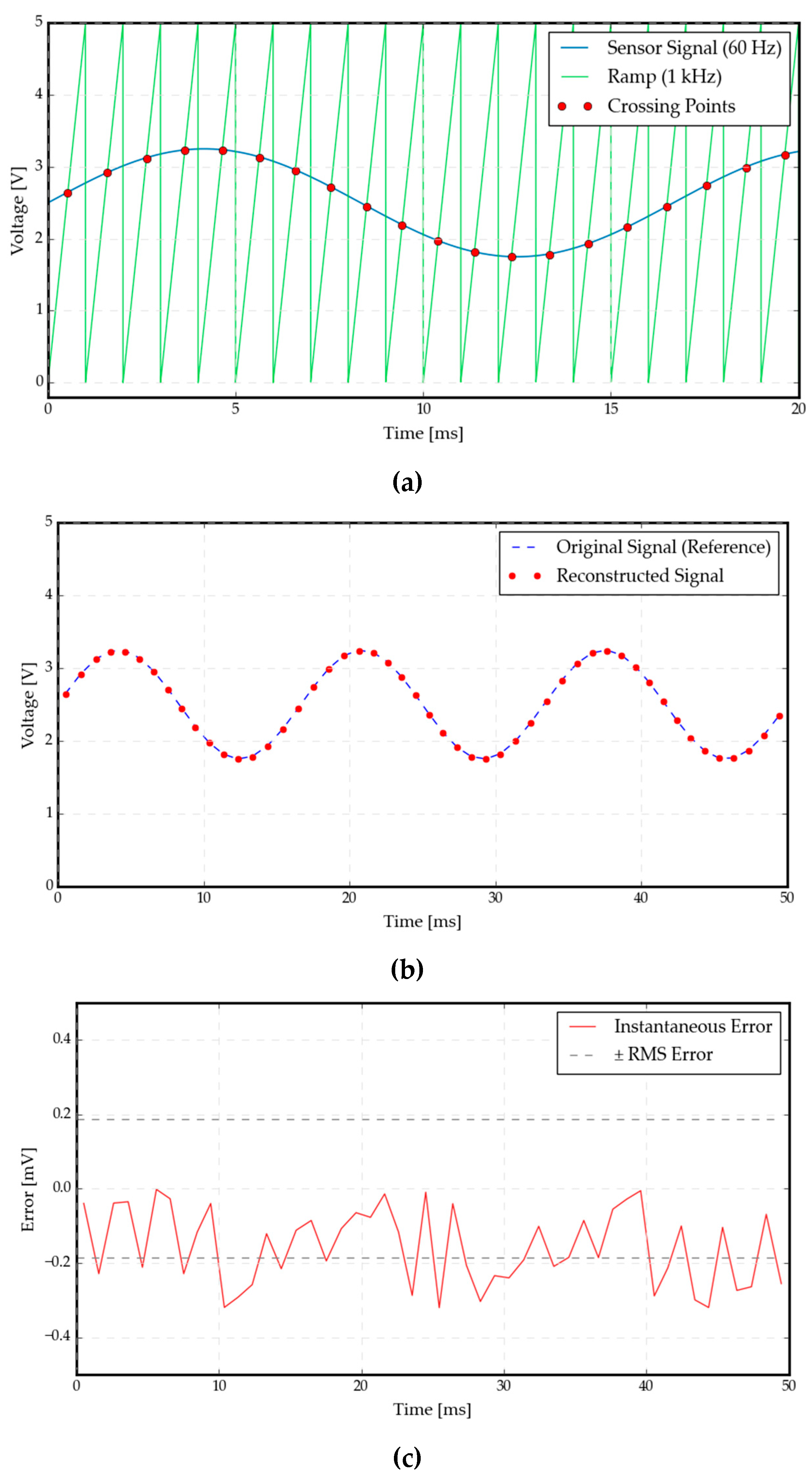
Figure 6.
Simulation results of the proposed time-based digitization method applied to a PPG signal. (a) Photoplethysmographic (PPG) waveform (~1.2 Hz) and the 80 Hz periodic ramp showing the ramp-crossing instants; (b) reconstructed PPG signal (red dots) compared with the original reference waveform (blue dashed line); (c) instantaneous reconstruction error with ±RMS bounds.
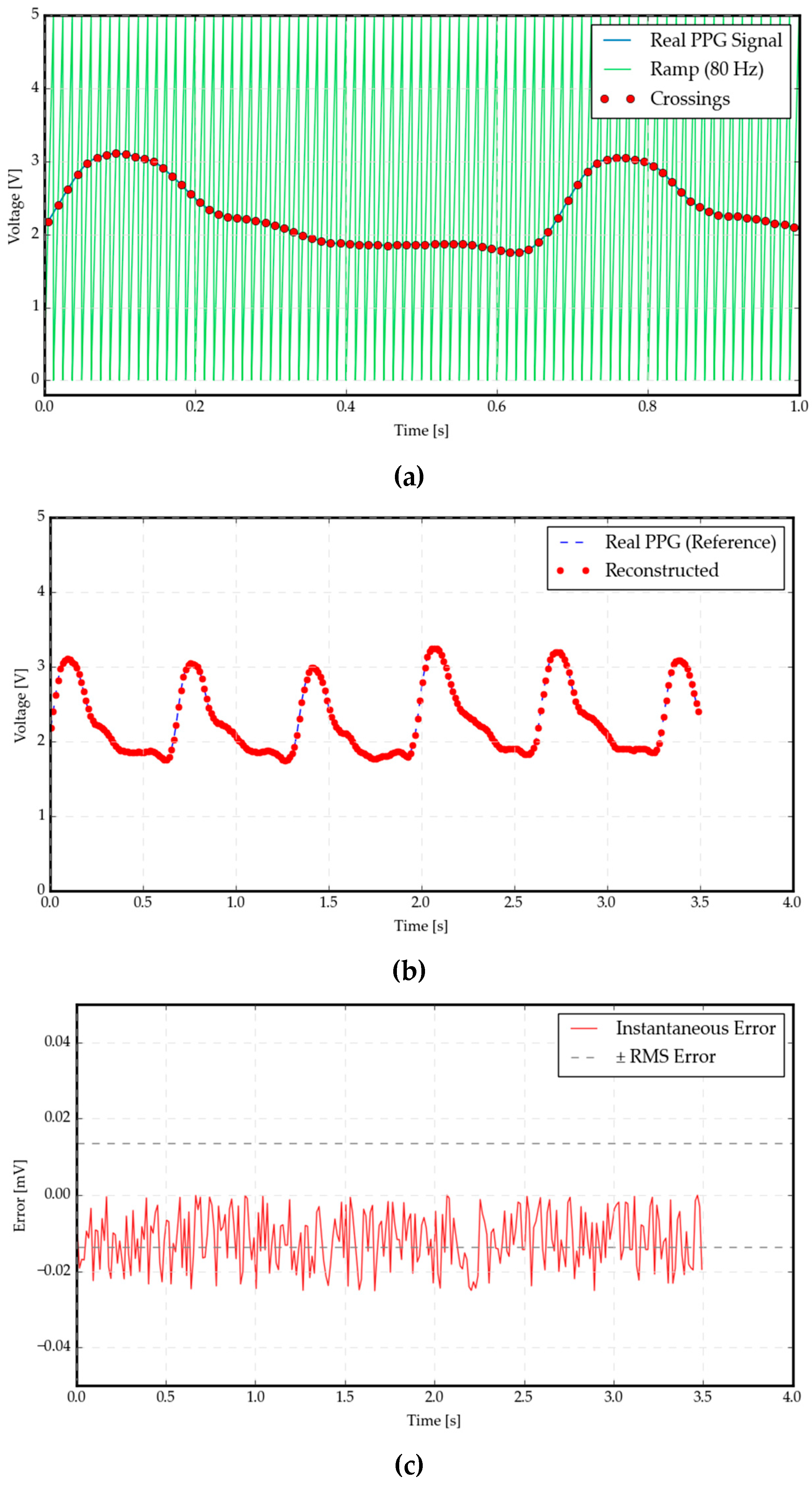
Figure 7.
Experimental results of the proposed time-based digitization method applied to a 60 Hz sinusoidal sensor-signal. (a) Oscilloscope capture showing the sensor waveform, the 1.25 kHz ramp, and the comparator output; (b) Experimental reconstructed sinusoidal waveform (red dots) compared with the 12-bit ADC reference (blue dashed line); (c) instantaneous reconstruction error with ±RMS bounds (RMS = 0.01355 V).
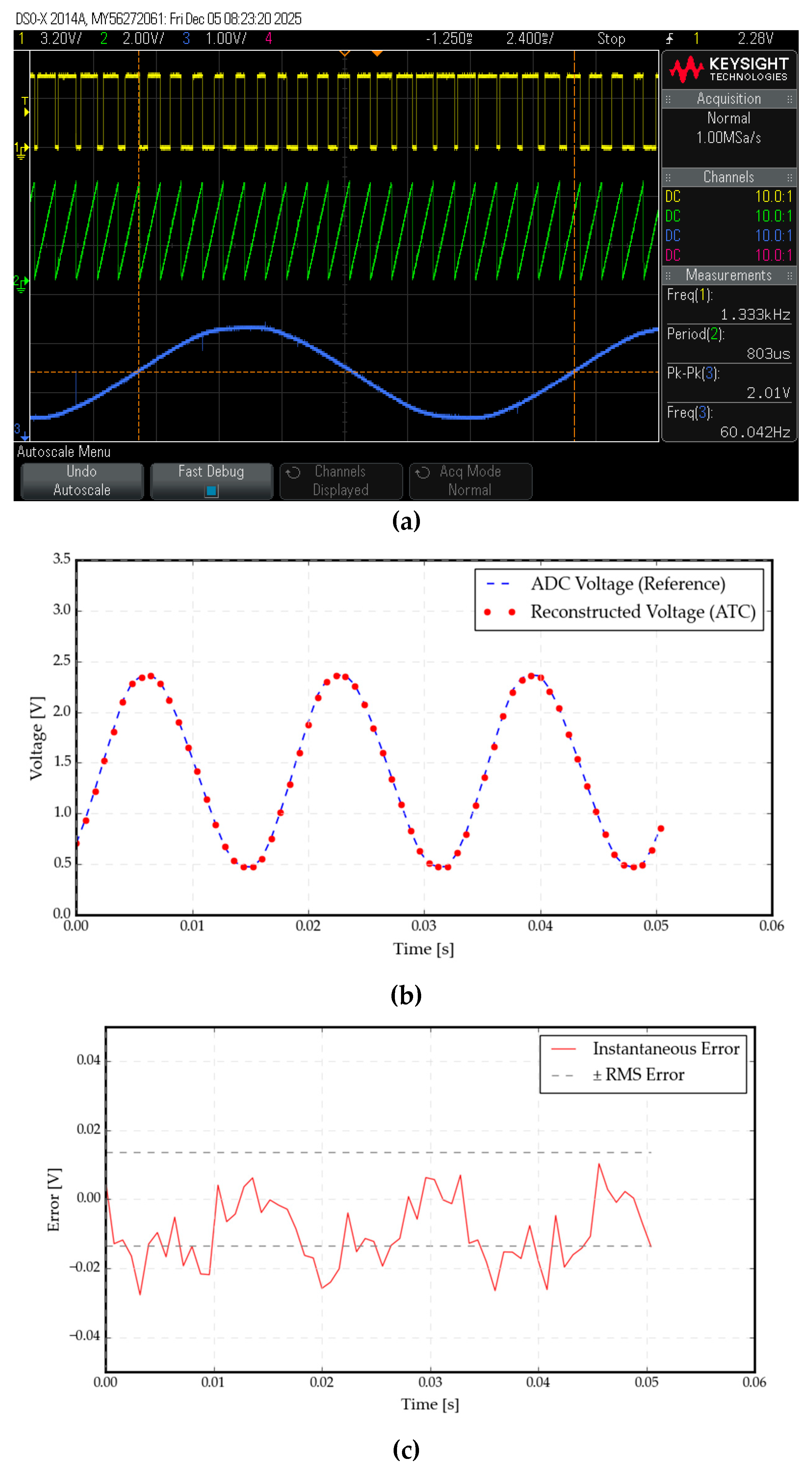
Figure 8.
Experimental results of the proposed time-based digitization method applied to a photoplethysmographic (PPG) sensor signal. (a) Oscilloscope capture showing the PPG waveform, the 80 Hz DAC-generated ramp, and the comparator output used to detect ramp-crossing events; (b) Experimental reconstructed PPG waveform (red dots) compared with the 12-bit ADC reference signal (blue dashed line); (c) Instantaneous reconstruction error with ±RMS bounds (RMS = 0.00778 V).
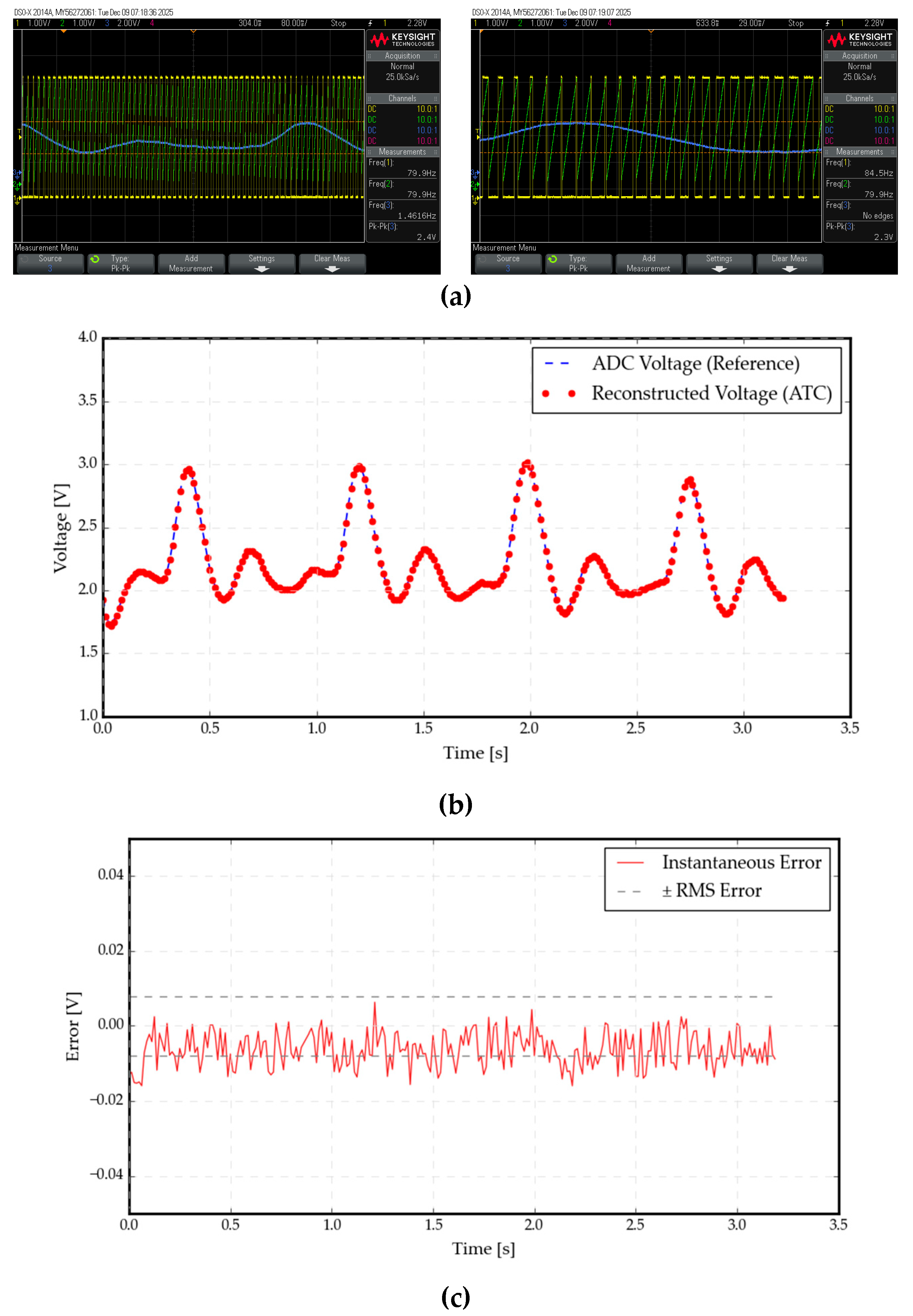
Table 1.
Comparative Summary of ADC-less Direct-Interfacing Techniques.
| Method/ Ref. | Platform | Conversion Principle | Required Hardware | Advantages | Limitations |
| Peter et al. (1998) [6] | PIC16 | First-order ΔΣ loop using a comparator | 2 resistors + capacitor | Simple; flexible input range; minimal external parts | Limited DC accuracy; relies on internal reference |
| Soldera et al. (2005) [7] | HC9S08Rx MCU | Continuous-time ΔΣ | Comparator + RC + timers | ~10-bit resolution; embedded filtering | Low bandwidth; high OSR required |
| Weber & Windish (2007) [8] | MSP430 + AD7400 | External ΔΣ modulator | Dedicated modulator + MCU | Industrial precision; high linearity | Higher cost; external IC required |
| FPGA LVDS DSM (2011) [9] | Altera Cyclone IV | ΔΣ using LVDS as comparator | 2 resistors + capacitor | 60 dB SNR (~10 bits); up to 500 kS/s | Requires HDL design; parameter tuning |
| Bengtsson (2012) [10] | PIC18F458 / FPGA | RC charge/discharge + Schmitt trigger | 2 resistors + capacitor | No ADC or comparator; ~12-bit equivalent | Strongly nonlinear; LUT required; ~65 Hz BW |
| Grossi (2024) [11] | FPGA / MCU | Astable multivibrator; duty cycle | 2 resistors + capacitor | Improved linearity; no pre-charge; no LUT | Limited sampling rate (10–128 Hz) |
| Reverter et al. (2017) [12] | MCU | Triangular-ramp crossing (AM demodulation) | DAC/PWM + comparator | Precise envelope extraction | Not intended for arbitrary waveforms |
| This work | MCU | Sawtooth ramp-crossing time encoding | PWM/DAC + comparator + timer | Single crossing; constant slope; linear mapping; higher efficiency | Requires a stable ramp |
Disclaimer/Publisher’s Note: The statements, opinions and data contained in all publications are solely those of the individual author(s) and contributor(s) and not of MDPI and/or the editor(s). MDPI and/or the editor(s) disclaim responsibility for any injury to people or property resulting from any ideas, methods, instructions or products referred to in the content. |
© 2025 by the authors. Licensee MDPI, Basel, Switzerland. This article is an open access article distributed under the terms and conditions of the Creative Commons Attribution (CC BY) license (https://creativecommons.org/licenses/by/4.0/).
Copyright: This open access article is published under a Creative Commons CC BY 4.0 license, which permit the free download, distribution, and reuse, provided that the author and preprint are cited in any reuse.


