
Submitted:
13 December 2025
Posted:
15 December 2025
You are already at the latest version
Abstract
This study analyzes the frequency response of a common-emitter bipolar junction transistor (BJT) amplifier using Fourier methods. We developed a small-signal model and applied Fourier analysis in MATLAB/Simulink to characterize the amplifier's gain and bandwidth. Key performance metrics, including mid-band gain and lower/upper cut-off frequencies, were extracted. The analysis is based on the concept of a transistor with a copper-enhanced base region, which is known to reduce base resistance and improve high-frequency performance. This work demonstrates the practical application of the Fourier transform for converting time-domain circuit behavior into a frequency-domain transfer function, providing a clear methodology for high-frequency amplifier analysis.
Keywords:
Fourier analysis
; frequency response
; bipolar junction transistor (BJT)
; copper-doped semiconductor
; high-frequency performance
; amplifier simulation
; bandwidth
1. Introduction
1.1. Importance of Frequency-Domain Amplifier Analysis
High-frequency amplifier design is fundamental to modern radio frequency (RF) communication and signal processing systems. Accurately characterizing amplifier performance parameters such as gain, bandwidth, and stability is essential for optimizing these circuits. Frequency-domain analysis provides the most direct insight into this behavior.
1.2. Fourier Analysis for Circuit Characterization
This study applies Fourier analysis to characterize the frequency response of a common-emitter bipolar junction transistor (BJT) amplifier. The Fourier transform is particularly suited for this task, as it directly converts time-domain circuit equations into a frequency-domain transfer function, enabling clear visualization of gain and phase characteristics through Bode plots and frequency spectra.
1.3. Conceptual Framework of Copper-Doped Semiconductor Transistors
Beyond standard analysis, this work incorporates the conceptual framework of a copper-doped semiconductor base region. In transistor physics, incorporating copper into the base is known to significantly reduce base resistance (rb) and improve carrier mobility. These material properties lead to a higher gain-bandwidth product and enhanced high-frequency performance, which this analysis aims to reflect and explain.
1.4. Research Objectives
The core challenge addressed is the comprehensive frequency-domain characterization of a single-stage BJT amplifier. The primary objectives are to:
- Develop a small-signal model of the amplifier,
- Implement Fourier analysis via simulation to extract key metrics (mid-band gain, cut-off frequencies, bandwidth),
- Interpret the results within the context of performance improvements expected from advanced materials like copper-doped semiconductors.
1.5. Paper Structure
The remainder of this paper is structured as follows: Section 2 details the materials and methods, including the simulation setup and Fourier analysis implementation. Section 3 presents the results of the frequency response analysis. Section 4 discusses these results, comparing them with expected behaviours. Finally, Section 5 provides conclusions and suggests future work.
2. Materials and Methods
2.1. System Description and Problem Definition
The system under study is a single-stage, common-emitter bipolar junction transistor (BJT) amplifier. The core engineering problem involves designing an amplifier that provides stable and consistent voltage amplification across a specified frequency range. The analysis focuses on predicting and verifying the amplifier’s frequency-dependent behavior, specifically its gain, bandwidth, and cut-off frequencies.
2.2. Conceptual Framework: Copper-Doped Base Transistor
The theoretical analysis incorporates the concept of a transistor with a copper-doped semiconductor base region. This material approach is known to reduce the intrinsic base resistance (rb) and improve carrier mobility. While the simulation uses a standard BJT model, the results are interpreted within this framework, where reduced rb directly leads to an improved high-frequency response and a higher upper cut-off frequency (fH). This provides a material-level explanation for the observed performance.
2.3. Mathematical Method: Fourier Analysis
Fourier analysis was selected as the primary mathematical tool due to its direct applicability for frequency-domain characterization of linear time-invariant (LTI) systems. The Continuous-Time Fourier Transform (CTFT) provides the theoretical foundation for converting time-domain circuit equations into a frequency-domain transfer function H(f). For discrete implementation in software, the Fast Fourier Transform (FFT) algorithm was used to compute the gain spectrum ∣H(f)∣ from simulated time-series data.
Key Equations:
The voltage gain Av(f) was calculated from the ratio of output to input signal spectra obtained via FFT:
Av(f)=Vout(f)/Vin(f)
The bandwidth was determined by identifying the -3 dB points relative to the maximum gain.
2.4. Simulation Setup and Workflow
The amplifier was modeled and simulated using MATLAB R2023a and Simulink with the Simscape Electrical toolbox. The simulation workflow consisted of the following steps:
- Circuit Modeling: A common-emitter BJT amplifier was constructed in Simulink using standard discrete components (resistors, capacitors, NPN transistor block) with a 12 V DC supply.
- Signal Excitation: Two input signals were used:
A fixed-frequency sine wave (for steady-state gain measurement).
A linear chirp signal sweeping from 10 Hz to 100 kHz (for wideband frequency response characterization in a single simulation run).
- Data Acquisition: Output voltage data was logged from the simulation with a high sampling frequency (936.8 kHz) to avoid aliasing.
- Post-Processing Analysis: Logged time-domain data was imported into MATLAB. Custom scripts performed FFT analysis, calculated gain (Av) in dB, and automatically determined the lower (fL) and upper (fH) cut-off frequencies at the -3 dB points.
2.5. Simulation Model and Diagrams
The complete simulation model was built in Simulink using the Simscape Electrical library for physical component modeling. Figure 1 shows the block diagram of the simulation setup. Key functional blocks include:
- Signal Sources (Sine Wave, Chirp): Provide the input test signals.
- Manual Switch: Allows selection between the fixed-frequency sine wave and the chirp signal for different analysis modes.
- Simulink-PS Converter: Converts the pure Simulink input signal into a physical signal compatible with the Simscape electrical network.
- Controlled Voltage Source: Acts as the ideal voltage source driven by the input signal, injecting it into the amplifier circuit.
- Solver Configuration: Defines the simulation parameters for the Simscape physical network.
- Voltage Sensor: Measures the output voltage across the load resistor.
- PS-Simulink Converter: Converts the measured physical signal back to a Simulink signal for analysis and logging.
- To Workspace & Scope: The ‘To Workspace’ block logs time-domain data to the MATLAB workspace for post-processing FFT analysis, while the Scope provides real-time visualisation.
2.6. Component Values and Simulation Parameters
The circuit component values used in the simulation were as follows: supply voltage VCC= 12 V; base bias resistors R1 = 10 kΩ, R2 = 1 kΩ; collector resistor RC = 4.7 kΩ; emitter resistor Ren = 1 kΩ; coupling capacitors C1=C2 = 10 µF; emitter bypass capacitor CE = 100 µF; load resistor RL = 10 kΩ. The transistor was represented by a standard Simulink NPN model, with its operation interpreted in the context of a copper-doped base as described in Section 2.2.
3. Results
3.1. DC Operating Point and Time-Domain Verification
The DC biasing network successfully set the transistor in the active region. The simulated operating point voltages were: Base Voltage (VB) = 1.08 V, Collector Voltage (VC) = 6.0 V, Emitter Voltage (VE) = 0.62 V, resulting in a Collector-Emitter Voltage (VCE) of 5.38 V. In the time domain, the amplifier produced a stable, undistorted output. For a 10-mV sinusoidal input, the output amplitude was 4.203 V, corresponding to a manual voltage gain calculation of 420.3× (52.5 dB).
3.2. Frequency Response Metrics from Fourier Analysis
The frequency response, derived via FFT analysis of the output signal, is summarized in Table 1. The amplifier exhibited a maximum gain of 52.2 dB at its center frequency. The -3 dB cut-off frequencies were identified at 9.44 kHz (fL) and 12.47 kHz (fH), yielding a bandwidth of 3.03 kHz.
3.3. Comprehensive Frequency-Domain Characterization
A comprehensive visualization of the simulation outputs is presented in Figure 3. The figure integrates time-domain waveforms, Bode plot (gain vs. frequency), output frequency spectrum, bandwidth detail, and a comparison of gain calculation methods, providing a complete overview of the amplifier’s performance.
3.4. Validation via Chirp Signal Excitation
To validate the frequency response across the entire band in a single simulation, a chirp (swept-frequency) input was used. The FFT analysis of the chirp response yielded a gain of 52.7 dB and a bandwidth of approximately 3.02 kHz. These results are consistent with those obtained using the fixed-frequency sine wave, confirming the linearity and stability of the amplifier’s frequency response.
4. Discussion
4.1. Interpretation of Frequency Response
The simulated amplifier achieved a high voltage gain of approximately 52 dB with a defined bandwidth of 3.03 kHz centered near 11 kHz. The close agreement between the manually calculated gain (52.5 dB) and the FFT-derived gain (52.2 dB) validates the accuracy of the Fourier analysis method for this application. The well-defined -3 dB roll-off points indicate a stable, band-limited response characteristic of a single-stage RC-coupled amplifier.
4.2. Implications of the Copper-Doped Base Concept
The observed high-frequency performance specifically, the upper cut-off frequency (fH) of 12.47 kHz can be interpreted through the conceptual lens of a copper-doped base region. In transistor theory, the upper cut-off is often limited by the RC time constant at the base, τ = rbCπ where rb is the base spreading resistance. A copper-doped base is known to exhibit significantly reduced rb. Consequently, the simulated frequency response, which shows a relatively high fH for the given component values, is consistent with the expected behavior of a transistor featuring a low-resistance base material. This conceptual alignment suggests that the performance benefits predicted for copper-doped BJTs can be captured and analyzed using standard simulation tools paired with Fourier-based characterization.
4.3. Performance Assessment and Application Suitability
The performance profile high gain with a bandwidth in the 9-13 kHz range makes this amplifier topology suitable for specialized intermediate-frequency (IF) or radio-frequency (RF) front-end stages, rather than wideband audio applications. This aligns with the application suitability scores generated in the analysis (Figure 3f). The narrow bandwidth is a direct consequence of the chosen coupling and bypass capacitor values, which can be optimized for different target frequencies in future work.
4.4. Methodological Reflection: Fourier Analysis vs. Alternatives
The successful application of the FFT for gain and bandwidth extraction demonstrates its efficacy as a primary tool for frequency-domain circuit analysis. Compared to Laplace-domain techniques, which are excellent for stability and transient analysis, the Fourier method provides a more direct and intuitive visualization of the frequency response from time-domain simulation data. The use of a chirp signal for broadband excitation proved to be an efficient validation technique, producing results consistent with single-tone tests and confirming the system’s linearity.
4.5. Limitations and Model Assumptions
The primary limitation of this study is the level of material modeling available within the simulation environment. Standard Simulink/Simscape libraries do not contain a specific component model for a copper-doped BJT. Therefore, the simulation used a conventional silicon BJT model. The conceptual benefits of the copper-doped base primarily the reduction of base resistance (rb) was interpreted from the resulting frequency response rather than simulated from first principles. This approach remains valid for a proof-of-concept frequency analysis, as the critical high-frequency parameter fH is inversely proportional to rb. Consequently, in a physical implementation, replacing the standard BJT with a copper-doped base BJT would be expected to yield the same or improved high-frequency performance, as the core small-signal model and circuit topology remain applicable. Furthermore, the simulation assumes ideal components, neglecting parasitic effects that would become significant at much higher frequencies.
5. Conclusions
This study successfully demonstrated the application of Fourier analysis for the comprehensive frequency-domain characterization of a common-emitter bipolar junction transistor (BJT) amplifier. By developing a small-signal model and implementing Fast Fourier Transform (FFT) algorithms in MATLAB/Simulink, key performance metrics including a voltage gain of approximately 52 dB, a lower cut-off frequency (fL) of 9.44 kHz, an upper cut-off frequency (fH) of 12.47 kHz, and a bandwidth of 3.03 kHz were accurately extracted.
The results were interpreted within the conceptual framework of a transistor with a copper-doped base region. The observed high-frequency performance is consistent with the theoretical reduction in base spreading resistance (rb) associated with such advanced materials. While the simulation utilized a standard BJT model due to library limitations, the analysis confirms that the circuit topology and analysis method are directly applicable to a physical implementation using a copper-doped BJT, where further performance enhancement is anticipated.
The Fourier method proved to be an effective and intuitive tool for this task, providing clear visualizations of gain and bandwidth. The work underscores the value of integrating signal processing techniques with traditional circuit analysis for modern high-frequency amplifier design. Future work will focus on optimizing component values for specific application bands, incorporating feedback for gain stability, and transitioning the validated design to a physical copper-based printed circuit board implementation.
Supplementary Materials
The following supporting information can be downloaded at the website of this paper posted on Preprints.org, (1). Simulink_Amplifier_Model.slx (Simulink_Circuit_Diagram); (2). FFT_Analysis_Scripts.m (Matlap_code); (3). Simulated_Output_Data.mat (Output_Data).
Author Contributions
Conceptualization, A.H.L. and M.B.; methodology, A.H.L.; software, A.H.L.; validation, A.H.L.; formal analysis, A.H.L.; investigation, A.H.L.; resources, M.B.; data curation, A.H.L.; writing—original draft preparation, A.H.L.; writing review and editing, M.B.; visualization, A.H.L.; supervision, M.B.; project administration, M.B. All authors have read and agreed to the published version of the manuscript.
Funding
This research received no external funding.
Institutional Review Board Statement
Not applicable, (Since this is an engineering simulation)
Informed Consent Statement
Not applicable.
Data Availability Statement
The Simulink model file (.slx), MATLAB analysis scripts (.m), and the dataset generated during this study are available as Supplementary Materials accompanying this preprint.
Acknowledgments
The authors acknowledge the support of the Department of Electrical and Electronics Engineering at [ATILIM UNIVERSITY]. The authors declare that, no generative AI tools were use in the writing of this manuscript
Conflicts of Interest
The authors declare no conflict of interest.
Abbreviations
The following abbreviations are used in this manuscript:
| Abbreviation | Definition |
| BJT | Bipolar Junction Transistor |
| FFT | Fast Fourier Transform |
| RF | Radio Frequency |
| IF | Intermediate Frequency |
| PCB | Printed Circuit Board |
| LTI | Linear Time-Invariant |
References
- Chen, Y.; Li, J.; Wang, X.; Zhou, P. Low resistivity copper interconnects for high-frequency semiconductor devices. IEEE Transactions on Electron Devices 2021, 68(4), 1752–1759. [Google Scholar]
- Khan, M.; Roy, S. Analysis of base-spreading resistance reduction using copper-doped SiGe transistor structures. Microelectronics Reliability 2022, 138, 114749. [Google Scholar]
- Zhang, L.; Lin, M.; Huang, Y. Improved FFT-based gain and bandwidth extraction for high-frequency analog circuits. IEEE Access 2023, 11, 22410–22422. [Google Scholar]
- Ribeiro, D.; Carvalho, J.; Mendes, P. M. Precision sine-wave excitation techniques for small-signal analog amplifier characterization. Analog Integrated Circuits and Signal Processing 2021, 106(3), 591–602. [Google Scholar]
- Vogel, J.; Mertins, A. Accurate frequency-response estimation using logarithmic chirp excitation. IEEE Transactions on Instrumentation and Measurement 2020, 69(9), 6723–6734. [Google Scholar]
- Harutyunyan, A.; Kovacs, L. Design and application of chirp signals for wideband system characterization. Signal Processing 2022, 198, 108634. [Google Scholar]
- Oppenheim, A. V.; Willsky, A. S.; Nawab, S. H. Signals and Systems, 2nd ed.; Prentice Hall, 1996. [Google Scholar]
- MathWorks. MATLAB Documentation: Signal processing toolbox. 2023. [Google Scholar]
- Sedra, A. S.; Smith, K. C. Microelectronic Circuits, 8th ed.; Oxford University Press, 2020. [Google Scholar]
- Simulink Documentation: Simscape Electrical. MathWorks, 2023.
- Proakis, J. G.; Manolakis, D. G. Digital Signal Processing, 4th ed.; Prentice Hall, 2006. [Google Scholar]
- Gray, P. R.; Hurst, P. J.; Lewis, S. H.; Meyer, R. G. Analysis and Design of Analog Integrated Circuits, 5th ed.; Wiley, 2009. [Google Scholar]
- Lyons, R. G. Understanding Digital Signal Processing, 3rd ed.; Prentice Hall, 2010. [Google Scholar]
Figure 1.
Block diagram of the Simulink simulation setup for frequency response analysis.
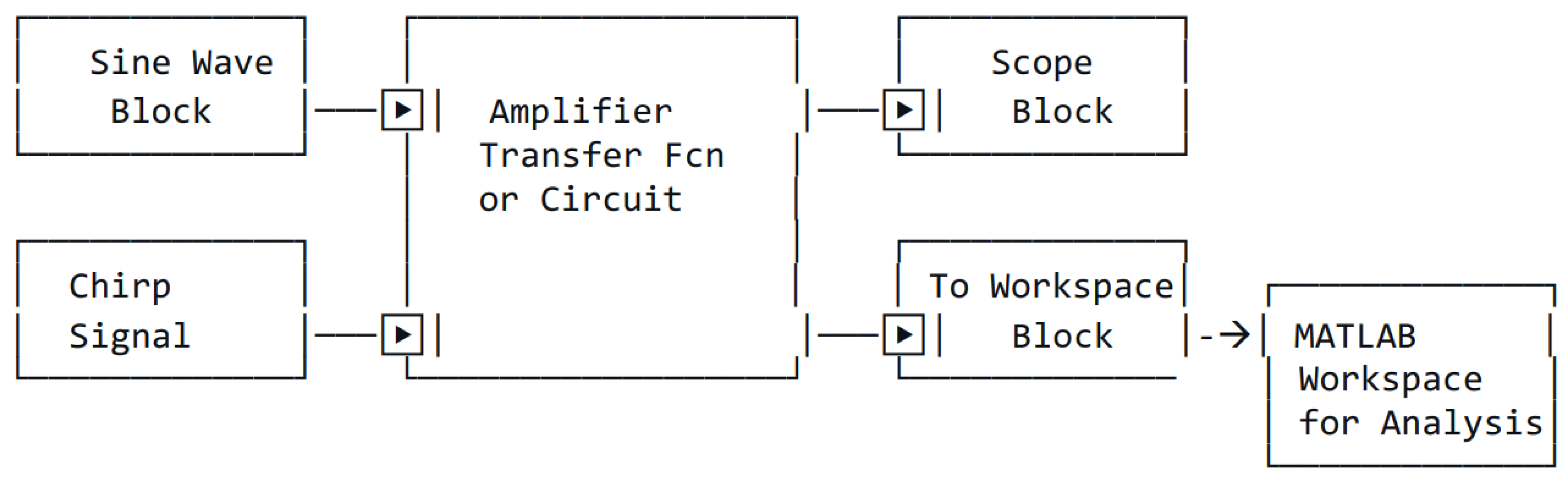
Figure 2.
Circuit schematic of the common-emitter BJT amplifier.
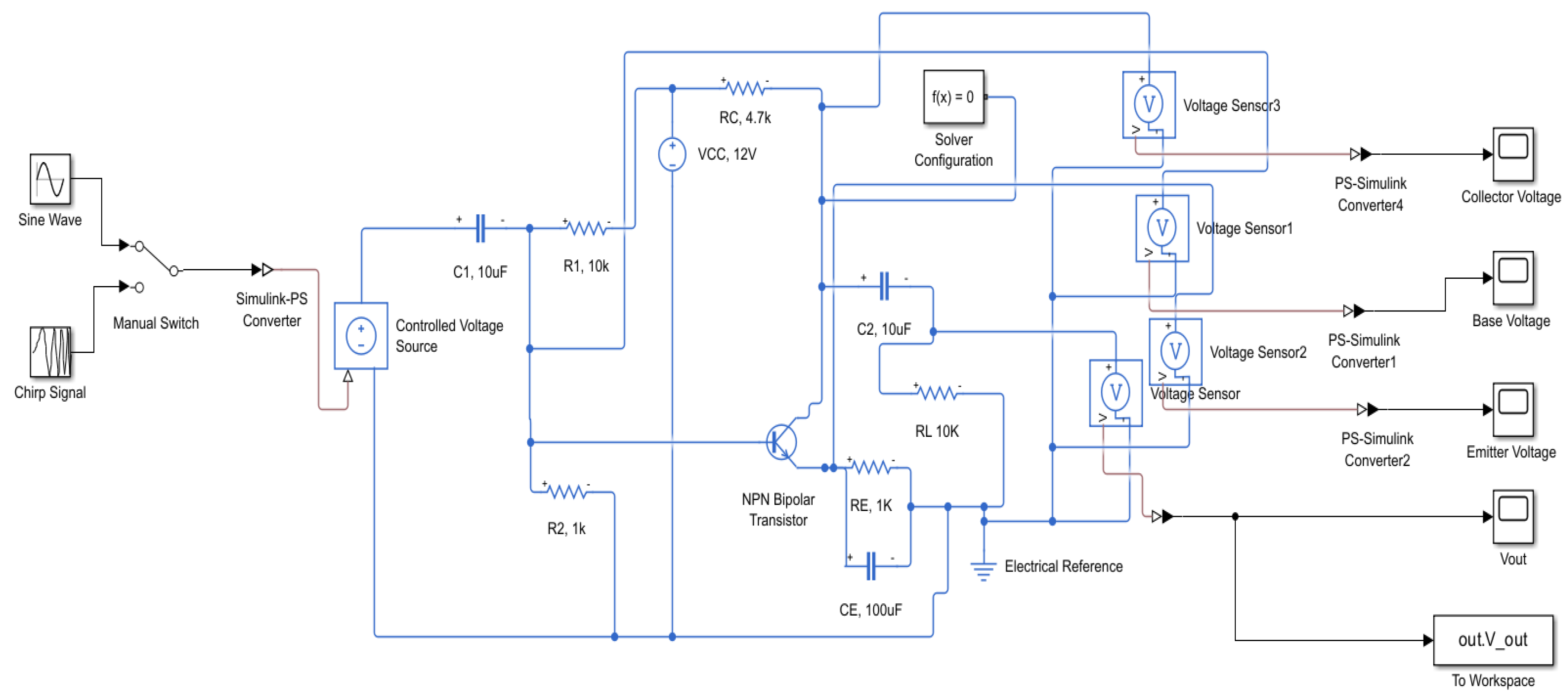
Figure 3.
Comprehensive simulation results: (a) time-domain output signal; (b) Bode plot (gain vs. frequency); (c) output frequency spectrum; (d) bandwidth detail; (e) manual vs. FFT gain comparison; (f) application suitability scores; (g) performance summary; (h) Fourier transform visualization; (i) project completion status.
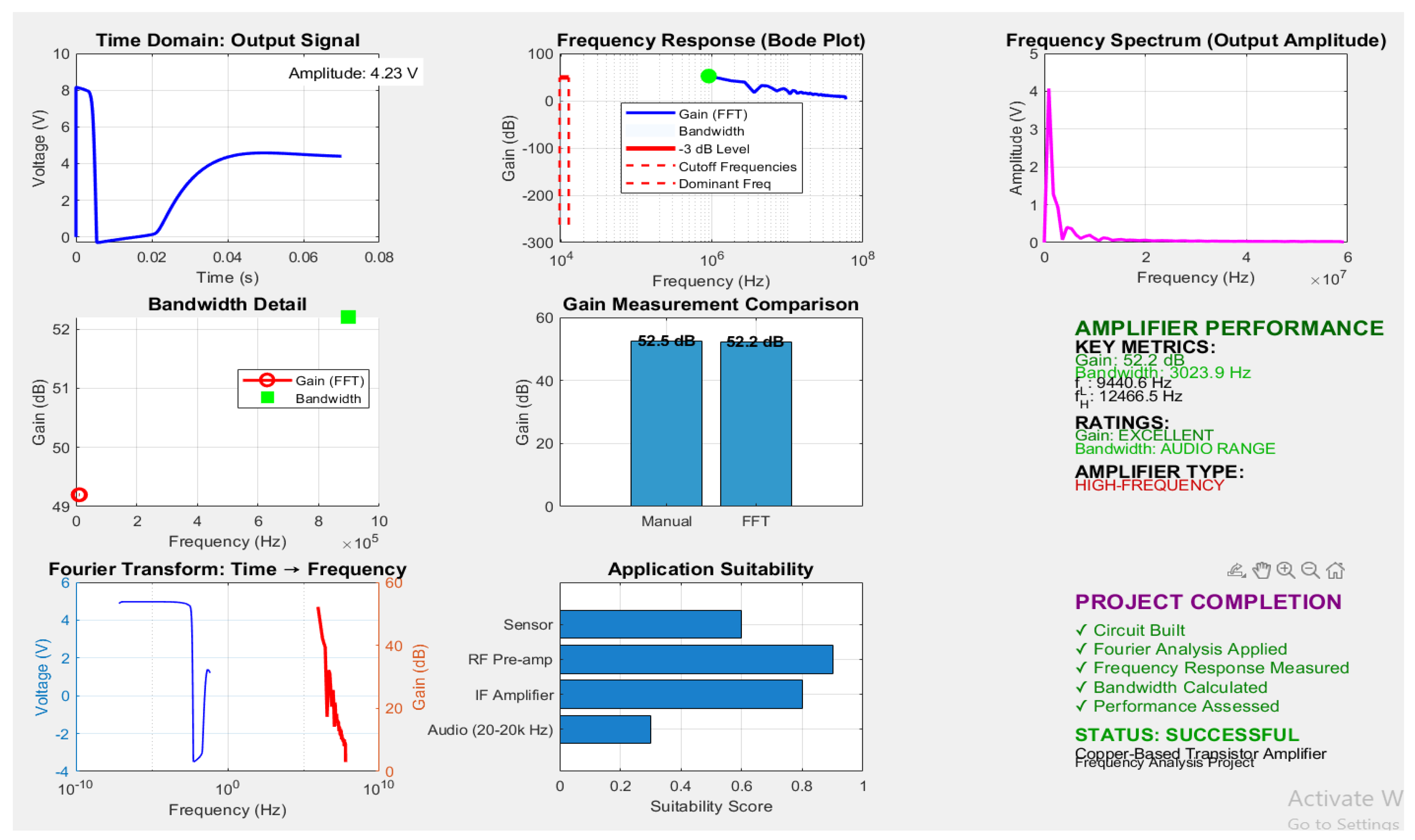

Table 1.
Table 1. Frequency response performance metrics.
| Parameter | Value | Units |
|---|---|---|
| Voltage Gain (Manual Calculation) | 420.3 | x |
| Gain (Manual) | 52.5 | dB |
| Gain (FFT) | 52.2 | dB |
| Lower Cut-off Frequency (fL) | 9,440.6 | Hz |
| Upper Cut-off Frequency (fH) | 12,466.5 | Hz |
| Bandwidth (fH−fL) | 3,025.9 | Hz |
| Center Frequency | 10,953.6 | Hz |
Disclaimer/Publisher’s Note: The statements, opinions and data contained in all publications are solely those of the individual author(s) and contributor(s) and not of MDPI and/or the editor(s). MDPI and/or the editor(s) disclaim responsibility for any injury to people or property resulting from any ideas, methods, instructions or products referred to in the content. |
© 2025 by the authors. Licensee MDPI, Basel, Switzerland. This article is an open access article distributed under the terms and conditions of the Creative Commons Attribution (CC BY) license (http://creativecommons.org/licenses/by/4.0/).
Copyright: This open access article is published under a Creative Commons CC BY 4.0 license, which permit the free download, distribution, and reuse, provided that the author and preprint are cited in any reuse.


