
Submitted:
10 December 2025
Posted:
10 December 2025
You are already at the latest version
Abstract
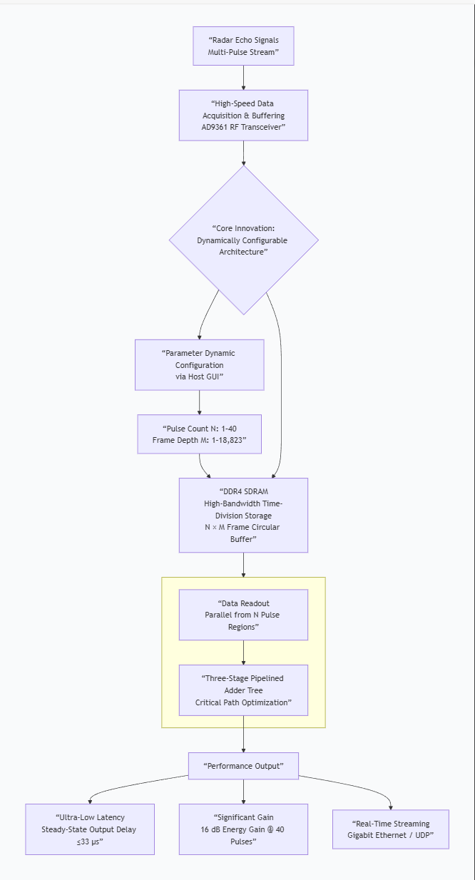
Radar signal coherent integration technology is a critical method to improve the performance of detection systems. However, existing techniques face challenges regarding real-time performance and the flexibility of multi-pulse coherent accumulation. In this paper, a dynamically configurable multi-pulse multi-frame real-time coherent integration system based on FPGA is designed and implemented, and the dynamic configuration of the number of pulses and the number of frames stored for each pulse is realized through the host computer. The experimental results show that the output signal delay of coherent integration is 33 microseconds at 40 pulses, and the energy gain reaches 16 dB at 40 pulses, which provides a dynamically configurable hardware platform and solution for real-time coherent integration of high-frame-count, multi-pulse radar signals.
Keywords:
radar detection
; coherent integration
; FPGA
; dynamic configuration
1. Introduction
Coherent accumulation has become a critical technique in modern radar and
communication systems for combating channel fading and enhancing the detection of weak signals [1,2,3]. By integrating multiple radar pulse echoes before detection, this technique effectively suppresses random noise, thereby significantly improving the signal-to-noise ratio and detection probability in complex electromagnetic environments [1,4,5,6,7].
The real-time performance of coherent accumulation is crucial in practical applications. In military and security scenarios, such as missile warning or fighter radar systems, real-time processing minimizes the latency between target discovery and system response, ensuring timely interception or evasion [8,9,10]. Likewise, devices such as autonomous driving or drones also rely on radar to sense the environment in real time. For instance, in autonomous driving, a processing delay of just 10 ms for coherent accumulation translates to a critical loss of 2.8 meters in braking distance for a vehicle traveling at 100 km/h. Conventional implementation platforms for coherent accumulation face significant limitations [11]. Central Processing Units (CPUs), constrained by their sequential architecture, struggle to meet the high-throughput demands of real-time processing. While Digital Signal Processors (DSPs) provide some parallelism, their limited number of multiply-accumulate (MAC) units renders them inefficient for large-scale computations. Application-Specific Integrated Circuits (ASICs) offer optimal performance for a given algorithm but lack flexibility; any change in radar parameters requires costly and time-consuming re-fabrication, as they cannot be reconfigured through software[12,13,14]. Furthermore, most existing implementations employ a fixed number of accumulation pulses, a rigid approach ill-suited for dynamic targets and varying environments. For instance, tracking a high-velocity maneuvering target requires reducing the pulse count to mitigate Doppler spread, whereas for a low-velocity target, increasing the pulse count is preferable to maximize the signal-to-noise ratio [15,16,17].
To address these challenges of real-time performance and flexibility, this paper proposes a dynamically configurable, multi-pulse coherent accumulation scheme utilizing a Field-Programmable Gate Array (FPGA). Our approach is implemented on a high-performance hardware platform comprising an Analog Devices AD9361 RF transceiver and a Xilinx Ultrascale series FPGA. The core of our design leverages the high-bandwidth capabilities of DDR4 memory, combined with an innovative data framing architecture, to enable real-time processing of the radar pulse stream. Consequently, the proposed system not only satisfies stringent real-time requirements but also supports the dynamic adjustment of the pulse count for accumulation, demonstrating superior adaptability and flexibility for diverse operational scenarios.
1.1. System Architecture
The overall hardware architecture of the system, illustrated in Figure 1, is centered around a Xilinx Kintex Ultrascale FPGA (XCKU040-FFVA1156-2-I) and an Analog Devices AD9361 agile RF transceiver. Serving as the high-performance RF front-end, the AD9361 is responsible for critical functions including RF signal transmission and reception, frequency synthesis, and digital up/down-conversion. The FPGA acts as the system's central processing and control hub, tasked with the real-time storage of radar data, execution of the core coherent accumulation algorithm, and generation of linear frequency modulation (LFM) waveforms. Furthermore, the FPGA manages all external communication, receiving configuration commands from a host computer via a serial interface and transmitting the processed data at high speed over Gigabit Ethernet using the UDP protocol. Together, these components form a complete and efficient pipeline for data acquisition, processing, and communication.
2. Overall System Logic Design
The system's top-level logic, depicted in Figure 2, is designed around an embedded Microblaze soft-core processor, establishing a hardware-software co-processing architecture. This design strategically separates the system's operation into a control path, managed by the processor, and a high-speed data path, implemented in programmable logic.In the control path, the Microblaze processor acts as the master controller. It configures the AD9361 transceiver's internal registers via the SPI bus to set key parameters (e.g., frequency, gain, bandwidth) and processes commands received from a host computer through a UART module. To communicate with the data path, it uses the AXI4-Lite bus protocol to send control signals to the FPGA's programmable logic (PL), enabling dynamic scheduling of custom hardware modules.
In the data path, the Microblaze generates and writes custom waveform data into on-chip Block RAM (BRAM). From there, dedicated driver logic within the PL reads this data at high speed and streams it to the AD9361 for transmission. The precise timing of this entire process is managed by PL-based timer and interrupt controllers, ensuring signal periodicity and stability. This architecture fully leverages the flexibility of the Microblaze for complex control tasks while exploiting the massive parallelism of the FPGA's PL for high-performance data processing.
2.1. BRAM Data Transfer Module
This module is responsible for generating and buffering the transmission waveforms. The data flow begins when the Microblaze soft-core processor receives configuration parameters, such as frequency, pulse width, and amplitude, from a host computer via the UART interface. Based on these parameters, the processor software generates the corresponding digital waveform sequence. Finally, using the AXI bus, the Microblaze writes the generated data into the FPGA's on-chip Block RAM (BRAM), where it is cached for subsequent high-speed access by the programmable logic.
2.2. AD9361 Data Driver Module Design
In this project, the AD9361 is configured via its SPI port to operate in a dual-receiver, dual-transmitter (2R2T) mode using a Low-Voltage Differential Signaling (LVDS) interface. The data transfer timing for the receive (RX) path is detailed in Figure 3. This interface employs a source-synchronous, double data rate (DDR) scheme where each 12-bit I/Q sample is transmitted to the FPGA over two full clock cycles. The RX_FRAME signal functions as a channel selector: a high level indicates data transmission for the first channel, while a low level indicates transmission for the second. The transmit (TX) interface operates based on a similar protocol.
The AD9361 provides the FPGA with six differential data pairs, one differential
source-synchronous clock pair, and a frame synchronization signal. The physical layer implementation for this interface, detailed in the block diagram in Figure 4, follows a structured processing chain. First, the incoming differential clock is converted to a single-ended signal by an IBUFDS primitive and then routed through a BUFG global buffer to ensure high-quality, low-skew clock distribution. The differential data and frame signals are similarly passed through IBUFDS primitives. To compensate for signal skew arising from PCB trace length mismatches, each of these single-ended signals is then fed into an IDELAYE2 primitive for fine-grained delay tuning. Finally, the delay-compensated signals are input to IDDR primitives, which de-serialize the double-data-rate stream by capturing data on both the rising and falling clock edges. The resulting parallel bits are then concatenated to reconstruct the full 12-bit I and Q data samples. The transmit path is implemented using an analogous methodology.
2.3. Data Storage and Coherent Integration Module
The data storage and coherent accumulation capabilities of this system are built upon a high-performance DDR4 SDRAM. Operating at a clock frequency of 1200 MHz, it provides the hardware foundation for the real-time throughput of massive radar data. The module processes a composite 24-bit data stream (12-bit I and 12-bit Q) from the AD9361 at a 40 MHz sampling rate. Due to the inherent limitations of DDR4 memory—such as periodic self-refresh cycles and the inability to perform simultaneous read and write operations—we employ a time-division operational strategy. This strategy involves writing one full frame of data before initiating the read and process sequence for multiple frames.
To enable flexible pulse accumulation, the system supports a dynamically configurable range of 1 to 40 pulses. Accordingly, the 512 MB physical address space of the DDR4 is logically partitioned into 40 distinct 12.8 MB regions, each dedicated to storing the data from a single pulse echo. For efficient data management and memory alignment, we define a "data frame" as a 2 KB block containing 680 24-bit samples. This structure allows the storage depth for each pulse, configurable from 1 to 18,823 frames, to be dynamically set by the host computer based on the specific detection task. As illustrated in Figure 5, the module comprises three core sub-modules: Data Write, Coherent Accumulation, and Data Computation, which collectively manage the entire workflow from data buffering to the final accumulated output.
2.3.1. Data Write Module
To enable flexible pulse accumulation, the system supports a dynamically configurable range of 1 to 40 pulses. Accordingly, the 512 MB physical address space of the DDR4 is logically partitioned into 40 distinct 12.8 MB regions, each dedicated to storing the data from a single pulse echo. For efficient data management and memory alignment, we define a "data frame" as a 2 KB block containing 680 24-bit samples. This structure allows the storage depth for each pulse, configurable from 1 to 18,823 frames, to be dynamically set by the host computer based on the specific detection task. As illustrated in Figure 5, the module comprises three core sub-modules: Data Write, Coherent Accumulation, and Data Computation, which collectively manage the entire workflow from data buffering to the final accumulated output.
2.3.2. Coherent integration module
This module orchestrates the intricate process of storing and retrieving data frames from DDR4 memory for accumulation. Its operation begins by reconstructing a complete data frame (680 samples, 2 KB) from the 192-bit-wide stream provided by the Data Write module's output FIFO. The module's logic is best understood in two phases: an initial buffer-filling phase and a steady-state circular buffer phase.
Initial Filling Phase: Initially, the system writes incoming data frames sequentially into the N dynamically configured pulse regions within the DDR4 memory. The memory address pointer automatically advances to the next region once the current one is filled to its configured frame depth. This process continues until all N pulse regions have been populated for the first time.
Steady-State Circular Buffer Phase: Once the buffers are full, the module transitions to its steady-state operation, functioning as a large, multi-pulse circular buffer. Here, the arrival of a new data frame, which is used to overwrite the oldest corresponding frame data, simultaneously triggers a synchronized read operation. This read command fetches data from the same frame address across all N active pulse regions. This critical step provides the N parallel data streams required for the subsequent computation stage. As shown in Figure 6, the data read from each of the N regions is then temporarily buffered into one of 40 dedicated, 192-bit-wide FIFOs, with the number of active FIFOs precisely matching the configured pulse count.
2.3.3. Data Computing Module
This module performs the parallel summation of the data streams from the multiple output FIFOs. A naive approach of summing up to 40 input channels in a single clock cycle would result in an extremely high logic fan-in, creating a critical path that makes achieving timing closure impossible at the target frequency. To overcome this, our design implements a three-stage pipelined adder tree, as illustrated in Figure 7.
Stage 1: The 40 input data streams are divided into groups, and seven parallel adders generate seven partial sums.Stage 2: The seven partial sums from the first stage are further reduced by a second layer of adders, yielding two intermediate sums.Stage 3: A final adder combines the two intermediate sums to produce the fully accumulated output signal.
This hierarchical, pipelined architecture systematically breaks the long combinatorial path into shorter, manageable segments, which significantly reduces the overall path delay and ensures stable operation at high clock frequencies.
2.4. Ethernet Data Transfer Module
Th This module manages the high-speed uplink of processed data to a host computer via Gigabit Ethernet. At the hardware level, the system employs a Micrel KSZ9031RNX Physical Layer (PHY) transceiver, which interfaces with the FPGA through the Reduced Gigabit Media Independent Interface (RGMII) standard.
At the protocol level, the implementation is based on the TCP/IP suite. We specifically selected the User Datagram Protocol (UDP) as the transport layer protocol, as it is ideally suited for the real-time, continuous data streams generated by the radar system. Unlike connection-oriented protocols such as TCP, UDP eliminates the overhead associated with connection establishment and data acknowledgment handshakes. This results in significantly lower latency and higher transmission efficiency, making it the optimal choice for high-throughput, real-time streaming applications. The internal logic of the UDP transmitter is implemented as a finite state machine (FSM), as depicted in Figure 8.
The transmission data path begins with the final accumulated results from the Data Computation module being fed into a dedicated FIFO within the Ethernet module. This FIFO serves as a packet assembly buffer, interfacing with the byte-oriented network stack by providing an 8-bit (1-byte) wide read port. The system monitors the fill level of this buffer continuously. Once the amount of cached data reaches 1500 bytes—a size selected to match a typical Ethernet Maximum Transmission Unit (MTU)—the UDP packet transmission sequence is triggered, sending a full data payload to the host computer.
2.5. Host Computer Interface and Operation
System control and parameter configuration are handled by a custom host-side Graphical User Interface (GUI) developed in MATLAB, shown in Figure 9. The application, which communicates with the hardware platform via a serial port, features an automatic scanning and connection function for user convenience. The GUI is organized into three primary panels.
Transceiver & Acquisition Settings: This panel allows for the configuration of the AD9361 RF front-end, including parameters like transmit attenuation and receive gain. Users can also set key acquisition parameters, such as the transmission duration and the number of data frames to capture. A "System Initialization" button provides a one-click reset to default values.
Waveform Generation: Here, users can define the transmission waveform by specifying its amplitude and frequency. Generating a Linear Frequency Modulated (LFM) signal is straightforward: the user selects a checkbox, enters the LFM parameters, and clicks the "Generate Signal" button.
Accumulation Control & System Status: This panel contains the most critical run-time control, allowing the user to dynamically set the number of pulses for coherent accumulation (from 1 to 40). It also provides real-time hardware monitoring, where users can query the board's temperature and voltage, with the readouts appearing in a status display console.
Processed data is transmitted from the FPGA over the network to the host computer, where it can be captured using a standard network utility like the 'NetAssist' tool shown in Figure 10. To receive the data stream, the utility is configured by selecting the UDP protocol, setting the local host's IP address and listening port, and then activating the listening service. Furthermore, the tool includes an integrated data logging feature. Enabling the "Receive and save to file" option automatically stores the payload of all incoming UDP packets to a local file, providing a convenient method for subsequent offline analysis.
3. System Test Results
The system testbed is shown in Figure 11.
3.1. Single Tone Signal Testing
To validate the logical correctness of the data storage and coherent accumulation module, a local loopback test was conducted. In this test, the AD9361 was configured via its SPI interface to operate in an internal digital loopback mode. This setup allows the device's receive path to directly capture the single-tone signal generated by its own transmit path. We then utilized the FPGA's built-in Integrated Logic Analyzer (ILA) to perform real-time monitoring of key internal signals throughout this process.
The results of this test, captured using the ILA, are presented in Figure 12. The signals labeled rake1 to rake40 represent the data from the individual pulse echoes, while coherent_result is the final accumulated output. The waveform capture confirms two critical aspects of the design. First, the individual rake signals are perfectly phase-aligned, which validates the integrity and accuracy of the data storage and retrieval path through the DDR4 memory. Second, the coherent_result signal provides the correct summed output after a deterministic three-clock-cycle pipeline delay. This observation verifies the functional correctness of the Data Computation module and the validity of its timing design.
3.2. LFM Signal Testing
To verify the system's dynamic configuration capabilities, we tested the coherent accumulation of a Linear Frequency Modulated (LFM) signal with the pulse count set to 1, 15, 30, and 40 via the host computer GUI. The resulting accumulated output waveforms, captured using the Vivado Integrated Logic Analyzer (ILA), are shown in Figure 13. These results confirm that the system correctly adjusts its processing pipeline in real-time according to the user-configured pulse count, validating the flexibility of the design.
To verify the system's dynamic configuration capabilities, we tested the coherent accumulation of a Linear Frequency Modulated (LFM) signal with the pulse count set to 1, 15, 30, and 40 via the host computer GUI. The resulting accumulated output waveforms, captured using the Vivado Integrated Logic Analyzer (ILA), are shown in Figure 14. These results confirm that the system correctly adjusts its processing pipeline in real-time according to the user-configured pulse count, validating the flexibility of the design.
To quantify the system's temporal performance, we conducted latency tests by varying both the number of accumulation pulses and the number of data frames stored per pulse. We measured two key metrics: the initial buffer fill time and the steady-state output latency. The results, summarized in Table 1, show that while the initial fill time is dependent on the total amount of data being buffered, the steady-state output latency is remarkably low and constant. Even at the maximum configuration of 40 pulses, the latency from input to accumulated output is only 33 microseconds. This demonstrates the architecture's excellent real-time processing capability, as the latency is not affected by the storage depth once the pipeline is full.
Finally, to analyze the processing gain, both the accumulated LFM signal (40 pulses) and a single-pulse raw signal were exported via the UDP module to MATLAB. The comparative analysis, shown in Figure 8, reveals that coherent accumulation provides a significant energy gain of 16 dB. The plot also confirms that the time-domain characteristics of the LFM waveform are clearly preserved after accumulation.
4. Conclusion
This paper has presented the design and implementation of a real-time coherent accumulation system, based on an FPGA and the AD9361 transceiver, that offers significant advantages in both processing speed and configuration flexibility. The core innovation is a novel time-division architecture that leverages the high bandwidth of DDR4 SDRAM. This approach overcomes the real-time bottlenecks of conventional methods, achieving a continuous stream of accumulated results with a remarkably low latency of just 33 microseconds post-initialization. Furthermore, the system provides exceptional adaptability through a MATLAB-based host GUI, which facilitates the dynamic configuration of the pulse count (1–40) and frame depth (1–18,823) to meet various operational demands. Experimental results, demonstrating an energy gain of 16 dB for a 40-pulse accumulation, have validated the effectiveness and robustness of the proposed design.
A promising direction for future work involves developing an intelligent parameter configuration capability. This could be achieved by incorporating machine learning algorithms to enable the system to autonomously optimize key accumulation parameters in response to the real-time detection environment. Such an enhancement would further boost the system's detection performance and broaden its application potential, particularly within complex and dynamic electromagnetic environments.
5. Patents
This research has a patent with the publication number CN120492385A.
Author Contributions
Conceptualization, L.S., J.B. and Q.J.; Methodology, L.S. and J.B.; Software, J.B.; Validation, J.B., L.S. and Q.J.; Formal Analysis, J.B.; Investigation, J.B.; Writing—Original Draft Preparation, J.B.; Writing—Review & Editing, L.S. and Q.J.; Visualization, J.B.; Supervision, L.S.; Project Administration, L.S.; Funding Acquisition, L.S. All authors have read and agreed to the published version of the manuscript.
Funding
This work was supported by the National Natural Science Foundation of China (12304553).
Data Availability Statement
Data are contained within the article.
Acknowledgments
The authors would like to thank the reviewers for their insightful comments and suggestions, which helped improve the quality of this manuscript. The authors also wish to acknowledge the support from the laboratory at the School of Information Science and Engineering, East China University of Science and Technology.
Conflicts of Interest
The authors declare no conflicts of interest.
Abbreviations
The following abbreviations are used in this manuscript:
| MDPI | Multidisciplinary Digital Publishing Institute |
| DOAJ | Directory of open access journals |
| TLA | Three letter acronym |
| LD | Linear dichroism |
| ASIC | Application-Specific Integrated Circuit |
| AXI | Advanced eXtensible Interface |
| BRAM | Block RAM |
| CPU | Central Processing Unit |
| DDR | Double Data Rate |
| DSP | Digital Signal Processor |
| FIFO | First-In, First-Out |
| FPGA | Field-Programmable Gate Array |
| FSM | Finite State Machine |
| GUI | Graphical User Interface |
| ILA | Integrated Logic Analyzer |
| LFM | Linear Frequency Modulation |
| LVDS | Low-Voltage Differential Signaling |
| MAC | Multiply-Accumulate |
| MTU | Maximum Transmission Unit |
| PHY | Physical Layer |
| PL | Programmable Logic |
| RGMII | Reduced Gigabit Media Independent Interface |
| RX | Receive |
| SPI | Serial Peripheral Interface |
| TCP/IP | Transmission Control Protocol/Internet Protocol |
| TX | Transmit |
| UART | Universal Asynchronous Receiver-Transmitter |
| UDP | User Datagram Protocol |
References
- Kannanthara, J.; Griffiths, D.; Jahangir, M.; Jones, J. M.; Baker, C. J.; Antoniou, M.; Bell, C. J.; White, H.; Bongs, K.; Singh, Y. Whole system radar modelling: simulation and validation. IET Radar Sonar Navig. 2023, 17, 1050–1060. [Google Scholar] [CrossRef]
- Luong, D.; Balaji, B. Quantum two-mode squeezing radar and noise radar: covariance matrices for signal processing. IET Radar Sonar Navig. 2020, 14, 97–104. [Google Scholar] [CrossRef]
- Davis, M. E. Merrill I. Skolnik's 50 year impact on radar development. IEEE Aerosp. Electron. Syst. Mag. 2022, 37, 57–59. [Google Scholar] [CrossRef]
- Gong, J.; Yan, J.; Li, D.; Chen, R. Comparison of radar signatures based on flight morphology for large birds and small birds. IET Radar Sonar Navig. 2020, 14, 1365–1369. [Google Scholar]
- Sanchez-Rivas, D.; Rico-Ramirez, M. A. Towerpy: an open-source toolbox for processing polarimetric weather radar data. Environ. Model. Softw. 2023, 167, 105746. [Google Scholar] [CrossRef]
- Henry, D.; Aubert, H.; Galaup, P.; Véronèse, T. Dynamic estimation of the yield in precision viticulture from mobile millimeter-wave radar systems. IEEE Trans. Geosci. Remote Sens. 2021, 60, 1–15. [Google Scholar] [CrossRef]
- Wen, Q.; Cao, S. Radar range-doppler flow: a radar signal processing technique to enhance radar target classification. IEEE Trans. Aerosp. Electron. Syst. 2023, 60, 1519–1529. [Google Scholar] [CrossRef]
- Chaves, C. S.; Geschke, R. H.; Shargorodskyy, M.; Herschel, R.; Kose, S.; Leuchs, S.; Krebs, C. Multisensor polarimetric MIMO radar network for disaster scenario detection of persons. IEEE Microw. Wirel. Compon. Lett. 2021, 32, 238–240. [Google Scholar] [CrossRef]
- Haynes, M. S.; Chapin, E.; Moussessian, A.; Madsen, S. N. Opposite-side ambiguities in radar sounding interferometry. IEEE Trans. Geosci. Remote Sens. 2020, 58, 4640–4652. [Google Scholar] [CrossRef]
- Daum, F. A system engineering perspective on quantum radar. Proc. IEEE Int. Radar Conf. (RADAR) 2020, 958–963. [Google Scholar]
- Raphaeli, D.; Bilik, I. Challenges in automotive MIMO radar calibration in anechoic chamber. IEEE Trans. Aerosp. Electron. Syst. 2023, 59, 6205–6214. [Google Scholar] [CrossRef]
- Vu, V. T.; Ivanenko, Y.; Pettersson, M. I. Phase error calculation caused by start-stop approximation in processing FMCW radar signals for SAR imaging. IEEE Access 2023, 11, 103669–103678. [Google Scholar] [CrossRef]
- Frazer, G. J.; Williams, C. G. Emerging trends in radar: HF skywave radar. IEEE Aerosp. Electron. Syst. Mag. 2025, 40. [Google Scholar] [CrossRef]
- Kumbul, U.; Uysal, F.; Vaucher, C. S.; Yarovoy, A. Automotive radar interference study for different radar waveform types. IET Radar Sonar Navig. 2022, 16, 564–577. [Google Scholar] [CrossRef]
- Gao, X.; Roy, S.; Xing, G. MIMO-SAR: a hierarchical high-resolution imaging algorithm for mmWave FMCW radar in autonomous driving. IEEE Trans. Veh. Technol. 2021, 70, 7322–7334. [Google Scholar] [CrossRef]
- Hoang, H.; John, M.; McEvoy, P.; Ammann, M. J. Calibration to mitigate near-field antennas effects for a MIMO radar imaging system. Sensors 2021, 21, 514. [Google Scholar] [CrossRef] [PubMed]
- Brigada, D. J.; Ryvkina, J. Radar-optimized wind turbine siting. IEEE Trans. Sustain. Energy 2021, 13, 403–413. [Google Scholar] [CrossRef]
Figure 1.
System block diagram.
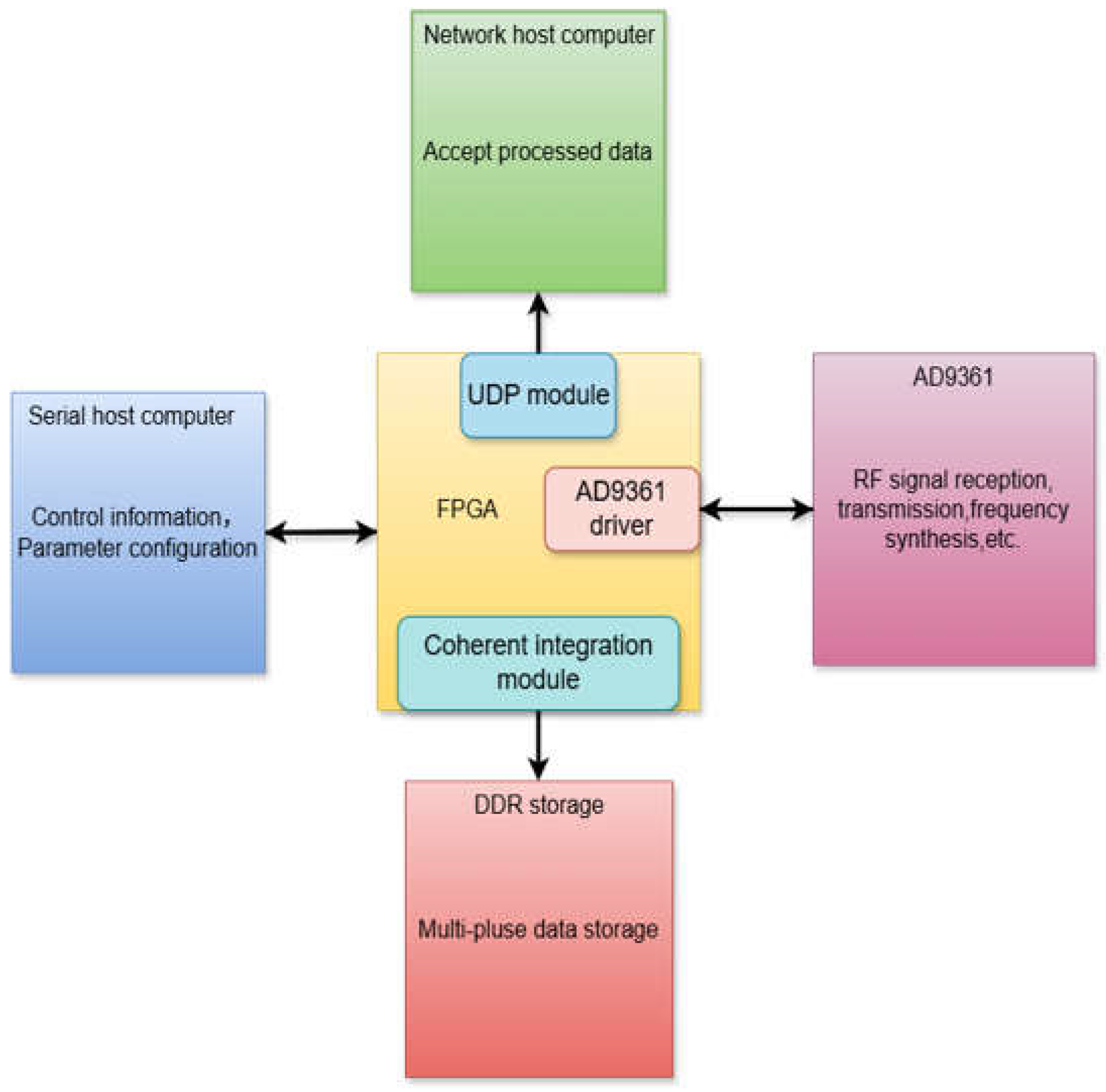
Figure 2.
Logical structure of the top layer of the system.
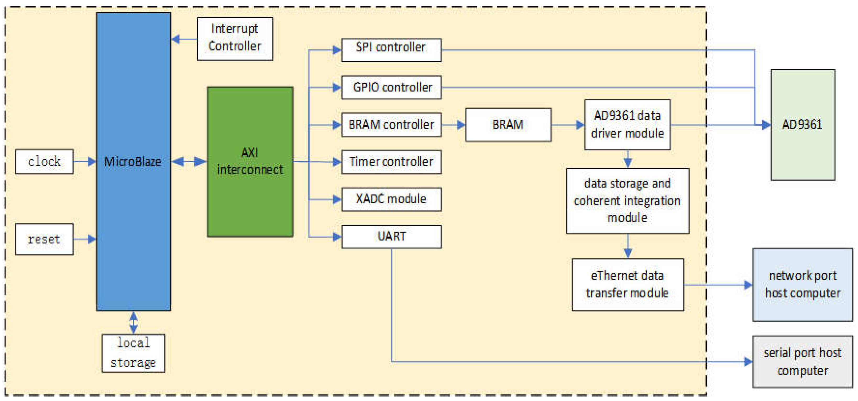
Figure 1.
AD9361 receive timing diagram.
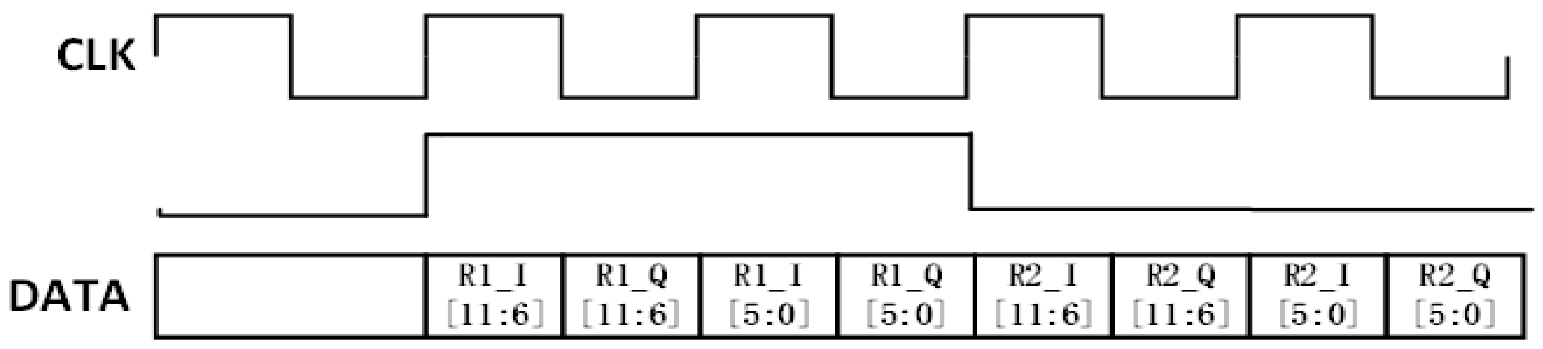
Figure 4.
AD9361 data reception processing block diagram.
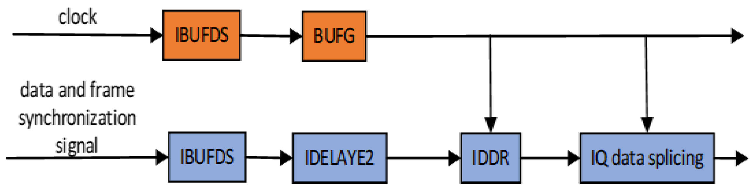
Figure 5.
Structure of data storage and coherent integration module.
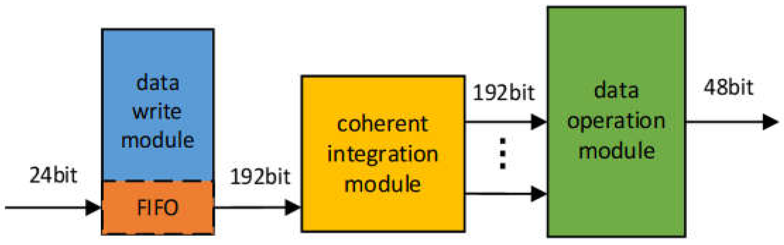
Figure 6.
Schematic diagram of data storage and output.
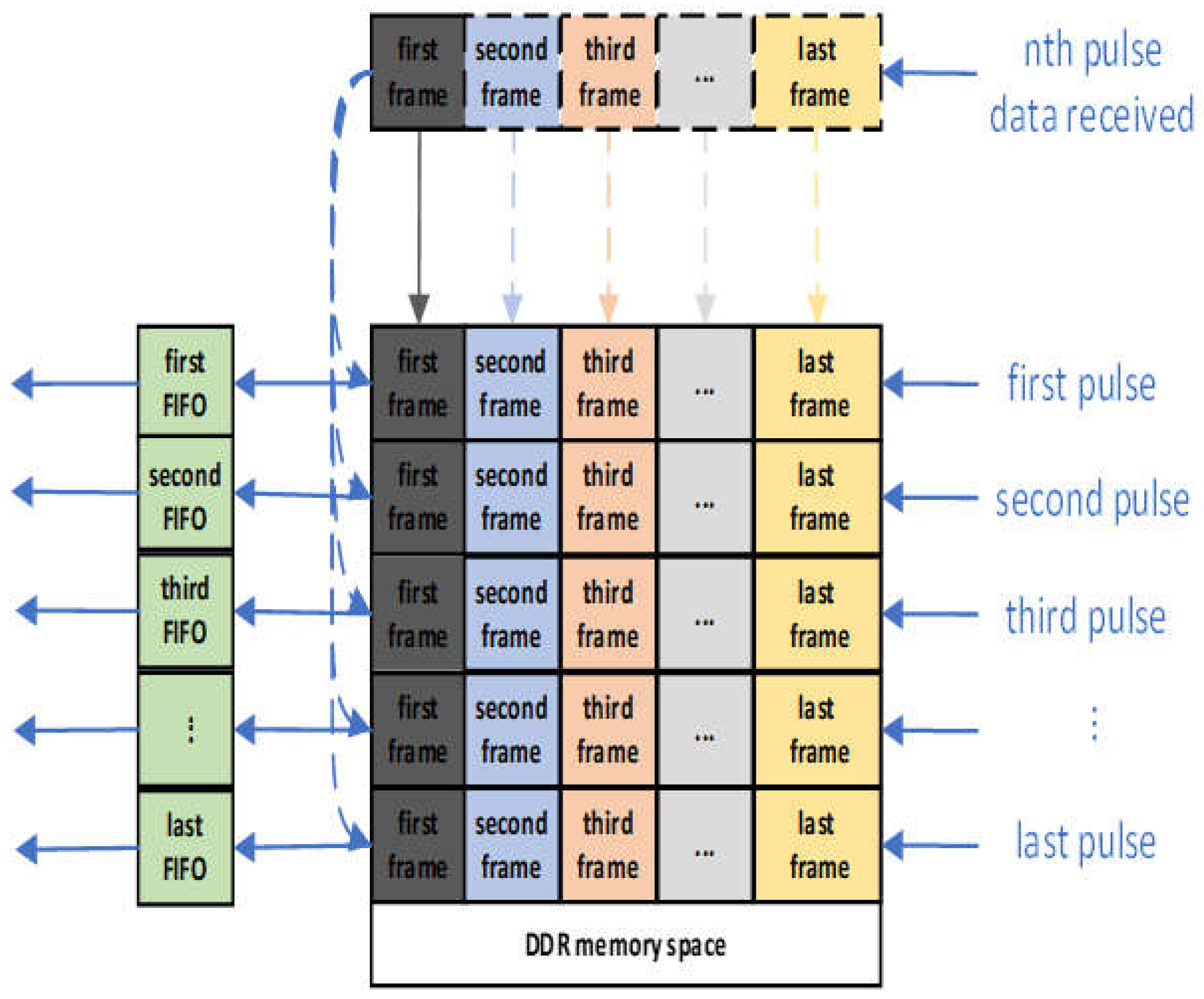
Figure 7.
Data operation diagram.
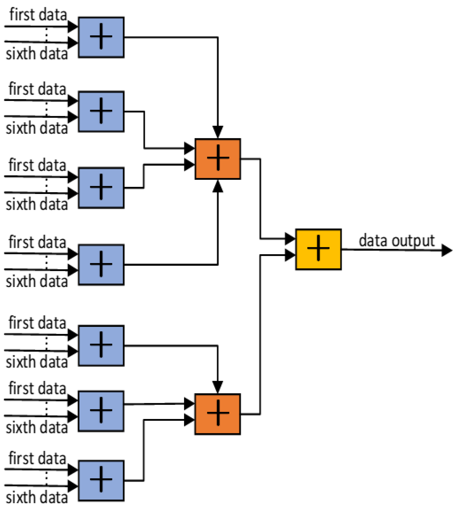
Figure 8.
UDP send FSM state diagram.
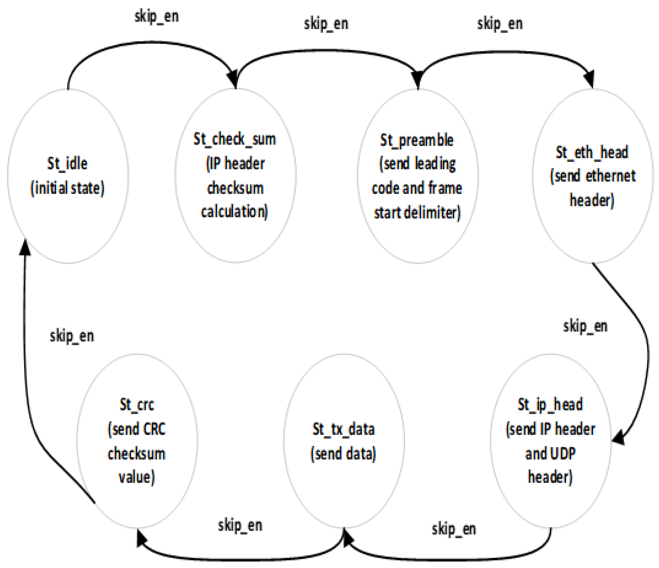
Figure 9.
Serial port host computer.
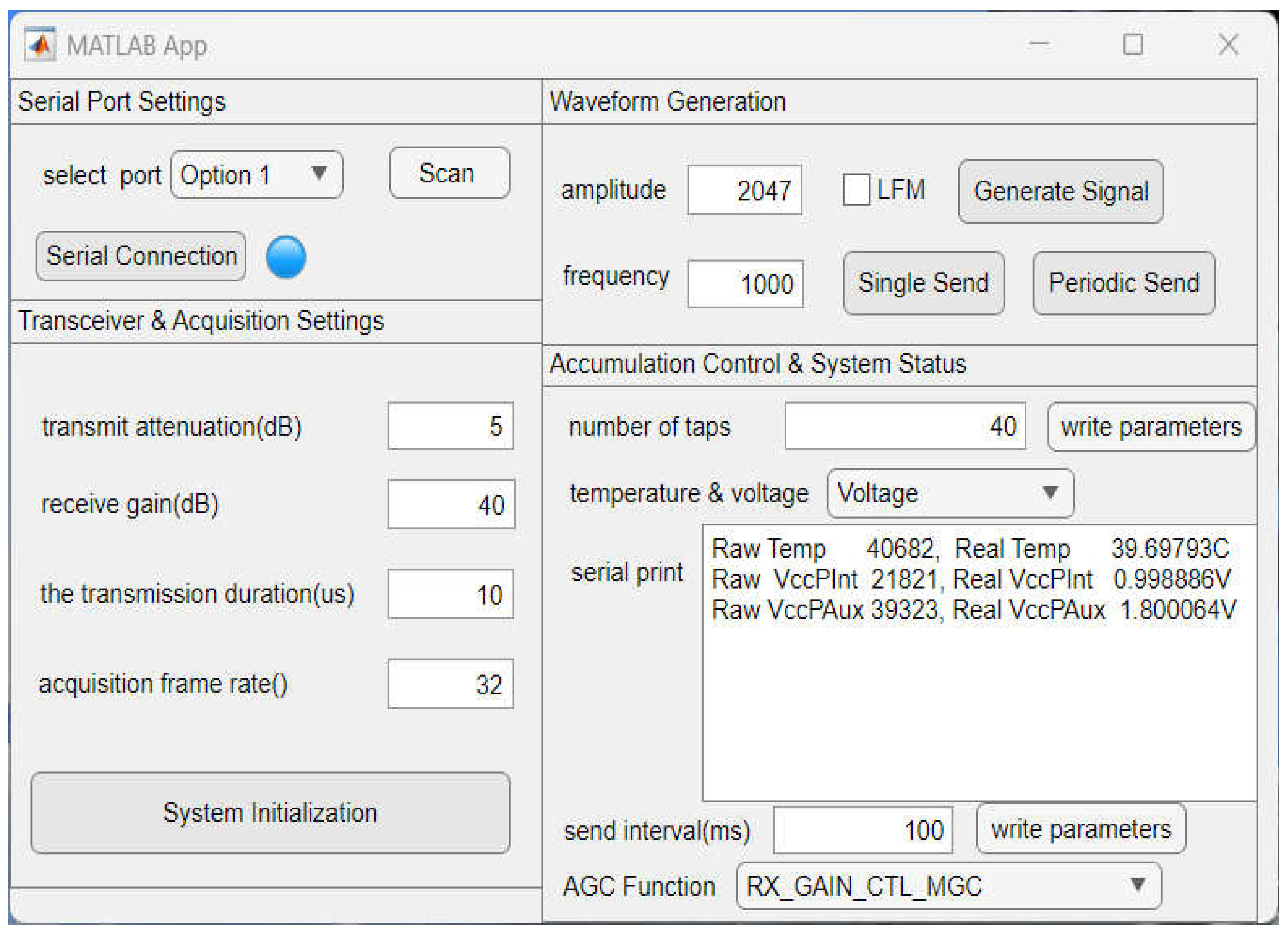
Figure 10.
Ethernet host computer.
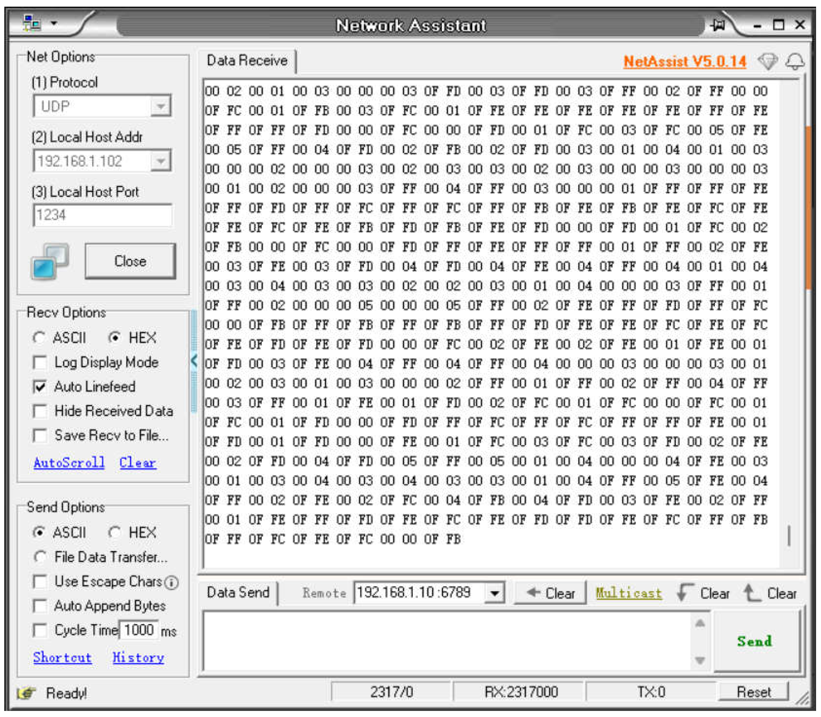
Figure 11.
Physical system test photo.
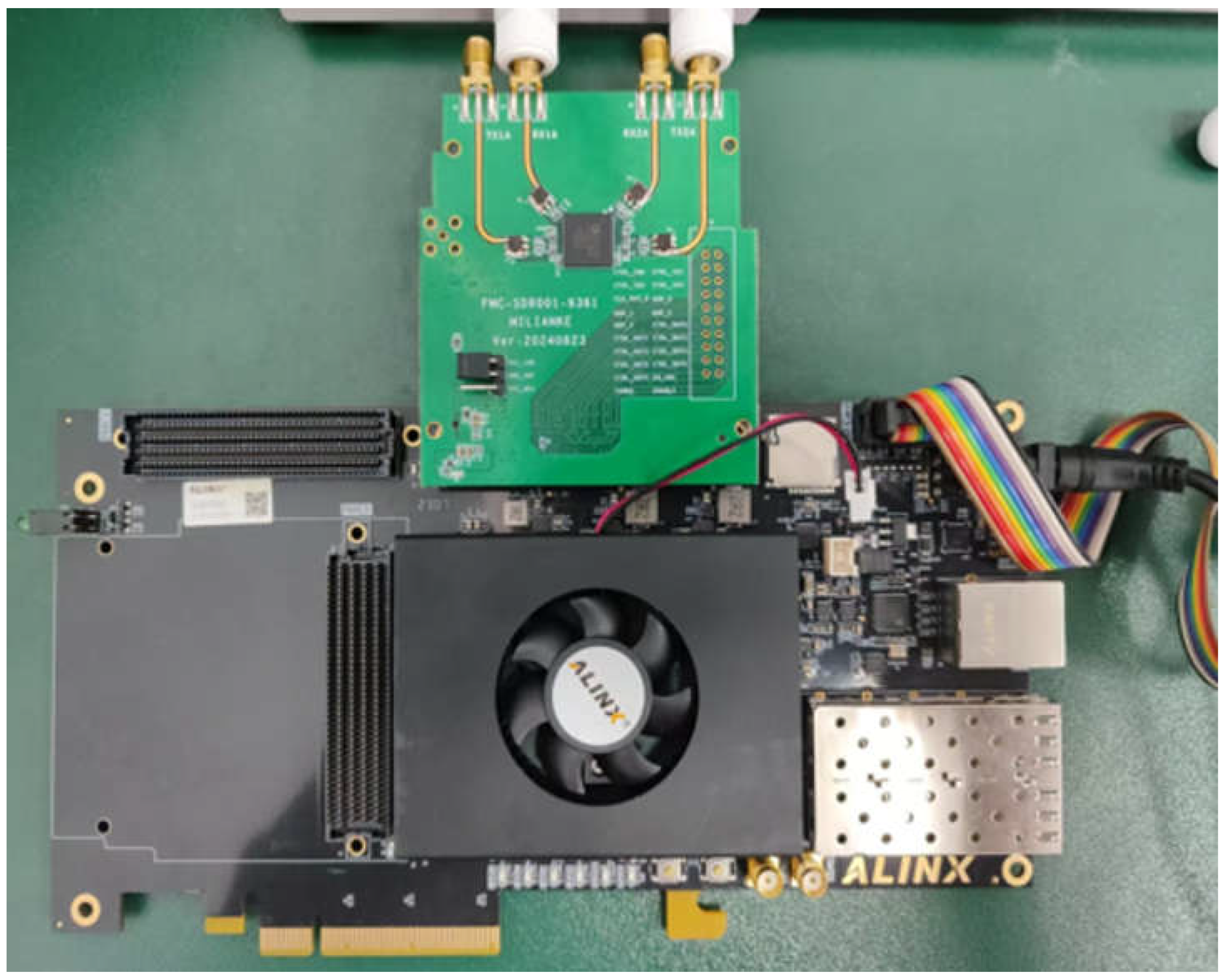
Figure 12.
Single-tone signal local loopback test.
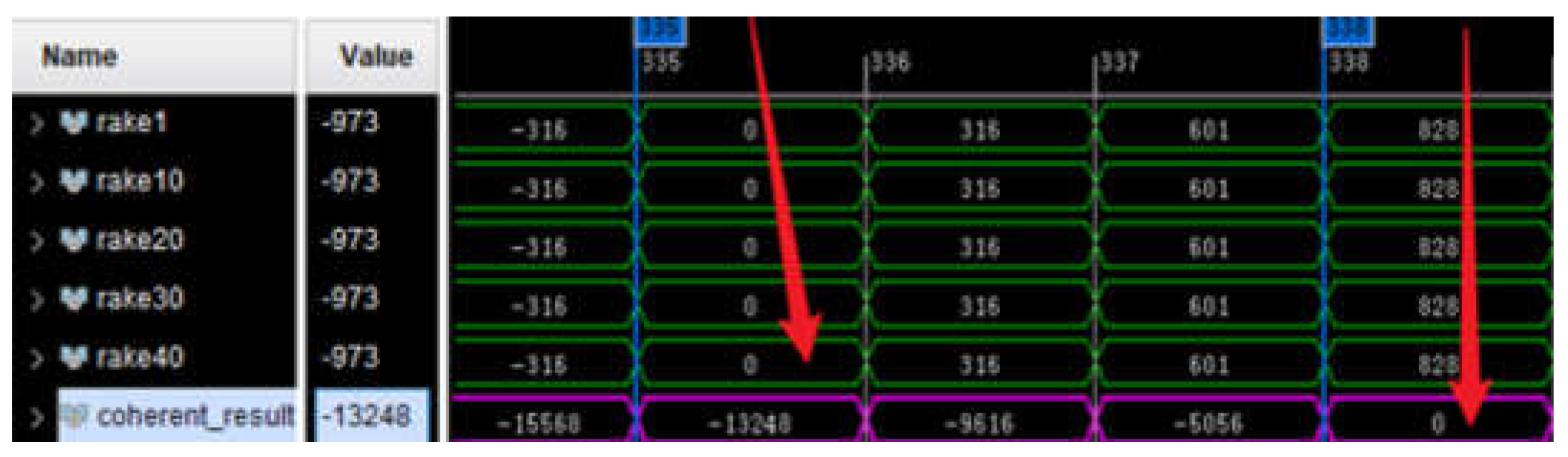
Figure 13.
Output results for different numbers of pulses.
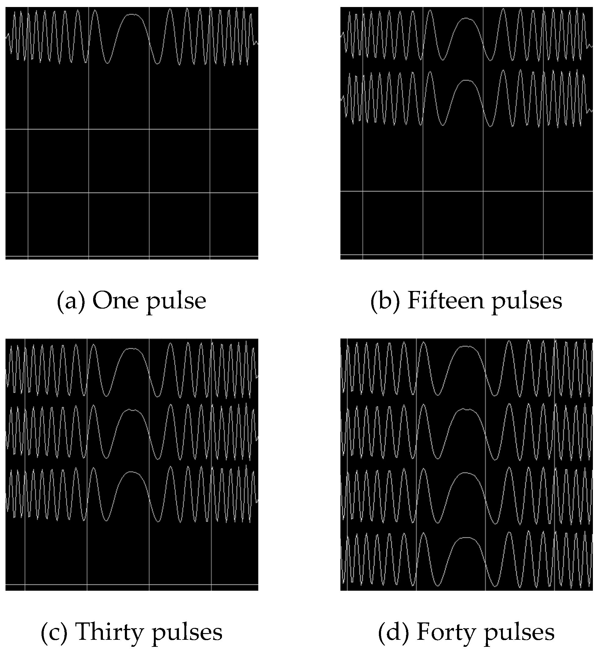
Figure 14.
Waveform of LFM signal with coherent integration.
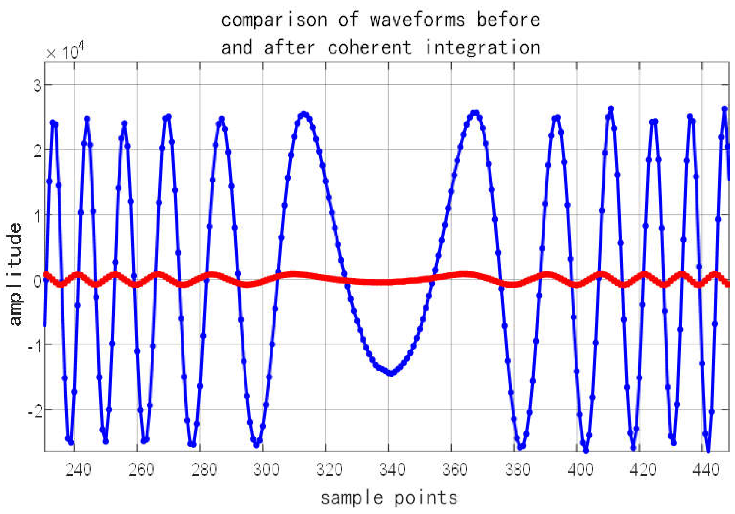

Table 1.
Test delay times.
| Number of pulses coherent integration /(pcs) | Number of pulse storage frames/(pcs) | Initial multi-pulse buffer time/(ms) | coherent integration data output delay/(us) |
| 20 | 100 | 34 | 24 |
| 20 | 1000 | 340 | 24 |
| 40 | 100 | 68 | 33 |
| 40 | 1000 | 680 | 33 |
Disclaimer/Publisher’s Note: The statements, opinions and data contained in all publications are solely those of the individual author(s) and contributor(s) and not of MDPI and/or the editor(s). MDPI and/or the editor(s) disclaim responsibility for any injury to people or property resulting from any ideas, methods, instructions or products referred to in the content. |
© 2025 by the authors. Licensee MDPI, Basel, Switzerland. This article is an open access article distributed under the terms and conditions of the Creative Commons Attribution (CC BY) license (http://creativecommons.org/licenses/by/4.0/).
Copyright: This open access article is published under a Creative Commons CC BY 4.0 license, which permit the free download, distribution, and reuse, provided that the author and preprint are cited in any reuse.


