
Submitted:
08 December 2025
Posted:
09 December 2025
You are already at the latest version
Abstract
Silicon multilayer thin films consisting of alternating amorphous SiOx (a-SiOx) and nanocrystalline silicon (nc-Si) layers were fabricated on p-type silicon substrates using a sol-gel spin-coating method. Boron-doped silicon powders, prepared through pro-longed grinding, were mixed with a TEOS–ethanol sol-gel solution, and two nc-Si layers embedded in a-SiOx were sequentially deposited. The as-grown films were an-nealed at 100–400 °C and characterized using Raman spectroscopy, GXRD, FTIR, SEM, Resistivity and UV spectroscopy to analyze their structural, chemical, optical, and electronic properties. Annealing progressively enhanced crystallinity and increased the < 111> and < 110> grain sizes to ~11 nm and ~12 nm, respectively. Films annealed at higher temperatures showed a minimum mobility of ~37.5 cm²/V·s, maximum resis-tivity of ~7.35 Ω·cm, and a decreasing optical bandgap. Enhanced nanocrystal growth, reduced defects, and improved structural ordering intensified the 520 cm⁻¹ Raman peak. The multilayer architecture further strengthened these effects by offering addi-tional nucleation sites, controlled nanocrystal confinement, defect-relaxing interfaces, improved phonon transport, and enhanced Si diffusion, resulting in superior crystal-line quality.
Keywords:
silicon
; thin film
; sol-gel
; silicon-dot and silicon oxide
1. Introduction
Multilayer silicon thin films have attracted much attention since they can be applied for many kinds of optoelectronic devices, such as the next generation of solar cells technology and light emitting devices [1]. The structural properties of nc-Si layers and the quality of buffer layers have a great impact on the device’s performance. For higher efficiency, high quality textured silicon thin films are needed. To obtain it, the analysis of grain size, structure and morphology of the thin layers are crucial. Efforts have been taken recently to fabricate high efficiency solar cells using improved amorphous and microcrystalline silicon [2,3,4,5,6,7]. The main challenge for the solar industry is to reduce the usage of materials and the deposition cost, and to increase the efficiency of photovoltaic devices. Silicon (Si) as an optically active layer appeared to be impossible to utilize properly because of its indirect band gap.
However, in recent years, nc-Si materials are showing many revolutions of photonic functions and the quantum confinement effect (QCE) of charge excitons in the silicon nanostructure is leading to a quasi-direct transition. In particular, the nc-Si band gap energy (Eg) can be elongated to shift down the valence states and to shifting up of the conduction states once the small nanometric size approaches the size of its Bohr exciton radius. The band gap modification due to the quantum confinement will be given in a simple effective mass approximation as follows: ∆Eg∝1/(m.a2 ) where m is an effective isotropic mass in the confinement direction, and a is a nanoparticle size.
Various conventional deposition techniques such as plasma enhanced chemical vapor deposition (PECVD)[8], RF magnetron sputtering [9], Ion implantation [10] and so on have been used to deposit nc-Si:H thin films which are compatible with the standard Si technology. However, it is very difficult in achieving concentrations high enough to obtain efficient optical properties. Many techniques mentioned above have been found to be expensive and time-consuming because of the production under high vacuum and/or annealing processes. A sol-gel method is quite inexpensive and easy to fabricate such Si nanocrystals embedded into its dielectric matrix. The sol-gel method by centrifugal processing has been recommended as a technique to be achieved in this objective [11]. The sol-gel was used as a viscous medium through Si crystallites settle. Nevertheless, centrifugal processing might produce bulk material which has such a functional constraint for thin film optoelectronic devices.
In this study, four multilayer nc-Si/Si thin-film samples were prepared using an identical sol–gel spin-coating process, followed by annealing at 100 °C, 200 °C, 300 °C, and 400 °C. The resulting silicon nanostructures consisted of nano-Si powders dispersed within a continuous SiO2 matrix. Boron-doped p-type (100) Si wafers were finely ground to serve as the nano-Si powder precursor. A sol–gel–derived SiO2 buffer layer, synthesized using the buffer solution described below, served as a critical component of the multilayer architecture.
Compositional analysis and the chemical bonding environment of boron were examined using FTIR spectroscopy. The structural, optical, and electronic properties of the ML nc-Si/Si thin films were characterized using Raman spectroscopy, glancing-incidence XRD, ellipsometry, four-point-probe measurements, SEM, and UV spectroscopy.
2. Materials and Methods
2.1. Substrates Preparation
Multilayer nanocrystalline silicon (ML nc-Si/Si) thin films were deposited on boron-doped p-type silicon substrates. Prior to deposition, the substrates were ultrasonically cleaned for 15 minutes each in acetone, ethanol, and deionized (DI) water.
2.2. Nano-Si Powders Preparation
The nano-Si powders were produced from (100) p-type monocrystalline Si wafers by a prolonged grinding process lasting 4–10 hours. The wafers contained boron impurities corresponding to a resistivity of 1–20 Ω·cm. The resulting Si powders were then mixed with absolute ethanol and passed through a 20 µm pore-size sieve for filtration.
2.3. Preparation of SiO2 Buffer Layer
Tetraethylorthosilicate, Si(OC2H5)4 (TEOS, 98% Fluka) and ethanol absolute, (C2H5OH, 99% BDH) (EtOH)) were used in this experiment, as a silicon-oxide precursor. In the fabrication of Si oxide buffer layer, the dielectric sol-gel (buffer solution) was first prepared as follows: 1 mole of TEOS and 2 moles of EtOH were mixed and then stirred for 15 min at the room temperature. Cetyl Trimethyl Ammonium Bromide, C19H42BrN (CTAB, 99% Sigma Aldrich) was used as surfactant. In addition, 0.0013M CTAB and 0.1M HCl catalysts in water were subsequently added dropwise to the solution until the water to TEOS molar ratio of 2. The condensation of TEOS at about pH = 2 was controlled by adding HCl catalyst. The proper solutions were then stirred at room temperature for 60 minutes. To obtain the suspension uniformity, sol-suspension was prepared from the mixture of nano-scaled Si powders (0.10 g) with TEOS (buffer solution) of 5ml under a magnetic stirrer for 30 min [12]. The conditions of substrate cleaning and film deposition are summarized in Table 1 and Table 2.
[Si(OC2H5)4 + C2H5OH] + [C19H42BrN + HCl] → SiO2 Buffer Solution
2.4. Synthesis of nc-Si/Si Thin Films Layers
Figure 1 shows the spin-coating setup used in this experiment. Nitrogen (N2) gas cylinder as back pressure is connected to the liquid dispenser. Sol-gel liquid holder is also connected to the liquid dispenser with a stand just above the spin coater disk. Adjusting the back pressure, the amount of precursor liquid (0.1 ml) can be disseminated on the mounted p-type Si (100) substrate in the spin coater.
After aging of the gel for 8-day, 0.2 ml of the prepared TEOS gel as a si-oxide precursor was spun at 11,800 rpm for 10 s on silicon substrate. The acquired Si-oxide is an important buffer layer to have a good coherence between its surface and the sol-suspension for the next step. To inhibit the crack of the buffer layer structure, the first Si-oxide film was suitably dried for 2 hours on a hot plate in air ambient at 50oC. Afterward, 0.2ml of sol-suspension was released from the sol-gel holder located just above the spin coater on the dried oxide buffer layer and nc-Si thin film deposition was performed by spinning the coater for 10 s with same rpm of 11,800 as above. By repeating the above proper sequence processes, two layers of nc-Si thin films were prepared in a continuous oxide dielectric phase in this work.
2.5. Stoichiometry of SiOx Buffer Layer
The stoichiometry of as-deposited SiOx was estimated by 2 (SiO2) from shifts of the asymmetric Si-O-Si stretching peak with adjacent O-atoms in the IR absorption spectra. The change in chemical bonding state of Si oxide film was also analyzed by using Fourier transform infrared spectroscopy, FT-IR (Perkin-Elmer System 2000) with a wavenumber resolution of 2 cm−1 as the following equation:
where [ψ] is a position of peak frequency (cm−1) and x is stoichiometry of SiOx film [12].
[ψ] = 978.72 + 30.63x
3. Results
3.1. Raman Scattering
The transition of thin film structure and the degree of MLnc-Si/Si crystallinity have been investigated by Raman scattering measurements. The Raman spectra of the films were recorded using a portable iRaman (B&W TeK) with the argon ion laser having an excitation wavelength of 514 nm was used and the power was less than 5 mW.
Figure 2 shows (a) the Raman spectra of as-synthesized silicon (p-type, B-doped, 1-20 Ω-cm) powders and (b) the Raman spectra of MLnc-Si/Si thin films as a function of annealing temperatures. Sharp peak centered at ~519.23 cm−1 is clearly indicating the crystalline phase (Figure 2a).
Figure 2b shows the Raman spectra of ML nc-Si/Si thin films as a function of annealing temperature. It is observed that all films have shown a strong narrow peak at 520 cm-1 and the Raman intensity is gradually enhanced with increasing the annealing temperature which is indicating the enhancement of crystallization.
Figure 3 shows the crystallite size and Full Width Half Maximum (FWHM) as a function of annealing temperature. With increasing annealing temperature, crystallite size estimated using Eq. 3, goes up and has the maximum of 10.98 nm at 400oC (Fig.3). On the other hand, FWHM showed the opposite relationship. It seems that the increment of annealing temperature is helpful for promoting crystallization. Results indicate that with increasing the annealing temperature, the crystallites size of formed MLnc-Si is increased and becomes more ordered which may be related to reduce the strain in the films. The Raman crystallites size was estimated from FWHM using the equation as follows [13]
where A = 47.41 cm−1, γ = 1.44, β = 0.543 nm), L is silicon dot diameter, and ∆ω is the FWHM.
Δω = - A(β/L)^γ
With increasing annealing temperature, the films show enhanced crystallinity, reduced defects, enlarged and better-ordered nanocrystals, and improved Raman scattering efficiency, resulting in a stronger 520 cm−1 Raman peak. The multilayer architecture amplifies the annealing effects by providing more nucleation sites for faster crystallization, a confined geometry for controlled nanocrystal growth, interfaces that relax defects, improved phonon transport that strengthens the 520 cm−1 Raman peak, and enhanced Si diffusion that promotes better crystal ordering.
3.2. X-Ray Diffraction (XRD)
The structural properties were investigated using an XRD instrument (SIEMENS D5000 X-ray diffractometer, λ = 1.54 Å). The XRD spectra were recorded in the 2θ range from 20o to 80o at a fixed grazing angle of 5o and a scan rate of 0.02o/s. In the present study, any difference in the film thickness was corrected using the X-ray absorption coefficient for Si. Thus, the XRD intensities observed for different films can be compared. The average crystallite size, [δ], was estimated from the width of the XRD spectra using Scherrer’s formula as follows:
where k, λ, β and θ are a constant, the wavelength of X-ray (1.54 Å), the full width at half maximum (FWHM) and Bragg angle of the diffraction peak respectively.
[δ] = kλ/βcosθ
Figure 4 shows the Glancing angle XRD (GXRD) spectra of MLnc-Si/Si thin films as a function of annealing temperature. Strong diffraction peaks of (111) and (220) planes were observed for all the samples (Fig. 4). Films show a (111) preferential orientation. An increase in the relative intensity of the (111) and (220) XRD spectra were found as a function of annealing temperature corresponds well with an increase in the intensity of 520 cm-1 component (crystalline phase) in Raman spectra.
Figure 5 shows the (111) and (110) XRD grain sizes ([δ]) as a function of annealing temperature. Both (111) and (110), [δ] were found to be increased with increasing annealing temperature. Maximum [δ] were found to be <111> ~ 12 nm and (110) ~ 11 nm at 400oC. XRD results are well consistent with Raman results.
Results show both Raman and XRD confirm the same structural evolution: the multilayer design enhances crystallization and reduces disorder during annealing.
3.3. Fourier Transform Infra-Red (FT-IR)
Figure 6 shows the IR absorption spectra over the range of 400-4000 cm-1 for films deposited with different annealing temperatures. The IR absorption was measured by a Thermo- Scientific, Nicolet iS10 FTIR spectroscopy with the wavenumber range of 400 to 4,000 cm-1 and resolution of 2 cm-1. The spectra at 747.97 cm-1, 902.49 cm-1 and 1541.66 cm-1 are assigned to Si-O Rocking, Si-O bending, Si-O stretching and adjacent O-atom out of phase absorption bands, respectively. These bands are attributed to the in-phase motion of the oxygen atoms [14].
In multilayer nc-Si/Si films, the repeated Si/SiOₓ interfaces create well-defined Si–O–Si structural units, and these interfaces enhance the coordinated (in-phase) vibrational motions of oxygen atoms. As a result, the characteristic Si–O rocking, bending, and stretching bands become more pronounced in the IR spectra, because the multilayer architecture provides more ordered and repeated Si–O bonding environments that strengthen these vibrational modes.
3.4. Scanning Electron Microscope (SEM)
The topological images were taken by scanning electron microscopy (SEM, 1450VP, Phenom Pure). Figure 7 shows the SEM micro graphs of ML nc-Si/Si thin films as a function of annealing temperature, (a) Cross-sectional view of nc-Si top-layer and (b) Topographic view. It is a branch of microscopy that produces images of a sample by scanning the surface with a focused beam of electrons. The electrons interact with atoms in the sample, producing various signals that contain information about both the sample’s surface morphology, cross-sectional information and the composition as well. As shown in Figure 7a, average film thickness was estimated ~1 micrometer. As shown in Figure 7b, ununiformed larger island-type of micro-structured was observed for the film deposited at 100oC. However, at 400oC, uniformed grains distributions were observed, which also showing the crack-free uniform surface with the highest crystallinity as shown above [15].
3.5. Optical Measurement and Band Gap Energy
The optical band gap energy of ML nc-Si/Si thin film is calculated by Tauc’s equation as below:
where hν is photon energy and n is equal to ½ and 2 respectively. The linear variation of (αhν) 2 vs. hν at absorption edge. The Extrapolating the straight-line portion of the plot (αhν)2 versus hν for zero absorption coefficient values gives the optical band gap (Eg). Figure 8 shows the optical transmittance spectra of ML nc-Si/Si thin films as a function of annealing temperature. The transmittance spectrum revealed a high transparency above 90% in the near-infrared region providing a potential application for infrared optoelectronic devices.
(αhν)=A(hν-Eg)n
However, the transmittance was improved in the visible region with the wavelength less than 650 nm generally due to the optical absorption characteristics of the ML nc-Si/Si thin films which are near their optical band gap region as the annealing temperature increased due to the lower band gap energy.
Figure 9 shows the optical band gap energy (Eg) of ML nc-Si/Si as a function of annealing temperature. Optical band gap energy decreased with increasing the annealing temperature having the lowest value, Eg = 1.3 eV at 400oC. The decrease in optical band gap energy with increasing annealing temperature can be attributed to structural relaxation and increased crystallinity within the nc-Si films. At higher annealing temperatures, nanocrystalline grains tend to grow, and the degree of disorder or amorphous fractions within the film are reduced. As the crystallite size increases, the quantum confinement effect becomes weaker.
In nanocrystalline or partially amorphous silicon, stronger confinement in smaller grains produces a wider band gap. When annealing promotes grain growth and reduces disorder, the electronic states become more delocalized, narrowing the band gap. This results in the lowest band gap value (Eg ≈ 1.3 eV at 400 °C).
Additionally, high-temperature annealing can reduce defect-related localized states within the band gap. The reduction of these defect states shifts the optical absorption edge toward lower energies, further contributing to a decreased optical band gap.
3.6. Ellipsometry
Thickness of the films was obtained by using an ellipsometer (Rudolph Research, Ellipsometer Auto EL-III) with a wavelength of 632.8 nm. Figure 10 shows the influence of annealing temperature of the ML nc-Si/Si thin film on the thickness and refractive index values. By increasing the annealing temperature, the average value of the refractive index exhibits a slight increase from 3.32-3.59. It might contribute to start of pore removal and densification as a function of annealing temperature. Moreover, the film thickness gradually shrinks from 950 nm to 689 nm.
It is mainly due to the shrinkage of the gels during drying, and it is forced by capillary pressure of the small pore liquid [16]. Using annealing temperature, the surface tension between liquid and vapor plays a very important role. Therefore, the less shrinkage of the film annealed at 400oC can lead to the less crack or crack free. With increasing the annealing temperature, the thickness was found to be decreased because of more gel viscosity. Moreover, thickness and refractive index were showing the opposite relationship to each other due to that EtOH as a solvent evaporates, causing shrinkage of the gel network.
3.7. Electrical Measurement
The resistivity [μ] of ML nc-Si/Si thin films was measured using four-point probes by the following equation:
where v and I are voltage and current respectively.
[μ] = π/ln2 V/I
Figure 11 shows the variation of hall mobility and the resistivity of nc-Si thin films as a function of annealing temperature. Mobility and resistivity show opposite relationships to each other having the minimum mobility of ~37.5 cm2/v.s and the maximum resistivity of ~7.35 Ω-cm at higher annealing temperature, respectively.
The observed opposite trends of Hall mobility and resistivity with increasing annealing temperature can be explained by changes in the microstructure and defect density of the nc-Si thin films. As the annealing temperature increases, structural disorder, grain boundary defects, or impurity scattering may become more pronounced. These defects act as scattering centers that hinder charge carrier movement, resulting in reduced mobility (down to ~37.5 cm2/V·s at the highest annealing temperature).
At the same time, an increase in defect density or the formation of insulating phases can decrease effective carrier concentration. Since resistivity (ρ) is inversely related to both carrier concentration (n) and mobility (μ) through the relation ρ = 1/(n·q·μ), a reduction in either parameter leads to higher resistivity. Consequently, the films exhibit maximum resistivity (~7.35 Ω·cm) at higher annealing temperatures.
Thus, the opposite behavior of mobility and resistivity arises because increased thermal treatment degrades charge transport pathways by introducing or enlarging defect-related barriers within the nanocrystalline silicon network.
4. Discussion
Multilayer nanocrystalline silicon (nc-Si/Si) thin films were fabricated on crystalline silicon substrates using a spin-coating approach, followed by thermal annealing at progressively higher temperatures. The annealing treatment played a central role in governing the structural, electrical, and optical properties of the films. As the annealing temperature increased, the films exhibited a clear enhancement in crystallinity, reflected by the systematic growth of nanocrystalline domains and improved orientation. X-ray diffraction analysis revealed that the average grain sizes associated with the <111> and <110> orientations were approximately 11 nm and 12 nm, respectively, indicating the formation of relatively uniform and well-developed nanocrystals. The increase in grain size at elevated annealing temperatures suggests enhanced atomic mobility and more complete crystallization within the multilayer structure.
Electrical characterization further demonstrated the strong influence of annealing. At the highest annealing temperatures, the films displayed a minimum charge-carrier mobility of ~37.5 cm2/V·s accompanied by a maximum resistivity of ~7.35 Ω·cm. This inverse relationship between mobility and resistivity is consistent with changes in microstructure: while improved crystallinity generally favors charge transport, the presence of grain boundaries, defect states, and possible depletion regions can counteract mobility gains. The observed trends imply that although crystallization is enhanced at higher temperatures, scattering at enlarged grain boundaries or residual defects may still limit mobility.
Optical measurements showed a continuous decrease in bandgap energy with increasing annealing temperature, reaching its lowest value of approximately 1.3 eV at 400 °C. This reduction in optical bandgap aligns with the transition from a more amorphous to a more crystalline state, where the weakening of quantum confinement and the reduction of localized defect states both contribute to bandgap narrowing. The evolution of the bandgap, therefore, supports the structural findings and confirms the enhancement of long-range order in the material.
Raman spectroscopy provided additional evidence of structural improvement. With higher annealing temperatures, the intensity of the characteristic crystalline Si Raman peak at ~520 cm−1 increased significantly. This enhancement is attributed to reduced disorder, improved phonon coherence, and the enlargement of crystalline regions. The strengthened 520 cm−1 peak confirms that the films developed higher crystallinity and lower defect density as annealing progressed.
The multilayer architecture of the films further amplifies these annealing-induced improvements. The repeated stacking of thin layers creates abundant nucleation sites that promote rapid crystallization during thermal treatment. The confined geometry of each layer restricts crystal growth in a controlled manner, promoting uniform nanocrystal sizes and minimizing the formation of extended defects. Additionally, the interfaces between layers help relieve structural strain and reduce defect densities, contributing to improved microstructural quality. Enhanced phonon transport across well-ordered multilayers also increases Raman scattering efficiency, giving rise to the more intense 520 cm−1 Raman signature. Moreover, the multilayer design facilitates interlayer silicon diffusion during annealing, which further smooths structural discontinuities and promotes the formation of highly oriented nanocrystals.
Overall, the results collectively demonstrate that thermal annealing-combined with the advantages of a multilayer configuration-significantly improves crystallinity, optical properties, and structural quality in nc-Si thin films. These improvements highlight the effectiveness of multilayer spin-coated architectures for tailoring the structural and functional properties of silicon-based nanomaterials.
5. Conclusions
Multilayer nanocrystalline silicon thin films were deposited on silicon substrates using a spin-coating technique and subsequently annealed at various temperatures. The crystallinity and grain size of the films increased progressively with higher annealing temperatures. The average grain sizes for the <111> and <110> orientations were approximately 11 nm and 12 nm, respectively. At elevated annealing temperatures, the films exhibited a minimum mobility of ~37.5 cm2/V·s and a maximum resistivity of ~7.35 Ω·cm. The optical bandgap decreased with increasing annealing temperature, consistent with enhanced structural ordering. Higher annealing temperatures resulted in improved crystallinity, reduced defect density, enlarged and better-oriented nanocrystals, and enhanced Raman scattering efficiency, leading to a more intense 520 cm−1 Raman peak. The multilayer architecture further amplifies these annealing effects by providing additional nucleation sites for rapid crystallization, a confined geometry for controlled nanocrystal growth, interfaces that help relax structural defects, improved phonon transport that strengthens the 520 cm−1 Raman mode and facilitated silicon diffusion that promotes superior crystal ordering.
| ML | Multilayer |
| QCE | Quantum confinement effect |
| XRD | X-Ray Diffraction |
| FT-IR | Fourier transform infrared |
Author Contributions
This research was conducted by Dr. Moniruzzaman Syed and his students—Joe Mvula, Brittany Anderson, Princess Benson, Brittany Cook, Eddie Hollins, and Patrick Taylor—in collaboration with Dr. Ismat Shah Syed at the University of Delaware. Sample preparation was carried out at LeMoyne-Owen College, while Raman, XRD, and SEM measurements were performed in Dr. Shah’s laboratory. The LeMoyne-Owen College students completed the data analysis and contributed to manuscript preparation under the supervision of Dr. Syed.
Funding
Financial support from the National Science Foundation (Grant No. HRD-1332459) is gratefully acknowledged for making this research possible.
Acknowledgments
The authors would like to thank Dr. Sherry Painter, Division Chair at LeMoyne-Owen College, for her support throughout this work. Special appreciation is extended to Dr. Delphia Harris, Professor of Chemistry at LeMoyne-Owen College, for her valuable suggestions. The authors also acknowledge Dr. Sanjay Mishra of the Department of Physics and Materials Science at the University of Memphis for providing access to characterization facilities.
Conflicts of Interest
The authors declare no conflicts of interest. The funders had no role in the design of the study; in the collection, analyses, or interpretation of data; in the writing of the manuscript; or in the decision to publish the results.
The following abbreviations are used in this manuscript:
References
- Huh, C.; Kim, T.Y.; Ahn, C.G.; Kim, B. Y. Appl. Phys. Lett. 2015, 106, 211103. [CrossRef]
- Becker, C; Amkreutz, D; Sontheimer, T; Preidel, V; Lockau, D; et al. Solar Energy Mater. Solar Cells 2013, 119, 112–123. [Google Scholar] [CrossRef]
- Cui, H; Campbell, PR; Green, MA. Energy Procedia 2013, 33, 118–128. [CrossRef]
- Cannella, G; Principato, F; Foti, M; Gerardi, C; Lombardo, S. Comparison between textured SnO2:F and Mo contacts with the p-type layer in p-i-n hydrogenate amorphous silicon solar cells by forward bias impedance analysis. Solar Energy 2013, 88, 175–181. [Google Scholar] [CrossRef]
- Wen, X; Zeng, X; Liao, W; Lei, Q; Yin, S. Solar Energy 2013, 96, 168–176. [CrossRef]
- Hussain, SQ; Oh, WK; Ahn, S; Le, AHT; Kim, S; et al. Vacuum 2014, 101, 18–21. [CrossRef]
- Campa, A; Isabella, O; van Erven, R; Peeters, P; Borg, H; et al. Prog. Photovolt. Res. Appl 2010, 18, 160–167. [Google Scholar]
- M. Pe´ralvarez, J.; Barreto, J.; Carreras, A.; Morales, D.N.; Urrios, Y.; Lebour; Dom`ınguez, C.; Garrido, B. Si-nanocrystal-based LEDs fabricated by ion implantation and plasma-enhanced chemical vapor deposition. Nanotechnology 2009, 20, 405201. [Google Scholar] [CrossRef] [PubMed]
- Iacona, F.; Bongiorno, C.; Spinella, C.; Boninelli, S.; Priolo, F. Formation and evolution of lumi-nescent Si nano clusters produced by thermal an-nealing of SiOx films. Journal of Applied Physics 2004, 95, 3723–3732. [Google Scholar] [CrossRef]
- Fauchet, P.M.; Ruan, J.; Chen, H.; Pavesi, L.; Dal Negro, L.; Cazzaneli, M.; Elliman, R.G.; Smith, N.; Samoc, M.; Luther-Davies, B. Optical gain in different silicon nanocrystal systems. Optical Materials 2005, 27, 745–749. [Google Scholar] [CrossRef]
- Duval, D.J.; McCoy, B.J.; Risbud, S.H.; Munir, Z.A. Size selected silicon particles in sol-gel glass by centrifugal processing. Journal of Applied Physics 1998, 83, 2301–2307. [Google Scholar] [CrossRef]
- Syed, Moniruzzaman; Anderson, Brittany; Mvula, Joe; Hamada, Yahia; Syed, Muhtadyuzzaman; Prasad Poudel, Tej. Effects of SiOx Aging Time on Nano Crystalline Silicon Thin Film for Optoelectronic Devices using Sol-Gel Method. International Journal of Scientific Research and Engineering Development 2019, Vol. 2(Issue 4). [Google Scholar]
- Zi, J.; Falter, H. Bscher. C.; Ludwig, W.; Zhang, K.; Xie, X. Raman shifts in Si nanocrystals. Applied Physical Letters 1996, 69, pp.200. [Google Scholar] [CrossRef]
- Pai, P. G.; Chao, S.S.; Takagi, Y.; Lucovski, G.J. Vac. Sci. Technol. 1986, A4, 689. [CrossRef]
- Mario, F.; Heinig, Dipanwita Chatterjee; Antonius; van Helvoort, T.J.; Wagner, Jakob Birkedal; Kadkhodazadeh, Shima; Ånes, Håkon Wiik; Niessen, Frank; Fanta, Alice Bastos da Silva. High resolution crystal orientation mapping of ultrathin films in SEM and TEM. Materials Characterization 2022, 189, pp. 111931. [Google Scholar] [CrossRef]
- Chen, Yuanhao; Sun, Dandan; Tang, Xiufeng; Zhang, Jiong. Effects of annealing temperature and time on the crystalline structure and electrochromic performance of WO3 thin films. Journal of Materials Science: Materials Electronics 2025, 36, pp. 1706. [Google Scholar] [CrossRef]
Figure 1.
(a) Schematic diagram of the Spin coater set up and (b) Cross-sectional diagram of MLnc-Si/Si thin film growth.
Figure 1.
(a) Schematic diagram of the Spin coater set up and (b) Cross-sectional diagram of MLnc-Si/Si thin film growth.
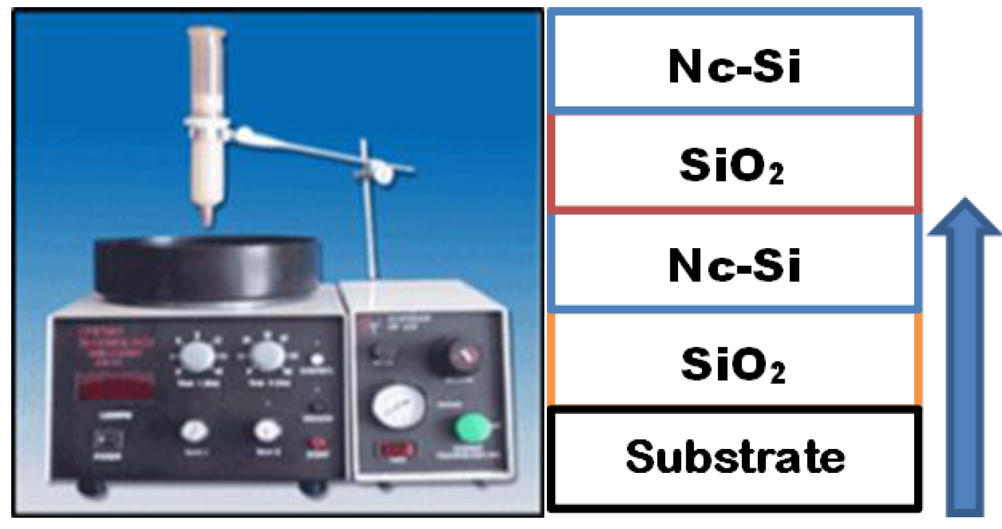
Figure 2.
(a) Under long grinding process, nc-Si powder was produced and (b) Raman spectra of MLnc-Si/Si thin films as a function of annealing temperature.
Figure 2.
(a) Under long grinding process, nc-Si powder was produced and (b) Raman spectra of MLnc-Si/Si thin films as a function of annealing temperature.
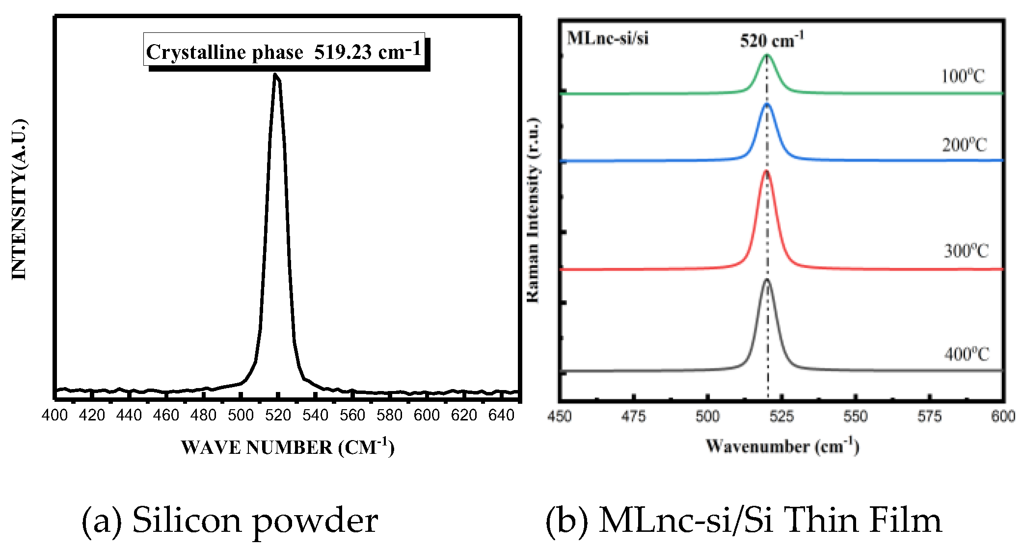
Figure 3.
shows the crystallite size and FWHM as a function of annealing temperature from Raman peaks.
Figure 3.
shows the crystallite size and FWHM as a function of annealing temperature from Raman peaks.
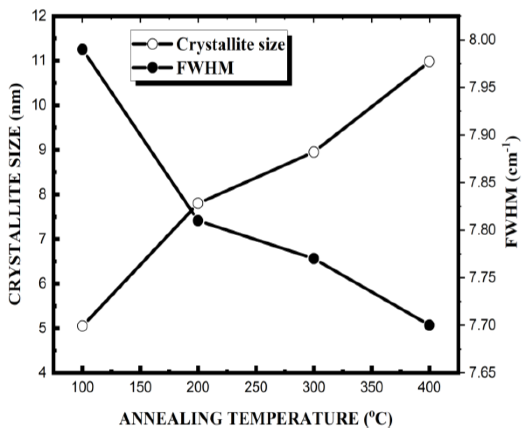
Figure 4.
Glancing angle X-ray diffraction patterns of ML nc-Si/Si as a function of annealing temperature.
Figure 4.
Glancing angle X-ray diffraction patterns of ML nc-Si/Si as a function of annealing temperature.
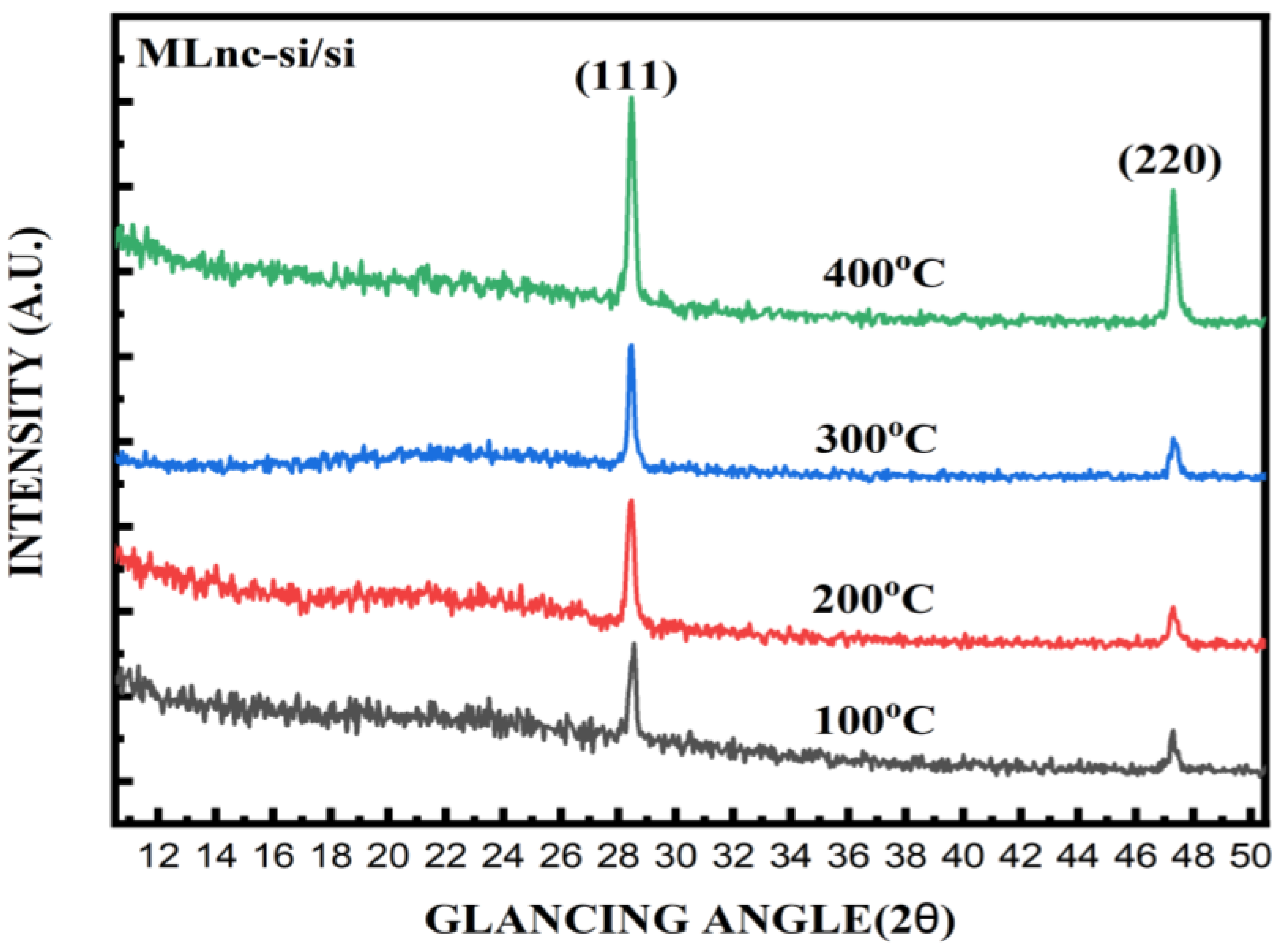
Figure 5.
GXRD Grain sizes of ML nc-Si/Si as a function of annealing temperature.
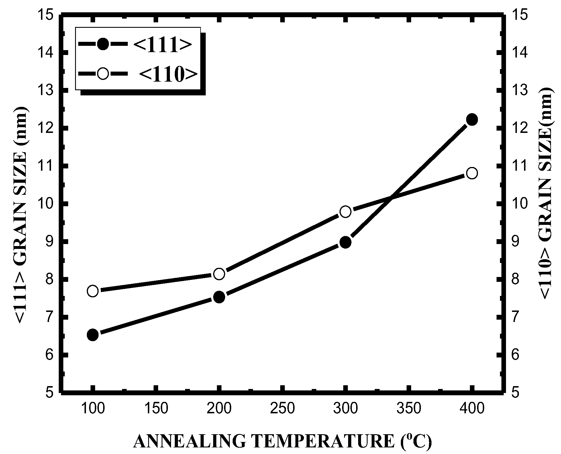
Figure 6.
FT/IR transmittance spectra of ML nc-Si/Si thin film as a function of annealing temperature.
Figure 6.
FT/IR transmittance spectra of ML nc-Si/Si thin film as a function of annealing temperature.
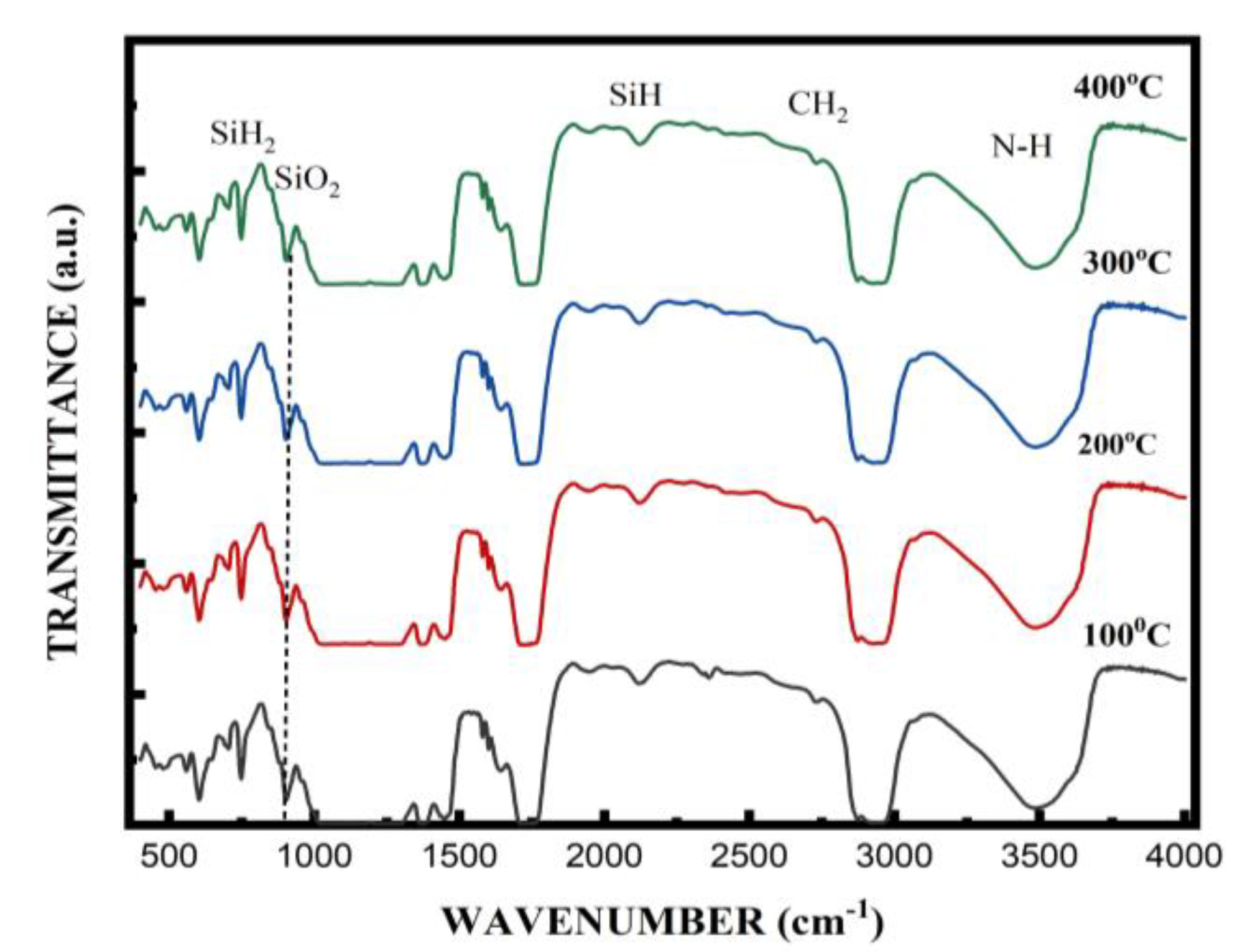
Figure 7.
SEM of ML nc-Si/Si thin films (a) cross-sectional view of top-layer and (b) Topographic view as a function of annealing temperature.
Figure 7.
SEM of ML nc-Si/Si thin films (a) cross-sectional view of top-layer and (b) Topographic view as a function of annealing temperature.
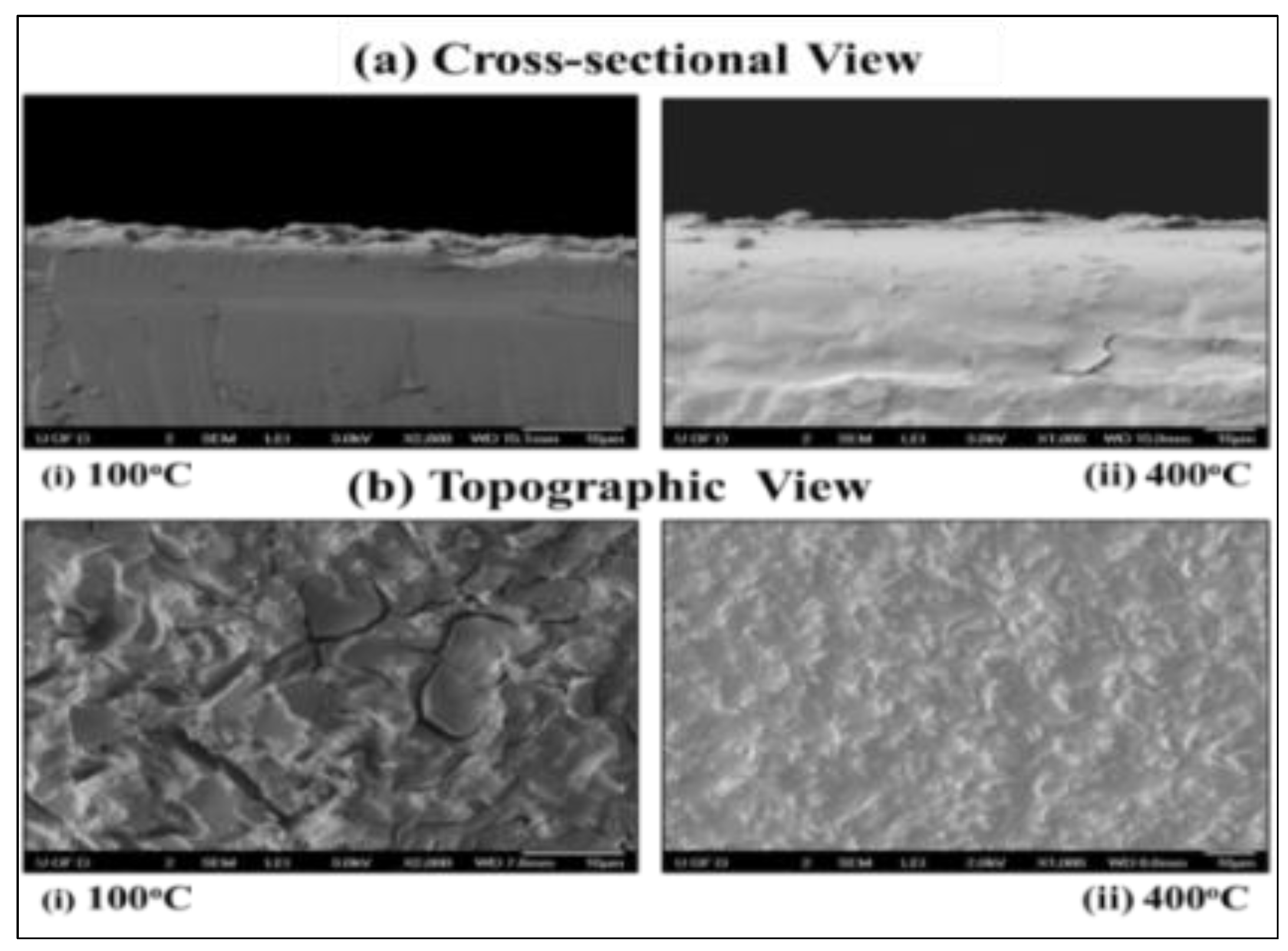
Figure 8.
Optical transmission spectra of the ML nc-Si/Si thin films after 240 min UV illumination as a function of annealing temperature.
Figure 8.
Optical transmission spectra of the ML nc-Si/Si thin films after 240 min UV illumination as a function of annealing temperature.
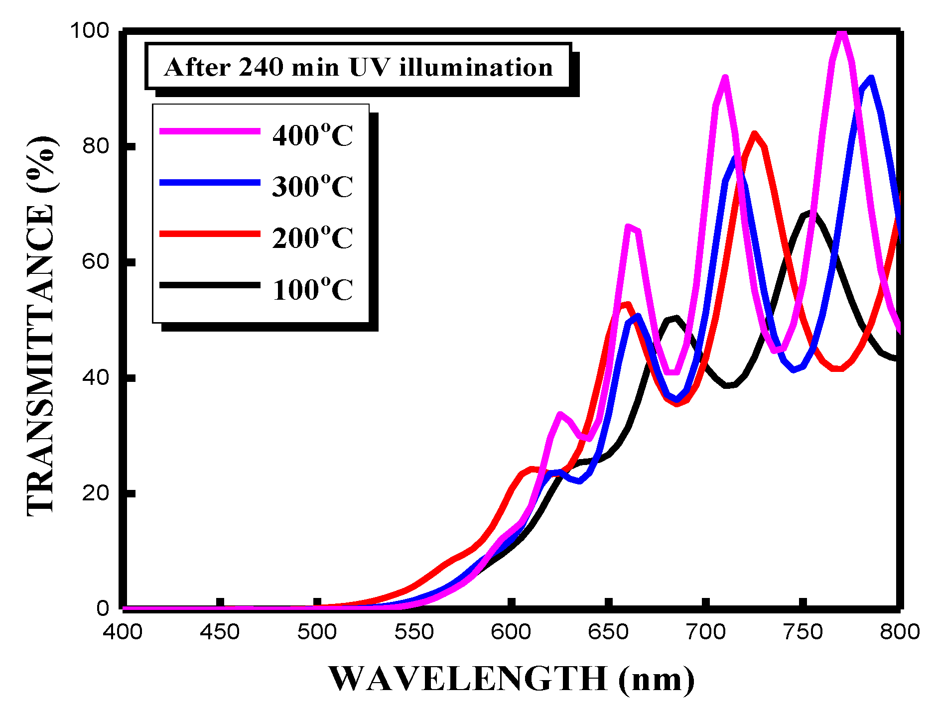
Figure 9.
Optical band gap energy of ML nc-Si/Si as a function of annealing temperature.
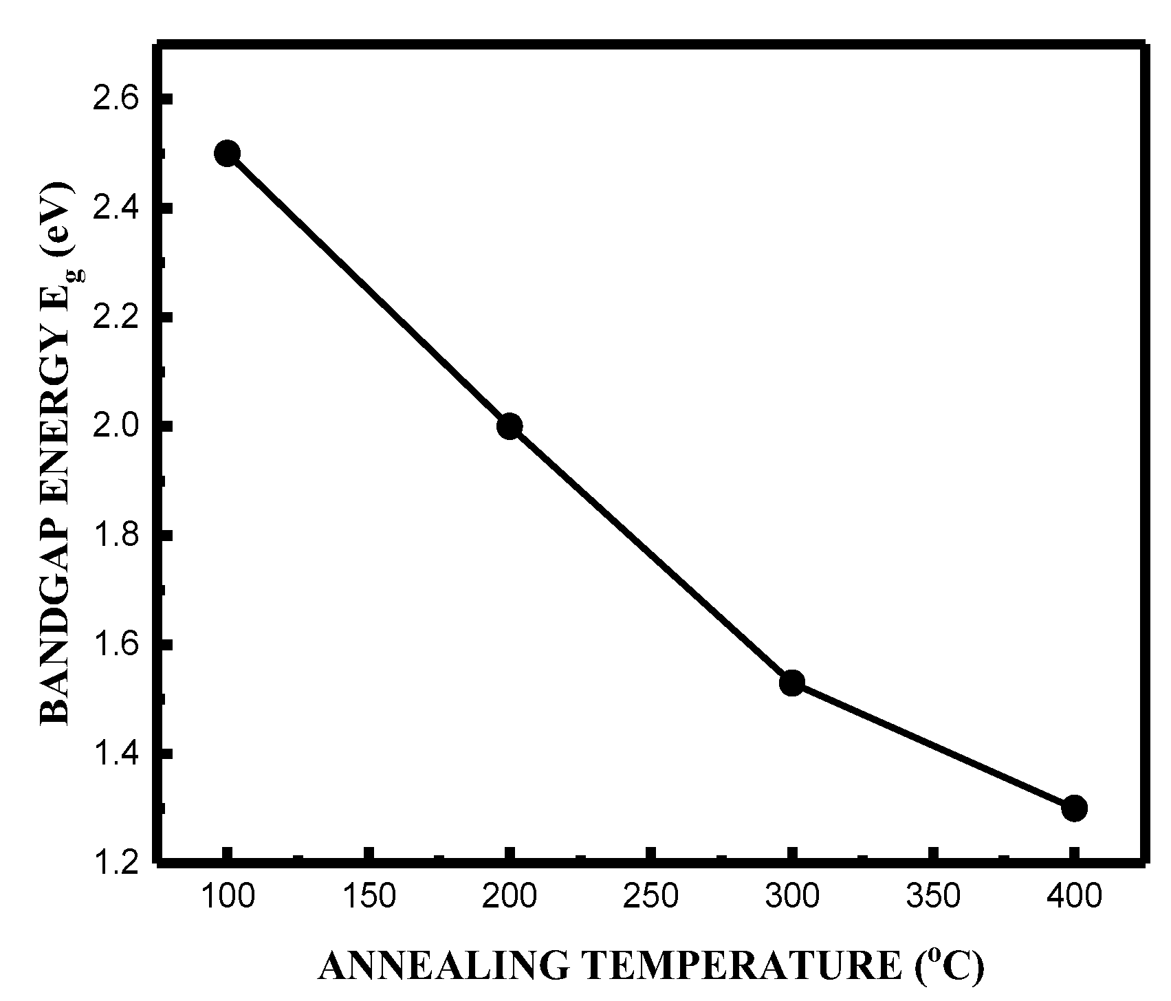
Figure 10.
shows the change of ML nc-Si/Si thin film thickness and refractive index as a function of annealing temperature.
Figure 10.
shows the change of ML nc-Si/Si thin film thickness and refractive index as a function of annealing temperature.
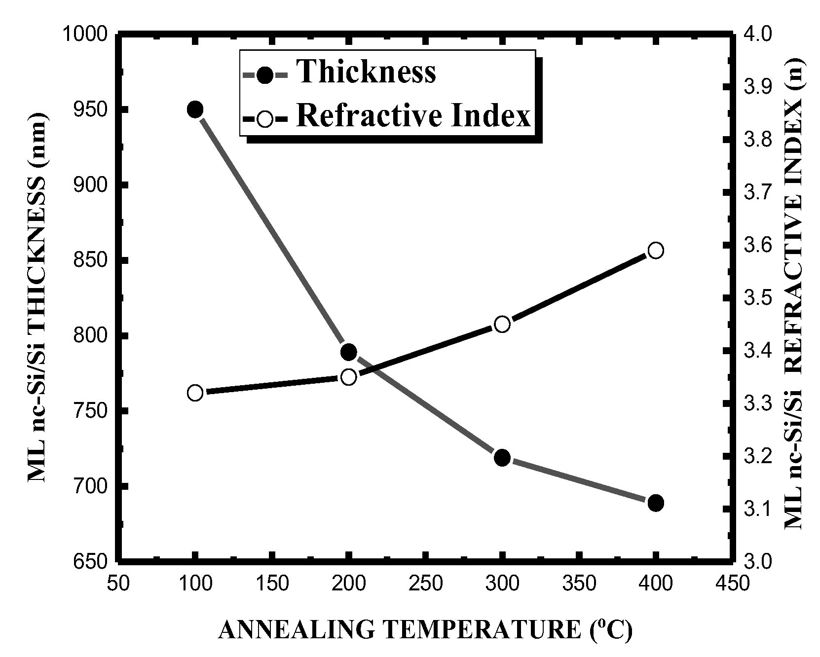
Figure 11.
Mobility and Resistivity measurements of ML nc-Si/Si thin films deposited on Si substrate.
Figure 11.
Mobility and Resistivity measurements of ML nc-Si/Si thin films deposited on Si substrate.
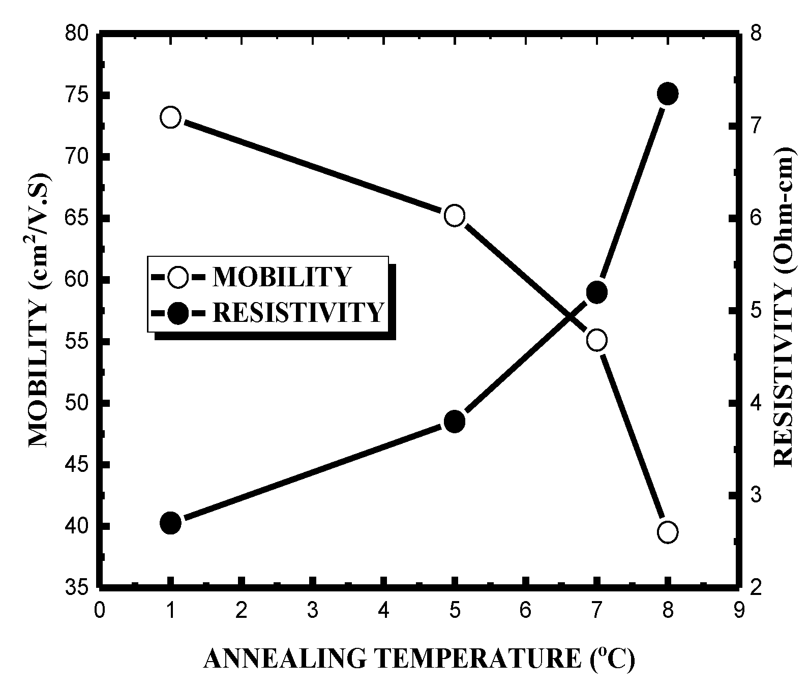

Table 1.
Wet cleaning Conditions used to disinfect substrates and remove any fragments of material of oil.
Table 1.
Wet cleaning Conditions used to disinfect substrates and remove any fragments of material of oil.
| Substrate | Acetone | Ethanol &DI-Water |
| P-type (100) | 15 min | 15 min each |
| Silicon (Si) |
Table 2.
ition parameters for ML nc-Si/Si Thin-Film growth.
| Substances | Quantity |
| TEOS (1 mole) EtOH (2 mole) 0.0013 M CTAB Di-Water CTAB +TEOS Sol. 0.1M HCl + TEOS Sol. nc-Si powder Add SiOx Sol-Gel Spin-Coater rpm Deposition Time (SiOx & Thin Film) SiOx Annealing Temperature (oC) and Time (hrs) Aging Time of SiOx Sol-Gel ML nc-Si/Si Annealing Temperature (oC) |
8.33 mL 3.69 mL 0.2 gm 200 mL 6.01 mL 6.01 mL 0.10 gm 5.0 mL 11,800 10 sec 50 2 8 days 100-400 oC |
Disclaimer/Publisher’s Note: The statements, opinions and data contained in all publications are solely those of the individual author(s) and contributor(s) and not of MDPI and/or the editor(s). MDPI and/or the editor(s) disclaim responsibility for any injury to people or property resulting from any ideas, methods, instructions or products referred to in the content. |
© 2025 by the authors. Licensee MDPI, Basel, Switzerland. This article is an open access article distributed under the terms and conditions of the Creative Commons Attribution (CC BY) license (http://creativecommons.org/licenses/by/4.0/).
Copyright: This open access article is published under a Creative Commons CC BY 4.0 license, which permit the free download, distribution, and reuse, provided that the author and preprint are cited in any reuse.


