
Submitted:
25 November 2025
Posted:
26 November 2025
You are already at the latest version
Abstract
This paper presents a self-contained startup charging circuit designed for energy harvesting batteryless IoT devices. The proposed circuit consists of a current biasing block, a current mirror, a reference voltage generator, and a comparator circuit. The current biasing circuit drives the current mirror, which supplies the charging current to the energy storage element. Simultaneously, the reference voltage generator—also biased by the current source produces a stable DC reference voltage. When the energy storage device (e.g., a supercapacitor) lacks sufficient charge, the comparator enables the charging path by activating the current biasing and mirror circuits. Once adequate energy is stored, the comparator disables these circuits to prevent overcharging. This self-contained solution is intended to autonomously initialize and manage the cold-start charging process in energy harvesting systems without relying on external controllers.
Keywords:
startup charging circuit
; self-contained charger
; energy harvesting
; batteryless IoT devices
Introduction
In batteryless Internet of Things (IoT) devices, energy harvesting systems rely heavily on supercapacitors as energy storage elements due to their high power density, rapid charging capability, and long cycle life [1,2,3,4]. However, efficiently charging supercapacitors, especially during cold- start conditions when the device has no pre-existing energy, remains a significant design challenge.
The charging circuit must operate reliably with low input power, avoid the need for external controllers, and ensure seamless startup across varying environmental conditions.
Moreover, the charging circuit plays a critical role in the entire system’s operation it determines how quickly and efficiently the IoT node can become active, respond to sensed data, and maintain energy autonomy [5,6,7,8]. Any inefficiency or dependence on external control can compromise system performance, especially in intermittent or unpredictable energy environments. Therefore, developing a robust and efficient charging circuit that is self-starting and self-contained is essential to enabling practical and scalable deployment of batteryless IoT solutions.
In most existing designs, the charging circuit requires an external current source and reference voltage to operate effectively [9]. This paper presents a self-contained charging circuit with internal means for generating both the bias current and reference voltage. This design eliminates the need for external control elements, enabling autonomous startup and improving energy efficiency for batteryless IoT applications.
The paper [10,11,12,13,14] discloses a device with an external nano-watt bandgap voltage reference circuit with six-stage PTAT voltage generator where the stages, each equipped with a differential pair and current mirror, are cascaded in such a way that produces sufficient positive temperature coefficients. The disclosure also provides a separate nano- ampere current reference circuit that serves as the current source for the charging circuit. Crucially, such use of external current source and voltage reference circuit results in a complex circuit design that requires a substantial physical area when manufactured.
The works presented in [15,16] describe a startup circuit that (i) forces an arbitrary bias-generating circuit into a steady-current state during startup by conducting charging current from an external current source, and (ii) disconnects the external source afterward using switching means. When such an approach is adapted to charging circuits for energy storage devices, it inherits key design limitations—most notably, the dependence on an external current source.
In contrast, the circuit proposed in this work is self- contained, integrating all essential functions—biasing, voltage reference generation, and switching control into a single autonomous block. This design simplifies system integration and enables reliable cold-start operation in batteryless IoT systems. The objective of this paper is to address and overcome the limitations of previous approaches by eliminating the need for external control elements.
The rest of this paper is organized as follows. Section 2 presents the design and architecture of the proposed self-contained charging circuit. Section 3 discusses the simulation results, including corner and Monte Carlo analyses, validating the circuit’s performance under various operating conditions. Section 4 details the post-simulation evaluation and actual chip measurement results. Finally, Section 5 concludes the paper by summarizing the key contributions and highlighting the advantages of the proposed design for energy harvesting applications.
Proposed Charging Circuit
Figure 1 illustrates the role and architecture of the proposed self-contained charging circuit within an energy harvesting system. Figure 1a shows a system-level diagram where multiple energy sources (thermal, solar, RF) are funneled through an energy converter to power a load. The proposed startup charging circuit is used to charge a supercapacitor, providing a reliable energy buffer for cold-start conditions [17].
Figure 1b presents the internal block diagram of the proposed charging circuit. Unlike conventional designs, this implementation integrates all critical functions—startup circuit, current biasing, reference voltage generation, current mirror, comparator, and output buffer into a single autonomous module. This self-contained architecture enables reliable cold- start operation without the need for external biasing or reference inputs, thereby enhancing integration and suitability for batteryless IoT applications.
Previous startup charging circuits, such as those presented in [10], typically rely on external components such as a high-voltage pump (Vpump), a fixed reference voltage (Vref), and external bias sources to enable operation. These dependencies pose critical limitations in energy harvesting applications particularly during cold-start conditions where no external energy sources are guaranteed at startup.
In contrast, the circuit proposed in this work is fully self-contained, integrating internal current biasing, voltage reference generation, and comparator control into a single autonomous block. This architecture eliminates the need for any external startup assistance, thereby enabling reliable cold-start operation and simplifying system integration in batteryless IoT devices. The self-contained design directly addresses the key challenges of energy-autonomous systems by ensuring that all essential charging functions are internally generated and managed.
Figure 2b shows the simplified schematic of the proposed charging circuit. The start-up circuit transistors are labelled by SU1, SU2 and SU3 which provides initial bias to the current biasing circuit through the gate of SU2 and the drain of SU3. The current biasing circuit generates the current reference for the entire block. The fixed DC reference voltage generated at the reference voltage is fed to the comparator circuit.
Resistor Rv and transistor RV2 are configured to serve as PTAT and CTAT generators, respectively, such that the voltage Vref is temperature-insensitive. Rv and RV2 are scaled in size and parameters so that their linear temperature coefficients are equal in magnitude and opposite in sign. Such configuration of the reference voltage generator enables the charging circuit of this paper to forego other components (such as six-stage PTAT voltage generator, as in the prior art) and consequently minimize the layout area.
The current mirror circuit receives current from the current biasing circuit through CM1, mirroring to CM3 and generates charging current at the VSC terminal.
Under normal operation, the current biasing circuit generates a constant current which translates to a bias voltage at Vbias. Transistor CM1 then mirrors the drain current at CB3 through Vbias Similarly, the drain current at CM1 is mirrored to CM2 and CM3.
When charging the energy storage device, the drain voltage at CM3 or the voltage VSC of the energy storage device ramps up from zero (i.e, at zero charge) to the reference voltage Vref (i.e., at sufficiently high or full charge). When the energy storage is fully charged that its voltage VSC surpasses the reference voltage Vref, the comparator circuit outputs a signal that activates the shutdown transistors (SD1 and SD2) and pulls the gates of CM3 and CM2, this disabling the entire charging circuit into a standby state. The charging circuit is now uncoupled from the energy storage device and will stop the charging current. The charging circuit remains disabled until the voltage VSC of the energy storage device is less than the reference voltage Vref.
In this paper, the reference voltage achieves a value of 700mV with minimal swing under varying process parameters, supply voltage, and operating temperature. It is designed to operate at a supply voltage ranging from 900mV to 1.9V and an operating temperature ranging from −40◦C to 85◦C. The charging current reaches 31.21mA considering the worst case slow-slow corner simulation. The proposed charging circuit is implemented using the 22nm fully depleted silicon-on-insulator (FDSOI) technology and is integrated into a working energy storage harvesting system.
Simulation Results and Discussion
Circuit simulation was performed to verify the performance of the design while considering the target specification shown in Table 1. As part of the requirements, the design should operate in AVDD minimum voltage of 0.9V and up to the maximum supply voltage of 1.8V. The charging current across Supercapacitor (SC) is expected to be from 1mA to 50mA including worst case conditions. Supercapacitor voltage (VSC) full charge should be from 700mV to 900mV.
Corner Simulation Results
Using block simulation setup, behavior of charging circuit is tested. At typical simulation, transient analysis ran from 0s to 5000s, 25◦C and nominal model. Figure 3 shows the typical simulation waveform plot of VSC, Vcomp, and the charging current showing meeting the target specifications.
As shown in Figure 3, the full battery voltage is measured at the stable state of VSC pin, which is also connected to the supercapacitor, after the ramp up or the charging time. The Vcomp signal is “high” at the beginning of the ramp and toggles to “low” after it detects the battery full in the VSC pin, where the VSC voltage surpasses the Vref voltage at the comparator.
The block is also tested for maximum VDD of 1.8V and typical conditions for temperature and process parameters. Figure 4 shows the resulting graph for these conditions.
Further verification through corner simulation was performed to confirm the functionality of the proposed charger block. Table 2 presents the tabular data summarizing the 136 results of corner simulation.
Corner simulations were tested using three temperature variations (−40◦C, 25◦C and 85◦C), different model variations (slow, typical, fast) and two levels of VDD (1.0V and 1.8V). All results are passed and within the target specifications, no abnormal response was observed.
Monte Carlo Simulation Results
To validate the robustness of the proposed charging circuit design, Monte Carlo simulation was executed. The simulation was done under minimum and maximum condition of temperature (−40◦C and 85◦C), two VDD values (1.0V and 1.8V), sampling of 200 runs, and using mismatch variation option. Table 3 summarizes the Monte Carlo simulation results separated by the VDD value. All results are within the target specifications.
Evaluation Results and Post Simulation
Performance Comparison
Table 4 presents a comparative analysis of the proposed self-contained charging circuit against the state-of-the-art energy harvesting solutions. Unlike traditional designs that rely heavily on charge pumps or complex multi-stage rectification, this work demonstrates a self-contained charging topology capable of delivering a significantly higher output current of 25mA, with a modest output voltage of 0.7V–0.8V, making it well-suited for low-voltage supercapacitor charging in batteryless IoT systems. Prior works, such as those in [6,10], and [11], exhibit lower current outputs ranging from 10µA to 395µA, primarily due to limitations imposed by their charge pump-based or rectifier-based architectures. Moreover, while earlier studies used older CMOS technologies (down to 0.18µm), this work achieves its performance on a 22nm FDSOI process, emphasizing its scalability and integration potential. The results validate the effectiveness of a fully self-contained circuit in delivering 160 high current without relying on auxiliary power stages or external control logic.
Post Simulation Results
The functionality of the charging circuit was evaluated under different temperature variations, VDD, and using 5 samples. Since the proposed design is a stand-alone block, the setup is simplified and tested activating the charging circuit only by supplying VDD. Figure 5 shows the evaluation results or actual chip testing of chips 6 to 10, labelled C6 to C10 in the graph, and post simulation at 25◦C. As shown in the figure, there is no significant difference observed comparing post simulation and the measurement of the 5 samples tested.
Figure 6 shows the comparison between actual chip testing and post simulation results across −35◦C, 25◦C, and 100◦C. As observed, the simulated output slightly overestimates the measured VSC, but the temperature trend is consistent, confirming reliable behavior under varying thermal conditions.
Chip Layout and Implementation
Figure 7a shows the layout of the charging core, designed and implemented in 22nm FDSOI technology. It highlights the transistor-level design of key components such as power switches, capacitors, and control circuitry, all optimized for efficient energy transfer. Figure 7b presents the full-chip layout, with the entire energy harvesting system—including the charging circuit occupying a total area of 1000um x 400um. The design is intended for packaging in a QFN40 (5mm x 5mm) package. This layout illustrates the system-level integration of the proposed charging circuit, including its connections to power management, energy storage, and control blocks, with routing carefully optimized to minimize parasitic losses. Figure 7c shows the chip die micrograph, illustrating the fabricated silicon layout of the charging circuit with visible pad placements and key functional blocks. Finally, Figure 7d Testing set-up with DC Power Analyzer and Thermal Chamber for performance validation and measurement.
Conclusions
This paper presented a self-contained charging circuit designed for energy harvesting systems. The proposed design eliminates the need for external current and voltage references by integrating a current biasing circuit and a temperature-insensitive reference voltage generator. A simplified yet effective control mechanism using a comparator circuit enables autonomous switching between active charging and standby states, optimizing energy usage.
Simulation results, including typical, corner, and Monte Carlo analyses, confirm the circuit’s robustness across a wide range of process, voltage, and temperature variations. The charging current meets the target specifications, and the reference voltage remains stable across operating conditions. Furthermore, post-layout and actual chip testing show strong agreement with simulation results, validating the design’s functionality and reliability in a fabricated silicon implementation.
Overall, the proposed charging circuit demonstrates high efficiency, compactness, and suitability for integration into low-power energy harvesting applications, such as systems utilizing supercapacitors for energy storage.
Author Contributions
Conceptualization, M.L., K.K.A., J.A.H., and C.G.A.; methodology, M.L., K.K.A., and R.M.C.; validation, M.L., K.K.A., J.A.H., and C.G.A.; formal analysis, M.L. and R.M.C.; investigation, M.L. and R.M.C.; resources, C.G.A.; data curation, M.L. and R.M.C.; writing—original draft preparation, M.L. and R.M.C.; writing—review and editing, C.G.A., M.L., and R.M.C.; supervision, C.G.A., X.Z., and Y.S.; project administration, C.G.A.; funding acquisition, C.G.A. and Y.S. All authors have read and agreed to the published version of the manuscript.
Funding
This work was supported by the Department of Science and Technology – Science Education Institute (DOST-SEI) through the Center for Integrated Circuits Design (CICD-Microlab) at Mindanao State University – Iligan Institute of Technology (MSU-IIT), under the DOST-PCIEERD-funded Center for Integrated Circuits and Devices Research (CIDR) program, titled “Energy Harvesting for Battery-less IoT Device Operation.” Additional support was provided by XINYX DESIGN.
Data Availability Statement
The data presented in this study are available in article.
Acknowledgments
The authors gratefully acknowledge the support of the Department of Science and Technology – Science Education Institute (DOST-SEI) through the Center for Integrated Circuits Design (CICD-Microlab) at Mindanao State University – Iligan Institute of Technology (MSU-IIT). This research is part of the preliminary circuit design activities under a project funded by the Department of Science and Technology (DOST), Philippines, and managed by DOST-PCIEERD through the Center for Integrated Circuits and Devices Research (CIDR) program, titled “Energy Harvesting for Battery-less IoT Device Operation.”. The authors also thank XINYX DESIGN for their partnership and co-design contributions in developing the circuit presented in this work.
Conflicts of Interest
The authors declare no conflict of interest.
References
- Manabat, F.R., Dayondon, J.H.P., Fernandez, J.C.R., Adrivan, K.K., & Hora, J.A. (2023). A design of high efficiency non-time division multiplexing battery-less and self-powered multi-input single-inductor single-output using 22nm FDSOI technology. Proceedings of the 2023 22nd International Symposium on Communications and Information Technologies (ISCIT), 1–6. IEEE.
- Ju, Q., & Zhang, Y. (2017). Predictive power management for internet of battery-less things. IEEE Transactions on Power Electronics, 33(1), 299–312.
- Yahya, F., Lukas, C.J., Breiholz, J., Roy, A., Patel, H.N., Liu, N., Chen, X., Kosari, A., Li, S., Akella, D., et al. (2017). A battery-less 507nW SoC with integrated platform power manager and SiP interfaces. Proceedings of the 2017 Symposium on VLSI Circuits, C338–C339. IEEE.
- Lukas, C.J., Yahya, F.B., Breiholz, J., Roy, A., Chen, X., Patel, H.N., Liu, N., Kosari, A., Li, S., Kamakshi, D.A., et al. (2019). A 1.02 W battery-less, continuous sensing and post-processing SiP for wearable applications. IEEE Transactions on Biomedical Circuits and Systems, 13(2), 271–281.
- Du, S., Amaratunga, G.A., & Seshia, A.A. (2018). A cold-startup SSHI rectifier for piezoelectric energy harvesters with increased open-circuit voltage. IEEE Transactions on Power Electronics, 34(1), 263–274.
- Chen, P.-H., Ishida, K., Zhang, X., Okuma, Y., Ryu, Y., Takamiya, M., & Sakurai, T. (2010). 0.18-V input charge pump with forward body biasing in startup circuit using 65nm CMOS. Proceedings of the IEEE Custom Integrated Circuits Conference, 1–4. IEEE.
- Ballo, A., Grasso, A.D., & Palumbo, G. (2019). A review of charge pump topologies for the power management of IoT nodes. Electronics, 8(5), 480. Available online: https://www.mdpi.com/2079-9292/8/5/480.
- Jung, J., & Kwon, I. (2023). A capacitive DC-DC boost converter with gate bias boosting and dynamic body biasing for an RF energy harvesting system. Sensors, 23(1), 395. Available online: https://www.mdpi.com/1424-8220/23/1/395.
- Comaling, R.M., Zhu, X., & Hora, J.A. (2024). A 95.71% power efficiency DC-DC PFM boost converter with recursive voltage supply technique for low-power energy harvesting application. Proceedings of the 2024 IEEE 10th International Symposium on Microwave, Antenna, Propagation and EMC Technologies for Wireless Communications (MAPE), 1–4. IEEE.
- Huang, H.-Y., Yen, S.-Z., Chen, J.-H., Hong, H.-C., & Cheng, K.-H. (2016). Low-voltage indoor energy harvesting using photovoltaic cell. Proceedings of the 2016 IEEE 19th International Symposium on Design and Diagnostics of Electronic Circuits & Systems (DDECS), 1–4. IEEE.
- H. -Y. Huang, C. O. Mocorro, J. Pinaso and K. -H. Cheng, “Indoor energy harvesting using photovoltaic cell for battery recharging,” 2013 IEEE 16th International Symposium on Design and Diagnostics of Electronic Circuits Systems (DDECS), Karlovy Vary, Czech Republic, 2013, pp. 224-227.
- Osaki, Y., Hirose, T., Kuroki, N., & Numa, M. (2013). 1.2-V supply, 100-nW, 1.09-V bandgap and 0.7-V supply, 52.5-nW, 0.55-V subbandgap reference circuits for nanowatt CMOS LSIs. IEEE Journal of Solid-State Circuits, 48(6), 1530–1538.
- Adrivan, K.K.C., & Hora, J.A. (2022). A nano-watt, subthreshold self-biased CMOS voltage reference without resistors and BJT. Proceedings of the TENCON 2022 IEEE Region 10 Conference, 1–5. IEEE.
- Comaling, R.M., Diangco, M.M.C., & Hora, J.A. (2023). 22nm FDSOI forward body biasing in designing ultra-low power, high PSRR voltage reference for IoT power management applications. Proceedings of the TENCON 2023 IEEE Region 10 Conference, 1–5. IEEE.
- Ruetz, E.J. (1992). Bias start-up circuit. European Patent EP0515065A1, Filed: May 8, 1992; Published: Nov 25, 1992.
- Hwang, Y.-S., Wang, S.-C., Yang, F.-C., & Chen, J.-J. (2007). New compact CMOS Li-ion battery charger using charge-pump technique for portable applications. IEEE Transactions on Circuits and Systems I: Regular Papers, 54(4), 705–712.
- Shi, X., Cai, M., & Jiang, Y. (2024). Key role of cold-start circuits in low-power energy harvesting systems: A research review. Journal of Low Power Electronics and Applications, 14(4). Available online: https://www.mdpi.com/2079-9268/14/4/55.
- Bose, S.; Anand, T.; Johnston, M.L. Integrated cold-start of a boost converter at 57mV using cross-coupled complementary charge pumps and ultra-low-voltage ring oscillator. IEEE J. Solid-State Circuits 2019, 54, 2867–2878. [Google Scholar] [CrossRef] [PubMed]
- Goeppert, J.; Manoli, Y. Fully integrated startup at 70mV of boost converters for thermoelectric energy harvesting. IEEE J. Solid-State Circuits 2016, 51, 1716–1726. [Google Scholar] [CrossRef]
- Yu, H.; Wang, G.; Lian, Y. A batteryless single-inductor boost converter with 190mV self-startup voltage for thermal energy harvesting. IEEE Trans. Circuits Syst. II 2019, 66, 889–893. [Google Scholar] [CrossRef]
- Ramadass, Y.K.; Chandrakasan, A.P. A battery-less thermoelectric energy harvesting interface circuit with 35mV startup voltage. IEEE J. Solid-State Circuits 2011, 46, 333–341.
- Kouhalvandi, L.; Dragomirescu, D.; Vasic, M. A review on self-startup circuits for ultra-low-power energy harvesting interfaces. J. Low Power Electron. Appl. 2018, 8, 40.
- Zhang, Y.; Wu, C.; Zeng, Y. A 7.5 mV input and 88.
- Li, J.; Shao, Y.; Li, Y.; Xu, D.; Guo, J. A fully integrated energy harvester with efficient cold-start and three-domain MPPT. IEEE Trans. Power Electron. 2018, 33, 10445–10458.
- Sudevalayam, S.; Kulkarni, P. Energy harvesting sensor nodes: Survey and implications. IEEE Commun. Surv. Tutor. 2011, 13, 443–461.
- Pinuela, M.; Mitcheson, P.D.; Lucyszyn, S. Ambient RF energy harvesting in urban and semi-urban environments. IEEE Trans. Microw. Theory Techn. 2013, 61, 2715–2726.
- Lian, Q.; Han, P.; Mei, N. A review of converter circuits for ambient micro energy harvesting. Micromachines 2022, 13, 2222.
- S¸ahin, M.E.; Blaabjerg, F.; Sangwongwanich, A. A comprehensive review on supercapacitor applications and developments. Energies 2022, 15, 674. https://www.mdpi.com/1996-1073/15/3/674 285.
- Vullers, R.J.M.; van Schaijk, R.; Doms, I.; Van Hoof, C.; Mertens, R. Micropower energy harvesting. Solid-State Electron. 2009, 53, 684–693. 287.
- Ottman, G.K.; Hofmann, H.F.; Bhatt, A.C.; Lesieutre, G.A. Adaptive piezoelectric energy harvesting circuit for wireless remote power supply. IEEE Trans. Power Electron. 2002, 17, 669–676.
- Dini, M.; Romani, A.; Filippi, M.; Fiegna, C.; Masotti, D.; Tartagni, M. A nano-current power management IC for multiple heterogeneous energy harvesting sources. IEEE Trans. Power Electron. 2015, 30, 5665–5680.
- Beeby, S.; White, N. Energy Harvesting for Autonomous Systems; Artech House: Boston, MA, USA, 2010.
Figure 1.
(a) System-level diagram of an energy harvesting application incorporating the proposed startup charging circuit to charge a supercapacitor [17]. (b) Block diagram of the proposed self- contained charging circuit, showing its main functional components including the startup circuit, internal biasing, reference generation, current mirror, comparator, and output buffer.
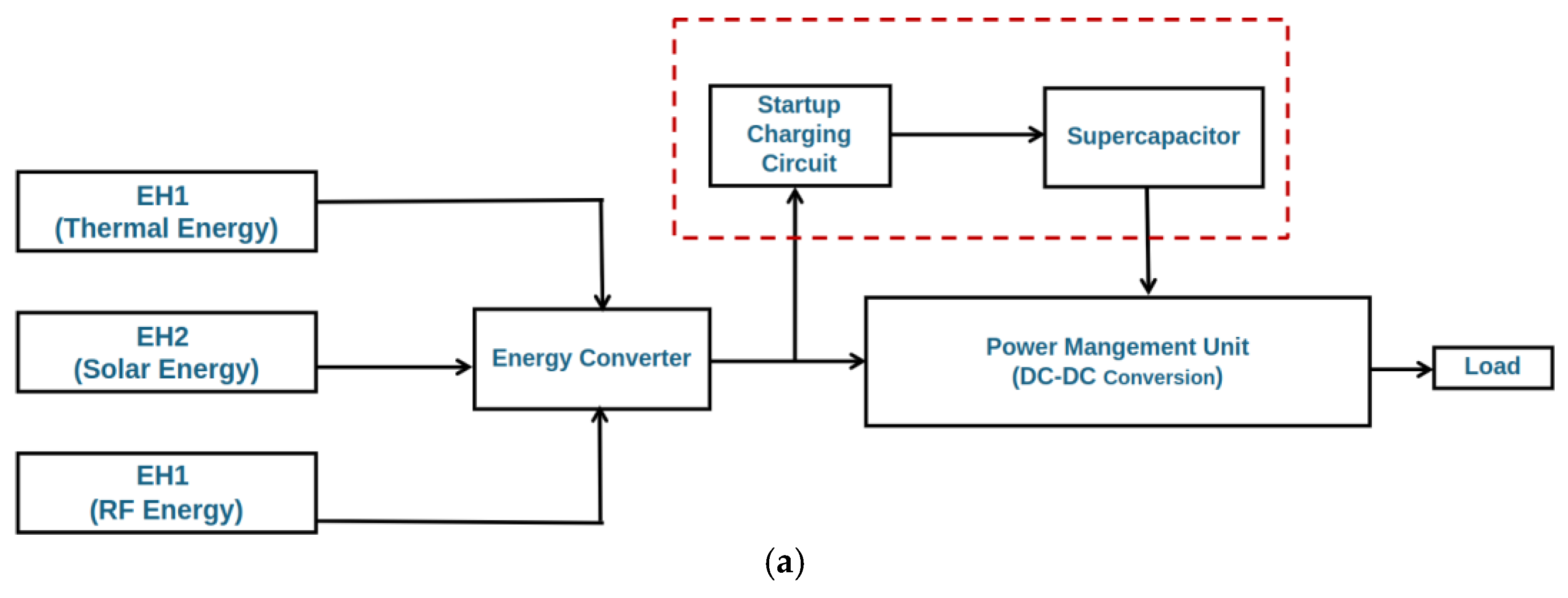
Figure 2.
The proposed self-contained charging circuit for energy-harvesting batteryless IoT devices.
Figure 2.
The proposed self-contained charging circuit for energy-harvesting batteryless IoT devices.
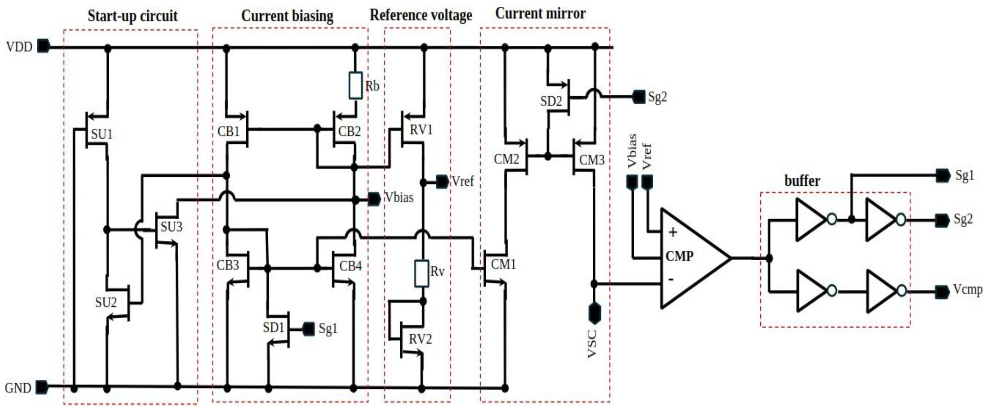
Figure 3.
Typical simulation results for VDD=1.0V.
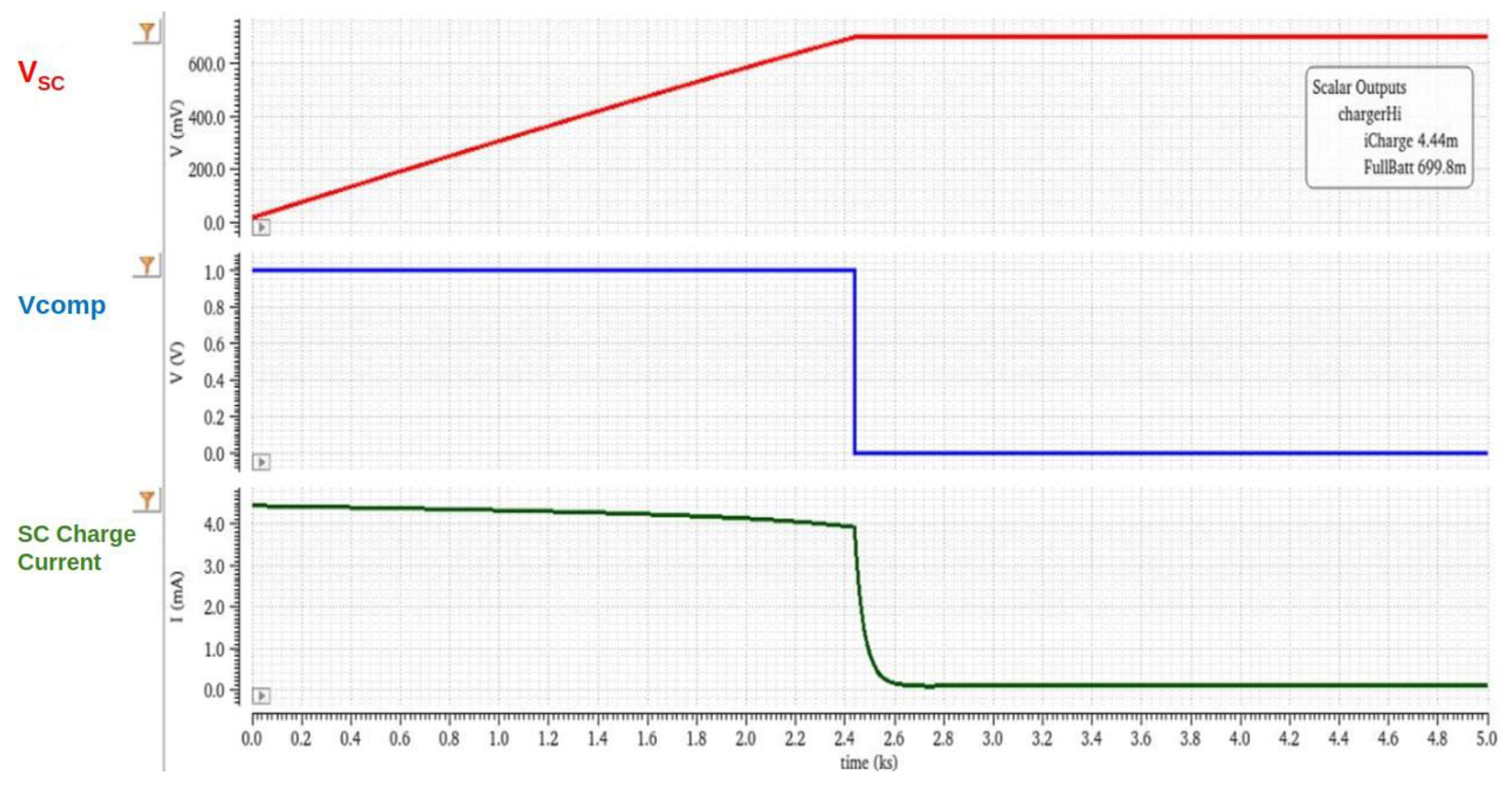
Figure 4.
Typical simulation results for VDD=1.8V.
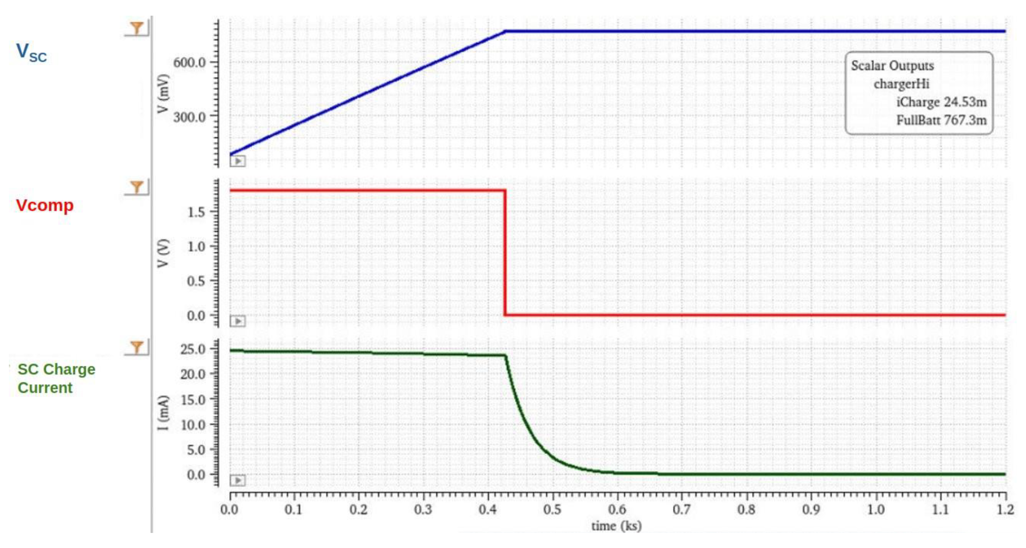
Figure 5.
Supercapacitor voltage (VSC) measurement. Actual chip testing of 5 samples comparing with post simulation at 25◦C.
Figure 5.
Supercapacitor voltage (VSC) measurement. Actual chip testing of 5 samples comparing with post simulation at 25◦C.
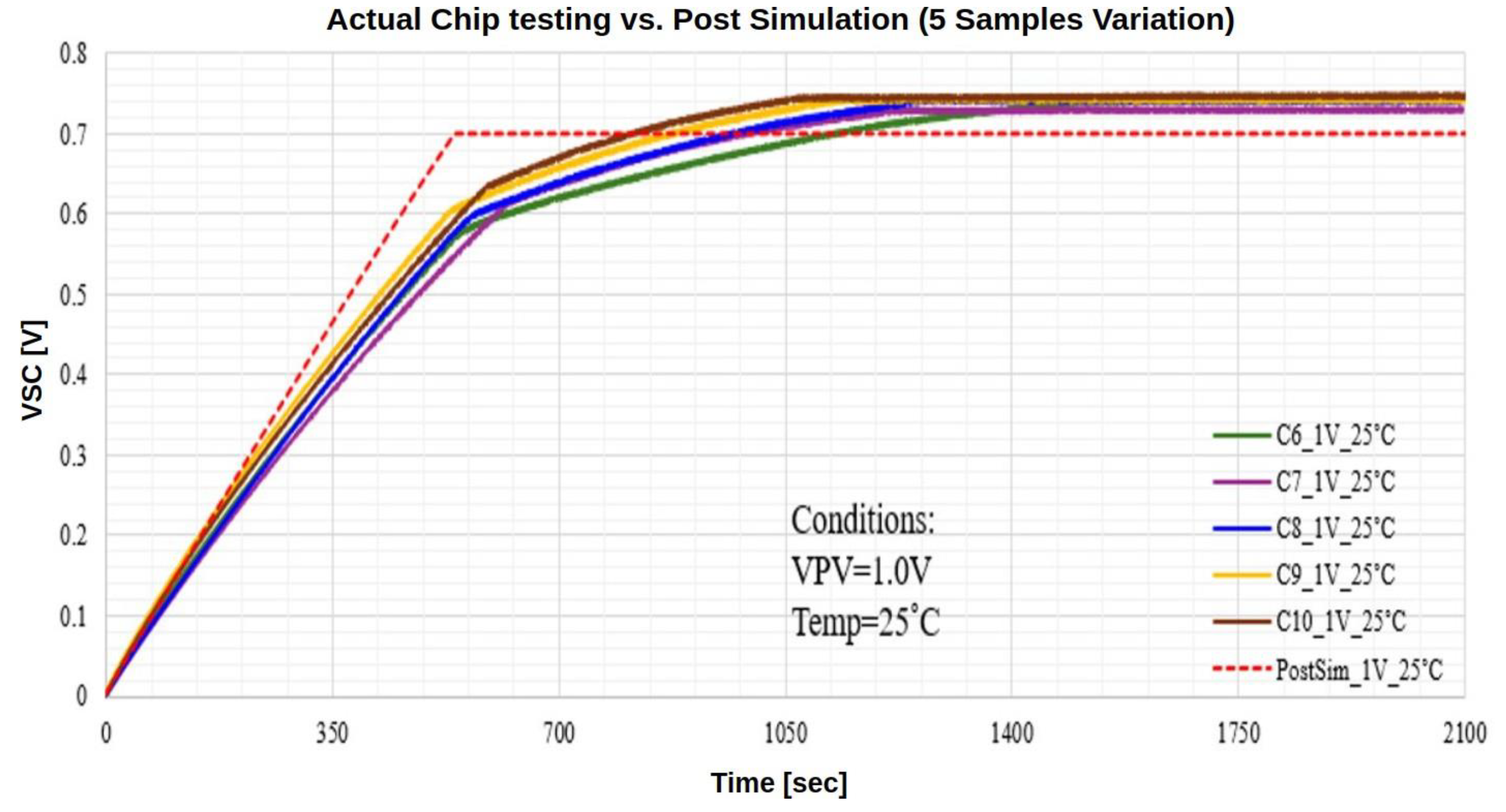
Figure 6.
Supercapacitor voltage (VSC) measurement. Actual chip testing of Chip8 compared with post simulation in three temperatures.
Figure 6.
Supercapacitor voltage (VSC) measurement. Actual chip testing of Chip8 compared with post simulation in three temperatures.
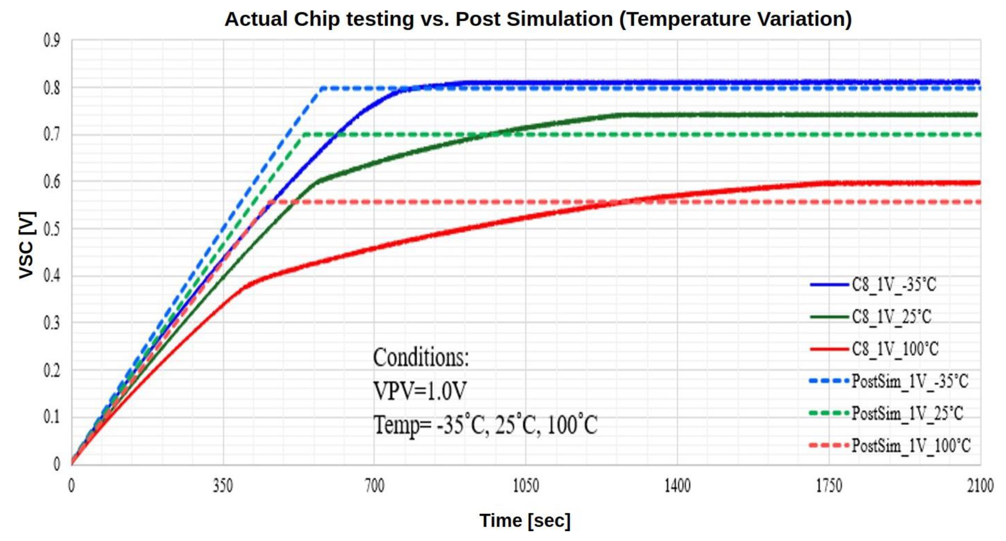
Figure 7.
Chip layout and implementation: (a) Charging core layout (b) Full-chip layout of the energy harvesting system with integrated charging circuit (c) Chip Die Micrograph (d) Testing set-up with DC Power Analyzer and Thermal Chamber.
Figure 7.
Chip layout and implementation: (a) Charging core layout (b) Full-chip layout of the energy harvesting system with integrated charging circuit (c) Chip Die Micrograph (d) Testing set-up with DC Power Analyzer and Thermal Chamber.
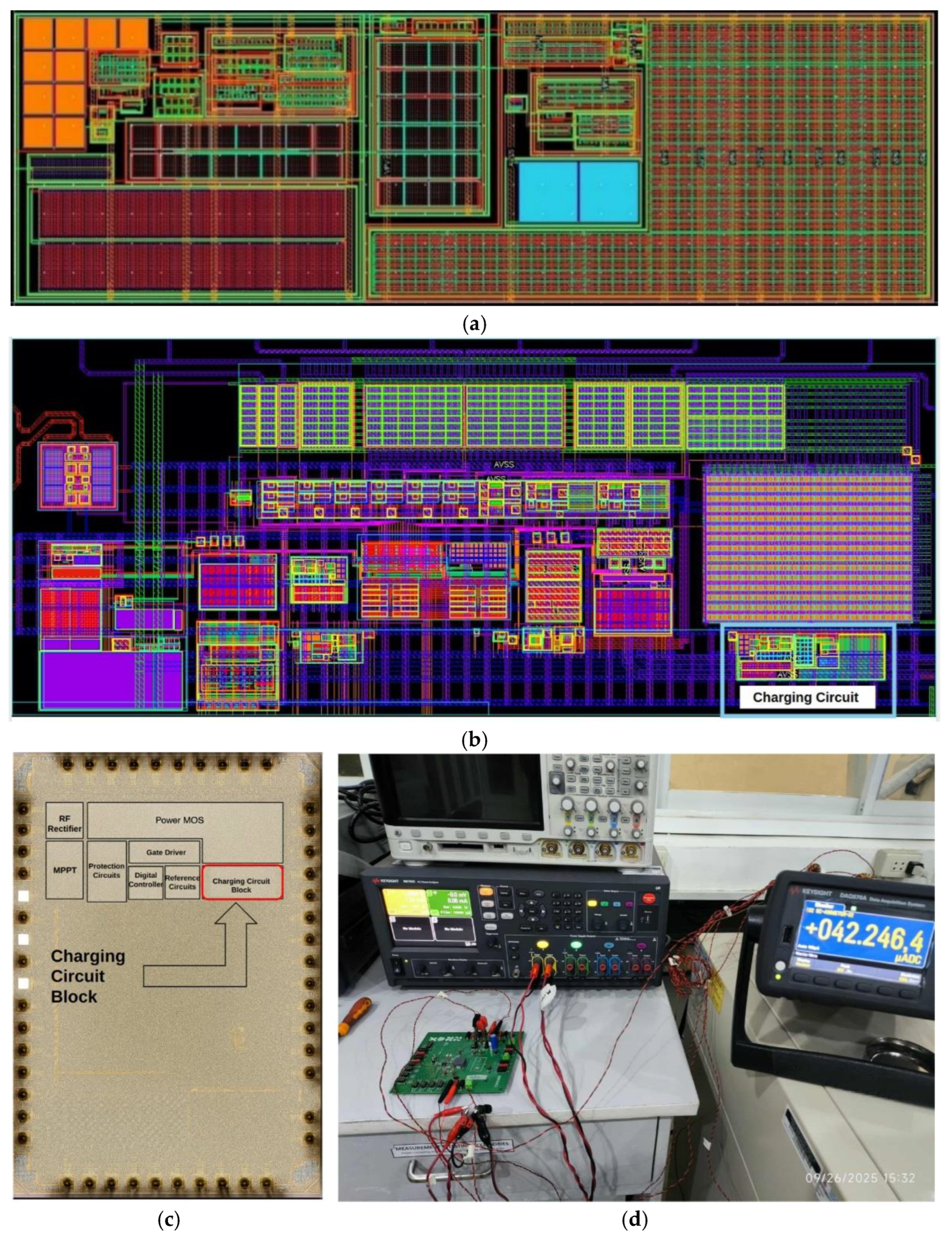

Table 1.
Target specification of proposed charging circuit.
| Parameters | Symbol | Minimum | Typical | Maximum | Unit |
|---|---|---|---|---|---|
| Supply Voltage | AVDD | 0.9 | – | 1.8 | V |
| SC Charge Current | iCharge | 1 | 20 | 50 | mA |
| Reference Voltage | Vref | 0.7 | 0.75 | 0.8 | V |
| Supercapacitor Voltage | VSC | 0.6 | 0.7 | 0.8 | V |
Table 2.
Corner Simulation Results.
| Parameters | ForVDD = 1.0 V | ForVDD = 1.8 V | Unit | ||||
| Min | Typ | Max | Min | Typ | Max | ||
| SC Charge Current | 3.16 | 3.98 | 4.78 | 18.75 | 23.21 | 27.81 | mA |
| SC Voltage | 0.576 | 0.700 | 0.809 | 0.639 | 0.765 | 0.890 | V |
Table 3.
Statistical summary of Monte Carlo Simulation Results under under different VDD conditions.
Table 3.
Statistical summary of Monte Carlo Simulation Results under under different VDD conditions.
| Parameters | Min | Max | Mean | Median | Std Dev | Unit |
|---|---|---|---|---|---|---|
| ForVDD = 1.0V | ||||||
| SC Charge Current | 3.79 | 4.04 | 3.91 | 3.90 | 0.65 | mA |
| SC Voltage | 0.571 | 0.717 | 0.642 | 0.638 | 0.57 | V |
| ForVDD = 1.8V | ||||||
| SC Charge Current | 23.02 | 25.70 | 24.35 | 24.34 | 1.15 | mA |
| SC Voltage | 0.751 | 0.889 | 0.822 | 0.821 | 0.057 | V |
Table 4.
Comparison of the Proposed Circuit with Published Works.
| Work | Input Voltage | Output Voltage | Output Current | Power Conversion Topology |
Technology |
|---|---|---|---|---|---|
|
[6] |
0.18V |
0.74V |
10uA |
Charge-pump with boost converter |
65 nm CMOS |
|
[10] |
0.55V |
1.26V |
310uA |
DTCMOS Differential-drive two-stage charge pump |
0.18 µm CMOS |
|
[11] |
0.5V |
1.3V |
395uA |
Differential-drive multistage rectifier |
0.18 µm CMOS |
|
[16] |
5V |
4.2V |
700mA |
Dual-mode integrated charge-pump charger |
0.18 µm CMOS |
|
This work |
1V - 1.8V |
0.7 - 0.8V |
25mA |
Self-Contained Charging Topology |
22 nm FDSOI |
Disclaimer/Publisher’s Note: The statements, opinions and data contained in all publications are solely those of the individual author(s) and contributor(s) and not of MDPI and/or the editor(s). MDPI and/or the editor(s) disclaim responsibility for any injury to people or property resulting from any ideas, methods, instructions or products referred to in the content. |
© 2025 by the authors. Licensee MDPI, Basel, Switzerland. This article is an open access article distributed under the terms and conditions of the Creative Commons Attribution (CC BY) license (http://creativecommons.org/licenses/by/4.0/).
Copyright: This open access article is published under a Creative Commons CC BY 4.0 license, which permit the free download, distribution, and reuse, provided that the author and preprint are cited in any reuse.


