
Submitted:
23 November 2025
Posted:
26 November 2025
You are already at the latest version
Abstract
Graphitic carbon nitride (g-C₃N₄) is a promising metal-free photocatalyst, yet its efficiency remains limited by rapid charge recombination. Heteroatom doping offers an effective means to tailor its electronic structure and enhance photocatalytic performance. In this study, structural and electronic modifications in triazine-based g-C₃N₄ (g-CN1) induced by phosphorus incorporation were systematically investigated through a combination of experimental characterization and density functional theory (DFT) calculations, providing complementary insights into the atomic-scale bonding and electronic properties of pristine and phosphorus-doped g-C₃N₄ (P@g-CN1). Both pristine g-CN1 and P@g-CN1 were synthesized via thermal polycondensation of melamine using H₃PO₄ as the dopant source. Transmission electron microscopy, X-ray diffraction, and photoluminescence spectroscopy reveal that phosphorus doping preserves the fundamental lattice topology while inducing lattice relaxation, surface corrugation, and flake extension—features that are well rationalized by the Topology Conservation Theorem. Phosphorus incorporation markedly suppresses charge recombination and enhances charge separation efficiency in the P@g-CN1 composite. DFT analysis confirms that phosphorus atoms induce downward shifts of the valence and conduction bands and introduce localized midgap states near the Fermi level, thereby enhancing electronic delocalization and facilitating carrier transport. The P@g-CN1 system retains its semiconducting character with pronounced σ–π hybridization between carbon and nitrogen 2p orbitals. The strong agreement between experimental results and theoretical analysis underscores the high degree of complementarity between these approaches. This provides a coherent understanding of the structure–property relationships in phosphorus-doped g-C3N4, thereby guiding the rational design of next-generation, metal-free two-dimensional photocatalysts and photovoltaic materials.
Keywords:
graphitic carbon nitride
; phosphorus doping
; density functional theory (DFT)
; electronic structure
; charge recombination
; photocatalysis
; non-metal photocatalyst
; experimental–theoretical complementarity
; chemical bonding
; 2D materials
1. Introduction
Graphitic carbon nitride (g-C3N4) has been widely studied as a metal-free polymeric photocatalyst with beneficial properties for photocatalytic reduction reactions, such as good visible light absorption, chemical and thermal stability, and suitable conduction band potentials. However, it faces challenges like high electron–hole recombination rates that limit photocatalytic efficiency. To address these challenges, doping by different elements to alter electrical, optical, and structural properties is commonly employed [1,2,3,4,5,6,7,8,9].
One can easily find dozens of publications devoted to the study of structure and properties of doped graphitic carbon nitride to modify its electronic properties [1,2,3,4,5]. It was demonstrated that intentional incorporation of dopant atoms such as oxygen, phosphorus, sulfur, boron, and even metals like gadolinium significantly alters the electronic band structure, charge carrier dynamics, and photocatalytic activity of g-C3N4 [10]. For instance, oxygen doping via hydrothermal treatment with hydrogen peroxide introduces oxygen into the g-C3N4 framework, shifting the conduction band edge to more negative potentials, extending the visible light absorption range, and promoting charge separation by creating internal electric fields [10,11].
Doping of g-C3N4 by light elements is another well-documented strategy to modify the electronic structure and optical properties of graphitic carbon nitride [10]. In particular, dopation by phosphorous atoms results in a narrowed band gap and increased electrical conductivity, leading to enhanced photocurrent and improved hydrogen evolution performance [10,12]. Sulfur doping, as explored using thermal polymerization with thiourea and other precursors, modifies the band gap by shifting the Fermi level toward the conduction band and altering the bands compositions, thereby improving visible light absorption and electron-hole separation [10,13]. Additionally, boron doping has been employed to introduce midgap electronic states derived from B 2p orbitals, which facilitates better light absorption and charge transport while inducing spin polarization effects that are beneficial for photocatalytic processes [10].
Metal doping—illustrated by the incorporation of gadolinium into the g-C3N4 structure—has been shown to influence crystallinity and bonding within the matrix, ultimately enhancing electron transport and reducing recombination rates [14]. The breadth of doping methodologies is further supported by studies using various synthesis methods (hydrothermal, thermal, solvothermal, and supramolecular self-assembly) and extensive characterizations (XPS, TEM, FTIR, PL, and DFT calculations) that consistently confirm modifications in electronic structure such as band gap narrowing, creation of midgap states, and adjusted conduction/valence band positions [10,15,16].
Several review articles and theoretical studies have reiterated that doping is a robust and established approach to tune the electronic properties of g-C3N4. These works show that both nonmetal doping (with elements like nitrogen, oxygen, phosphorus, and sulfur) and co-doping (e.g., B/P co-doping) effectively tailor band structure to extend light absorption and enhance charge carrier mobility, thus improving photocatalytic performance in applications such as CO2 reduction, hydrogen production, and pollutant degradation [7,8,12]
Furthermore, nitrogen self-doping and carbon doping via precursor strategies have been reported to modify the surface morphology and introduce defect states that facilitate charge separation and enhance photoresponse under visible light [11]. The cumulative evidence across these studies indicates that doping not only modulates the electronic structure of g-C3N4 but also overcomes intrinsic limitations such as high electron–hole recombination rates and insufficient visible light absorption [11,16].
The main objective of this work is to investigate how phosphorus doping modifies the structural and electronic properties of triazine-based graphitic carbon nitride and to elucidate the mechanisms underlying improved charge redistribution and potential photocatalytic performance. This study combines experimental techniques (XRD, PL, TEM) with density functional theory calculations to: i) Synthesize and characterize phosphorus-doped g-C₃N₄ (P@g-CN1), analyzing structural features and bonding interactions; ii) Examine electronic structure modifications induced by phosphorus incorporation, including shifts in valence and conduction bands, formation of midgap states, and changes in electronic delocalization; iii) Investigate the nature of N–P interactions and the role of orbital contributions pz, px, and py in facilitating charge redistribution and separation; and iv) Correlate structural and electronic changes with potential enhancements in photocatalytic efficiency, providing insights for the rational design of non-metal doped g-C₃N₄ photocatalysts. It was shown that phosphorus doping effectively tailors the structural and electronic properties of triazine-based graphitic carbon nitride while preserving its fundamental lattice topology. Combined experimental and DFT analyses reveal that phosphorus incorporation induces lattice relaxation and surface corrugation, suppresses charge recombination, and enhances charge separation efficiency through the formation of midgap states and improved carrier transport. These results provide atomic-scale insight into the mechanism of enhanced photocatalytic activity and offer guidance for designing next-generation, metal-free 2D quantum and photovoltaic materials.
2. Experimental and Theoretical Approaches
2.1. Experimental Preparation and Characterization of g-C3N4 and P@g-C3N4
The g-C3N4 powder was fabricated using the following procedure. First, pristine g-C3N4 was synthesized by the direct thermal treatment of melamine in a muffle furnace. In a standard synthesis run, 5 grams of melamine in an alumina crucible were heated to 550°C for 4 hours at a ramp rate of 10°C per minute. After the furnace had cooled to room temperature naturally, the resulting yellow solid was ground into a fine g-C3N4 powder. This thermal process facilitated the controlled thermal decomposition and polycondensation of melamine into g-C3N4, yielding a high-quality product suitable for subsequent characterization and applications.
Phosphorus-doped graphitic carbon nitride was synthesized using a two-step method. First, 5 g of melamine were dissolved in 50 mL of deionized water under constant stirring. H₃PO₄ phosphoric acid solution was added gradually to achieve nominal phosphorus doping concentrations of 0.5, 1, 2, and 3 wt%. The mixture was stirred for 12 hours at room temperature to ensure a homogeneous dispersion of the phosphorus precursor. The resulting solution was subsequently heated at 100 °C to evaporate the water and obtain a solid precursor.
In the second step, the dried solid was ground into a fine powder using an agate mortar. The powder was placed in an alumina crucible and calcined in a muffle furnace at 500 °C for 4 hours under a static air atmosphere. This treatment promoted the thermal polycondensation of melamine into g-C3N4 while simultaneously incorporating phosphorus into the framework to obtain P@g-C3N4.
The structure and optical properties of parent g-C3N4 and phosphorous-doped P@g-C3N4 was characterized by spectroscopic X-ray diffraction (XRD) and photoluminescence (PL) techniques as well as transmission electron microscopy (TEM). Experimental data was used to develop structural models of synthesized P@g-C3N4 and to analyze the nature of N-P interactions in P@g-C3N4 lattice.
2.2. Structural Models and Computational Details
A pristine planar 3×3 supercell of the graphitic carbon nitride was taken as an initial structural model. The parental structure was found to be planar with the pore inside the unit cell. The pore was filled with the phosphorus atom due to its size of approximately 4.2 Å. Previous research demonstrated that introducing of an adatom into the pore would possess the higher energy in comparison with the intercalation at the atop position [17]. The P@C3N4 is a 2D lattice comprised of C3N4 hexagons interconnected to each other through nitrogen atoms can be easily experimentally synthesized using wet synthesis method described in Ref. [18]. The triasine g-C3N4 polymorph (g-CN1) with triazine building blocks was used to develop structural models (C4N3 unit cell, Figure 1, [19]). The specific atomic arrangement of the structural units with N3 fragments located inside the hollow sites, allows coordination of different dopant atoms by coordination bonds through donor-acceptor bonding mechanisms.
To match the ~3 wt% experimental phosphorus doping limit, the P@C27N36 unit cell with total mass of 859 Da was developed. The phosphorous atom was coordinated atop the central pore (Figure 2), forming 2D P@g-CN1 composite. P incorporation leads to the decrease of both a and b lattice translational vectors from 14.37Å in the case of pristine 3×3 g-CN1 supercell to 13.89Å in the case of P@g-CN1. Also, small deviations of α, β, γ angles were found from α, β = 90⁰ and γ = 120⁰ in the case of pristine g-CN1 to α = 90.1⁰ β =89.9⁰ and γ = 120.2⁰ in the case of P@g-CN1 composite, respectively. The P atom intercalation induced the structural relaxation and local distortions at the adsorption sites resulting in waves along the g-CN1 fragment typical for complex low-dimensional lattices with multiple nonequivalent sublattices [20,21].
The electronic structure calculations of low-dimensional crystalline lattices were performed using Vienna Ab-initio Simulation Package (VASP) [22,23,24] within Density Functional Theory (DFT) [25,26] and Periodic Boundary Conditions (PBC). Plane-wave basis set coupled with projector augmented wave (PAW) method, [27,28] GGA-PBE functional, [29] and Grimme D3 correction [30] were used to treat electronic distribution. Mönkhorst-Pack Brillouin zone k-point sampling was implemented using a 6 × 6 × 1 k-point mesh a, b, and c directions, respectively. A vacuum interval of 20 Å was set normal to the plane to avoid artificial interactions between adjacent unit cell images. In all calculations, the cut-off energy was equal to 750 eV. During the optimization procedure, the maximum force acting on atoms less than 0.01 eV/Å was used as a stopping criterion for structural minimization.
3. Results and Discussion
3.1. Transmission Electron Microscopy of g-C3N4 and P@g-C3N4
Transmission Electron Microscopy was employed to investigate the morphology and particle size of pristine (Figure 3a,b) and phosphorus-doped P@g-CN1 samples (Figure 3c,d). Parent g-C₃N₄ consists of particles with average sizes of 5.2 and 6.23 nm, which is characteristic of materials synthesized via thermal polymerization. This small particle size implies a high specific surface area, a desirable trait for catalytic applications as it provides more active sites.
The lattice morphology of parent g-C₃N₄ undergoes a marked transformation upon phosphorus doping. The doped sample displays fine nanoparticles, with the darker regions likely corresponding to phosphorus-rich domains. The particle size distribution broadens from 6.52 to 13.44 nm, and the overall increase in particle dimensions indicates that phosphorus incorporation influences the growth dynamics, possibly promoting particle aggregation or Ostwald ripening. Importantly, the resulting surface texture appears to enhance the specific surface area, which can improve reagent adsorption and facilitate charge-carrier transport, thereby boosting photocatalytic efficiency. TEM analysis further confirms the successful formation of heterostructures. The pronounced morphological changes and the presence of well-defined dopant-enriched zones underscore the strong interaction between g-C₃N₄ host lattice and the incorporated phosphorus atoms.
3.2. X Ray Diffraction of g-C3N4 and P@g-C3N4
Figure 4a presents the X-ray diffraction patterns of parent pristine and phosphorus-doped g-C₃N₄ samples. Both patterns exhibit two characteristic diffraction peaks of graphitic carbon nitride. The distinct peak at 2θ = 27.5° is indexed to the (002) crystallographic plane and corresponds to the interlayer stacking of conjugated aromatic systems [31]. The weaker peak at 2θ = 13.1° is associated with the (100) plane, reflecting the in-plane structural packing motif of tri-s-triazine units [32].
The pure g-C₃N₄ sample shows sharp and intense peaks, indicating a well-ordered crystalline structure. In contrast, the pattern for the 3 wt% P-doped g-C₃N₄ reveals that these characteristic peaks are retained but with not noticeable decrease in intensity. The (002) peak of P@g-CN1 is slightly lower than that of g-CN1, but this difference is negligible. This very small attenuation suggests that the incorporation of phosphorus atoms introduces structural defects and causes lattice distortions, likely through partial substitution for nitrogen within the framework. The slight decrease in the intensity of the XRD peak after doping could be interpreted as indirect evidence of the successful incorporation of the dopant atom into the g-CN1 crystalline lattice with overall reduction of crystallinity [33].
3.3. Fluorescence Spectra of g-C3N4 and P@g-C3N4
The photoluminescence spectra of parent pure g-C₃N₄ and phosphorus-doped g-C₃N₄ P@g-C₃N₄ are presented in Figure 4b. A significant difference in the emission intensity is observed. The pure g-C₃N₄ sample exhibits a strong PL peak at approximately 460 nm, which is attributed to the radiative recombination of photogenerated electron-hole pairs [34]. This high intensity signifies a rapid charge carrier recombination rate, thereby limiting photocatalytic efficiency by reducing the number of active charge carriers available for surface reactions [35].
In contrast, the P@g-C₃N₄ sample shows a marked quenching of the PL intensity. This suppression of radiative recombination strongly indicates a more efficient separation of the photogenerated charge carriers, achieved through phosphorus doping. The enhanced charge separation is a key factor likely contributing to the superior photocatalytic performance of the doped material.
3.4. Density Functional Study of Atomic and Electronic Structure and Properties g-CN1 and P@g-CN1 Composites
During the optimization procedure, the parent g-C₃N₄ lattice underwent in-plane deformation, resulting in the formation and propagation of waves along the P@g-CN1 plane (Figure 1). This wave formation stabilizes the structure in accordance with the Topology Conservation Theorem (TCT) [20,21] and do not exclude the opportunity of the synthesis proposed heterostructure. The symmetry breaking of low-dimensional atomic lattices through the introduction of various functional groups results in lattice corrugation or bending on a scale of approximately 10 nm or longer [31,32]. Comparison of Figure 3a,b with Figure 3c,d clearly reveals an increased degree of structural deformation, accompanied by the formation of bent features with characteristic dimensions exceeding 10 nm, in agreement with TCT.
To investigate the electronic properties of P@g-CN1, total densities of electronic states (TDOS) for both optimized g-CN1 and P@g-CN1 lattices are presented in Figure 5 and Figure 6, respectively. Figure 5 demonstrates TDOS distribution of pristine g-CN1 at [-5; 5] eV energy range with the Fermi level highlighted with a red line at 0 eV. The lattice is a non-spin polarized medium band gap semiconductor with the band gap ~1.7eV [16]. The lack of spin polarization results from the symmetric DOS peak positions and intensities of the α and β spin channels.
Total and partial densities of states (PDOS) of P@g-CN1 are presented in Figure 6. P@g-CN1 TDOS in both spin channels (black curves at Figure 6) demonstrates small electronic density at the Fermi level, which corresponds to narrow band gap semiconducting state with small density of states at the Fermi level. Comparison of parent (Figure 5) and doped lattices demonstrates the shift of both conduction (CB) and valence (VB) bands down by 2eV in respect to Fermi level. PDOSes of carbon, nitrogen and phosphorus (red, blue, green curves, Figure 6) demonstrate non-equal atomic contributions to TDOS following PDOSes intensities. The CB in the vicinity of the Fermi level [0; 5 eV] is formed mostly by the carbon and nitrogen states with minor contribution of phosphorus nearby 2eV. The VB at [-5;-2 eV] is mostly formed by carbon with minor contribution from nitrogen and phosphorus. Interestingly, embedded states around -1eV close to the Fermi level are formed mostly by the phosphorus states in accordance with Refs. [10,15,16].
Figure 7 demonstrates the band structure of P@g-CN1. It is clearly seen that semiconducting properties retain even after P addition, but the midgap states around -1 eV can be detected as confirmed by the DOS distribution analysis. The phosphorus midgap state is presented as a flat band, directly indicating the localized and non-interacting nature of these electronic states. The CB [~0eV] and VB [~2eV] are presented as flat bands, which should suppress the radiative recombination and enhance the separation of photogenerated charge carriers. This conclusion is consistent with the quenched PL intensity observed for the P@g-CN1 in comparison with PL intensity parental g-CN1. This demonstrates that doping promotes the more efficient carrier-separation behavior, a critical enhancement that directly contributes to the material's superior photocatalytic performance.
The dramatic electronic redistribution of pristine g-CN1 after P-atom addition roots to the N-P bonds formation and the following g-CN1 lattice relaxation. To analyze localization nature of electronic density spatial distribution and N-P bonding, the P@g-CN1 lattice was divided into shells in the vicinity of P-adatom (Figure S1). The first shell assigned to the closest three nitrogen atoms that form direct covalent bonds with phosphorus (Figure S1, blue circle) with the second one assigned to the six carbon atoms and three nitrogen atoms, which are not directly chemically linked to the P-adatom, but close enough to be under the chemical influence of P (Figure S1, green circle). It is fair to mention that the P–N distances in the first coordination shell are not equivalent. The P atom is located close to two nitrogen atoms (1.8 Å), while the third N atom lies at a noticeably larger distance of about 2.9 Å. The reason for this deviation is the strong directionality of phosphorus lone-pair orbitals and the local distortion of the g-C₃N₄ lattice near the vacancy site, which favors the formation of two covalent P–N σ-bonds and one weaker, predominantly electrostatic interaction. This asymmetric coordination minimizes local strain and stabilizes the defect structure energetically.
PDOSes of the first and second shells are presented in Figure S2. For the sake of comparison, the TDOS of P@g-CN1 on the same scale is also shown in Figure S2 (black solid line). In comparison with P@g-CN1 TDOS, both the first- and second-shell PDOSes do not demonstrate any noticeable differences in either the conduction or valence band energy positions, which directly indicates that the local perturbation introduced by phosphorus adsorption remains highly localized and does not significantly affect the electronic structure of the surrounding lattice beyond the immediate coordination environment.
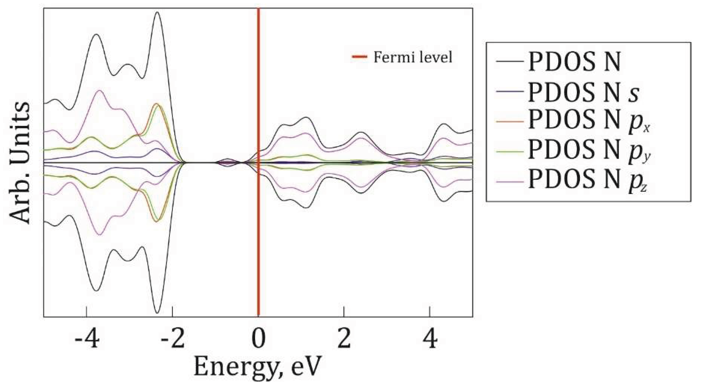
Orbital resolved PDOSes for carbon and nitrogen atoms are presented in Figure 8 and Figure 9, respectively to reveal the mechanism of chemical bond restructuring after the P-addition. The VB is mostly formed by N px and py orbitals at [-2.5; -2] eV region with a minor impact of carbon and N pz PDOSes. The [-5; -3] eV energy region is mostly formed by N pz states. The CB is equally defined by mostly pz orbitals of N and C. The impact of px and py orbitals of C and N at [0; 5] eV is minor. Also, it is fair to claim a minor impact of C and N PDOSes into a midgap state around -1eV, with a major impact of P states (Figure 6). The orbital analysis demonstrates the presence of hybridized px, py states, responsible for the formation of in-plane N-C and N-P σ-bonds, and dominant impact of pz-orbitals interactions, responsible for π-bond formation below and above the g-CN1 plane.
To estimate the charge redistribution and presence of hybridized px, py subsystem, the charge map was depicted and analyzed (Figure S3). The electronic charge is delocalized along entire P@g-CN1 lattice demonstrating a uniform charge distribution. The charge map additionally to DOS distribution analysis confirms delocalized nature of the electronic density and conjugate nature px and py electronic states described above.
4. Conclusion
Phosphorus doping has been demonstrated to be an effective strategy for tuning the structural and electronic properties of triazine-based graphitic carbon nitride. Both experimental observations and DFT calculations consistently show that phosphorus incorporation preserves the fundamental lattice topology while inducing local lattice relaxation, surface corrugation, and extended flake morphology—features that closely correspond to experimental TEM images, X-ray diffraction patterns, and photoluminescence spectra. The structural corrugation observed in TEM images of the P@g-CN1 composite can be rationalized in terms of the Topology Conservation Theorem. The introduction of phosphorus adatoms into the g-CN1 lattice leads to a marked suppression of charge recombination and a significant improvement in charge separation efficiency through flat bands formation. Electronic structure analysis reveals that phosphorus doping induces downward shifts of the valence and conduction bands and introduces localized midgap states near the Fermi level, thereby enhancing electronic delocalization and facilitating carrier transport. The resulting P@g-CN1 composite retains its semiconducting character with strong π–σ hybridization between carbon and nitrogen p orbitals. Good qualitative agreement between experimental spectroscopic and microscopic results and theoretical predictions highlights the strong complementarity of both approaches, providing a coherent atomic-scale understanding of bonding and electronic structure in phosphorus-doped g-C₃N₄. These findings not only elucidate the origin of the enhanced photocatalytic performance but also provide valuable guidelines for the rational design of efficient, metal-free two-dimensional photocatalysts and photovoltaic materials.
Supplementary Materials
The following supporting information can be downloaded at the website of this paper posted on Preprints.org.
Acknowledgments
This study was supported by the Ministry of Science and Higher Education of the Russian Federation, Project FSWM-2025-0007 (electronic structure calculations), and by the Fundamental Research Funds for the Central Universities of China, Project 2023FRFK06002 (result interpretation and manuscript preparation). Iu. M. gratefully acknowledges the Information Technology Centre of Novosibirsk State University for providing access to high-performance computing facilities. The authors also express their sincere gratitude to Prof. Chebli Derradji for his valuable discussions and insightful comments.
References
- Hu, J.; Hu, C.; Liu, H.; Jiao, F. Nitrogen Self-Doped Graphitic Carbon Nitride with Optimized Band Gap as a Visible-Light-Driven Photocatalyst for Hydrogen Production and Pollutant Degradation. Ind. Eng. Chem. Res. 2025, 64, 2696–2707. [Google Scholar] [CrossRef]
- Babu, P.; Park, H.; Park, J.Y. Surface chemistry of graphitic carbon nitride: doping and plasmonic effect, and photocatalytic applications. Surf. Sci. Technol. 2023, 1, 1–50. [Google Scholar] [CrossRef]
- Mottammal, D.; Cherusseri, J.; Thomas, S.A.; R. S., R.I.; Rajendran, D.N.; Choi, M.Y. Toward Doping in Graphitic Carbon Nitride: Progress and Perspectives on Catalytic Hydrogen Production. Adv. Mater. Technol. 2025, 10. [Google Scholar] [CrossRef]
- Zhang, W.; Xu, D.; Wang, F.; Chen, M. Element-doped graphitic carbon nitride: confirmation of doped elements and applications. Nanoscale Adv. 2021, 3, 4370–4387. [Google Scholar] [CrossRef] [PubMed]
- Jiang, L.; Yuan, X.; Pan, Y.; Liang, J.; Zeng, G.; Wu, Z.; Wang, H. Doping of graphitic carbon nitride for photocatalysis: A reveiw. Appl. Catal. B: Environ. 2017, 217, 388–406. [Google Scholar] [CrossRef]
- Meng, B.; Xiao, W.-Z.; Wang, L.-L.; Yue, L.; Zhang, S.; Zhang, H.-Y. Half-metallic and magnetic properties in nonmagnetic element embedded graphitic carbon nitride sheets. Phys. Chem. Chem. Phys. 2015, 17, 22136–22143. [Google Scholar] [CrossRef]
- Rono, N.; Kibet, J.K.; Martincigh, B.S.; Nyamori, V.O. A review of the current status of graphitic carbon nitride. Crit. Rev. Solid State Mater. Sci. 2020, 46, 189–217. [Google Scholar] [CrossRef]
- Yousefi, M.; Faraji, M.; Asgari, R.; Moshfegh, A.Z. Effect of boron and phosphorus codoping on the electronic and optical properties of graphitic carbon nitride monolayers: First-principle simulations. Phys. Rev. B 2018, 97, 195428. [Google Scholar] [CrossRef]
- Dong, G.; Zhang, Y.; Pan, Q.; Qiu, J. A fantastic graphitic carbon nitride (g-C3N4) material: Electronic structure, photocatalytic and photoelectronic properties. J. Photochem. Photobiol. C Photochem. Rev. 2014, 20, 33–50. [Google Scholar] [CrossRef]
- Babu, P.; Park, H.; Park, J.Y. Surface chemistry of graphitic carbon nitride: doping and plasmonic effect, and photocatalytic applications. Surf. Sci. Technol. 2023, 1, 1–50. [Google Scholar] [CrossRef]
- Starukh, H.; Praus, P. Doping of Graphitic Carbon Nitride with Non-Metal Elements and Its Applications in Photocatalysis. Catalysts 2020, 10, 1119. [Google Scholar] [CrossRef]
- Shevlin, S.A.; Guo, Z.X. Anionic Dopants for Improved Optical Absorption and Enhanced Photocatalytic Hydrogen Production in Graphitic Carbon Nitride. Chem. Mater. 2016, 28, 7250–7256. [Google Scholar] [CrossRef]
- Stolbov, S.; Zuluaga, S. Sulfur doping effects on the electronic and geometric structures of graphitic carbon nitride photocatalyst: insights from first principles. J. Physics: Condens. Matter 2013, 25, 085507. [Google Scholar] [CrossRef] [PubMed]
- Kesavan, G.; Sorescu, D.C.; Ahamed, R.; Damodaran, K.; Crawford, S.E.; Askari, F.; Star, A. Influence of gadolinium doping on structural, optical, and electronic properties of polymeric graphitic carbon nitride. RSC Adv. 2024, 14, 23342–23351. [Google Scholar] [CrossRef]
- Li, C.; Li, J.; Huang, Y.; Liu, J.; Ma, M.; Liu, K.; Zhao, C.; Wang, Z.; Qu, S.; Zhang, L.; et al. Recent development in electronic structure tuning of graphitic carbon nitride for highly efficient photocatalysis. J. Semicond. 2022, 43. [Google Scholar] [CrossRef]
- Dong, G.; Zhang, Y.; Pan, Q.; Qiu, J. A fantastic graphitic carbon nitride (g-C3N4) material: Electronic structure, photocatalytic and photoelectronic properties. J. Photochem. Photobiol. C Photochem. Rev. 2014, 20, 33–50. [Google Scholar] [CrossRef]
- Melchakova, I.; Nikolaeva, K.M.; Kovaleva, E.A.; Tomilin, F.N.; Ovchinnikov, S.G.; Tchaikovskaya, O.N.; Avramov, P.V.; Kuzubov, A.A. Potential energy surfaces of adsorption and migration of transition metal atoms on nanoporus materials: The case of nanoporus bigraphene and G-C3N4. Appl. Surf. Sci. 2021, 540. [Google Scholar] [CrossRef]
- Thomas, A.; Fischer, A.; Goettmann, F.; Antonietti, M.; Müller, J.-O.; Schlögl, R.; Carlsson, J.M. Graphitic carbon nitride materials: variation of structure and morphology and their use as metal-free catalysts. J. Mater. Chem. 2008, 18, 4893–4908. [Google Scholar] [CrossRef]
- Dong, G.; Zhang, Y.; Pan, Q.; Qiu, J. A fantastic graphitic carbon nitride (g-C3N4) material: Electronic structure, photocatalytic and photoelectronic properties. J. Photochem. Photobiol. C Photochem. Rev. 2014, 20, 33–50. [Google Scholar] [CrossRef]
- Avramov, P. Topology conservation theorem, quantum instability and violation of subperiodic symmetry of complex low-dimensional lattices. Acta Crystallogr. Sect. A Found. Adv. 2023, 79, C325–C325. [Google Scholar] [CrossRef]
- Avramov, P.V.; Kuklin, A.V. Topological and quantum stability of low-dimensional crystalline lattices with multiple nonequivalent sublattices. New J. Phys. 2022, 24, 103015. [Google Scholar] [CrossRef]
- Kresse, G.; Hafner, J. Ab initiomolecular dynamics for liquid metals. Phys. Rev. B 1993, 47, 558–561. [Google Scholar] [CrossRef] [PubMed]
- Kresse, G.; Hafner, J. Ab initiomolecular-dynamics simulation of the liquid-metal–amorphous-semiconductor transition in germanium. Phys. Rev. B 1994, 49, 14251–14269. [Google Scholar] [CrossRef] [PubMed]
- Kresse, G.; Furthmüller, J. Efficient iterative schemes forab initiototal-energy calculations using a plane-wave basis set. Phys. Rev. B 1996, 54, 11169–11186. [Google Scholar] [CrossRef] [PubMed]
- Hohenberg, P.; Kohn, W. Inhomogeneous Electron Gas. Phys. Rev. 1964, 136, B864–B871. [Google Scholar] [CrossRef]
- Kohn, W.; Sham, L.J. Self-consistent equations including exchange and correlation effects. Phys. Rev. 1965, 140, A1133–A1138. [Google Scholar] [CrossRef]
- Blöchl, P.E. Projector augmented-wave method. Phys. Rev. B 1994, 50, 17953–17979. [Google Scholar] [CrossRef]
- Kresse, G.; Joubert, D. From ultrasoft pseudopotentials to the projector augmented-wave method. Phys. Rev. B 1999, 59, 1758–1775. [Google Scholar] [CrossRef]
- Perdew, J.P.; Burke, K.; Ernzerhof, M. Generalized gradient approximation made simple. Phys. Rev. Lett. 1996, 77, 3865–3868. [Google Scholar] [CrossRef]
- Grimme, S. Semiempirical GGA-type density functional constructed with a long-range dispersion correction. J. Comput. Chem. 2006, 27, 1787–1799. [Google Scholar] [CrossRef]
- Yang, Z.; Xing, Z.; Feng, Q.; Jiang, H.; Zhang, J.; Xiao, Y.; Li, Z.; Chen, P.; Zhou, W. Sandwich-like mesoporous graphite-like carbon nitride (Meso-g-C3N4)/WP/Meso-g-C3N4 laminated heterojunctions solar-driven photocatalysts. J. Colloid Interface Sci. 2020, 568, 255–263. [Google Scholar] [CrossRef]
- Majdoub, M.; Anfar, Z.; Amedlous, A. Emerging Chemical Functionalization of g-C3N4: Covalent/Noncovalent Modifications and Applications. ACS Nano 2020, 14, 12390–12469. [Google Scholar] [CrossRef] [PubMed]
- Patnaik, S.; Martha, S.; Parida, K.M. An overview of the structural, textural and morphological modulations of g-C3N4towards photocatalytic hydrogen production. RSC Adv. 2016, 6, 46929–46951. [Google Scholar] [CrossRef]
- Ge, L.; Han, C.; Xiao, X.; Guo, L.; Li, Y. Enhanced visible light photocatalytic hydrogen evolution of sulfur-doped polymeric g-C3N4 photocatalysts. Mater. Res. Bull. 2013, 48, 3919–3925. [Google Scholar] [CrossRef]
- Sun, M.; Zhu, C.; Wei, S.; Chen, L.; Ji, H.; Su, T.; Qin, Z. Phosphorus-Doped Hollow Tubular g-C3N4 for Enhanced Photocatalytic CO2 Reduction. Materials 2023, 16, 6665. [Google Scholar] [CrossRef]
Figure 1.
Atomic structure of triazine g-C3N4 (g-CN1) lattice. The unit cell is indicated by rhombus. Carbon atoms are depicted in brown and nitrogen atoms are depicted in grey.
Figure 1.
Atomic structure of triazine g-C3N4 (g-CN1) lattice. The unit cell is indicated by rhombus. Carbon atoms are depicted in brown and nitrogen atoms are depicted in grey.
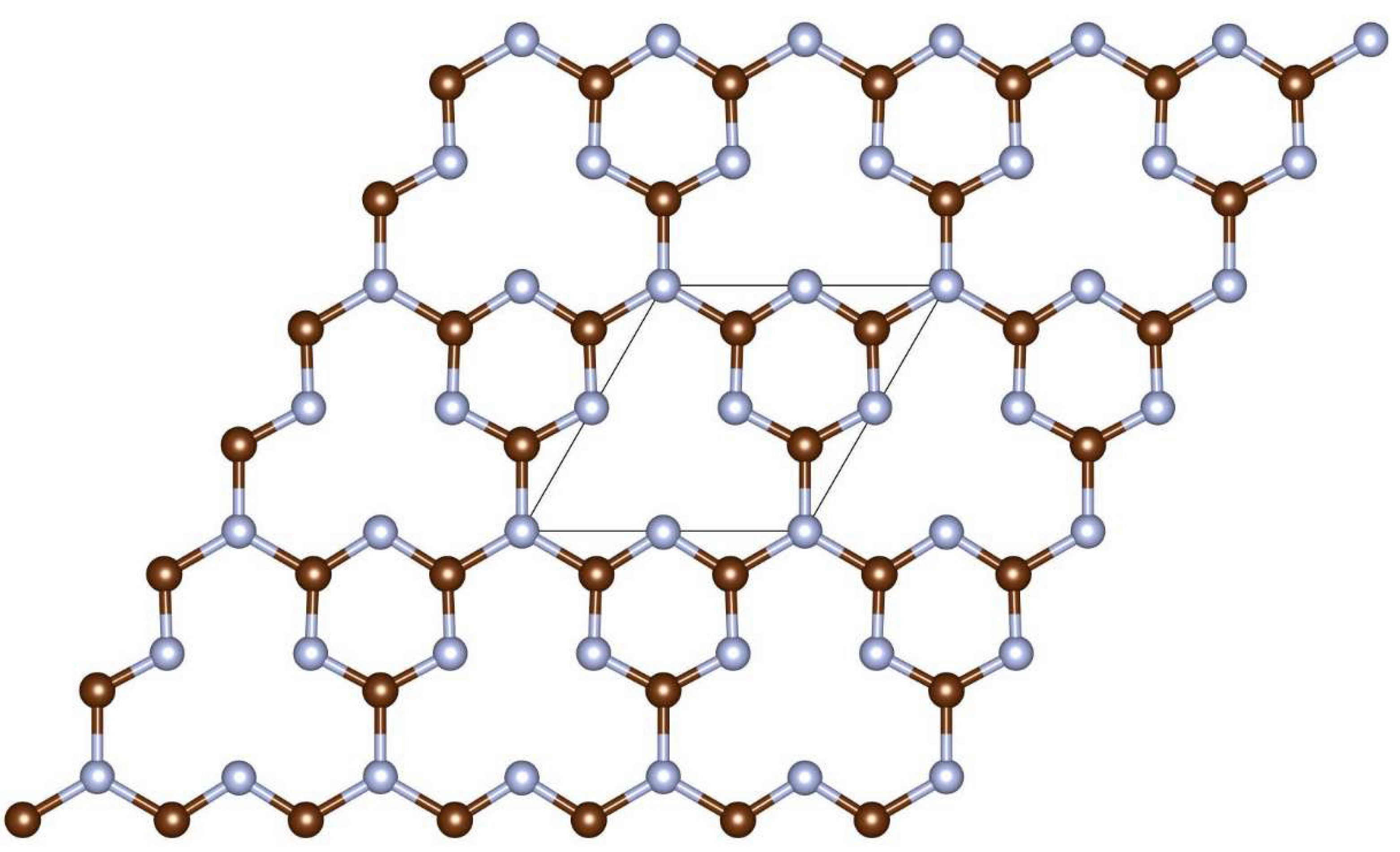
Figure 2.
P@g-CN1 lattice top view (left), side and diagonal (right). Carbon atoms are depicted in brown, nitrogen atoms are depicted in silver, and phosphorus atoms are depicted in gray. Unit cell is framed with the parallelogram.
Figure 2.
P@g-CN1 lattice top view (left), side and diagonal (right). Carbon atoms are depicted in brown, nitrogen atoms are depicted in silver, and phosphorus atoms are depicted in gray. Unit cell is framed with the parallelogram.
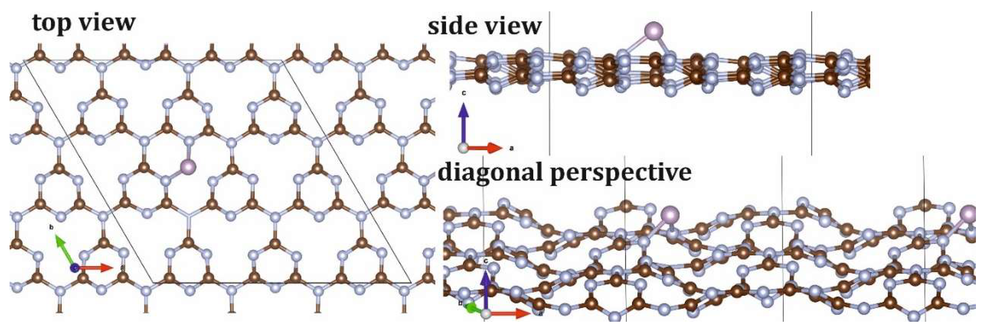
Figure 3.
TEM images of different samples g-CN1 (a) and (b), P@g-CN1 (c) and (d).
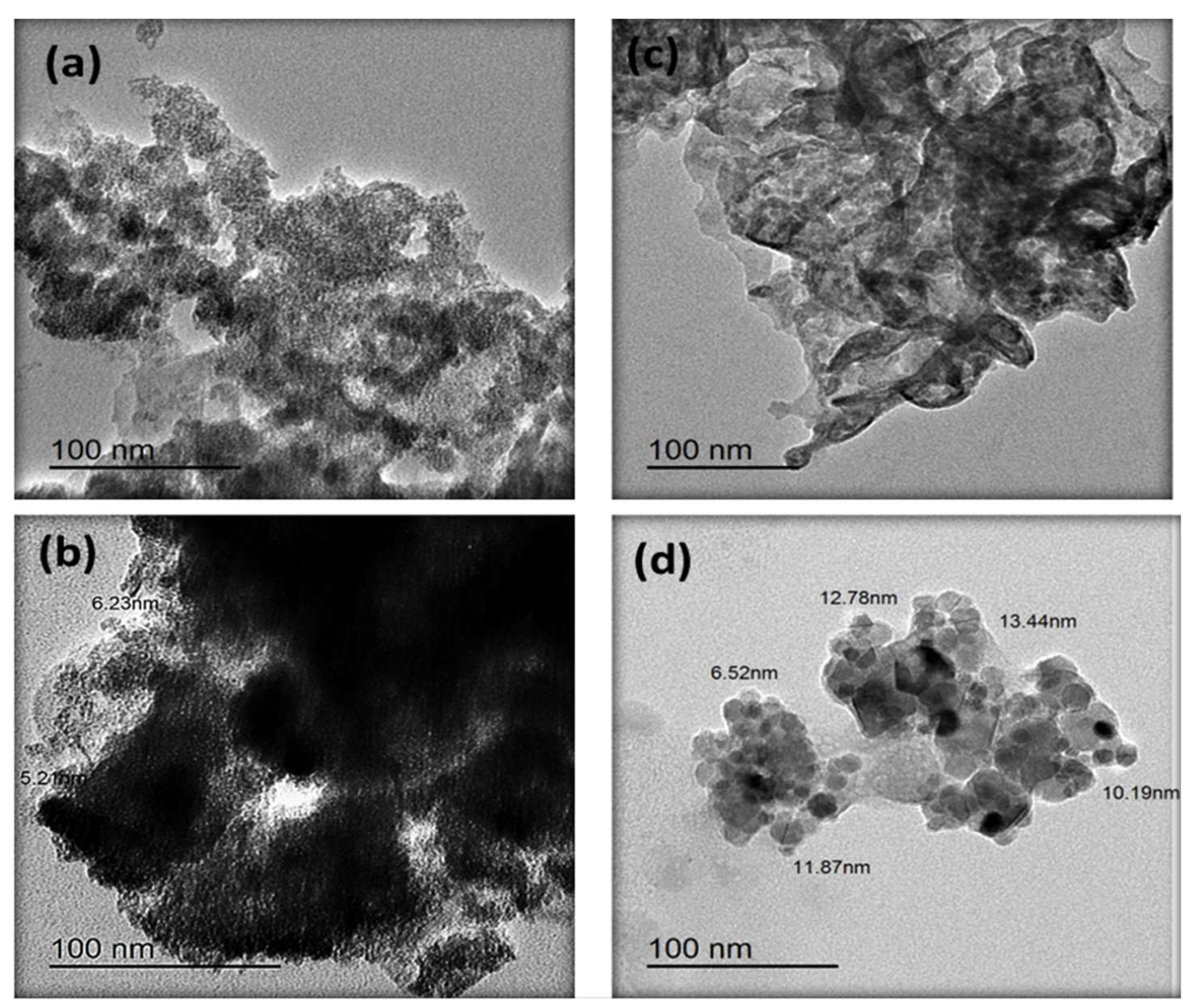
Figure 4.
a) X-ray diffraction patterns of parent pure g-C3N4 (black solid line) and P@g-C3N4 (red solid line). b) Photoluminescence spectra (arbitrary units) of parent pure g-C3N4 (black solid line) and P@g-C3N4 (blue solid line).
Figure 4.
a) X-ray diffraction patterns of parent pure g-C3N4 (black solid line) and P@g-C3N4 (red solid line). b) Photoluminescence spectra (arbitrary units) of parent pure g-C3N4 (black solid line) and P@g-C3N4 (blue solid line).
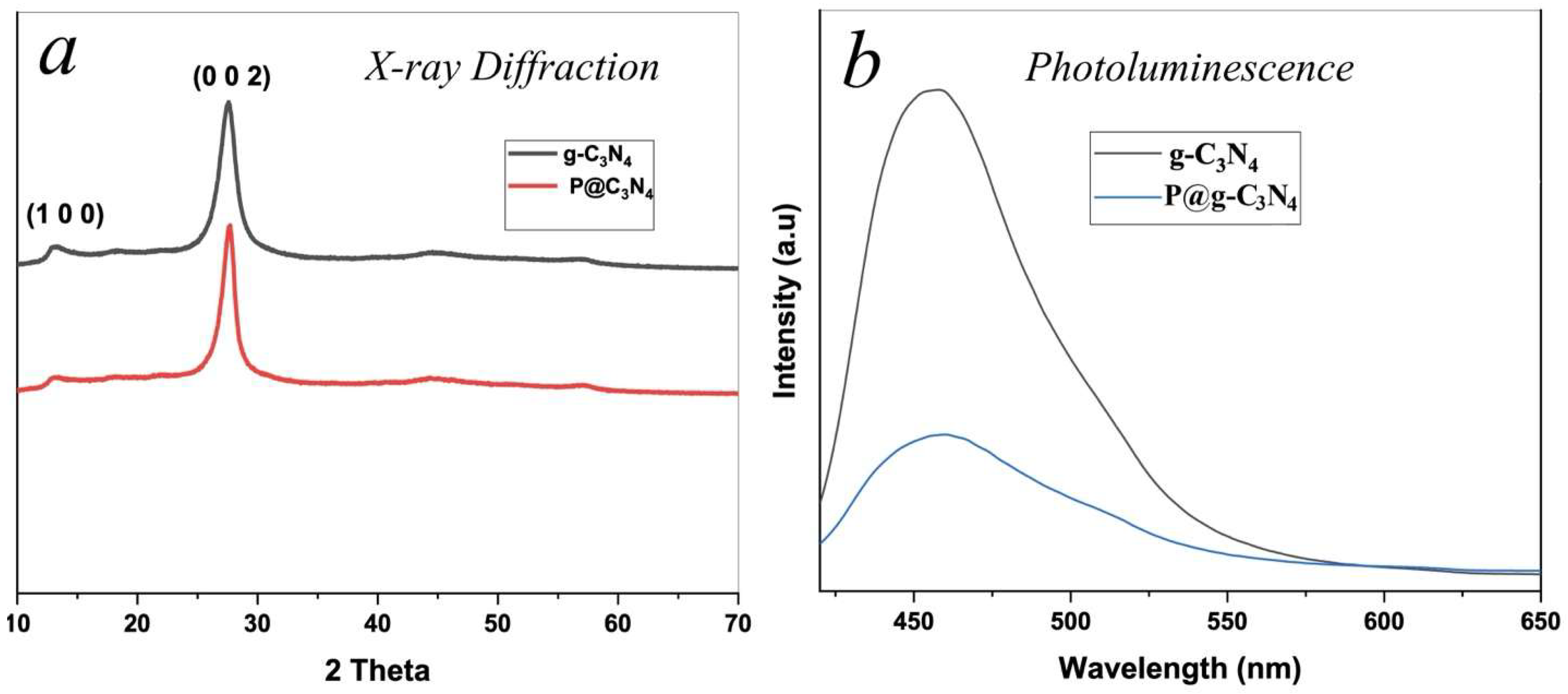
Figure 5.
Total density of states of free-standing g-CN1. The Fermi level in indicated as a red line at 0 eV.
Figure 5.
Total density of states of free-standing g-CN1. The Fermi level in indicated as a red line at 0 eV.
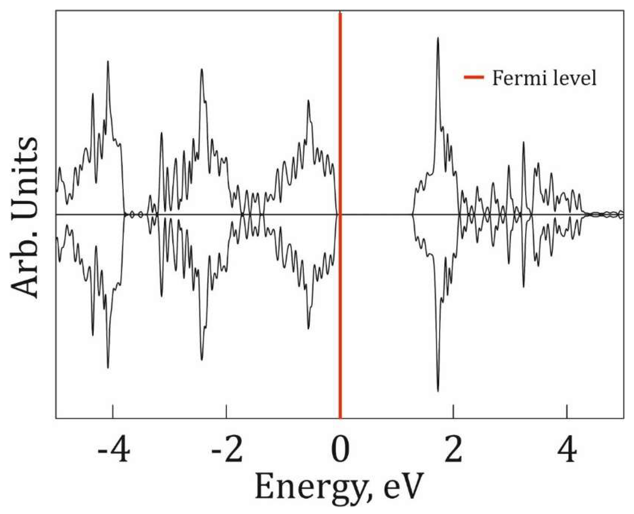
Figure 6.
Total and partial density of states of P@g-CN1 in both spin-up (positive) and spin-down (negative) channels. TDOSes are depicted by black solid lines, whereas PDOSes are depicted in red (carbon), blue (nitrogen), and green (phosphrus). The Fermi level is indicated by a red line at 0 eV.
Figure 6.
Total and partial density of states of P@g-CN1 in both spin-up (positive) and spin-down (negative) channels. TDOSes are depicted by black solid lines, whereas PDOSes are depicted in red (carbon), blue (nitrogen), and green (phosphrus). The Fermi level is indicated by a red line at 0 eV.
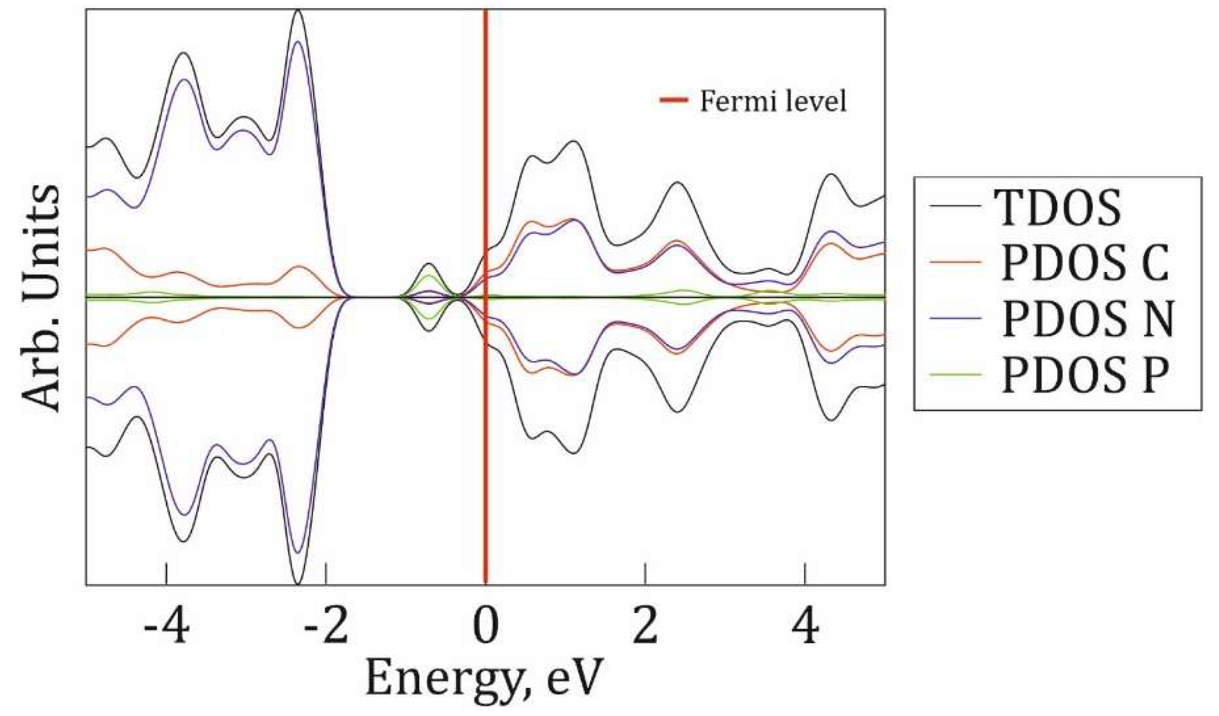
Figure 7.
The band structure of P@g-CN1 (left) and pristine g-CN1 (right). The Fermi level is indicated as a red line at 0 eV.
Figure 7.
The band structure of P@g-CN1 (left) and pristine g-CN1 (right). The Fermi level is indicated as a red line at 0 eV.
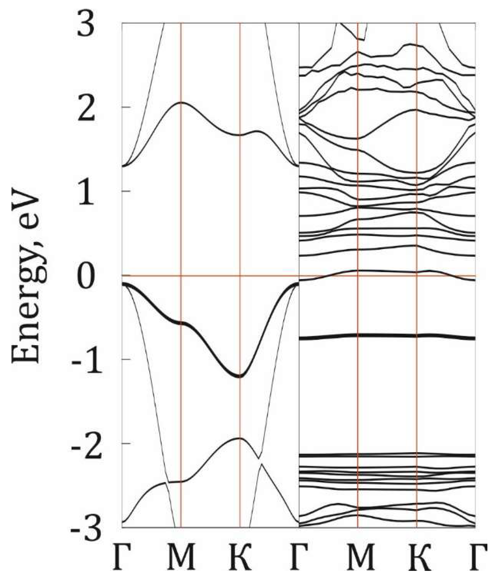
Figure 8.
P@g-CN1 integrated orbital resolved density of states of carbon atoms (PDOS C) is depicted in black, partial carbon s-orbital DOS (PDOS C s) is depicted in blue, partial carbon px-orbital (PDOS C px) is depicted in red, partial carbon py-orbital DOS (PDOS C py) is depicted in green, and partial carbon pz-orbital DOS (PDOS C pz) is depicted in purple. The Fermi level is indicated as a red line at 0 eV.
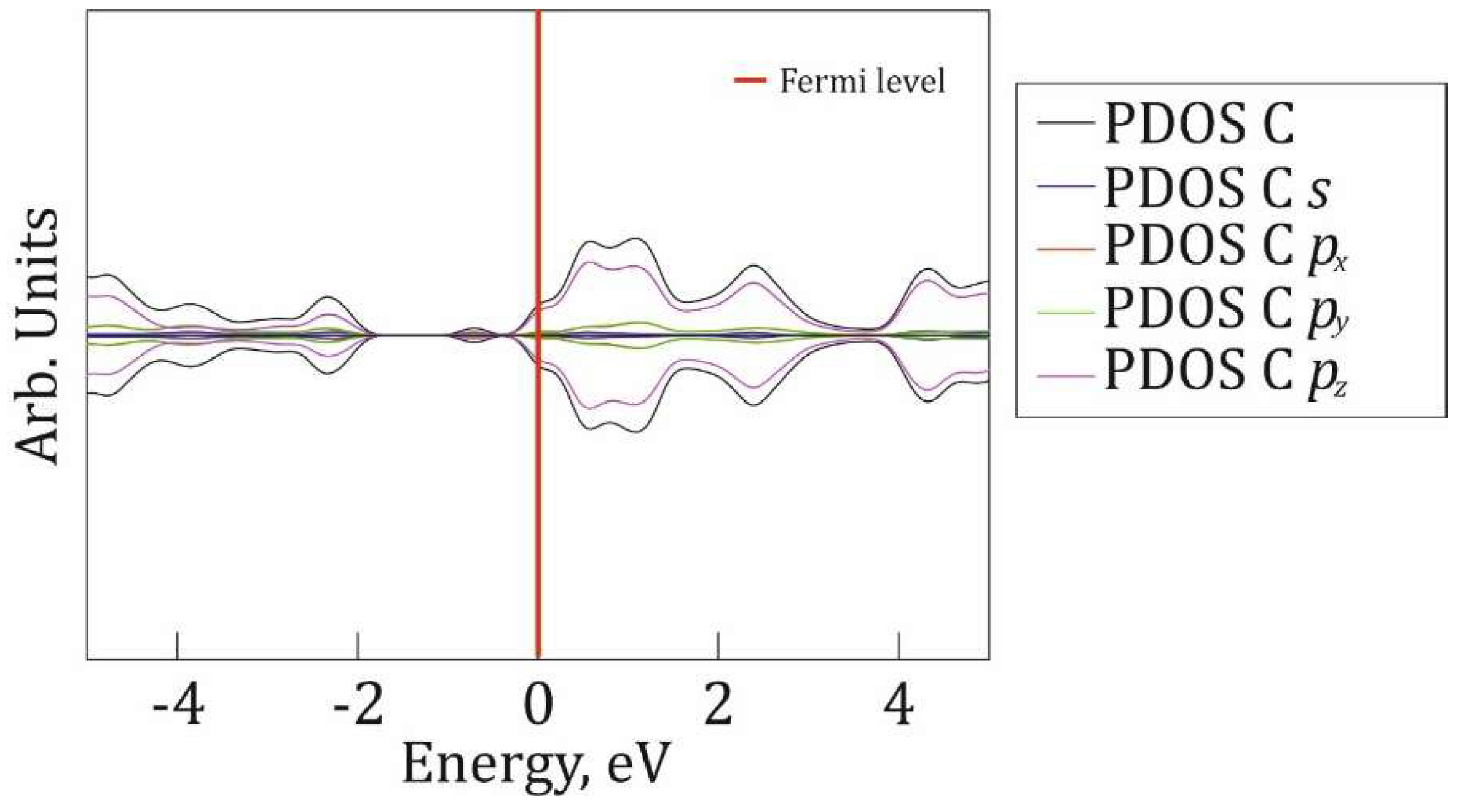
Figure 9.
P@g-CN1 integrated orbital resolved density of states of nitrogen atoms (PDOS N) is depicted in black, partial nitrogen s-orbital DOS (PDOS N s) is depicted in blue, partial nitrogen px-orbital (PDOS N px) is depicted in red, partial nitrogen py-orbital DOS (PDOS N py) is depicted in green, and partial nitrogen pz-orbital DOS (PDOS N pz) is depicted in purple. The Fermi level in indicated as a red line at 0 eV.
Disclaimer/Publisher’s Note: The statements, opinions and data contained in all publications are solely those of the individual author(s) and contributor(s) and not of MDPI and/or the editor(s). MDPI and/or the editor(s) disclaim responsibility for any injury to people or property resulting from any ideas, methods, instructions or products referred to in the content. |
© 2025 by the authors. Licensee MDPI, Basel, Switzerland. This article is an open access article distributed under the terms and conditions of the Creative Commons Attribution (CC BY) license (https://creativecommons.org/licenses/by/4.0/).
Copyright: This open access article is published under a Creative Commons CC BY 4.0 license, which permit the free download, distribution, and reuse, provided that the author and preprint are cited in any reuse.


