
Submitted:
21 November 2025
Posted:
21 November 2025
You are already at the latest version
Abstract
Laser slicing has emerged as a promising low-kerf and low-damage technique for fabricating SiC wafers; however, its influence on crystal integrity, near-surface modification, and charge-transport properties requires further clarification. In this study, a heavily N-doped 4° off-axis 4H-SiC wafer was sliced using a UV picosecond laser, and both the laser-irradiated surface and the laser-sliced (detached) surface were comprehensively characterized. X-ray diffraction and pole-figure measurements confirm that the 4H stacking sequence and macroscopic crystal orientation are preserved after slicing. Raman spectroscopy, including analysis of the folded transverse optical (FTO) mode and LO phonon–plasmon coupled (LOPC) modes, enabled dielectric-function fitting and determination of the plasmon frequency, yielding a free-carrier concentration of approximately 3.1 × 10¹⁸ cm⁻³. Hall measurements provide consistent carrier density, mobility, and resistivity, demonstrating that the laser slicing process does not degrade bulk electrical quality. Multi-scale AFM, angle-resolved XPS, SIMS, and TEM/SAED reveal the formation of a thin amorphous/polycrystalline modified layer and an oxygen-rich region confined to the near surface, with significantly increased roughness and thicker modified layers on the hill regions of the sliced surface. These results show that UV laser slicing maintains the intrinsic crystal and electrical properties of 4H-SiC while introducing localized nanoscale surface damage, which must be minimized through optimized slicing parameters and subsequent surface-finishing processes.
Keywords:
SiC wafer
; laser slicing
; ARXPS
; SIMS
; TEM
; surface damage
; crystal integrity
1. Introduction
Silicon carbide (SiC), a third-generation wide-bandgap semiconductor, has become the substrate of choice for power devices in applications such as electric-vehicle (EV) main-drive inverters [1], fast charging, grid-connected photovoltaics [2], and electric power transmission [3], owing to its high breakdown electric field, high thermal conductivity, and high carrier saturation drift velocity [4]. As global power-electronics capacity expands and automotive demand rises rapidly, there is an urgent need for SiC wafer-manufacturing technologies that deliver high yield, low cost, and low loss [5,6,7,8].
Conventional slicing methods, such as diamond-wire sawing, are prone to wafer fracture [9], kerf loss [10,11], and the introduction of surface damage (scratches and microcracks) and subsurface damage [12]. This not only wastes expensive raw materials but also necessitates time-consuming, labor-intensive post-polishing to meet epitaxial-growth surface requirements, further driving up overall cost. Compared with traditional diamond-wire cutting, laser slicing has emerged as a strong alternative for SiC wafer fabrication thanks to its potential for reduced kerf loss, thin-wafer capability, and suitability for hard and brittle materials [13,14,15,16,17]. Laser slicing utilizes high-intensity laser pulses to interact within the ingot, induces phase separation, point defects and dislocations, and microcracks, forming a thin damaged layer. Subsequent application of mechanical stress, thermal stress, or volumetric-expansion stress triggers interlayer delamination [18], thereby separating the damaged layer from the intact single-crystal region.
The machining performance of laser slicing is tightly governed by laser parameters: wavelength, pulse duration, single-pulse energy/fluence, repetition rate/burst structure, polarization, beam profile and numerical aperture/aberrations, as well as process-path parameters such as scan speed, pitch/step-over, and depth [19,20,21,22,23]. Together, these factors determine in-bulk absorption, modification thresholds, the continuity of the modified layer, and crack propagation paths. In recent years, many studies have focused on expanding and optimizing the process window. Zhang et al. used ultrafast lasers to create internal modified layers for wafer slicing and systematically examined how pulse duration, pulse energy, and scan speed/spacing/depth affect the modified-layer structure and exfoliation quality [24]. Lu et al., combining a weighted Gerchberg–Saxton (GSW) algorithm with spherical-aberration correction, generated dual-focus beams to achieve synchronous dual-layer cleaving in SiC, markedly improving slicing efficiency [25]. Yan et al. optimized the total energy and the number of sub-pulses in temporally shaped ultrafast pulse trains to precisely regulate carrier excitation near the focus, achieving a single modified layer only 16.5 μm thick and controlled cracking in semi-insulating SiC [26]. Liu et al. proposed an all-laser two-step method for slicing 4H-SiC, where high-fluence pulses pre-seed microcracks that are subsequently promoted and interconnected by low-fluence pulses, enabling wafer separation with low kerf loss and low surface roughness [27].
Localized laser focusing generates extreme temperature/pressure and ultrafast nonequilibrium dynamics, which introduce lattice disorder [28], subsurface defects [29,30,31], and chemical reconfiguration [32,33,34] in the near-surface/subsurface region of SiC. These changes can degrade subsequent chemical–mechanical polishing (CMP), epitaxial growth, device integrity, and electrical performance. Prior studies using SEM, TEM/SAED [35,36,37], Raman spectroscopy [38,39,40], XRD [41], AFM [42], XPS [43] have observed amorphous/nanocrystalline layers of varying thickness and microcrack networks adjacent to the laser-modified region, accompanied by surface/near-surface oxidation, adventitious contamination, or valence-state rearrangement. Such structural and chemical non-idealities require post-processing for repair and passivation [44]. Plasma-based remediation, high-temperature hydrogen etching (hydrogen anneal), sacrificial oxidation followed by oxide removal, and fine CMP have all been shown to reduce subsurface damage, improve roughness, and lower interface state density, thereby providing a cleaner surface for subsequent epitaxy and gate dielectric formation [45,46,47]. Recent work further suggests that multi-step plasma schemes [48] can synergistically heal residual defects left after CMP, earlier studies also demonstrate that hydrogen etching [49,50] and sacrificial oxidation [51,52,53,54] can controllably tune the surface morphology and composition of 4H-SiC—experience that is equally instructive for post-separation surface/interface reconditioning after laser slicing.
At present, an in-depth understanding of the microstructural evolution, chemical-composition gradients, and their associated physical properties at laser-separated surfaces remains incomplete—yet such knowledge is essential for assessing the true manufacturability of this technique and for designing effective post-processing repair strategies. Motivated by this gap, the present work conducts a systematic investigation of surface modifications on SiC wafers after laser slicing. Using a suite of complementary techniques, we directly compare the original polished face with the laser-separated face. By integrating X-ray diffraction (XRD), micro-Raman spectroscopy, angle-resolved X-ray photoelectron spectroscopy (ARXPS), secondary ion mass spectrometry (SIMS), scanning electron microscopy (SEM), atomic force microscopy (AFM), four-point-probe electrical measurements, and cross-sectional transmission electron microscopy (TEM), we achieve an analysis that spans from the atomic to the micron scale. We quantitatively evaluate laser-induced differences in structural disorder, subsurface defects, chemical valence states, and surface roughness, elucidate their implications for electrical performance and interfacial quality, and discuss viable post-treatment pathways to enable high-quality SiC wafer manufacturing.
2. Experimental Method
2.1. The Laser System
A pulsed ultraviolet (UV) laser system with a wavelength of 365 nm was employed for the slicing experiments. The laser operated with a pulse duration (τ) of 10 ps and a repetition rate (f) of 100 kHz, allowing precise control of energy delivery. Each pulse possessed an energy (E) of 0.30 μJ, focused to a spot diameter (1/e²) of approximately 8 μm. The corresponding peak intensity and fluence were 1.2 × 10² GW cm⁻² and 1.2 J cm⁻², respectively, as calibrated using a power meter and knife-edge method. During processing, the laser beam was scanned at a speed (v) of 40 mm s⁻¹. The laser polarization was linear, oriented at 90° relative to the scan direction, and all experiments were conducted under a nitrogen-purged atmosphere (flow rate: 5–10 L min⁻¹) to suppress oxidation during irradiation. A comparison of the laser parameters used in this study with those reported in previous works is provided in Table S1, illustrating how our experimental conditions relate to those used in similar slicing experiments.
2.2. Materials and Characterization
The starting N-doped 4H-SiC material is a 4° off-axis n-type single-crystal substrate with a doping concentration of 1 × 1018 cm−3 by nitrogen. Single-crystalline 4H-SiC ingots were subjected to laser slicing using a pulsed ultraviolet laser system (λ = 365 nm) with controlled pulse width and repetition rate to achieve precise separation. The resulting wafer (~120 μm thick) was divided into front (laser-irradiated) and back (laser-sliced) regions for comparison. X-ray diffraction (XRD), micro-Raman spectroscopy, SEM/EDS, AFM, ARXPS, SIMS, four-point probe measurements, and FIB-TEM/EDS analyses were conducted as described previously. A JEOL JSM-IT800 scanning electron microscope (SEM) (operating conditions: accelerating voltage: 15.0 kV, probe current: 5 nA, working distance: 10 mm) was used to observe microscale surface features such as the recast layer, spatter, edge burrs, and microcracks. High-resolution secondary-electron images were acquired. Energy-dispersive X-ray spectroscopy (EDS) integrated into the JEOL JSM-IT800 SEM (energy resolution 127 eV @ 130,000 cps) was used for elemental point analyses and area mapping, to obtain semi-quantitative atomic percentages for Si, C, O, N (operating conditions: accelerating voltage: 15.0 kV, probe current: 5 nA, working distance: 10 mm). A Seiko Instruments SPA-400 atomic force microscope (AFM), operating in tapping mode (lateral resolution: 0.2 nm, vertical resolution: 0.01 nm, scan range: XY 20 µm, Z 1 µm), was employed to scan the surface and obtain three-dimensional topography as well as quantitative roughness parameters—arithmetic mean roughness (Ra) and root-mean-square roughness (Rrms), to assess nanoscale undulations induced by laser processing. XRD measurements were carried out on an XPERT-PRO diffractometer (goniometer PW3050/65). A monochromated Cu Kα1 radiation was used (λ = 1.5406 Å). XRD served to identify the bulk crystal structure and to detect any new phases potentially induced by laser machining. Raman spectra were measured under 532 nm excitation using a Raman spectrometer (Horiba, LabRam, HR 800) to characterize laser-induced disordered/graphitic-like carbon, the defect density was quantified from the D/G intensity ratio (ID/IG). 20 × 20 µm2 maps were acquired on both the laser-irradiated surface and laser-sliced surface, and—besides the carbon bands at ~1350 and ~1580 cm⁻¹—the 4H-SiC folded transverse optic (FTO(1/2)) mode near ~777 cm⁻¹ was mapped to assess the substrate crystallinity. To analyze the laser-sliced SiC damage layer, recast layer, and their nanoscale structure and local chemistry relative to the polished surface, cross-sectional lamellae were prepared by focused ion beam (FIB) using a Thermo Scientific Helios 5 UX system (operating conditions: 3 kV, 0.40 nA probe current, 12,000× magnification, working distance: 4.0 mm, horizontal field width: 10.6 µm) and subjected to combined Thermo Fisher Talos F200X transmission electron microscopy (TEM), selected-area electron diffraction (SAED), and energy-dispersive X-ray spectroscopy (EDS). TEM imaging was performed at 200 kV in HAADF-STEM mode. SAED patterns were collected to index plane families and to evaluate crystalline and orientation dispersion. EDS conducted point, line, and area mappings focused on the spatial distributions of Si, C, O, and N across the surface and the transition zone.
For non-destructive information on surface chemical states and their depth distribution, ARXPS measurements were carried out on a Thermo Fisher Theta Probe AR-XPS System (monochromated Al Kα, hv = 1486.6 eV). The operating conditions were 15 kV, 100 W X-ray energy, with a 400 µm spot size. The photoelectron take-off angle was varied from 28° to 78° relative to the surface normal to control the effective probing depth. Core-level spectra of C 1s, O 1s, N 1s, and Si 2p were recorded, with energy referencing to C–C at 284.6 eV. Relative peak areas and their angular dependences were used to determine the vertical stratification of chemical components (such as C–C, C–Si, C–O, Si–O, and N-containing functionalities). Elemental depth profiling was performed using a CAMECA Magnetic Sector SIMS 7f-auto secondary ion mass spectrometer (SIMS) with a 7.5 keV O₂⁺ primary ion beam for sputtering and analysis, using a current of 20 nA and an analysis area of 250 × 250 µm2. The detected ions included 12C⁺ and 30Si⁺. For depth profiling, the same instrument was operated with a Cs⁺ primary ion source at 15.0 keV and 150 nA. A raster size of 150 × 150 μm2 was used with an analysis area of 30 μm in diameter, and the detected ions included ¹²C⁻, ¹²C¹⁴N⁻, ²⁸Si⁻ and ¹⁸O⁻. Hall effect and resistivity measurements were performed at room temperature using an Ecopia HMS 3000 Ver. 3.1 four-point probe system in accordance with the Van der Pauw method. The samples were mounted on a spring-clip board, and a constant current of 100 μA was applied while recording the Hall voltage. Bulk and sheet carrier concentrations, electrical conductivity, sheet resistance, electron mobility, and Hall coefficient were determined using the instrument’s built-in analysis software.
3. Results and Discussion
The fabrication process of the laser-sliced SiC wafer is illustrated in Figure 1. A high-purity 4H–SiC single-crystal ingot grown by physical vapor transport (PVT) was used as the starting material. The ingot was oriented along the [0001] c-axis and subsequently polished with a 4° off-cut toward the ⟨11-20⟩ direction to promote step-flow epitaxial growth and minimize the formation of micropipes or polytype inclusions. A pulsed ultraviolet laser (λ = 365 nm, τ ≈ 10 ps) was employed to locally modify the crystal beneath the wafer surface. The laser beam was tightly focused at a predetermined focal depth (~120 µm) inside the SiC bulk. By scanning the laser beam laterally across the surface while maintaining a constant focal plane, a periodic subsurface structure—known as a laser-modified layer—was formed. The pulse energy and repetition rate were carefully tuned to ensure localized melting or micro-decomposition without causing macroscopic cracking. The complete set of processing parameters used in this work, together with representative conditions from earlier SiC laser-processing studies (covering UV–NIR wavelengths, ps–ns pulse widths, different scan strategies, atmospheres, and fluence ranges), is summarized in Table S1, providing context for the specific processing window realized here. After laser processing, a mechanical or thermal stress gradient was applied along the irradiated region. The energy concentration and defect accumulation at the laser-modified interface induced cleavage along the processed plane, allowing the wafer to be spontaneously separated from the bulk crystal without the need for conventional wire-saw slicing. The detached wafer retained the same crystallographic orientation as the parent ingot and exhibited atomically flat terraces corresponding to the 4° off-cut angle. This method effectively minimizes kerf loss, reduces surface subsurface damage, and enables high-throughput, high-yield SiC wafer fabrication. Moreover, the laser slicing process is compatible with subsequent polishing or epitaxial growth steps, making it a promising approach for next-generation semiconductor manufacturing. For the as-obtained wafer, the surface facing the incoming beam is referred to as the wafer front side (laser-irradiated), whereas the surface corresponding to the separation plane is referred to as the wafer back side (laser-sliced). Then these two sides were used for the next characterization. To further illustrate the distinct characteristics of the laser-irradiated and laser-sliced surfaces, Figure S1 presents photographs of the 8-inch N-doped 4H-SiC wafer after laser slicing. The two sides of the laser-sliced 4H-SiC wafer exhibit distinct morphologies due to the different mechanisms involved in the laser-based separation process. The laser-irradiated side was directly exposed to the scanning laser during the slicing process. Localized thermal accumulation and stress concentration produced periodic trace-like surface textures and directional patterns characteristic of laser–matter interactions. As a result, this surface appears rougher and displays visible laser-track patterns. In contrast, the laser-sliced side represents the natural fracture plane formed at the focal depth of the ultraviolet laser (~120 μm). Because separation occurs internally without mechanical abrasion, this surface shows a relatively smooth morphology with minimal kerf loss or mechanical damage. This comparison clearly demonstrates how laser-induced internal cracking and surface irradiation contribute differently to the final wafer surface characteristics.
3.1. Surface Morphology
Figure 2 compares the surface morphologies and EDS results of the laser-irradiated and laser-sliced SiC surfaces. Figure 2a–c corresponds to the laser-irradiated side, whereas Figure 2d–f corresponds to the laser-sliced side. Low-magnification SEM image of the laser-irradiated surface (Figure 2a) shows periodic laser irradiated tracks with a spacing of 203 μm, where each track consists of a relatively smooth irradiated region surrounded by recast ridges. Figure 2b is a higher-magnification image of region “1” in Figure 2a, revealing excellent flatness with only extremely fine processing traces which came from the polishing process. Figure 2c shows a higher-magnification view of the cutting edge on the laser-irradiated surface (region “2” in Figure 2a), along the groove direction, regular and continuous wrinkle ripple-like protrusions with a uniform pitch are observed, and slight buildup and step features appear at the edges, merging into a single recast ridge. Owing to the local high temperature under laser irradiation, the surface undergoes rapid heating, melting, and vaporization decomposition, after which the molten and evaporated material rapidly solidifies, creating a recast layer at the cutting edges and across the surface. Figure 2d provides a low-magnification overview of the laser-sliced surface with a cutting-line pitch of 205 μm. Figure 2e and Figure 2f are higher-magnification images of regions “3” and “4” in Figure 2d, respectively. In Figure 2e, fine textures attributable to thermo-mechanical loading are evident. As shown in Figure 2f, compared with the laser-irradiated surface, through-thickness voids and cracks together with lamellar spallation can be observed, and the previously continuous ripples are disrupted. The high energy density of the laser rapidly heats the cutting region to extremely high temperatures, while diffusion and convection effects near the focal point create a strong temperature gradient within the material. This results in a thermal expansion mismatch between the recast layer and the SiC substrate, with the resulting thermal stresses further promoting the formation and propagation of microcracks at the interface [36]. The SiC wafer is thereby detached, leaving lamellar flakes and void features on the laser-cut surface. EDS analyses were performed on representative regions of the laser-irradiated surface (Figure 2g) and the laser-sliced surface (Figure 2h). Both spectra are dominated by Si with C from the SiC matrix, and the quantified elemental compositions for the two regions are summarized in Table S2. The laser-irradiated surface shows a trace O contribution, this is because mechanical abrasion during polishing exposes numerous unsaturated dangling bonds on the SiC surface [5,55]. These highly reactive sites subsequently react with oxygen (originating from O₂ or H₂O in the polishing medium or ambient air), thereby forming an increased amount of Si–O bonds. Meanwhile, the high temperatures and rapid solidification in the laser-incident region lead to some oxidation reactions, resulting in the formation of Si–O bonds on the laser-irradiated surface. In contrast, the laser-sliced surface, which is detached directly from the SiC wafer’s interior, is exposed to a much lower amount of oxygen during the cutting process. Since it has limited interaction with oxygen molecules when compared to the laser-irradiated region, consequently, the formation of oxygen-related components is strongly suppressed, and Table S2 confirms that no significant O content is detected on this side.
3.2. Surface Roughness
The surface morphology and roughness of the laser-irradiated surface and laser-sliced surface were analyzed using Atomic Force Microscopy (AFM). The SEM images in Figure 3a and Figure 3b provide an overview of the surface features of the laser-irradiated and laser-sliced sides, respectively. Figure 3a shows the laser-irradiated surface of the SiC sample, which is relatively flat and uniform, with AFM scan regions marked as “1” (black square) and “2” (yellow square). Figure 3b shows the laser-sliced surface, which exhibits more pronounced surface features, including hills and valleys, with AFM regions marked as “3” (red square, hill) and “4” (blue square, valley). Figure 3c–e presents the AFM 2D morphology of the laser-irradiated surface in regions 1 and 2. The scan areas are 20 × 20 μm² for Figure 3c and Figure 3d, and 1 × 1 μm² for Figure 3e. Overall, the 2D maps reveal a relatively flat surface with only small-amplitude undulations. The corresponding 3D topography images are shown in Figure 3f–h. The arithmetic mean roughness (Ra) and root-mean-square roughness (Rrms) were extracted from the AFM height data. Ra represents the mean absolute deviation from the average height, whereas Rrms is more sensitive to large height excursions due to its square-averaging definition. In region 1 (20 × 20 μm², Figure 3f), the surface exhibits long-wavelength waviness associated with polishing/processing marks, giving an occasional high average roughness of Ra ≈ 118 nm and a root-mean-square roughness of Rrms ≈ 162 nm. This large Rrms value reflects the presence of larger-scale roughness features (polishing streaks and machining marks) that are more pronounced than the average height deviations captured by Ra. In contrast, region 2, which is farther from the cutting traces, has a much flatter morphology, the 20 × 20 μm² scan (Figure 3g) yields Ra ≈ 1.56 nm and Rrms ≈ 2.15 nm, while the 1 × 1 μm² scan (Figure 3h) shows only nanoscale height fluctuations with Ra ≈ 0.47 nm and Rrms ≈ 0.63 nm, indicating that the locally polished terrace still maintains an atomically smooth surface at the sub-micrometer scale. Figure 3i–l shows the AFM 2D morphology of the laser-sliced SiC surface from the hill (region 3) and valley (region 4) areas. The scan areas are again 20 × 20 μm² for Figure 3i and Figure 3k, and 1 × 1 μm² for Figure 3j and Figure 3l. The corresponding 3D topography images and roughness values are summarized in Figure 3m–p. In the hill region, the 20 × 20 μm² scan (Figure 3m) reveals a strongly corrugated topography composed of ridges and grooves, with Ra ≈ 66 nm and Rrms ≈ 83 nm, indicating pronounced height fluctuations and a thick recast layer produced by laser cutting. When the scan size is reduced to 1 × 1 μm² (Figure 3n), the surface still shows distinct nanoscale protrusions and depressions, with Ra ≈ 8.6 nm and Rrms ≈ 3.4 nm, evidencing substantial local melting, rapid resolidification and microcrack-related roughening. In contrast, the valley region is relatively smoother. For the 20 × 20 μm² scan (Figure 3o), the roughness values are Ra ≈ 2.4 nm and Rrms ≈ 1.4 nm, while the 1 × 1 μm² scan (Figure 3p) yields Ra ≈ 0.44 nm and Rrms ≈ 0.56 nm. Although the valleys are rougher than the laser-irradiated smooth surface, their roughness is much lower than that of the hill regions, indicating that material removal and crack opening predominantly occur in the hills, whereas the valleys retain a comparatively flat morphology. The Ra and Rrms values demonstrate that the laser-irradiated surface maintains low roughness and uniform surface characteristic, while the laser-sliced surface exhibits a highly heterogeneous topography with very rough recast ridges, moderately rough hill areas at the nanoscale, and relatively smooth valley. These differences indicate that laser cutting induces strong localized thermal effects, leading to rapid solidification, splatter deposition and local cracking, which in turn generate irregular surface undulations and uneven roughness. The results highlight that optimization of laser parameters is necessary to suppress excessive hill formation and microcrack development, thereby improving the quality of the cut surface.
Figure S2 presents comprehensive line-profile plots obtained from various regions of the 4H-SiC wafer. The measured areas include (i) the laser-irradiated region, (ii) the non-irradiated region on the same laser-irradiated side, and (iii) the hill and valley regions formed on the laser-sliced side. Each location was scanned at two different magnifications (20 × 20 μm² and 1 × 1 μm²) to evaluate both large-scale roughness features and nanoscale surface textures. The height-profile plot corresponding to each AFM image provides quantitative roughness information extracted along with the indicated lateral scan trace. For laser-irradiated region (20 × 20 μm²), the AFM topography of the laser-irradiated region reveals pronounced and periodically aligned surface protrusions produced during the surface scanning of the UV laser. These features correspond to the laser-induced hill–valley texture, which arises from localized thermal accumulation, partial re-melting, and rapid quenching. The height profile confirms a large vertical variation, with peak-to-valley amplitudes approaching several hundred nanometers, consistent with strong laser–matter interaction at the surface. For non-irradiated region on the laser-irradiated side (20 × 20 μm² and 1 × 1 μm²), Despite being located on the laser-irradiated side, the non-irradiated region exhibits significantly lower roughness, as it was not directly exposed to the scanning beam. The AFM images show a relatively featureless surface with fine asperities typical of polished SiC substrates. The line profiles reveal small height fluctuations on the order of a few nanometers, indicating minimal thermal damage or mechanical disturbance beyond the laser-scanned tracks. For hill region on the laser-sliced side (20 × 20 μm² and 1 × 1 μm²), the hill regions on the laser-sliced side represent the upper portions of the fracture morphology generated during internal laser-induced cleaving. The AFM topography displays upwardly elevated features associated with the crack-propagation front. The roughness is moderate compared with the laser-irradiated surface but notably higher than the valley regions. Height profiles indicate peak-to-valley variations typically ranging from tens to hundreds of nanometers, reflecting local stress-release patterns at the fracture interface. iv) For valley region on the laser-sliced side (20 × 20 μm² and 1 × 1 μm²), in contrast to the hill regions, the valley regions show a remarkably smoother morphology. This smoother topology corresponds to the natural fracture plane created at the laser focal depth (~120 μm), where internal micro-cracking occurs with minimal thermal input. AFM results reveal small-scale height variations, often below several nanometers in the 1 × 1 μm² scans. These features validate that the valley regions retain the intrinsic atomic-scale cleavage characteristics of 4H-SiC with negligible kerf loss or mechanical abrasion.
3.3. Structural Phase Transformation
The diffraction pattern in Figure 4a shows two dominant peaks indexed as (0004) and (0008), corresponding to the 4H–SiC polytype. No additional peaks (e.g., (10-14), (11-28)) are observed, confirming that the wafer surface is perfectly aligned with the (0001) basal plane, and that the growth is epitaxially oriented along the c-axis. The sharpness and intensity of the (0004) reflection indicate a high degree of crystallinity and minimal defect density. The inset in Figure 4a shows the φ-scan around the (0004) plane. A single peak at φ ≈ 0° and –180° indicates no rotational twin or grain misalignment, confirming single-domain orientation over the measured area. This result suggests that the wafer surface was well polished and that the off-axis cut did not introduce noticeable in-plane distortions. The ω-scan of the (0004) reflection Figure 4b reveals a narrow FWHM of 138 arcsec (≈ 0.038°). This small rocking width indicates low mosaicity, implying that the lattice planes are nearly parallel over the X-ray illuminated region. Such narrow width is characteristic of high-quality single-crystal 4H–SiC substrates, typically used for epitaxial growth or laser-slicing experiments. The inset pole figure in Figure 4b displays a single intensity maximum at x = 0°, consistent with a perfect (0001) orientation. No secondary lobes or ring-shaped features are observed, confirming that no tilted grains or misoriented domains exist. The rocking curve FWHM (Δω = ±0.038°) corresponds to the angular width of the intensity distribution in the pole figure, quantitatively linking ω-scan mosaic spread and χ-tilt distribution.
The Raman spectrum (Figure 4c) measured from the 4H-SiC crystal clearly reveals both the zone-folded phonon modes characteristic of the polytype structure and the longitudinal optical phonon–plasmon coupled (LOPC) modes, enabling nondestructive evaluation of its structural and electrical properties. The 4H-SiC polytype consists of Si–C bilayers stacked with a periodicity of n = 4, forming a natural superlattice. The presence of folded phonon modes, such as the folded transverse optical (FTO) mode observed near 777 cm⁻¹, confirms the n = 4 stacking sequence of the 4H-SiC structure. It is important to note that these Raman peaks shown in the spectra were observed from regions of the laser-irradiated surface that are away from the laser-irradiated track, specifically excluding the areas around the ridge lines, where no peaks were detected. To assess its electrical properties, the LOPC modes at the Γ point—arising from the coupling between the LO phonon and free-carrier plasmon—were analyzed. The plasmon frequency (ωₚ), which represents the collective oscillation frequency of free electrons, is a key physical parameter for extracting the carrier concentration (n) through LOPC analysis. By examining the position and line shape of the LOPC features in the Raman spectrum and fitting them using a dielectric function model ε(ω) [56], the plasmon frequency ωₚ was obtained.
The corresponding free-carrier concentration was then calculated using the standard plasmon relation.
The analysis determined that the 4H-SiC sample possesses a carrier concentration of n = 3.1 × 10¹⁸ cm⁻³, demonstrating that Raman-based LOPC fitting provides an accurate, fully nondestructive approach for evaluating the electrical properties of wide-bandgap semiconductors. In addition, the results confirm that 4H-SiC exhibits lower crystallographic anisotropy compared with 6H-SiC, resulting in correspondingly weaker anisotropic effects in its LOPC behavior.
For a clearer visualization of these Raman modes, Figure S3 presents the Raman spectra and the corresponding two-dimensional intensity maps of characteristic vibrational modes obtained from the laser-irradiated surface of the 4H-SiC wafer. The Raman intensity maps of the irradiated region show pronounced spatial contrast, particularly in the 776 cm⁻¹ FTO mode, which exhibits strong, periodic intensity enhancement aligned with the laser-scan direction. This pattern directly correlates with the hill–valley surface morphology observed in optical and AFM images and indicates, i) localized modification of the stacking order ii) periodic strain accumulation along irradiated lines iii) slight lattice relaxation or deformation from thermal gradients. The 204 cm⁻¹ and 978 cm⁻¹ modes also display non-uniform distributions, though with subtler contrasts, confirming multiscale perturbation of the SiC lattice due to local heating and rapid cooling during laser exposure. Importantly, the 1522 cm⁻¹ G-band is selectively enhanced in the irradiated region, suggesting the presence of i) laser-induced carbonization, ii) defect-mediated Si–C bond breaking, iii) trace graphitic residues embedded at or near the surface. Such carbon-related features commonly arise in high-fluence laser interactions with SiC and act as chemical indicators of localized decomposition. Raman mapping of the non-irradiated region: The non-irradiated region displays markedly different Raman characteristics, i) all four Raman modes appear uniform and low in intensity, showing minimal variation over the scanned area. ii) the FTO mode at 776 cm⁻¹ appears consistent with an undamaged 4H-SiC surface, indicating no structural modification away from the laser path. iii) the 1522 cm⁻¹ G-band is nearly absent, confirming that carbon-related transformation occurs only in laser-exposed areas. This uniformity confirms that laser-induced perturbations are highly localized and do not extend significantly beyond the irradiated track. To further analyze the Raman characteristics of the laser-sliced surface, Figure S4 presents Raman spectra measured at representative locations on the hill and valley regions, with the corresponding optical micrographs shown in the insets. The spectra clearly exhibit the characteristic zone-folded phonon modes of 4H-SiC, including the folded transverse acoustic (FTA, 1/2 and 1), folded transverse optical (FTO, 1/2 and 0), and folded longitudinal optical (FLO, 0) modes. Both the hill and valley positions show well-defined folded modes without additional defect-related peaks, confirming that the underlying 4H-SiC polytype is preserved after laser slicing. Minor variations in peak intensity between the two spectra are attributed to local differences in surface morphology (hill/valley structures) generated during the laser-induced separation process.
The electrical and Hall characteristics of the SiC wafer were evaluated using the four-point probe and Van der Pauw techniques. The measurement configuration is shown in Figure S5, where the laser-sliced 4H-SiC wafer is mounted on a dedicated four-point-probe stage equipped with spring-loaded Au contacts and an edge connector for Hall and resistivity measurements; both the front (laser-irradiated) and back (laser-sliced) surfaces were sequentially contacted to verify the electrical uniformity of the sample. The wafer was obtained by slicing the SiC ingot, followed by acetone cleaning and drying to remove surface contaminants and residual stress. Ohmic contacts were formed by depositing Ni on the wafer surface and performing thermal annealing, ensuring stable electrical contact and minimizing errors arising from contact resistance. Hall and resistivity measurements were carried out following the standard Van der Pauw formalism [56]. The extracted electron mobility was 88.3 cm² V⁻¹ s⁻¹, which falls within the previously reported mobility range for heavily nitrogen-doped 4H-SiC (approximately 50–100 cm² V⁻¹ s⁻¹). The bulk carrier concentration was determined to be −2.6 × 10¹⁸ cm⁻³, and the sheet carrier concentration was −3.2 × 10¹⁶ cm⁻². The electrical conductivity and sheet resistance were measured as 38.0 Ω⁻¹ cm⁻¹ and 2.2 Ω⁻¹, respectively. The average Hall coefficient was −2.3 cm³ C⁻¹, corresponding to a resistivity of 2.6 × 10⁻² Ω cm. The negative values of the Hall coefficient and carrier concentration confirm that electrons are the dominant carriers originating from nitrogen donor doping. Importantly, the bulk carrier concentration obtained from Hall measurements shows close agreement with the carrier density estimated from the Raman LOPC (longitudinal optical phonon–plasmon coupling) analysis, which is consistent with earlier reports on phonon–plasmon interactions in SiC [57,58]. This consistency indicates that both Hall and Raman methods provide reliable and mutually corroborating assessments of the wafer’s electrical properties.
3.4. Nanoscale Morphology and Phase Architecture
To analyze the damage (including phase transformation, lattice distortion, and microcracks) induced by laser irradiation in SiC at the atomic–nanoscale, FIB milling was used to prepare cross-sectional TEM specimens with a Pt capping layer as protection. Cross-sectional TEM images were then acquired from the laser-irradiated side and the laser-sliced side. Figure 5a shows the cross-sectional TEM image of the SiC wafer near the laser-irradiated surface; the observation region is located close to the SiC/Pt interface. Figure 5b presents the cross-sectional TEM image taken from the hill region on the laser-sliced surface, whereas Figure 5c shows the cross section from the valley region of the laser-sliced surface. The corresponding SAED patterns are displayed in the insets. Between the Pt layer and the bulk SiC, a mixed layer consisting of amorphous and polycrystalline phases is observed on both the laser-irradiated side and the laser-sliced side. As shown in the yellow regions in Figure 5a–c. The laser-irradiated side exhibits a thicker mixed-phase region, which is likely related to the additional Si–O species introduced by chemical–mechanical polishing of the exposed surface. The bright spots and concentric rings with sharp boundaries in the SAED patterns confirm the presence of a polycrystalline phase. The amorphous phase can be attributed to amorphous Si, amorphous C, or amorphous SiC. During laser irradiation, the instantaneous high temperature causes breaking of C–Si bonds in SiC; the lattice melts or even directly sublimates, and the molten or vaporized species are ejected and subsequently redeposited at the interface upon rapid cooling, forming an amorphous recast layer. [5,41]. In Figure 5a, several dark bands appear beneath the mixed-phase region. Importantly, continuous and nearly periodic lattice fringes are still visible within these bands. Such contrast is more plausibly ascribed to thickness non-uniformity and curtaining artifacts introduced during FIB preparation, or to localized carbon deposition under sub-optimal vacuum conditions, rather than to any real phase or crystal-structure transformation. A similar mixed-phase layer is also observed on the laser-sliced side. However, the cross section taken from the hill region (Figure 5b) shows a more corrugated SiC recast interface and a locally mottled contrast, whereas the valley region (Figure 5c) exhibits a much flatter and smoother interface with more uniform contrast. This indicates that the structural damage and recast-layer roughening are more severe on the hills than in the valleys, which is fully consistent with the AFM results in Figure 3, where the hill region shows significantly higher Ra and Rrms values than the valley region. All SAED patterns in Figure 5a–c show sharp, well-ordered diffraction spots that can be consistently indexed to the [1-100] zone axis of 4H-SiC, corresponding to the P6₃mc space group (a = b = 3.08 Å, c = 10.07 Å). The diffraction patterns from the laser-irradiated region and from both the hill and valley regions of the laser-sliced surface are essentially identical, forming a uniform [1-100] spot array, indicating that the macroscopic crystal orientation of the wafer remains intact after laser processing and that the damage is confined to a very thin near-surface region. The bulk crystallinity of the laser-processed SiC was further examined by FIB-TEM, as summarized in Figure S6. The SEM images in Figure S6a,c show the FIB-prepared lamellae lifted out from the laser-irradiated surface and from the hill region of the laser-sliced surface, respectively. Cross-sectional HRTEM images from the bulk regions of these lamellae (Figure S6b,d) reveal well-ordered atomic planes with no observable lattice distortion or amorphous layers. The insets in Figure S6b,d show the corresponding SAED patterns indexed along the [1-100] zone axis, displaying sharp, regularly spaced diffraction spots characteristic of single-crystalline 4H-SiC and confirming identical crystal orientation on both sides. No additional reflections or streaks associated with polytype transformation, secondary phases, or defect clustering are observed, indicating that the bulk region remains structurally intact after laser irradiation and internal slicing. Figure 5d and Figure 5e display the HAADF-STEM images and EDS mapping results for the laser-irradiated and laser-sliced sides, respectively. Si and C are uniformly distributed in both regions, consistent with the SiC matrix, while Pt is confined to the top protective layer with no detectable diffusion into the substrate. A continuous O-rich band is observed just beneath the Pt layer on the laser-irradiated side; a similar O-enriched band is also present on the laser-sliced side but is significantly thinner. The N signal is weak and nearly uniform, consistent with light, homogeneous N doping.
3.5. Surface Chemistry and Bonding Characteristic
ARXPS measurements were performed to investigate the surface chemical composition changes induced by laser irradiation and conduct detailed depth analysis. Figure 6 illustrates the high-resolution ARXPS spectra obtained from both the (a) laser-irradiated and (b) laser-sliced surfaces. The spectra cover key chemical bonding states, including C 1s, O 1s, N 1s, and Si 2p, measured at various take-off angles between 28° and 78°. The angle of 0° was defined as perpendicular to the sample surface. The full spectrum obtained from the ARXPS analysis is shown in Figure S7, and the detailed fitting parameters (peak positions, FWHM, and molar fractions of each chemical state) are summarized in Table S3 for the laser-irradiated surface and Table S4 for the laser-sliced surface, these values provide quantitative insight into the bonding environments and surface chemical modifications induced by laser irradiation. The atomic percentage variations of these elements as a function of take-off angle are illustrated in Figures S6c and d for both surfaces. It is important to note that a larger sampling angle probes the shallower regions near the sample surface, providing more information about the surface chemical composition.
In C 1s, four components are resolved at 282.6, 284.6, 286.0, and 288.0 eV, assigned to C–Si, C–C, C–O/C-H, and C=O, respectively. The C–Si peak reflects the intrinsic covalent bonding in SiC. The C–C peak arises from an adventitious carbon overlayer and, on the laser-sliced surface, may also contain contributions from laser-induced carbonaceous species (amorphous/graphitic/diamond-like carbon) formed upon Si–C bond scission and rapid resolidification. C–O and C=O originate from oxygenated carbon formed at the surface during laser processing and subsequent air exposure. The C–H signal is generally attributed to adventitious hydrocarbons on the surface, with minor contributions possible from hydrocarbons generated during the laser slicing process or from reactions during cleaning process in air. In ARXPS (take-off angle referenced to the surface normal), increasing the angle makes the analysis more surface sensitive, accordingly, on the laser-sliced side the relative intensity of C–C increases with angle, whereas at smaller angles intensity of the C–Si increases. As for the laser-irradiated surface, the C–O/C=O fractions decrease markedly compared to t the laser-sliced side, same result can be obtained under each angle, this could be attributed to the mechanical fracture process experienced by the laser-cut surface, which exposes more C dangling bonds. These dangling carbon bonds are highly reactive and readily react with oxygen atoms from ambient water vapor or oxygen in the atmosphere, leading to the formation of a higher concentration of C–O and C=O bonds. In O 1s, two peaks of Si–O and C–O–C were observed at 532.5 eV and 531.5 eV, respectively. For laser-sliced surface, the Si–O bond comes from silicon oxide generated by the reaction of SiC with oxygen in the air during laser cutting [8]. The proportion of the Si–O bond further increases in the laser-irradiated surface. This is primarily because the laser-irradiated surface formed abundant Si–O bonds during laser-separated process,and as evidenced by the earlier SEM/EDS results, additional Si–O bonds were generated during the polishing process, further enriching the Si–O content on this surface. The increase in O 1s and Si2p–SiO fractions at higher angles which shown in Figure S6c and Figure S6d indicates the presence of a thin surface oxide layer, while the decreasing Si2p–SiC contribution reflects reduced sampling of the underlying SiC lattice at surface-sensitive geometries. These trends collectively confirm that both surfaces exhibit a modified near-surface region confined to the top few nanometers, with the bulk SiC chemistry remaining intact beneath. The C–O–C peak may originate from the surface residual carbon (C–C) caused by laser cutting and the oxygen-containing functional groups formed by the reaction of the terminal carbon of the broken C–Si bond with oxygen. In N 1s, two peaks at 398.9 eV (pyridinic N) and 400.0 eV (pyrrolic N) can be detected, especially on the laser-sliced side, consistent with nitrogen activation/incorporation into a carbon-rich surface layer at elevated temperatures during laser cutting processing (and subsequent adsorption). In contrast, the laser-irradiated surface exhibits almost no detectable nitrogen signal due to the removal of dangling carbon bonds and surface micro-cracks during chemical–mechanical polishing, which eliminates most chemically active sites for nitrogen incorporation. Unlike oxygen, which can form stable Si–O bonds directly with exposed Si atoms regardless of dangling carbon availability, nitrogen incorporation strongly depends on the presence of reactive dangling carbon sites. Therefore, on the laser-irradiated surface where dangling carbon sites are largely absent, nitrogen adsorption is severely limited. This highlights that nitrogen incorporation is dangling carbon-dependent, in contrast to oxygen oxidation which is Si-dependent. In Si 2p, the component at 102 eV is assigned to Si–O, reflecting silicon oxide formed by the reaction of SiC with oxygen, whereas the peak at 100 eV corresponds to Si–C, representing the SiC lattice. As expected, the relative contribution of Si–C increases with depth, consistent with sampling more of the SiC bulk. Figure S8 summarizes the relative atomic percentages of the deconvoluted C 1s, O 1s, N 1s, and Si 2p components for both surfaces as a function of take-off angle, this angular dependence provides depth-sensitive information on carbon bonding states, oxygen-containing surface groups, nitrogen configurations, and silicon oxidation states, enabling a comparative evaluation of the near-surface chemical structures of the laser-irradiated and laser-sliced SiC surfaces. On the laser-irradiated surface, the Si–O fraction is highest at large take-off angles and gradually decreases toward smaller angles, while the Si–C fraction exhibits the opposite trend. This behavior is consistent with the O 1s analysis and confirms the presence of a thin SiOₓ-rich layer confined to the near-surface region, beneath which the bulk chemistry remains dominated by Si–C bonding.
Figure 7 presents two-dimensional XPS mapping results for the laser-irradiated and laser-sliced SiC surfaces, highlighting the evolution of chemical bonding states induced by laser irradiation. In the laser-irradiated surface (upper panels), the C 1s spectra are dominated by the C–Si component at 283.0 eV, with minor contributions from surface hydrocarbons (C–C/C–H) near 285.0 eV. The O 1s signal shows a weak Si–O contribution, consistent with a thin native oxide layer formed upon air exposure. The Si 2p spectra reveal a sharp Si–C doublet at 100.3–100.7 eV, confirming the well-ordered SiC lattice with minimal surface oxidation. No significant N 1s peak is detected, indicating negligible nitrogen incorporation in the as-grown crystal. In contrast, the laser-sliced surface (lower panels) exhibits clear chemical modification. The C 1s region still contains C–Si and C–C/C–H peaks but shows increased intensity in C–O (286.3 eV) and C=O (287.8 eV) components, suggesting surface oxidation and partial carbon rehybridization due to high local temperature and photochemical effects. The O 1s spectra exhibit stronger Si–O (∼532.5 eV) and C–O–C signals, indicating the formation of suboxide species at the Si–C interface. Notably, the N 1s spectra reveal two distinct peaks at approximately 398.4 eV (pyridinic N) and 400.3 eV (pyrrolic N), attributed to nitrogen incorporation during laser irradiation in a N₂-purged atmosphere. This suggests that UV laser interaction locally activates nitrogen radicals, enabling bonding with defect sites or graphitic carbon fragments at the surface. The Si 2p spectra maintain the main Si–C component but with a broadened tail toward higher binding energies, confirming partial oxidation and amorphization near the slicing interface. Overall, the XPS mapping data demonstrate that the UV laser slicing process not only induces mechanical separation but also leads to chemical modification of the SiC surface, including oxidation and nitrogen incorporation. These surface states are expected to influence the electrical contact behavior and interfacial bonding in subsequent device fabrication or metallization steps.
3.6. Elemental Distribution and Interface Evolution
Figure 8 presents SIMS imaging and depth analysis results of the laser-irradiated surface and laser-sliced surface. In the O₂⁺ beam 2D and 3D imaging (Figure 8a,b), the ¹²C⁺ and ³⁰Si⁺ ion signals from both the laser-irradiated and laser-sliced sides exhibit diagonal streaks along the cutting direction, corresponding to the laser cutting track and surrounding recast layers. On the laser-irradiated surface, the ¹²C⁺ signal near the recast layer diminishes, and the ³⁰Si⁺ signal also weakens. However, a region with enhanced ³⁰Si⁺ signal appears around the cutting track, which is attributed to the formation of a Si-rich silica layer in the recast region. During laser cutting process, the surface region is strongly heated and partially molten in ambient air. Under these conditions, SiC decomposes and carbon preferentially evaporates as C, CO and CO₂, leaving a Si-enriched melt. The residual Si subsequently reacts with oxygen to form a silicon-enriched oxide layer along the edge of the recast zone. On the laser-irradiated surface, except for the region around the laser cutting track where the ³⁰Si⁺ signal is significantly stronger, the ³⁰Si⁺ signal in other areas is weaker compared to the bulk. This is due to the surface Si evaporation caused by laser heating and the formation of a silica layer on the surface, which dilutes the surface Si concentration. Additionally, the evaporation of carbon leads to a lower intensity of the ¹²C⁺ signal at the surface compared to the bulk. On the laser-sliced surface, the ¹²C⁺ signal shows little difference between the surface and bulk, because the sliced surface originates from an internal delamination plane, which is largely shielded from oxygen during laser processing, making it difficult for carbon atoms to oxidize and evaporate. In contrast, the ³⁰Si⁺ signal at the surface is lower than that in the bulk due to the formation of a thin SiO₂ layer on the surface, which reduces the surface Si concentration. In the Cs⁺ beam depth analysis (Figure 8c,d), the secondary ion signals of Si and C maintain a plateau after entering the bulk, indicating a homogeneous composition in the substrate. Using the density and molar mass of 4H-SiC, the total atomic density of the Si + C matrix is estimated to be 9.64 × 10²² atoms·cm⁻³. On the laser-irradiated side (bulk region), the N concentration ranges from 2.65 × 10¹⁸ to 3.06 × 10¹⁸ atoms·cm⁻³, corresponding to an atomic percentage of approximately 2.75 – 3.17 × 10⁻³%. The O concentration ranges from 2.45 × 10¹⁵ to 3.95 × 10¹⁵ atoms·cm⁻³, giving an atomic percentage of about 2.54 – 4.10 × 10⁻⁶%. On the laser-sliced side, the N concentration lies between 9.61×10¹⁸ and 1.58 × 10¹⁹ atoms·cm⁻³, which corresponds to an atomic percentage of roughly 1.00 – 1.64 × 10⁻²%. while the O concentration is between 3.8 × 10¹⁵ and 9.79 × 10¹⁶ atoms·cm⁻³, giving 3.94 × 10⁻⁶ – 1.02 × 10⁻⁴% in atomic percentage. Therefore, even in the near-surface region where oxygen is enriched, the combined fraction of N and O atoms remains below ~ 0.03% in atomic percentage, indicating that the SiC matrix is overwhelmingly composed of Si and C and that laser processing mainly redistributes these dilute impurities without significantly changing the overall stoichiometry. On the laser-irradiated side, a prominent oxygen peak value appears near a sputtering depth of 0 nm and rapidly decreases, suggesting a significant oxygen-enriched layer in the top few tens of nanometers. In contrast, the oxygen peak on the laser-sliced surface is noticeably lower, but the oxygen concentration decreases more slowly with depth compared to the laser-irradiated surface. This can be attributed to the side wall effect. During the measurement, the Cs⁺ ion beam is incident on the surface at an angle of 23.5° relative to the surface, and secondary ions are detected at a 90° angle. Due to the surface roughness of the laser-sliced area, at different sputter depths, the detector captures not only oxygen ion signals originating from the surface but also those from sidewall regions that are relatively less sputtered, where oxygen remains due to incomplete ion removal. This results in a slower decrease in oxygen concentration with depth.
Figure S9 presents optical microscope images of the ion-etched craters generated during the SIMS depth-profiling experiments on the two SiC surfaces. Figure S9a shows the crater formed on the laser-irradiated surface, where the sputtered area (red box) is relatively flat and featureless. Figure S9b shows the corresponding crater on the laser-sliced surface, which contains pronounced hill–valley relief and wave-like undulations produced during the slicing process. The boxed region marks the area where the ion beam was rastered to produce the analysis crater. These morphology differences lead to distinct sputtering responses: on the laser-sliced side, the inclined sidewalls inside the crater give rise to a side-wall effect, so that oxygen-rich hill regions continue to contribute to the secondary-ion signal as the crater deepens, consistent with the more gradual decay of the O profile in the SIMS depth curves. The nitrogen concentration on both the laser-irradiated and laser-sliced surfaces shows a higher concentration at the surface, which decreases with depth. This is likely due to the adsorption of nitrogen from the environment during the laser slicing process. However, the nitrogen concentration on the laser-sliced surface is initially higher than that on the laser-irradiated surface, which may be attributed to the higher oxide layer on the laser-irradiated surface masking the nitrogen signal. Moreover, as shown by the XPS analysis, during the CMP process, the surface temperature increase and chemical corrosion lead to the evaporation of some nitrogen on the laser-irradiated surface. Additionally, XPS data indicate that the laser-irradiated surface, after polishing, has fewer active sites available for nitrogen adsorption, further reducing the observed surface nitrogen signal. In contrast, the nitrogen concentration in the bulk of the laser-sliced surface is an order of magnitude higher than that on the laser-irradiated surface, mainly due to the volatilization or oxidation of nitrogen at high temperatures on the laser-irradiated surface, resulting in a lower nitrogen concentration in the bulk. As the sputtering depth increases, the Si and C signal intensities on both the laser-irradiated and laser-sliced surfaces initially increase and then gradually stabilize. This phenomenon is primarily influenced by the surface oxide layer. During the initial sputtering stage, the surface oxide layer causes the Si and C signals to be lower. As sputtering progresses, the oxide layer is gradually removed, exposing the unoxidized Si and C, leading to a gradual increase in signal intensity, which eventually stabilizes.
3.7. Surface Features of UV Laser-Sliced SiC Wafers
The hill–valley structure generated by laser slicing is determined by the laser scanning conditions (Figure 9). Analysis results indicate that the width of the hill regions is approximately 70–80 μm, which is a result of localized laser focusing effects. The width of the valley regions can be controlled by adjusting the laser scanning interval, and in this study, it was found to be approximately 200 μm. Since the current settings are not optimal, the widths of both the hill and valley regions can be partially adjusted. Narrower valley regions facilitate wafer separation after laser slicing, but to improve surface roughness, it is necessary to broaden the valley width and adjust laser parameters such as the scanning interval and pulse width. Additional studies are currently underway to determine the optimal conditions for 8-inch wafers, as well as to reduce the wafer thickness from the current 120 μm. Such optimization can minimize surface roughness and localized damage during the laser slicing process, thereby simplifying subsequent processing and enhancing the overall wafer quality.
4. Conclusions
In this study, the effects of UV laser slicing on a heavily N-doped 4° off-axis 4H-SiC wafer have been systematically investigated. The results confirm that laser slicing preserves the 4H-SiC crystal structure, with the [0001] crystallographic direction and macroscopic crystal orientation intact, as evidenced by X-ray diffraction and pole-figure measurements. Raman spectroscopy, including analysis of the folded transverse optical (FTO) mode and LO phonon-plasmon coupled (LOPC) modes, provided a free-carrier concentration of approximately 3.1 × 10¹⁸ cm⁻³, consistent with the results obtained from Hall measurements. These findings suggest that the electrical properties of the laser-sliced 4H-SiC are comparable to those of power-device-grade materials. Multi-scale analysis using AFM, XPS, SIMS, and TEM/SAED revealed notable nanoscale surface modifications, particularly in the laser-sliced regions. A thin, mixed amorphous/polycrystalline layer and an oxygen-rich region were observed at the near-surface, with increased roughness and thicker modified layers present in the hill regions of the laser-sliced surface compared to the smoother laser-irradiated side and valley regions. The laser-irradiated surface showed higher oxygen enrichment, likely due to the prior chemical–mechanical polishing process. These findings indicate that while laser slicing does not affect the intrinsic crystal structure of 4H-SiC, it does introduce localized surface damage, particularly in the form of surface roughness and oxidation, which is confined to the top tens of nanometers. This surface modification needs to be controlled through subsequent surface-finishing steps to ensure the overall quality of the laser-sliced 4H-SiC wafer for device applications.
Supplementary Materials
The following supporting information can be downloaded at the website of this paper posted on Preprints.org, Figure S1: Photographs of the 8-inch wafer after laser slicing from N-doped 4H-SiC single crystal ingot. Figure S2: AFM images and corresponding line-profile plots obtained from various regions of the 4H-SiC wafer. Figure S3: Raman spectra and corresponding two-dimensional intensity maps of characteristic vibrational modes obtained from the laser-irradiated surface of the 4H-SiC wafer. Figure S4: Raman spectra measured at representative locations on the laser-sliced surface. Figure S5: Photograph of the 4H-SiC sample mounted on a four-point probe stage for electrical measurements. Figure S6: SEM images of FIB-prepared lamellae from the two SiC surface and bulk-region TEM characterization of the two SiC surface. Figure S7: ARXPS survey spectra obtained from the two SiC surface and the angular dependence of the atomic percentages for Si2p–SiC, Si2p–SiO, C 1s, N 1s, and O 1s extracted from the two SiC surface. Figure S8: Relative atomic percentages of the deconvoluted chemical components obtained from the two SiC surface at take-off angles ranging from 28° to 78°. Figure S9: Optical microscope images of the ion-etched craters formed during the SIMS depth profiling measurements on the two SiC surface. Table S1: The key laser processing conditions employed in the present study and compares them with representative parameters from earlier laser-processing reports on SiC. Table S2: The elemental compositions obtained from EDS measurements performed on the two SiC surfaces. Table S3: The detailed fitting results of the deconvoluted XPS peaks obtained from the laser-irradiated SiC surface. Table S4: The detailed fitting results of the deconvoluted XPS peaks obtained from the laser-sliced SiC surface.
Author Contributions
Conceptualization, H.C. and S.L.; methodology, H.C. and S.L.; validation, H.C. and S.L.; formal analysis, H.C., S.L., M.K., H.S.Y. and S.G.; investigation, C.R.C.; resources, C.-R.C.; writing — original draft preparation, H.C. and S.L.; writing — review and editing, M.K., H.S.Y. and C.-R.C.; visualization, H.C. and S.L.; supervision, C.-R.C.; project administration, C.-R.C.; funding acquisition, C.-R.C. All authors have read and agreed to the published version of the manuscript.
Funding
This research was supported by the Regional Innovation System & Education (RISE) program through the Institute for Regional Innovation System & Education in Busan Metropolitan City, funded by the Ministry of Education (MOE) and the Busan Metropolitan City, Republic of Korea. (2025-RISE-02-004-12470001-01).
Data Availability Statement
The data supporting the findings of this study are available from the corresponding author upon reasonable request.
Acknowledgments
The authors would like to express their sincere appreciation to CEO Chul-Heon Choi of UNIS Co., Ltd. for providing the SiC samples used in this study. The authors also thank Dr. Jeong-Gon Kim (Dong-Eui University) and Dr. Yuwaraj K. Kshetri (Sunmoon University) for their valuable advice and insightful comments on the analytical data.
Conflicts of Interest
The authors declare no conflict of interest.
Abbreviations
The following abbreviations are used in this manuscript:
| SiC | Silicon Carbide |
| XPS | X-ray Photoelectron Spectroscopy |
| SIMS | Secondary Ion Mass Spectrometry |
| FIB | Focused Ion Beam |
| TEM | Transmission Electron Microscopy |
| SAED | Selected Area Electron Diffraction |
| AFM | Atomic Force Microscopy |
| ARXPS | Angle-Resolved X-ray Photoelectron Spectroscopy |
| FTO | Folded Transverse Optical |
| LOPC | Longitudinal Optical-Phonon Coupled |
| FWHM | Full Width at Half Maximum |
| EV | Electric Vehicle |
| CMP | Chemical Mechanical Planarization |
| UV | Ultraviolet |
| EV | Electric Vehicle |
References
- Ohno, T.; Haider, M.; Mirić, S. Performance review of state-of-the-art 1.2 kV SiC devices based on experimental figures-of-merit. e+i Elektrotechnik und Informationstechnik 2025, 142, 151–163. [Google Scholar] [CrossRef]
- Ninh, D.G.; Hoang, M.T.; Wang, T.; Nguyen, T.H.; Nguyen, T.K.; Streed, E.; Wang, H.; Zhu, Y.; Nguyen, N.T.; Dau, V.; Dao, D.V. Giant photoelectric energy conversion via a 3C-SiC Nano-Thin film double heterojunction. Chemical Engineering Jounal 2024, 496. [Google Scholar]
- Zhang, H.; Nie, M.; Dong, Q.; Liu, H.; Jia, P.; Li, Z.; Fang, Y. Applicability Analysis of High-Voltage Transmission and Substation Equipment Based on Silicon Carbide Devices. Micromachines 2025, 16. [Google Scholar] [CrossRef]
- Chen, Z.; Huang, A.Q. Extreme high efficiency enabled by silicon carbide (SiC) power devices. Materials Science in Semiconductor Processing 2024, 172. [Google Scholar] [CrossRef]
- Feng, S.; Zhang, R.; Huang, C.; Wang, J.; Jia, Z.; Wang, J. An investigation of recast behavior in laser ablation of 4H-silicon carbide wafer. Materials Science in Semiconductor Processing 2020, 105. [Google Scholar] [CrossRef]
- Yang, B.; Wang, H.; Peng, S.; Cao, Q. Precision Layered Stealth Dicing of SiC Wafers by Ultrafast Lasers. Micromachines (Basel) 2022, 13. [Google Scholar] [CrossRef]
- Feng, S.; Huang, C.; Wang, J.; Jia, Z. Surface quality evaluation of single crystal 4H-SiC wafer machined by hybrid laser-waterjet: Comparing with laser machining. Materials Science in Semiconductor Processing 2019, 93, 238–251. [Google Scholar] [CrossRef]
- Tseng, S.-F.; Luo, C.-X.; Hsiao, W.-T. Characterization analysis of 355 nm pulsed laser cutting of 6H-SiC. The International Journal of Advanced Manufacturing Technology 2023, 130, 3133–3147. [Google Scholar] [CrossRef]
- Yang, H.; Fu, M.; Zhang, X.; Zhu, K.; Cao, L.; Hu, C. Material Removal Mechanisms of Polycrystalline Silicon Carbide Ceramic Cut by a Diamond Wire Saw. Materials (Basel) 2024, 17. [Google Scholar] [CrossRef]
- Cheng, D.; Gao, Y.; Huang, W. Prediction of excess kerf loss in diamond wire sawing based on vibration source signal measurement and processing. Measurement 2026, 257. [Google Scholar] [CrossRef]
- Sefene, E.M.; Chen, C.-C.A.; Tsai, Y.-H. A comprehensive review of diamond wire sawing process for single-crystal hard and brittle materials. Journal of Manufacturing Processes 2024, 131, 1466–1497. [Google Scholar] [CrossRef]
- Cheng, D.; Gao, Y.; Yang, C. Research progress on subsurface microcrack damage of silicon wafer cut by diamond wire saw: a review. Journal of Materials Science: Materials in Electronics 2025, 36. [Google Scholar] [CrossRef]
- Han, S.; Yu, H.; He, C.; Zhao, S.; Ning, C.; Jiang, L.; Lin, X. Laser slicing of 4H-SiC wafers based on picosecond laser-induced micro-explosion via multiphoton processes. Optics & Laser Technology 2022, 154. [Google Scholar]
- Wang, H.; Chen, Q.; Yao, Y.; Che, L.; Zhang, B.; Nie, H.; Wang, R. Influence of Surface Preprocessing on 4H-SiC Wafer Slicing by Using Ultrafast Laser. Crystals 2022, 13. [Google Scholar] [CrossRef]
- Li, H.; Wang, H.; Li, Y.; Lu, X.; Li, L.; Yan, Y.; Guo, W. Micro-nanoscale laser subsurface vertical modification of 4H-SiC semiconductor materials: mechanisms, processes, and challenges. Discov Nano 2025, 20, 116. [Google Scholar] [CrossRef] [PubMed]
- Wang, Q.; Zhang, R.; Chen, Q.; Duan, R. A Review of Femtosecond Laser Processing of Silicon Carbide. Micromachines (Basel) 2024, 15. [Google Scholar] [CrossRef] [PubMed]
- Liu, F.; Xu, J.; Yan, S.; Zhang, Y. Mechanism and regulation of thermal damage on picosecond laser modification dicing of SiC wafer. Chemical Engineering Journal 2024, 493. [Google Scholar]
- Geng, W.; Shao, Q.; Pei, Y.; Wang, R. Slicing of 4H-SiC Wafers Combining Ultrafast Laser Irradiation and Bandgap-Selective Photo-Electrochemical Exfoliation. Advanced Materials Interfaces 2023, 10. [Google Scholar] [CrossRef]
- Nabavi, S.F.; Farshidianfar, A.; Dalir, H. An applicable review on recent laser beam cutting process characteristics modeling: geometrical, metallurgical, mechanical, and defect. The International Journal of Advanced Manufacturing Technology 2023, 130, 2159–2217. [Google Scholar] [CrossRef]
- Zhang, X.; Zhou, L.; Feng, G.; Xi, K.; Algadi, H.; Dong, M. Laser technologies in manufacturing functional materials and applications of machine learning-assisted design and fabrication. Advanced Composites and Hybrid Materials 2024, 8. [Google Scholar] [CrossRef]
- Du, J.; Lu, X.; Jiang, L.; Han, S.; Li, X.; Yu, H.; Zhao, S.; Lin, X. Suppressing kerf loss based on multi-focal approach for 4H-SiC laser slicing. Opt Express 2025, 33, 34267–34280. [Google Scholar] [CrossRef] [PubMed]
- Yan, Y.; Cheng, Y.; Chen, S.; Tang, Y.; Zhang, F.; Gao, P. Numerical Simulation and Experimental Study on Picosecond Laser Polishing of 4H-SiC Wafer. Micromachines (Basel) 2025, 16. [Google Scholar] [CrossRef]
- Zhang, X.; Chen, X.; Chen, T.; Ma, G.; Zhang, W.; Huang, L. Influence of Pulse Energy and Defocus Amount on the Mechanism and Surface Characteristics of Femtosecond Laser Polishing of SiC Ceramics. Micromachines (Basel) 2022, 13. [Google Scholar] [CrossRef]
- Zhang, Y.; Xie, X.; Huang, Y.; Hu, W.; Long, J. Internal modified structure of silicon carbide prepared by ultrafast laser for wafer slicing. Ceramics International 2023, 49, 5249–5260. [Google Scholar]
- Lu, X.; Zhao, S.; Du, J.; Jiang, L.; Han, S.; Yu, H.; Li, X.; Lin, X. Laser double-layer slicing of SiC wafers by using axial dual-focus. Opt Express 2025, 33, 9775–9789. [Google Scholar]
- Yan, Y.; Jiang, L.; Wang, Z.; Zhu, W.; Qi, X.; Wang, A.; Grojo, D.; Li, X. High-precision laser slicing of silicon carbide using temporally shaped ultrafast pulses. Light: Advanced Manufacturing 2025, 6. [Google Scholar]
- Xiangfu, L.; Minghui, H. Micro-cracks generation and growth manipulation by all-laser processing for low kerf-loss and high surface quality SiC slicing. Opt Express 2024, 32, 38758–38767. [Google Scholar]
- Shen, Y.; Gao, T. Ab initio study of the lattice stability of β-SiC under intense laser irradiation. Journal of Alloys and Compounds 2015, 645, 193–198. [Google Scholar] [CrossRef]
- Teh, W.H.; Boning, D.; Welsch, R. Multi-strata subsurface laser die singulation to enable defect-free ultra-thin stacked memory dies. AIP Advances 2015, 5. [Google Scholar] [CrossRef]
- Wang, L.; Zhang, C.; Feng, L.; Zheng, H.; Cheng, G.J. Ultrafast pulsed laser stealth dicing of 4H-SiC wafer: Structure,evolution and defect generation. Journal of Manufacturing Processes 2022, 81, 562–570. [Google Scholar] [CrossRef]
- Song, Q.; Zhang, Z.; Xu, Z.; Wen, Z.; Shi, H.; Zhang, K.; Li, M.; Zhang, Z.; Hou, Y.; Song, Z. Investigation on the Processing Quality of Nanosecond Laser Stealth Dicing for 4H-SiC Wafer. ECS Journal of Solid State Science and Technology 2023, 12. [Google Scholar]
- Xie, X.; Xiong, H.; Lv, K.; He, Z.; Zeng, H.; Huan, Y. Low-damage precision slicing of SiC by simultaneous dual-beam laser-driven crack expansion of silicon carbide. Optics & Laser Technology 2025, 192. [Google Scholar]
- Shi, Y.; Liu, J.; Tang, J.; Li, J.; Ma, Z.M.; Cao, H.; Zhao, R.; Zhiwei, K.; Huang, K.; Gao, J.; Hou, T. UV nanosecond laser machining and characterization for SiC MEMS sensor application. Sensors and Actuators A: Physical 2018, 276, 196–204. [Google Scholar] [CrossRef]
- Rouhani, M.; Metla, S.B.S.; Hobley, J.; Karnam, D.; Hung, C.H.; Lo, Y.L.; Jeng, Y.R. A complete phase distribution map of the laser affected zone and ablation debris formed by nanosecond laser-cutting of SiC. Journal of Materials Processing Technology 2025, 338. [Google Scholar] [CrossRef]
- Tian, D.; Xu, Z.; Liu, L.; Zhou, Z.; Zhang, J.; Zhao, X.; Hartmaier, A.; Liu, B.; Le, S.; Luo, X. In situ investigation of nanometric cutting of 3C-SiC using scanning electron microscope. The International Journal of Advanced Manufacturing Technology 2021, 115, 2299–2312. [Google Scholar]
- Li, Y.; Zhang, Z.; Song, Q.; Shi, H.; Hou, Y.; Yue, S.; Wang, R.; Cai, S.; Zhang, Z. Surface micromorphology and nanostructures evolution in hybrid laser processes of slicing and polishing single crystal 4H-SiC. Journal of Materials Science & Technology 2024, 184, 235–244. [Google Scholar]
- Tóth, S.; Péter, N.; Péter, R.; László, H.; Péter, D.; Margit, K. Silicon carbide nanocrystals produced by femtosecond laser pulses. Diamond and Related Materials 2018, 81, 96–102. [Google Scholar] [CrossRef]
- Zhang, J.; Fu, Y.; Yu, Y.; Chen, X.; Zhang, J.; Xiao, J.; Xu, J. Subsurface deformation and crack propagation between 3C-SiC/6H-SiC interface by applying in-situ laser-assisted diamond cutting RB-SiC. Materials Letters 2023, 336. [Google Scholar]
- Fu, C.; Yang, Y.; Huang, Z.; Liu, G.; Zhang, H.; Jiang, F.; Wei, Y.; Jiao, Z. Investigation on the laser ablation of SiC ceramics using micro-Raman mapping technique. Journal of Advanced Ceramics 2016, 5, 253–261. [Google Scholar]
- Zhang, F.; Sun, S.; Wang, X.; Wang, J.; Pang, Y.; Sun, W.; Monka, P.P. Research on the ablation mechanism and feasibility of UV laser drilling to improve the machining quality of 2.5D SiC/SiC composites. Optics & Laser Technology 2025, 181. [Google Scholar]
- Jiang, L.; Zhao, S.; Han, S.; Liang, H.; Du, J.; Yu, H.; Lin, X. CW laser-assisted splitting of SiC wafer based on modified layer by picosecond laser. Optics & Laser Technology 2024, 174. [Google Scholar]
- Wang, C.; Kurokawa, S.; Doi, T.; Yuan, J.; Fan, L.; Mitsuhara, M.; Lu, H.; Yao, W.; Zhang, Y.; Zhang, K. SEM, AFM and TEM Studies for Repeated Irradiation Effect of Femtosecond Laser on 4H-SiC Surface Morphology at Near Threshold Fluence. ECS Journal of Solid State Science and Technology 2018, 7, 29–34. [Google Scholar] [CrossRef]
- Huang, Y.; Tang, F.; Guo, Z.; Wang, X. Accelerated ICP etching of 6H-SiC by femtosecond laser modification. Applied Surface Science 2019, 488, 853–864. [Google Scholar] [CrossRef]
- Jung, H.; Ha, J.; Jeong, J.; Park, J.; Park, J.; Kang, S.; Kim, D. X-ray Diffraction Analysis of Damaged Layer During Polishing of Silicon Carbide. International Journal of Precision Engineering and Manufacturing 2022, 24, 25–32. [Google Scholar] [CrossRef]
- Hsieh, C.H.; Chang, C.Y.; Hsiao, Y.K.; Chen, C.C.A.; Tu, C.C.; Kuo, H.C. Recent Advances In Silicon Carbide Chemical Mechanical Polishing Technologies. Micromachines (Basel) 2022, 13. [Google Scholar]
- Tsai, H.Y.; Lin, Y.H.; Huang, K.C.; Lee, C.J.; Yeh, J.A.; Yang, Y.; Ding, C.-F. Precision material removal and hardness reduction in silicon carbide using ultraviolet nanosecond pulse laser. Applied Physics A 2025, 131. [Google Scholar] [CrossRef]
- Zhang, J.; Li, B.; Chen, Q.; Yao, Y.; Che, L.; Fan, H.; Zhang, X.; Zhang, B.; Chen, X.; Wang, R. A review of laser-assisted SiC wafer manufacture: green and sustainable slicing and planarization for integrated applications. Materials Today Communications 2025. [Google Scholar] [CrossRef]
- Shen, M.; Wei, M.; Li, X.; Yuan, J.; Hang, W.; Han, Y. Atmospheric Plasma Etching-Assisted Chemical Mechanical Polishing for 4H-SiC: Parameter Optimization and Surface Mechanism Analysis. Processes 2025, 13. [Google Scholar] [CrossRef]
- Li, R.; Zhang, K.; Zhang, Y.; Zhang, Z.; Ji, P.; Shi, C.; Hao, D.; Zhang, Y.; Moro, R.; Ma, Y.; Ma, L. Hydrogen etching of 4H–SiC(0001) facet and step formation. Materials Science in Semiconductor Processing 2022, 149. [Google Scholar]
- Mathews, M.A.; Graves, A.R.; Boris, D.R.; Walton, S.G.; Stinespring, C.D. Plasma assisted remediation of SiC surfaces. Journal of Applied Physics 2024, 135. [Google Scholar] [CrossRef]
- Yuan, Z.; He, Y.; Sun, X.; Wen, Q. UV-TiO2 photocatalysis-assisted chemical mechanical polishing 4H-SiC wafer. Materials and Manufacturing Processes 2017, 33, 1214–1222. [Google Scholar] [CrossRef]
- Gong, J.; Wang, W.; Liu, W.; Song, Z. Polishing Mechanism of CMP 4H-SiC Crystal Substrate (0001) Si Surface Based on an Alumina (Al(2)O(3)) Abrasive. Materials (Basel) 2024, 17. [Google Scholar]
- Ye, L.; Wu, J.; Zhu, X.; Liu, Y.; Li, W.; Chuai, S.; Wang, Z. Optimization of polishing fluid composition for single crystal silicon carbide by ultrasonic assisted chemical-mechanical polishing. Sci Rep 2024, 14, 26056. [Google Scholar] [CrossRef]
- Nitta, H.; Isobe, A.; Hong, J.; Hirao, T. Research on Reaction Method of High Removal Rate Chemical Mechanical Polishing Slurry for 4H-SiC Substrate. Japanese Journal of Applied Physics 2011, 50. [Google Scholar]
- Luo, Q.; Lu, J.; Tian, Z.; Jiang, F. Controllable material removal behavior of 6H-SiC wafer in nanoscale polishing. Applied Surface Science 2021, 562. [Google Scholar] [CrossRef]
- Van der Pauw, L. J. A Method of Measuring Specific Resistivity and Hall Effect of Discs of Arbitrary Shape. Philips Research Reports 1958, 13, 1–9. [Google Scholar]
- Dyson, A. Phonon-plasmon coupled modes in GaN. J Phys Condens Matter 2009, 21, 174204. [Google Scholar] [CrossRef]
- Nakashima, S.; Harima, H. Raman Investigation of SiC Polytypes. physica status solidi (a) 1997, 162, 39–64. [Google Scholar] [CrossRef]
Figure 1.
Schematic illustration of the UV laser slicing process for detaching a wafer from a 4° off-cut N-doped 4H–SiC ingot. The 4H–SiC ingot, grown along the c-axis and oriented with a 4° off-cut toward the ⟨11-20⟩ direction to suppress polytype inclusions, is aligned for laser processing. A focused pulsed UV laser (λ = 365 nm) is introduced at a controlled subsurface depth to form a periodic laser-modified layer that serves as a predetermined cleavage plane. Scanning the laser across the wafer area generates localized stress and decomposition along this layer, enabling clean mechanical separation and producing a thin SiC wafer with minimal thermal or structural damage.
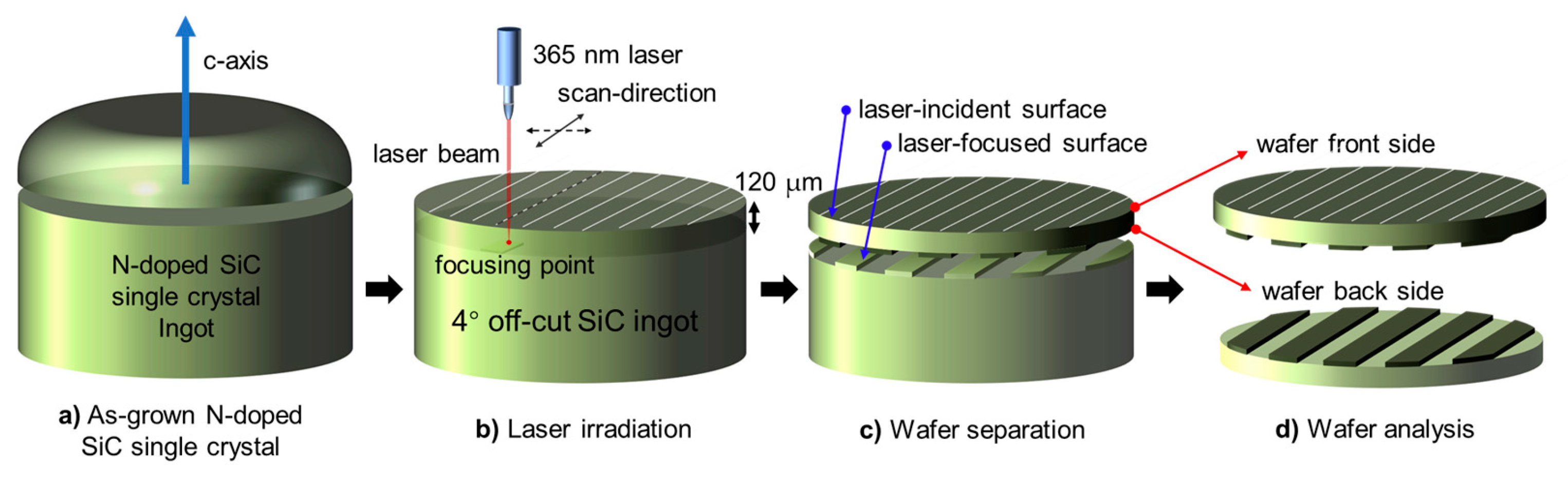
Figure 2.
SEM and EDS analyses of the laser-irradiated and laser-sliced SiC surfaces. (a) Low-magnification SEM image of the laser-irradiated surface showing periodic laser tracks with a spacing of ~203 μm. (b,c) High-magnification SEM images of regions 1 and 2 from (a), revealing the surface morphology prior to wafer separation. (d) Low-magnification SEM image of the laser-sliced surface with a spacing of ~205 μm, exhibiting fracture features produced by subsurface laser modification. (e,f) High-magnification SEM images of regions 3 and 4 from (d), showing the microstructure of the laser-sliced fracture plane. (g,h) EDS spectra from the laser-irradiated surface (g) and the laser-sliced surface (h). The inset electron images confirm that both surfaces contain only Si and C without detectable contamination.3.2. Roughness Evolution.
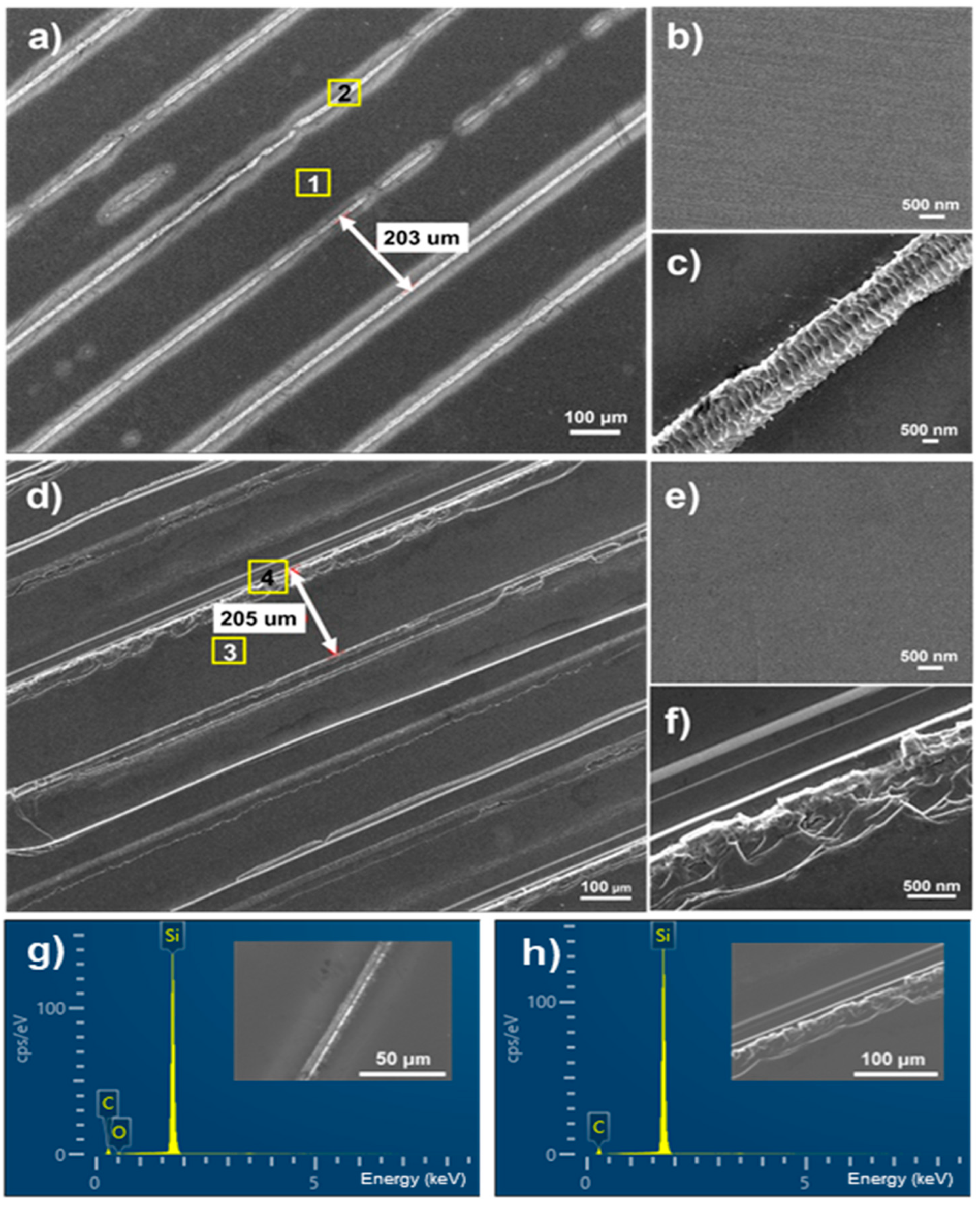
Figure 3.
AFM and SEM analyses of the laser-irradiated and laser-sliced SiC surfaces. SEM images of (a) the laser-irradiated surface and (b) the laser-sliced surface, with the probed AFM regions indicated. AFM 2D morphology and 3D topography were obtained from the laser-irradiated surface at (c,f) region 1 (20×20 μm², black square), (d,g) region 2 (20×20 μm², yellow square), and (e,h) a 1×1 μm² subregion within region 2. For the laser-sliced surface, AFM measurements were collected from (i,m) region 3 (20×20 μm², red square), (j,n) a 1×1 μm² subregion within region 3, (k,o) region 4 (20 × 20 μm², blue square), and (l,p) a 1×1 μm² subregion within region 4. Regions 1–4 correspond to the laser-irradiated area, smooth area, hill area, and valley area, respectively. Diagonal lines in the AFM images indicate the directions along which surface roughness profiles were extracted.
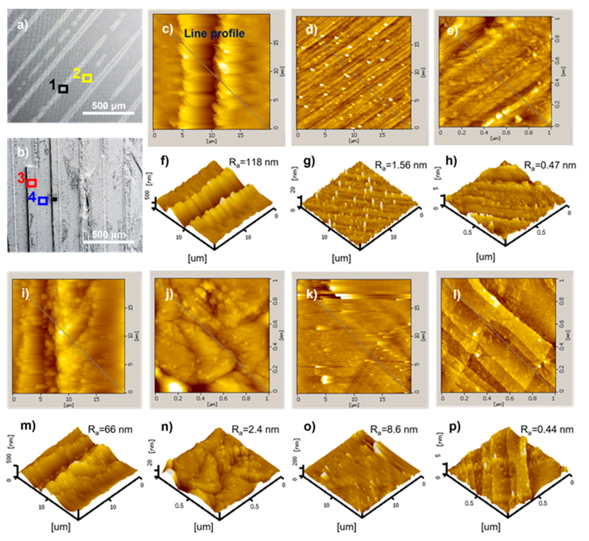
Figure 4.
Structural and Raman analyses of the 4H–SiC wafer and laser-irradiated surface. (a) XRD θ–2θ scan showing the (0004) and (0008) reflections of 4H–SiC, confirming c-axis–oriented single crystallinity. The inset shows the φ-scan of the (0004) reflection, indicating the absence of in-plane rotational domains. (b) Rocking curve (ω-scan) of the (0004) peak with a FWHM of 138 arcsec, demonstrating high crystalline quality and low mosaic spread. The schematic inset illustrates the 4° off-axis geometry toward the [11,12,13,14,15,16,17,18,19,20] direction. The (0004) pole figure inset (χ = 0° at the center) exhibits a single sharp intensity maximum corresponding to the c-axis orientation. (c) Raman spectra collected from two representative regions of the laser-irradiated surface, with the inset optical image showing the probed positions (regions 1 and 2). Characteristic 4H–SiC folded transverse optical (FTO), folded longitudinal optical (FLO), and folded longitudinal acoustic (FLA) modes are identified. (d) Enlarged Raman spectra in the 700–1200 cm⁻¹ range highlighting the dominant FTO (1/2) and FLO (0) modes for both regions. The FLO (0) peak was fitted using a coupled LO phonon–plasmon model, yielding an electron concentration of ~3.1×10¹⁸ cm⁻³.
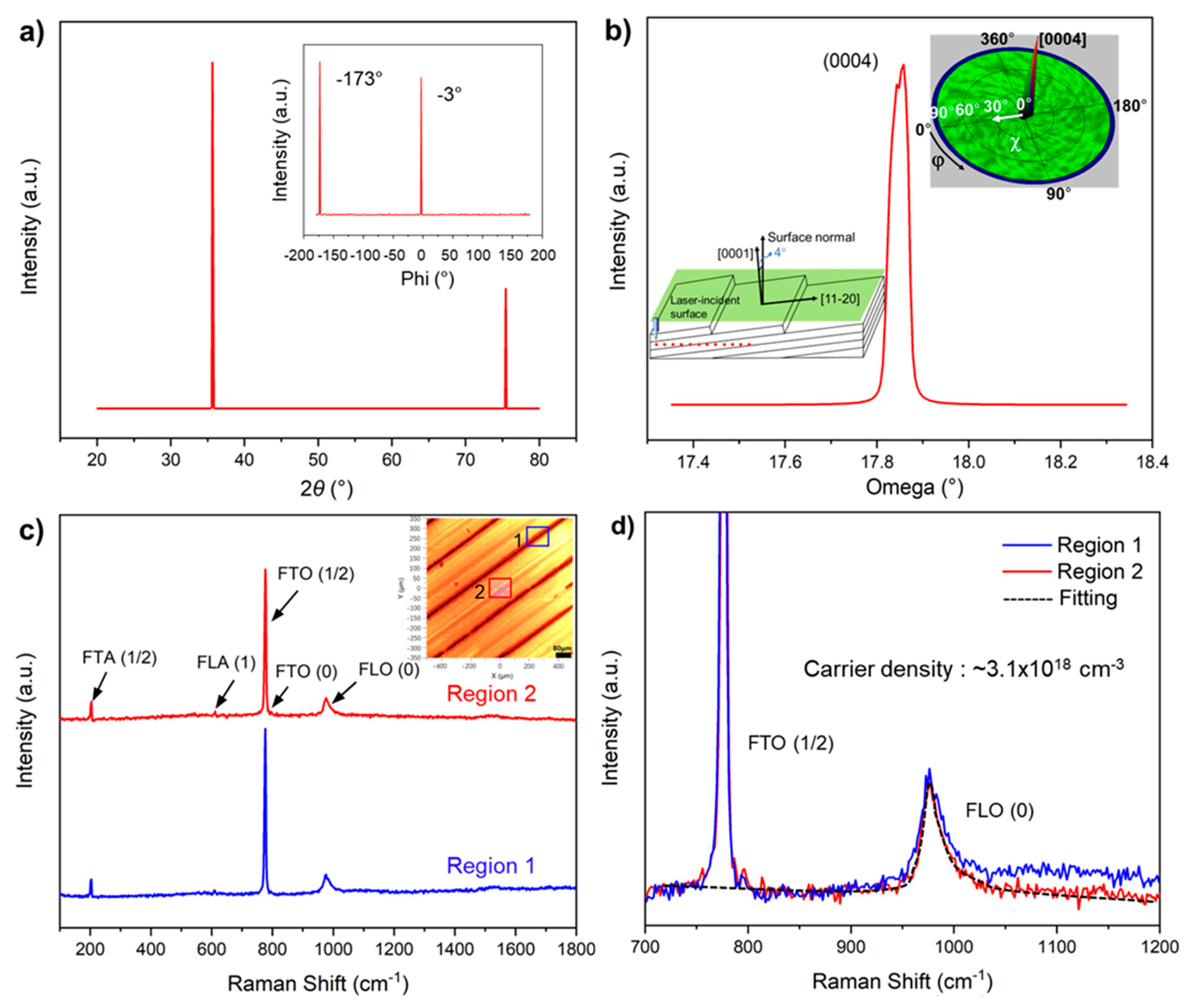
Figure 5.
TEM, SAED, HAADF-STEM, and EDS analyses of laser-processed SiC. (a) Cross-sectional TEM image of the smooth laser-irradiated surface near the SiC/Pt interface. (b,c) Cross-sectional TEM images of the laser-sliced region, corresponding to the hill area (b) and valley area (c). The insets in (a–c) present the SAED patterns obtained from each region, confirming the crystalline orientation and structural features. (d,e) HAADF-STEM images and corresponding EDS elemental maps (Pt, Si, C, N, O) for the laser-irradiated side (d) and the laser-sliced side (e), illustrating the elemental distribution across the SiC bulk, interface, and laser-modified areas.
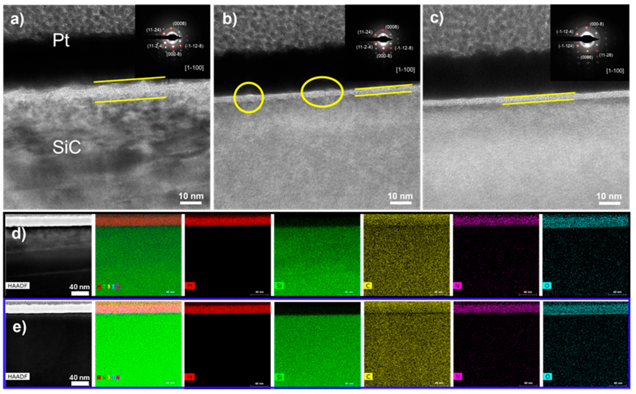
Figure 6.
Angle-resolved XPS spectra of laser-processed SiC surfaces. (a) ARXPS spectra of the laser-irradiated surface and (b) the laser-sliced surface, showing the C 1s, O 1s, N 1s, and Si 2p core-level regions measured at take-off angles ranging from 28° to 78°. All spectra were charge-corrected by referencing the adventitious C 1s (C–C/C–H) peak at 284.6 eV. The surface-normal direction was defined as 0°, with higher take-off angles corresponding to surface-parallel emission. During ARXPS acquisition, the X-ray incidence angle remained fixed, and photoelectrons were collected simultaneously along six emission directions via the hemispherical analyzer.
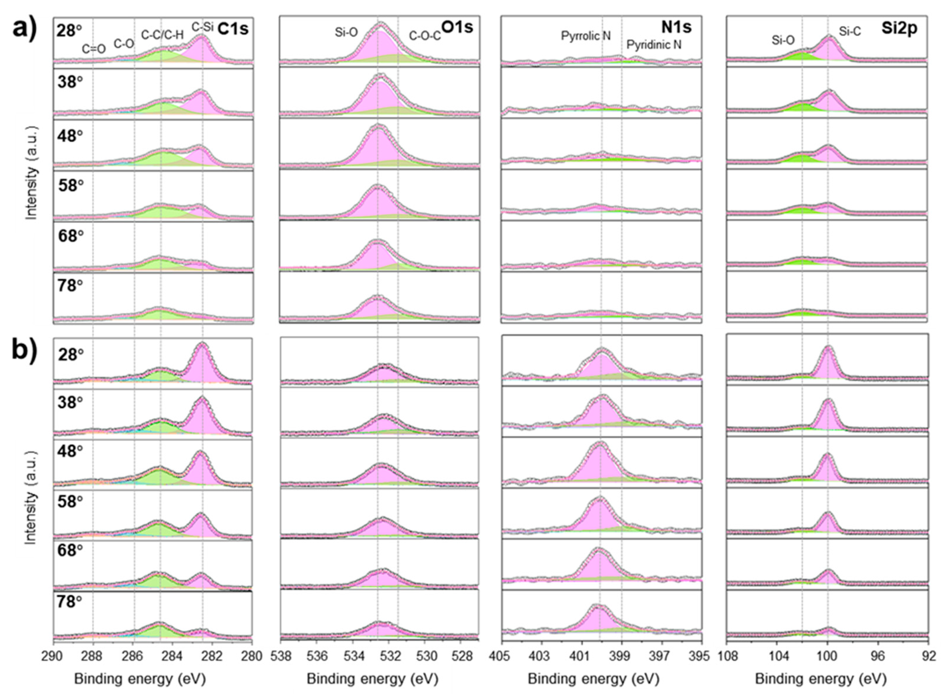
Figure 7.
Two-dimensional XPS chemical-state maps of laser-processed SiC surfaces. (a,b) Chemical-state mapping of the laser-irradiated surface (a) and the laser-sliced surface (b) obtained from deconvoluted C 1s, O 1s, N 1s, and Si 2p spectra. The mapped components include C–Si (~283.0 eV), C–C/C–H (~285.0 eV), C–O/C=O (~286–288 eV), Si–C (~100.5 eV), and Si–O (~103.5 eV). The laser-sliced surface additionally shows nitrogen-related signals assigned to pyridinic N (~398.4 eV) and pyrrolic N (~400.3 eV). The color contrast reflects the relative intensities of each bonding state, enabling comparison of the spatial chemical distribution between the two surfaces.
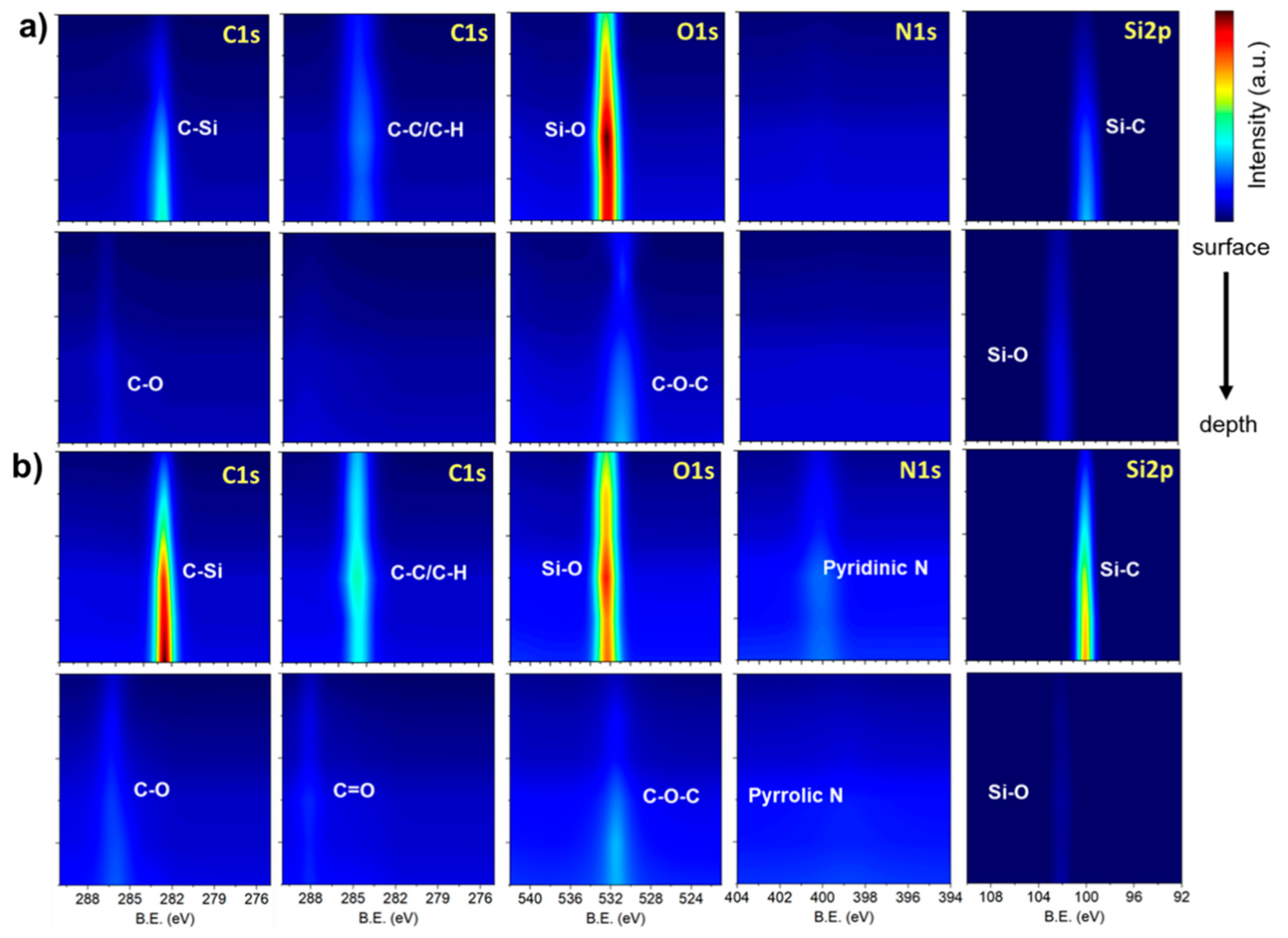
Figure 8.
SIMS images and depth profiles of laser-processed SiC surfaces. (a,b) O₂⁺-beam SIMS ¹²C⁺ and ³⁰Si⁺ ion images (2D and 3D) from the laser-irradiated surface (a) and the laser-sliced surface (b) over a 250 × 250 μm² area. (c,d) Cs⁺-beam SIMS depth profiles for the laser-irradiated (c) and laser-sliced (d) surfaces, showing N and O concentrations (left axis) and Si and C matrix ion intensities (right axis) as a function of sputter depth.
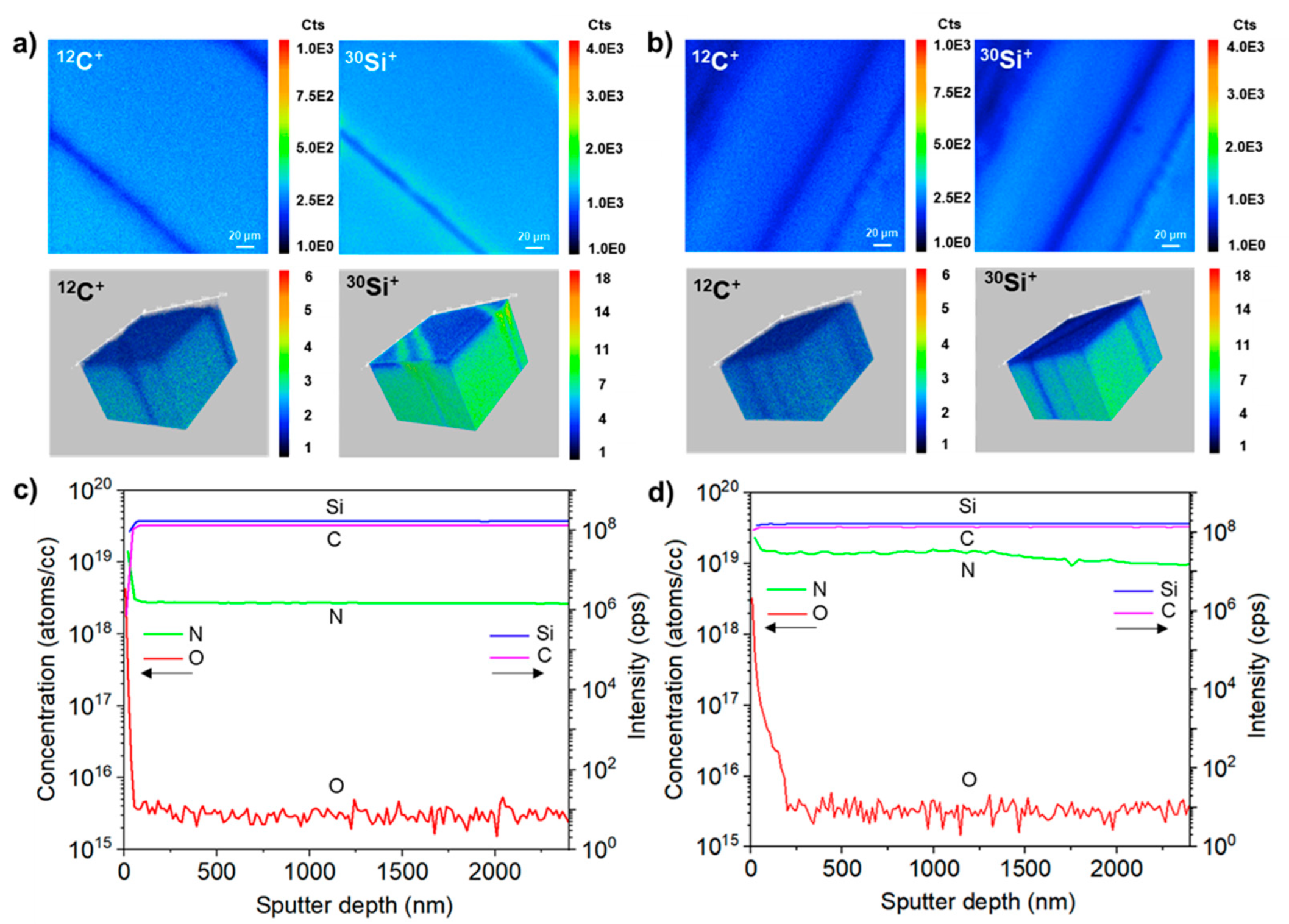
Figure 9.
Schematic illustration of the UV laser slicing process and the resulting separation surface morphology. A focused UV laser (λ=365 nm) is scanned across the SiC ingot to create a periodic subsurface modified layer that serves as the cleavage plane. The detached wafer exhibits a well-defined hill–valley structure that directly reflects the laser scanning pitch, with the hill region showing slightly higher roughness due to localized laser focusing. This laser-based slicing method provides key advantages, including near-zero kerf loss, clean and low-damage separation surfaces, high material utilization, and efficient production of ultra-thin SiC wafers.
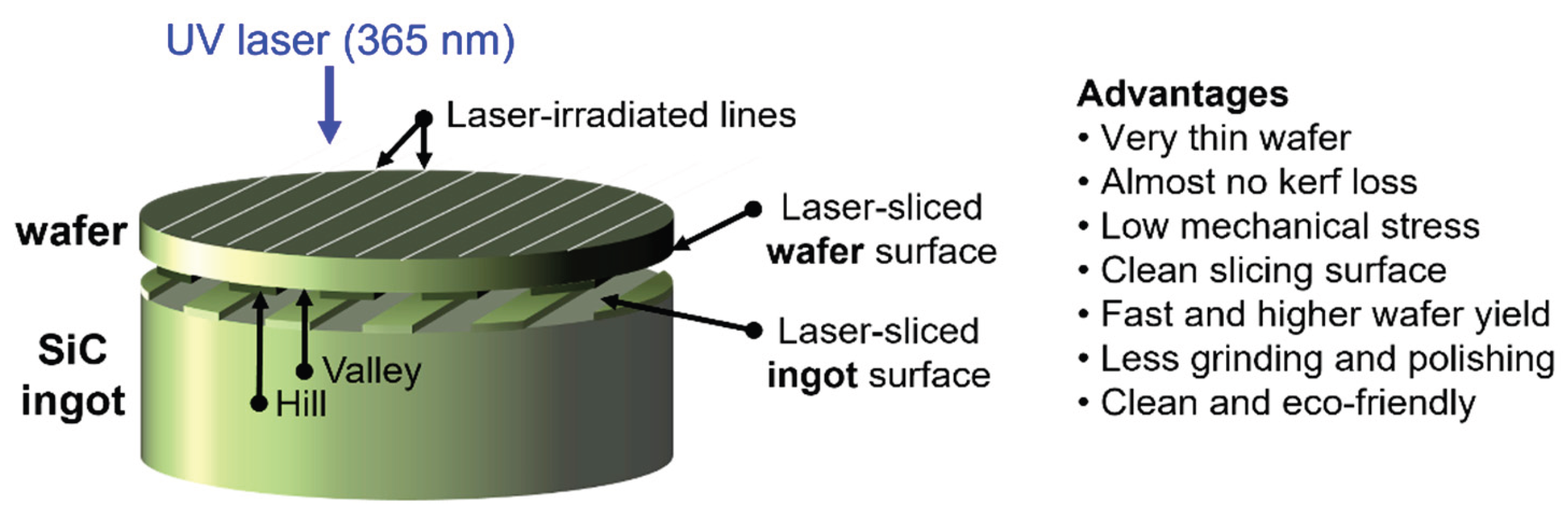
Disclaimer/Publisher’s Note: The statements, opinions and data contained in all publications are solely those of the individual author(s) and contributor(s) and not of MDPI and/or the editor(s). MDPI and/or the editor(s) disclaim responsibility for any injury to people or property resulting from any ideas, methods, instructions or products referred to in the content. |
© 2025 by the authors. Licensee MDPI, Basel, Switzerland. This article is an open access article distributed under the terms and conditions of the Creative Commons Attribution (CC BY) license (http://creativecommons.org/licenses/by/4.0/).
Copyright: This open access article is published under a Creative Commons CC BY 4.0 license, which permit the free download, distribution, and reuse, provided that the author and preprint are cited in any reuse.


