Submitted:
21 November 2025
Posted:
24 November 2025
You are already at the latest version
Abstract
This study examines the impact of incorporating a thin gold (Au) nanofilm as an interfacial buffer layer between the anode and the active layer in poly(3-hexylthiophene-2,5-diyl):[6,6]-phenyl-C₆₁-butyric acid methyl ester (P3HT:PCBM) organic solar cells. A nominal 6 nm Au layer was thermally evaporated onto indium tin oxide (ITO) substrates and subsequently annealed at 550 °C for 30 and 60 minutes before completing the device fabrication. The optical, morphological, and electrical consequences of introducing these annealed Au films were systematically evaluated. Optical measurements revealed a marked enhancement in light absorption: the unannealed Au/P3HT:PCBM film showed a 54% increase at 560 nm, rising to 79% after 60 minutes of annealing, attributed to localized surface plasmon resonance. In contrast, electrical characterization indicated a decline in overall photovoltaic performance, with all parameters decreasing except for a modest 2% increase in fill factor. Atomic force microscopy further revealed that the actual Au nanofilm thickness was approximately 16 nm—significantly higher than the nominal 6 nm—leading to increased roughness and aggregation. The excessive thickness and roughened morphology of the annealed Au film likely hindered charge transport and reduced exciton generation by scattering and reflecting incident light away from the active layer. These findings highlight the competing effects of Au nanofilms: while they enhance optical absorption, they simultaneously degrade electrical performance. This underscores the importance of carefully optimizing nanofilm thickness and morphology to achieve a balanced interplay between plasmonic enhancement and electronic transport in organic solar cells.
Keywords:
organic solar cells
; anodic layer
; Au thinfilm
; annealing
; localized surface plasmon resonance
; negative impact
1. Introduction
Organic solar cells (OSCs) have emerged as promising candidates to replace conventional inorganic solar cells due to their unique advantages, including low-temperature and low-cost solution processing, lightweight nature, mechanical flexibility, and portability [1,2,3]. Among the various materials used in OSCs, the polymer poly(3-hexylthiophene-2,5-diyl) (P3HT) and the fullerene derivative [6,6]-phenyl-C61-butyric acid methyl ester (PCBM) represent the most extensively investigated donor–acceptor pair in bulk heterojunction (BHJ) configurations. In this system, the interpenetrating nanoscale network formed by P3HT (electron donor) and PCBM (electron acceptor) facilitates efficient exciton dissociation and charge transport toward the electrodes, achieving single-junction efficiencies of up to 6% under standard illumination conditions (AM 1.5G, 100 mW·cm⁻2, 25°C) [4,5].
Significant research efforts have been devoted to enhancing the power conversion efficiency (PCE) of OSCs. Strategies include the design of novel donor polymers and non-fullerene acceptors [6,7], the development of tandem [8,9] and ternary architectures [10,11], which have together raised efficiencies to around 10% [5]. Despite these advancements, the PCE of OSCs remains below that of commercial inorganic solar cells. The relatively short exciton diffusion length in organic materials necessitates thin active layers to enable efficient charge separation, but this simultaneously limits light absorption [12,13,14,15].
To mitigate this trade-off between optical absorption and exciton dissociation, several enhancement techniques have been explored, including the integration of plasmonic nanostructures [16,17,18,19,20], quantum dots [21,22], and graphene-based materials [23,24]. Among these, noble metallic nanoparticles have shown notable potential for improving OSC performance through localized surface plasmon resonance (LSPR), which amplifies the local electromagnetic field and enhances light absorption by up to two orders of magnitude [25,26]. Our previous studies demonstrated that embedding gold nanorods in different layers of the OSC devices—such as the active layer [2], buffer layer [1], and cathodic layer [3] —can yield approximately 21% enhancement in PCE.
Although noble metal nanostructures, particularly Au nanoparticles and nanofilms, have been extensively investigated for enhancing light absorption in OSCs through LSPR, most studies have primarily focused on their positive influence on device performance. Numerous reports have demonstrated efficiency improvements when metallic nanostructures are incorporated within the active or buffer layers; however, the potential adverse or detrimental effects of these nanostructures—arising from variations in film thickness, morphology, or annealing conditions—remain largely unexplored.
Specifically, the interdependent effects of Au nanofilm thickness, nanoscale roughness, and annealing-driven morphological evolution have not been systematically examined in relation to charge transport and charge-collection dynamics in P3HT:PCBM-based OSCs. Moreover, prior studies have largely overlooked the possibility that incorporating Au interlayers may detrimentally affect device operation, whether through excessive optical reflection, uncontrolled light scattering, or the creation of interfacial trap states that hinder efficient carrier extraction. Consequently, a critical knowledge gap persists regarding how the structural transformations induced by annealing in ultrathin Au nanofilms govern both the optical field distribution and the electrical performance of P3HT:PCBM devices, particularly when the Au layer is positioned at the anode interface. Clarifying this interplay is essential for establishing the design criteria under which plasmonic metallic interlayers can genuinely enhance, rather than inadvertently compromise, organic solar cell efficiency.
In this study, we systematically investigate the effect of incorporating a thin Au nanofilm into the anodic layer of P3HT:PCBM-based OSCs. A nominal 6 nm Au film was thermally evaporated onto indium tin oxide (ITO)-coated glass substrates and subsequently annealed at 550 °C for 30 and 60 minutes prior to the deposition of the remaining layers. The optical, morphological, and electrical characteristics of the fabricated devices were comprehensively analyzed to elucidate the dual role of Au nanofilms in modulating light absorption and charge transport within the active layer. The increased thickness and roughness of the annealed Au film likely impeded charge transport and reduced exciton generation through light scattering and reflection. This underscores the need to optimize Au nanofilm morphology to balance optical benefits with electrical performance in organic solar cells.
2. Materials and Fabrication
2.1. Chemical Materials
All chemicals and materials were used as received without any further purification. The polymer P3HT with a high regioregularity of 98%, was obtained from Rieke Metals. The hole transport and buffer layer material, poly(3,4-ethylenedioxythiophene):poly(styrenesulfonate) (PEDOT:PSS) (CLEVIOS™ P VP AI 4083), was purchased from HC Starck. The fullerene derivative PCBM (>99.5%) and the solvent 1,2-dichlorobenzene (anhydrous, 99%) were supplied by Sigma-Aldrich. Gold (Au), aluminum (Al), and lithium fluoride (LiF) were obtained from Alfa Aesar.
Figure 1 illustrates the chemical structures of P3HT and PCBM, which together constitute the active layer of the fabricated organic solar cell devices.
2.2. Instrumentation
The surface structure was characterized using scanning electron microscopy (FEG-SEM Hitachi S-4700) with an accelerating voltage ~1-2KV. The morphology was also tested using the scanning mode of atomic force microscopy (AFM NanoInk's DPN 5000). A double-beam spectrophotometer (PerkinElmer LAMBDA 650) was used to measure the UV-vis spectra profiles. All tested samples were measured in the visible range of the spectra (~300-850). A solar simulator (Oriel Instruments) of a xenon lamp and AM 1.5G filter was used to characterize the organic solar cell devices under ambient conditions. A light meter (Bioscience LI-250) was used to calibrate the lamp's intensity to 100 mW/cm2. An electrometer (Keithley 2400) was used to measure the current-voltage output. A spin-coater (Laurell WS-650Mz-23NPPB) was used to obtain the active layer film (P3HT:PCBM). A thermal evaporator (Tecuum VCM 600 V1) was used to evaporate Ag, Li and Al. A hotplate, ultrasonic bath and plasma etcher were also used in the fabrication process of OSCs.
2. Experimental Procedures
The fabrication steps for the organic solar cell (OSC) devices are illustrated in Figure 2, following the procedures described in references [1,2,3]. ITO-coated glass substrates were first cut to the desired dimensions, patterned using a UV lamp, and thoroughly cleaned with a mild detergent solution. The substrates were then sequentially sonicated in acetone, isopropanol, and deionized water for 10 minutes each. After cleaning, they were dried under a nitrogen stream and baked at 150 °C for 20 minutes to remove residual moisture. Subsequently, the substrates underwent oxygen plasma treatment to enhance surface wettability and improve the adhesion of the following layers.
Next, the aqueous solution of the buffer layer material, PEDOT:PSS, was spin-coated onto the treated ITO substrates and baked at 120 °C for 30 minutes under ambient conditions to form a uniform thinfilm. For the deposition of the active layer, the substrates were transferred to a nitrogen-filled glove box, where a P3HT:PCBM blend solution was spin-coated at 1000 rpm to form the bulk heterojunction (BHJ) layer.
Finally, the cathode was deposited by thermal evaporation under a high vacuum (<10⁻⁶ torr), consisting of a bilayer structure of lithium fluoride (LiF, ~6 nm) and aluminum (Al, ~90 nm), using a shadow mask. Each substrate contained eight identical device cells with an active area of 0.16 cm2. The complete device architecture and layer configurations are shown in Figure 3.
For the devices incorporating the Au nanofilm, a gold layer with an approximate thickness of 6 nm was thermally evaporated onto the pre-cleaned ITO-coated glass substrates. The coated substrates were then placed on a hotplate and annealed at 550 °C for 30 and 60 minutes to induce nanostructural formation and improve film uniformity. Following the annealing process, the remaining device layers were sequentially deposited according to the fabrication procedure described above. Figure 4 displays the SEM image of the pristine device layers for comparison.
3. Measurements and Discussion
3.1. The Optical Measurement of Au Nanofilms
Figure 5(a) presents the UV–Vis absorbance spectra of 6 nm-thick Au films before and after annealing at 550 °C for 30 and 60 minutes. The pristine Au nanofilm exhibits a distinct plasmonic absorption peak at 605 nm within the visible range. Upon annealing, the peak experiences a blue shift to 576 nm, accompanied by a reduction in absorption intensity of approximately 3% and 11% for 30- and 60-minute annealing durations, respectively. These plasmonic absorption peaks arise from LSPR—the collective oscillation of free electrons at the interface between two media of differing dielectric constants—which results in strong light absorption and scattering within the visible spectrum [27,28]. Annealing the nanofilm promotes the transformation of the continuous Au layer into irregular or semi-spherical nanoparticles that sustain LSPR, as confirmed by the SEM and AFM micrographs shown in Figure 6 and Figure 7. The morphology, size, and surface density of these nanoparticles depend strongly on the annealing time and temperature [29,30,31].
The observed blue shift in the plasmonic peak after annealing can be attributed to the quantum confinement effect, indicating a reduction in the average nanoparticle size [32,33]. Moreover, the appearance of shoulder features in the absorption spectra of the annealed films (Figure 5a) suggests that the nanoparticles are not perfectly spherical, leading to the presence of a secondary resonance mode [1]. When the annealing duration was further increased to 120 minutes, this secondary plasmonic peak became more pronounced, as shown in the supplementary figures.
Importantly, the absorption band of the Au nanofilms overlaps significantly with that of the P3HT:PCBM active layer (400–650 nm), as illustrated in Figure 5(b). This spectral overlap indicates the potential for plasmonic enhancement of light absorption within the active layer of the organic solar cells.
3.2. The Structural Measurement of Au Nanofilms
Figure 6 presents the SEM micrographs of the Au nanofilms annealed at 550 °C for 30 and 60 minutes, while Figure 7 shows the corresponding AFM images. Both SEM and AFM analyses reveal that annealing significantly alters the microstructure and surface morphology of the Au nanofilms, leading to the formation of discrete Au nanostructures.
As revealed from the AFM, prolonging the annealing duration from 30 to 60 minutes results in a pronounced increase in surface roughness, with the root-mean-square (RMS) roughness rising from 2.35 nm to 4.98 nm. This increase in roughness is attributed to the coalescence and growth of Au nanoparticles during thermal treatment, which induces morphological reconstruction and nanoparticle aggregation. The annealing time, therefore, serves as a key parameter in tuning the nanoparticle size and surface morphology, which in turn influences the crystallinity, optical absorption characteristics, and plasmonic behavior of the nanostructured Au films [34,35].
3.3. The Optical Properties of Au/P3HT:PCBM Films
Figure 8 illustrates the UV–Vis absorption spectra of the pristine P3HT:PCBM film and the Au/P3HT:PCBM composite films, both before and after annealing at 550 °C for 30 and 60 minutes. The pristine P3HT:PCBM film exhibits a characteristic absorption band between 420 and 620 nm, with a primary absorption peak centered at 520 nm and two distinct shoulders at approximately 560 and 600 nm. These features correspond to the π–π* transitions and vibronic structures of the P3HT backbone, indicative of its degree of molecular ordering [4,36]. Upon incorporating the Au nanofilm (without annealing), the absorption spectrum shows a noticeable red shift and a significant enhancement in intensity, particularly at the 560 nm shoulder, which increases by approximately 54% and becomes the dominant peak. This enhancement arises from the plasmonic near-field effect of the Au nanostructures, which amplifies the local electromagnetic field within the active layer [27,37]. Further annealing of the Au/P3HT:PCBM films at 550 °C for 30 and 60 minutes results in an additional increase in absorption intensity, reaching up to 79% enhancement relative to the pristine P3HT:PCBM film. The improvement in optical absorption can be attributed to the optimized formation of Au nanoparticles during annealing, which promotes stronger LSPR coupling and enhanced light–matter interaction within the active layer.
3.4. The Effect of the Annealed Au Nanofilms on OSC Parameters
Since annealing the Au nanofilm for 60 minutes resulted in the highest enhancement of P3HT:PCBM film absorptivity, this condition was selected for integration into practical OSC devices. designed to investigate the influence of the Au nanofilm and PEDOT:PSS buffer layer on charge extraction and hole-collection efficiency at the anode interface, four sets of devices were fabricated simultaneously, for comparative analysis. These configurations, as previously illustrated in Figure 3, are: (a) Without buffer layer: ITO/P3HT:PCBM/LiF–Al (b) With buffer layer: ITO/PEDOT:PSS/P3HT:PCBM/LiF–Al, (c) With Au and buffer layer: ITO/Au/PEDOT:PSS/P3HT:PCBM/LiF–Al (d) With Au but without buffer layer: ITO/Au/P3HT:PCBM/LiF–Al.
Figure 9 presents the current density–voltage (J–V) characteristics of the devices under illumination (a) and in the dark (b), both before and after deposition of the Au film. The corresponding photovoltaic (PV) parameters—including open-circuit voltage (VOC), short-circuit current density (JSC), fill factor (FF), and power conversion efficiency (PCE)—are summarized in Table 1. The series resistance (RS) was extracted from the dark J–V curves at approximately 0.86 V.
The dark J–V characteristics of all fabricated devices (Figure 9b) demonstrate well-defined rectifying behavior, confirming good diode performance. Under illumination, the photovoltaic parameters summarized in Table 1 reveal that the best device performance was achieved for the configuration incorporating the PEDOT:PSS anodic buffer layer. This device exhibited a PCE of 1.6%, primarily attributed to a JSC of 3.74 mA·cm⁻2.
Introducing the Au nanofilm beneath the buffer layer led to a modest improvement in the FF, increasing from 67.67% to 69.09%, which can be ascribed to a reduction in the RS and improved charge transport at the anode interface. However, both the VOC and JSC slightly decreased, resulting in an overall 26% reduction in PCE compared to the reference device (device with PEDOT:PSS). In contrast, devices fabricated with the Au nanofilm but without the PEDOT:PSS buffer layer exhibited significantly degraded performance, characterized by reductions in all key photovoltaic parameters— VOC, JSC, FF, and PCE—indicating that the direct contact between the Au nanostructured layer and the active layer negatively affects charge extraction and device efficiency.
Figure 10 illustrates the work functions of all materials utilized in the fabricated devices. The work function of the PEDOT:PSS buffer layer is well aligned with both the work function of the ITO electrode and the highest occupied molecular orbital (HOMO) level of the P3HT polymer. This favorable energy-level alignment explains the superior performance of the device incorporating the buffer layer compared to the one without it. The effective matching of work functions facilitates efficient hole transport from the active layer to the anode, thereby enhancing charge collection and improving the overall device performance [38,39].
Although introducing the Au nanolayer between the ITO and the PEDOT:PSS buffer layer resulted in a 24% increase in JSC and a 2% improvement in FF, the overall PCE decreased by 26%, primarily due to a 5% reduction in VOC. This decline in device efficiency was somewhat unexpected, considering that the annealed Au nanofilm significantly enhanced the optical absorption of the P3HT:PCBM active layer. The observed reduction in VOC may be attributed to interfacial energy-level mismatches or increased recombination losses at the Au/buffer interface, which counteracted the optical gains provided by the plasmonic enhancement.
As reported in previous studies [29,30,31,40], the electrical and morphological properties of gold films are strongly influenced by several factors, including annealing conditions, crystallinity, surface contamination, and roughness. Thermal annealing of Au films promotes grain growth and induces nanostructural irregularities, which consequently increase the surface roughness. Such morphological changes can adversely affect charge transport and collection by the anodic electrode in multiple ways. Increased surface roughness can hinder efficient charge extraction by reducing the number of free charge carriers reaching the electrode, delaying charge dissipation [41], and introducing surface-state energy defects [42] that serve as recombination centres. Moreover, excessive roughness at the electrode interface can distort the internal electric field distribution within the device, thereby altering the motion and balance of charge carriers [43,44]. These combined effects could plausibly explain the observed 5% reduction in the open-circuit voltage VOC in our Au-integrated devices, despite the improvement in optical absorption.
To verify the actual thickness of the Au nanofilm, AFM measurements were performed, as shown in Figure 11. The measured film thickness was approximately 16 nm, which is notably higher than the intended 6 nm. This deviation may partially account for the observed reduction in device performance upon incorporating the Au nanofilm. The formation of a relatively dense Au nanostructured layer at the anode interface can hinder efficient hole collection and negatively impact light harvesting. The increased film thickness and surface coverage may obstruct light penetration into the active region, either by scattering or reflecting incident photons away from the P3HT:PCBM layer [45,46]. Consequently, fewer excitons are generated, leading to a reduced population of free charge carriers reaching the electrodes. Collectively, these effects contribute to the observed decrease in VOC and overall device efficiency.
4. Conclusion
In this study, we investigated the effect of incorporating an Au nanofilm as an interfacial layer between the ITO anode and the P3HT:PCBM active layer in OSCs. Thin Au films (6 nm) were thermally evaporated onto ITO-coated glass substrates and subsequently annealed at 550 °C for 30 and 60 minutes prior to the deposition of the remaining device layers. The influence of the annealed Au films on the device performance was systematically examined through optical, morphological, and electrical analyses.
The Au nanofilms demonstrated excellent transparency and electrical conductivity, with a distinct optical absorption feature at 605 nm attributed to the LSPR of Au nanostructures. Upon annealing, this peak blue-shifted to 576 nm, accompanied by a reduction in intensity of 3% and 11% for 30- and 60-minute annealing durations, respectively. SEM and AFM analyses revealed that annealing promoted nanoparticle growth, increased surface roughness, and enhanced crystallinity, leading to structural evolution in the Au nanofilms.
Photovoltaic measurements of devices with and without Au and/or buffer layers showed that the device incorporating the conventional anodic buffer layer exhibited the highest performance, achieving a PCE of 1.6%. Although the Au nanofilm possesses a work function that aligns well with both the ITO electrode and the HOMO level of P3HT, replacing the buffer layer with the Au nanofilm only improved the FF by 2%, while the overall PCE decreased. This decline in performance was unexpected, given the 79% enhancement in optical absorption of the P3HT:PCBM film upon introducing the annealed Au nanofilm.
The observed reduction in device efficiency can be attributed to morphological and interfacial effects induced by annealing. Grain growth and surface irregularities increase surface roughness, leading to delayed charge dissipation, formation of surface-state defects, and enhanced carrier recombination. AFM analysis further revealed that the actual thickness of the deposited Au nanofilm was approximately 16 nm—substantially higher than the intended value—resulting in excessive optical scattering and reflection at the anode interface. These effects limit the amount of light reaching the active layer, reducing exciton generation and charge collection efficiency.
Overall, while the incorporation of Au nanofilms modifies the optical and structural properties beneficially, excessive film thickness and surface roughness negatively influence charge transport and extraction. Future optimization of Au nanofilm thickness and annealing conditions may yield a balanced enhancement in both optical absorption and device performance.
Supplementary Materials
The following supporting information can be downloaded at the website of this paper posted on Preprints.org.
Funding
This research received no external funding.
Data Availability Statement
The original contributions presented in this study are included in the article/supplementary material. Further inquiries can be directed to the corresponding author.
Acknowledgments
The author acknowledges with thanks the University of Jeddah for its research facilities.
Conflicts of Interest
The author reports no conflicts of interest. The author alone is responsible for the content and writing of this article.
References
- Alaa, Y. Mahmoud, Jianming Zhang, Dongling Ma, Ricardo Izquierdo, Vo-Van Truong. Optically-enhanced performance of polymer solar cells with low concentration of gold nanorods in the anodic buffer layer. Organic Electronics 2012, 13, 3102–3107. [Google Scholar]
- Alaa, Y. Mahmoud, Jianming Zhang, Dongling Ma, Ricardo Izquierdo, Vo-Van Truong. Thickness dependent enhanced efficiency of polymer solar cells with gold nanorods embedded in the photoactive layer. Solar Energy Materials & Solar Cells 2013, 116, 1–8. [Google Scholar]
- Alaa, Y. Mahmoud, Ricardo Izquierdo, Vo-Van Truong. Gold Nanorods Incorporated Cathode for Better Performance of Polymer Solar Cells, Journal of Nanomaterials 2014, 2014, 1–7. [Google Scholar]
- Christoph, J. Brabec, Srinivas Gowrisanker, Jonathan J. M. Halls, Darin Laird, Shijun Jia, Shawn P. Williams. Polymer–Fullerene Bulk-Heterojunction Solar Cells. Advanced Materials 22 September 2010, 8, 3839–3856. [Google Scholar] [CrossRef]
- Juanjuan Wang, Shengli Jia, Yang Cao, Wenhao Wang, Peng Yu. Design Principles for Nanoparticle Plasmon-Enhanced Organic Solar Cells. Nanoscale Research Letters 2018, 12, 1–6. [Google Scholar]
- Mahnoor Qaisar, Saba Zahid, Rasheed Ahmad Khera, Yaser A. El-Badry, Muhammad Umar Saeed, Rana Farhat Mehmood, Javed Iqbal. Molecular Modeling of Pentacyclic Aromatic Bislactam-Based Small Donor Molecules by Altering Auxiliary End-Capped Acceptors to Elevate the Photovoltaic Attributes of Organic Solar Cells. ACS Omega 2022, 7, 1–14. [Google Scholar] [CrossRef]
- Lulu Sun, Kenjiro Fukuda, Takao Someya. Recent progress in solution-processed flexible organic photovoltaics. npj Flexible Electronics, 2022; 6. [CrossRef]
- Zhenrong Jia, Shucheng Qin, Lei Meng, Qing Ma, Indunil Angunawela, Jinyuan Zhang, Xiaojun Li, Yakun He, Wenbin Lai, Ning Li, Harald Ade, Christoph J. Brabec, Yongfang Li. High performance tandem organic solar cells via a strongly infrared-absorbing narrow bandgap acceptor. Nature Communications volume, 2021; 12, 1–10.
- Jianqiu Wang, Jiayao Li, Yafei Wang, Junzhen Ren, Pengqing Bi, Huixue Li, Jiangbo Dai, Shaoqing Zhang, Jianhui Hou. Tandem Organic Solar Cells with 21.5% Efficiency. Advanced Materials 2025, 37, 1–13. [Google Scholar] [CrossRef]
- Marcella Günther, Negar Kazerouni, Dominic Blätte, Jose Dario Perea, Barry C. Thompson, Tayebeh Ameri. Models and mechanisms of ternary organic solar cells. Natur Reviews Materials 2023, 8, 456–471. [Google Scholar] [CrossRef]
- Ruijie Ma, Cenqi Yan, Jiangsheng Yu, Tao Liu, Heng Liu, Yuhao Li, Jian Chen, Zhenghui Luo, Bo Tang, Xinhui Lu, Gang Li, He Yan. High-Efficiency Ternary Organic Solar Cells with a Good Figure-of-Merit Enabled by Two Low-Cost Donor Polymers. ACS Energy Letters 2022, 7, 2547–2556. [Google Scholar] [CrossRef]
- Mohamed Shaban, Mohamed Benghanem, Abdullah Almohammedi and Mohamed Rabia. Optimization of the Active Layer P3HT:PCBM for Organic Solar Cell. Coatings 2021, 11, 1–15. [Google Scholar] [CrossRef]
- Nidhi Sharma, Saral K. Gupta, Chandra Mohan Singh Negi. Influence of active layer thickness on photovoltaic performance of PTB7:PC70BM bulk heterojunction solar cell. Superlattices and Microstructures, 2019; 135, 106278. [CrossRef]
- Yue Zang, Qing XinJufeng and ZhaoJun Lin. Effect of Active Layer Thickness on the Performance of Polymer Solar Cells Based on a Highly Efficient Donor Material of PTB7-Th. The Journal of Physical Chemistry C 2018, 122, 16532–16539. [Google Scholar] [CrossRef]
- Markus, C. Scharber. On the Effi ciency Limit of Conjugated Polymer:Fullerene-Based Bulk Heterojunction Solar Cells. Advanced Materials, 2001; 28, 1994–2001. [Google Scholar] [CrossRef]
- ine Benaya, Mohammed Madani Taouti, Khalid Bougnina, Bahri Deghfel, Abdelhalim Zoukel. Gold nanoparticles in P3HT: PCBM active layer: A simulation of new organic solar cell designs. Solid-State Electronics Volume 2025, 2025, 1–11. [Google Scholar] [CrossRef]
- H. P. Wang, S. Pigeon, R. Izquierdo, R. Martel. Electrical bistability by self-assembled gold nanoparticles in organic diodes. Applied Physic Letters 2006, 89, 1–3. [Google Scholar]
- C. R. Singh, T. Honold, T. P. Gujar, M. Retsch, A. Fery, M. Karg, M. Thelakkat. The role of colloidal plasmonic nanostructures in organic solar cells. Physical Chemistry Chemical Physics 2016, 18, 23255–23163. [Google Scholar]
- Iddo Diukman, Lior Tzabari, Nikolai Berkovitch, Nir Tessler, Meir Orenstein. Controlling absorption enhancement in organic photovoltaic cells by patterning Au nano disks within the active layer. Optics Express 2011, 19, 1–8. [Google Scholar]
- Pankaj Kumar Das, Anuj Dhawan. Plasmonic enhancement of photovoltaic characteristics of organic solar cells by employing parabola nanostructures at the back of the solar cell. RSC Advances 2023, 13, 26780–26792. [Google Scholar] [CrossRef]
- Se-Woong Baek, Sunhong Jun, Byeongsu Kim, Andrew H. Proppe, Olivier Ouellette, Oleksandr Voznyy, Changjo Kim, Junho Kim, Grant Walters, Jung Hoon Song, Sohee Jeong, Hye Ryung Byun, Mun Seok Jeong, Sjoerd Hoogland, F. Pelayo García de Arquer, Shana O.. Efficient hybrid colloidal quantum dot/organic solar cells mediated by near-infrared sensitizing small molecules. Nature Energy volume 2019, 4, 969–976. [Google Scholar] [CrossRef]
- Ming Chen, Jiuxing Wang, Feifei Yin, Zhonglin Du, Laurence A. Belfiorec, Jianguo Tang. Strategically integrating quantum dots into organic and perovskite solar cells. Journal of Materials Chemistry A 2021, 9, 4505–4527. [Google Scholar] [CrossRef]
- Jinhong Du, Dingdong Zhang, Xiao Wang, Hui Jin, Weimin Zhang, Bo Tong, Yu Liu, Paul L. Burn, Hui-Ming Cheng, Wencai Ren. Extremely efficient flexible organic solar cells with a graphene transparent anode: Dependence on number of layers and doping of graphene. Carbon 2021, 171, 350–358. [Google Scholar] [CrossRef]
- Jaehoon Kim, RAshis K. Sarker, Yeseul Park, Jeonghun Kwak, Hyung-Jun Song, Changhee Lee. Study on graphene oxide as a hole extraction layer for stable organic solar cells. RSC Advances 2021, 11, 1–8. [Google Scholar] [CrossRef]
- Jyh-Lih Wu, Fang-Chung Chen, Yu-Sheng Hsiao, Fan-Ching Chien, Peilin Chen, Chun-Hong Kuo, Michael H. Huang, Chain-Shu Hsu. Surface Plasmonic Effects of Metallic Nanoparticles on the Performance of Polymer Bulk Heterojunction Solar Cells. CS Nano 2011, 5, 959–967. [Google Scholar]
- M. Pelton, J. Aizpurua, G. Bryant. Metal-Nanoparticle Plasmonics. Laser & Photonics Reviews 2008, 2, 136–159. [Google Scholar]
- Jacob Waitkus, Yu Chang, Li Liu, Srinivasu Valagerahally Puttaswamy, Taerin Chung, Adrian M. Molina Vargas, Stephen J. Dollery, Mitchell R. O’Connell, Haogang Cai, Gregory J. Tobin, Nikhil Bhalla, and Ke Du. Gold Nanoparticle Enabled Localized Surface Plasmon Resonance on Unique Gold Nanomushroom Structures for On-Chip CRISPR-Cas13a Sensing. Advanced Materials 2023, 10, 1–9. [Google Scholar]
- Mohammad, A. Alebrahim, Ahmad A. Ahmad, A.B. Migdadi, Qais M. Al-Bataineh. Localize surface plasmon resonance of gold nanoparticles and their effect on the polyethylene oxide nanocomposite films. Physica B: Condensed Matter 2024, 679, 1–10. [Google Scholar]
- Maktoof, A.S. , Mohammed, G.H. & Abbas, H.H.. Effect of annealing process on structural and optical properties of Au-doped thin films (NiO:WO3) fabricated by PLD technique. Journal of Optics 2025, 54, 2204–2215. [Google Scholar] [CrossRef]
- Mantas Sriubas, Vytautas Kavaliūnas, Kristina Bočkutė, Paulius Palevičius, Marius Kaminskas, Žilvinas Rinkevičius, Minvydas Ragulskis, Giedrius Laukaitis. Formation of Au nanostructures on the surfaces of annealed TiO2 thin films. Surfaces and Interfaces, 2021; 25, 101239. [CrossRef]
- N. Milićević, M. Novaković, J. Potočnik, M. Milović, L. Rakočević, N. Abazović, D. Pjević. Influencing surface phenomena by Au diffusion in buffered TiO2-Au thin films: Effects of deposition and annealing processing. Surfaces and Interfaces, 2022; 30. [CrossRef]
- Peng S, McMahon JM, Schatz GC, Gray SK, Sun Y. . Reversing the size-dependence of surface plasmon resonances. PNAS 2010, 107, 14530–14534. [Google Scholar] [CrossRef] [PubMed]
- Kerry, J. Lee, Tao Huang, Prakash D. Nallathamby, and Xiao-Hong Nancy Xu. Wavelength Dependent Specific Plasmon Resonance Coupling of Single Silver Nanoparticles with EGFP. Nanoscale, 2015; 7, 17623–17630. [Google Scholar] [CrossRef]
- Puran Pandey, Sundar Kunwar, Mao Sui, Ming-Yu Li, Quanzhen Zhang, Jihoon Lee. Effect of Annealing Temperature on Morphological and Optical Transition of Silver Nanoparticles on c-Plane Sapphire. Journal of Nanoscience and Nanotechnology, 2018; 18, 3466–3477. [CrossRef]
- Jaroenporn Chokboribal, Watcharapon Vanidshow, Weeraya Yuwasonth, Chanunthorn Chananonnawathorn, Uraiwan Waiwijit, Wantanee Hincheeranun, Kittidhaj Dhanasiwawong, Mati Horprathum, Tanattha Rattana, Supphadate Sujinnapram, Wuttichai Phae-ngam. Annealed plasmonic Ag nanoparticle films for surface enhanced fluorescence substrate. Materials Today: Proceedings, 2021, 47, 3492–3495. [Google Scholar] [CrossRef]
- Mosè Casalegno,*Antonino Famulari, and Stefano Valdo Meille. Modeling of Poly(3-hexylthiophene) and Its Oligomer’s Structure and Thermal Behavior with Different Force Fields: Insights into the Phase Transitions of Semiconducting Polymers. Macromolecules 2022, 55, 2398–2412. [Google Scholar] [CrossRef]
- Harry, A. Atwater, Albert Polman. Plasmonics for Improved Photovoltaic Devices. Nature Materials 2010, 9, 205–213. [Google Scholar]
- Xi Fan, Nathan E. Stott, Jixi Zeng, Yunfei Li, Jianyong Ouyang, Liang Chu and Weijie Song. PEDOT:PSS materials for optoelectronics, thermoelectrics, and exible and stretchable electronics. Journal of Materials Chemistry A 2023, 11, 1–31. [Google Scholar]
- Qi Bin Ke, Jia-Ren Wu, Chia-Chen Lin, Sheng Hsiung Chang. Understanding the PEDOT:PSS, PTAA and P3CT-X Hole-Transport-Layer-Based Inverted Perovskite Solar Cells. Polymers, 2022. [CrossRef]
- Leonid Chernyak, Andrei Osinsky, Alfons Schulte. Minority carrier transport in GaN and related materials. Solid-State Electronics 2001, 45, 1687–1702. [Google Scholar] [CrossRef]
- Yan Jiang, Shan Zhang, Wanheng Lu, Chi Kit Ao, Kang Wen Lim, Kaiyang Zeng, Siowling Soh. Nanocavities stabilize charge: Surface topology is a general strategy for controlling charge dissipation. Materials Today Physics 2023, 35, 1–11. [Google Scholar] [CrossRef]
- Gulou Shen, Haoguang Yang, Yongke Hu, Xiaojie Zhang, Feng Zhou, Huaju Li and Kun Hong. Impact of Surface Roughness on Partition and Selectivity of Ionic Liquids Mixture in Porous Electrode. Nanomaterials 2023, 13, 1–13. [Google Scholar] [CrossRef]
- Sanjoy Kumar Nandi, Xinjun Liu, Dinesh Kumar Venkatachalam, Robert Glen Elliman. Effect of Electrode Roughness on Electroforming in HfO2 and Defect-Induced Moderation of Electric-Field Enhancement. Physical Review Applied, 2015; 4, 1–11. [CrossRef]
- M. Z. Kabir; Mahboob Liaquat. Effects of non-uniform electric field on the charge collection efficiency in radiation detectors: Deviation from Hecht formula. Journal of Applied Physics 2015, 138, 1–9. [Google Scholar] [CrossRef]
- F. C. Chen, J.L. Wu, C.L. Lee, Y. Hong, C.H. Kuo, M.H. Huang,. Plasmonic- enhanced polymer photovoltaic devices incorporating solution- processable metal nanoparticles, Applied Physics Letters 2009, 95, 1–3. [Google Scholar] [CrossRef]
- Carlos Israel Medel-Ruiz, Roger Chiu, Jesús Ricardo Sevilla-Escoboza and Francisco Javier Casillas-Rodríguez. Nanoscale Surface Roughness Effects on Photoluminescence and Resonant Raman Scattering of Cadmium Telluride. Applied Sciences 2024, 14, 1–12. [Google Scholar] [CrossRef]
Figure 1.
The chemical structures for the polymer P3HT and the fullerene PCBM.
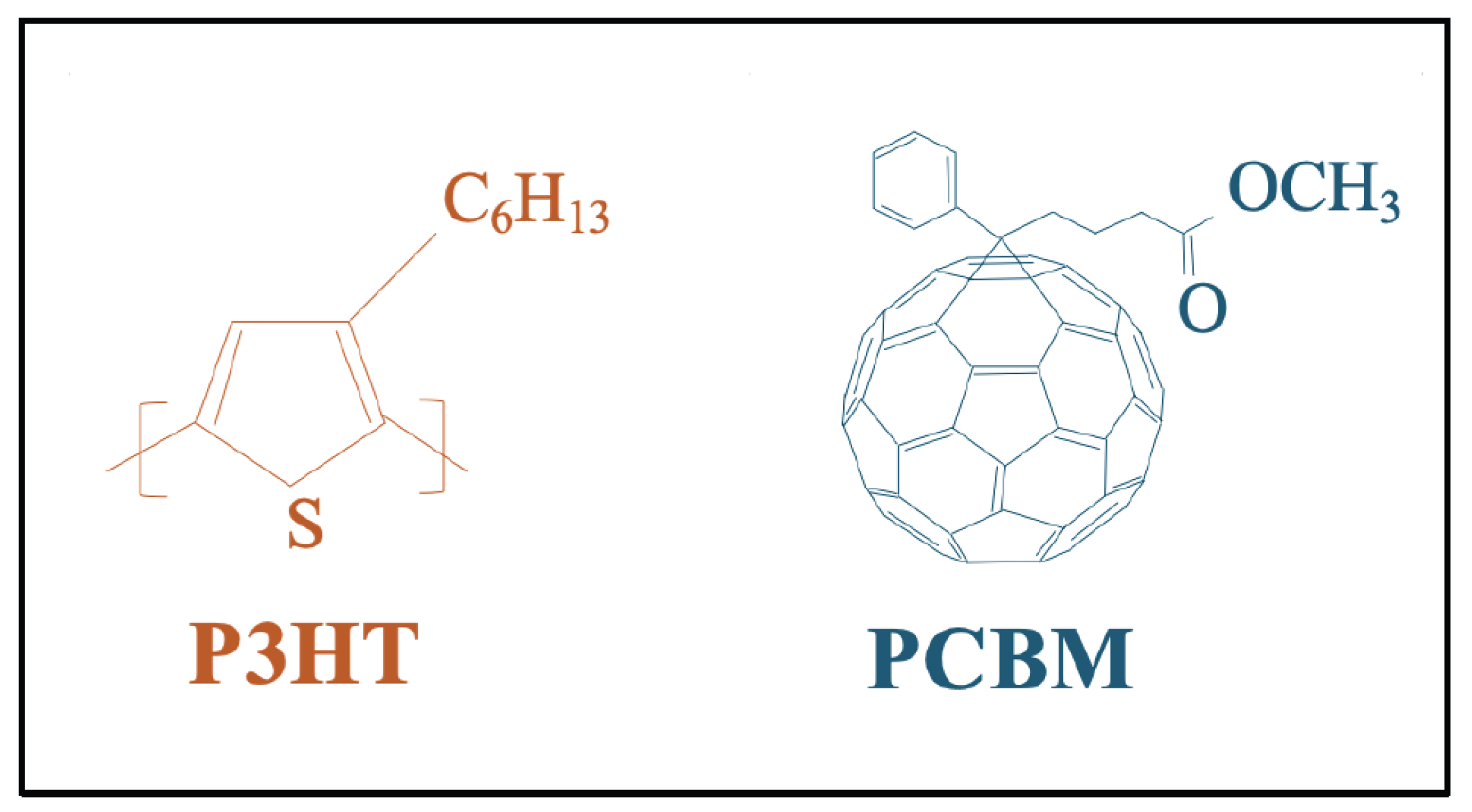
Figure 2.
The fabrication steps of the OSC device.
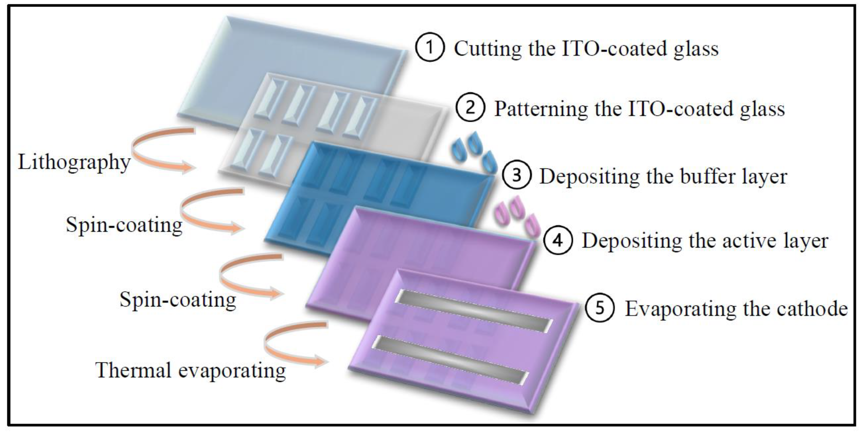
Figure 3.
The final configurations of the experimental devices (a) without both Au-nanofilm and buffer layer (b) without Au-nanofilms and with buffer layer, (c) with both Au-nanofilm and buffer, (d) with Au nanofilms without buffer layer.
Figure 3.
The final configurations of the experimental devices (a) without both Au-nanofilm and buffer layer (b) without Au-nanofilms and with buffer layer, (c) with both Au-nanofilm and buffer, (d) with Au nanofilms without buffer layer.
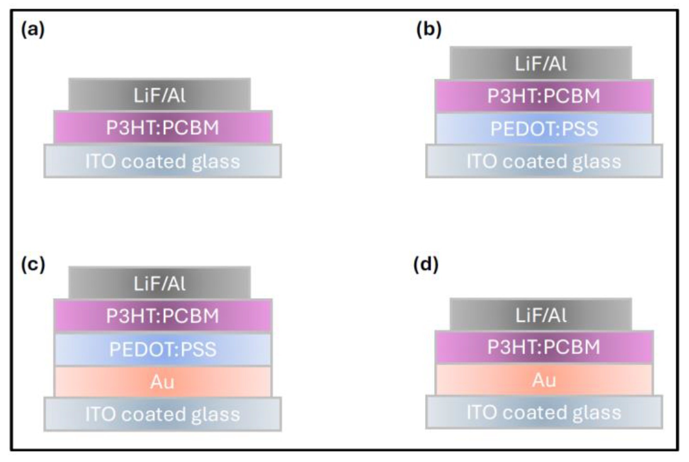
Figure 4.
The SEM micrograph for the pristine OSC device layers showing their thicknesses.
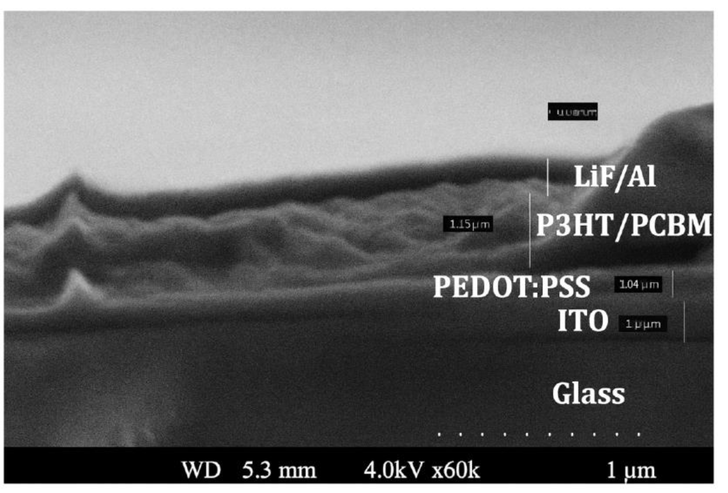
Figure 5.
The absorbance profile for the (a) evaporated Au and (b) spin-coated P3HT:PCBM nanofilms.
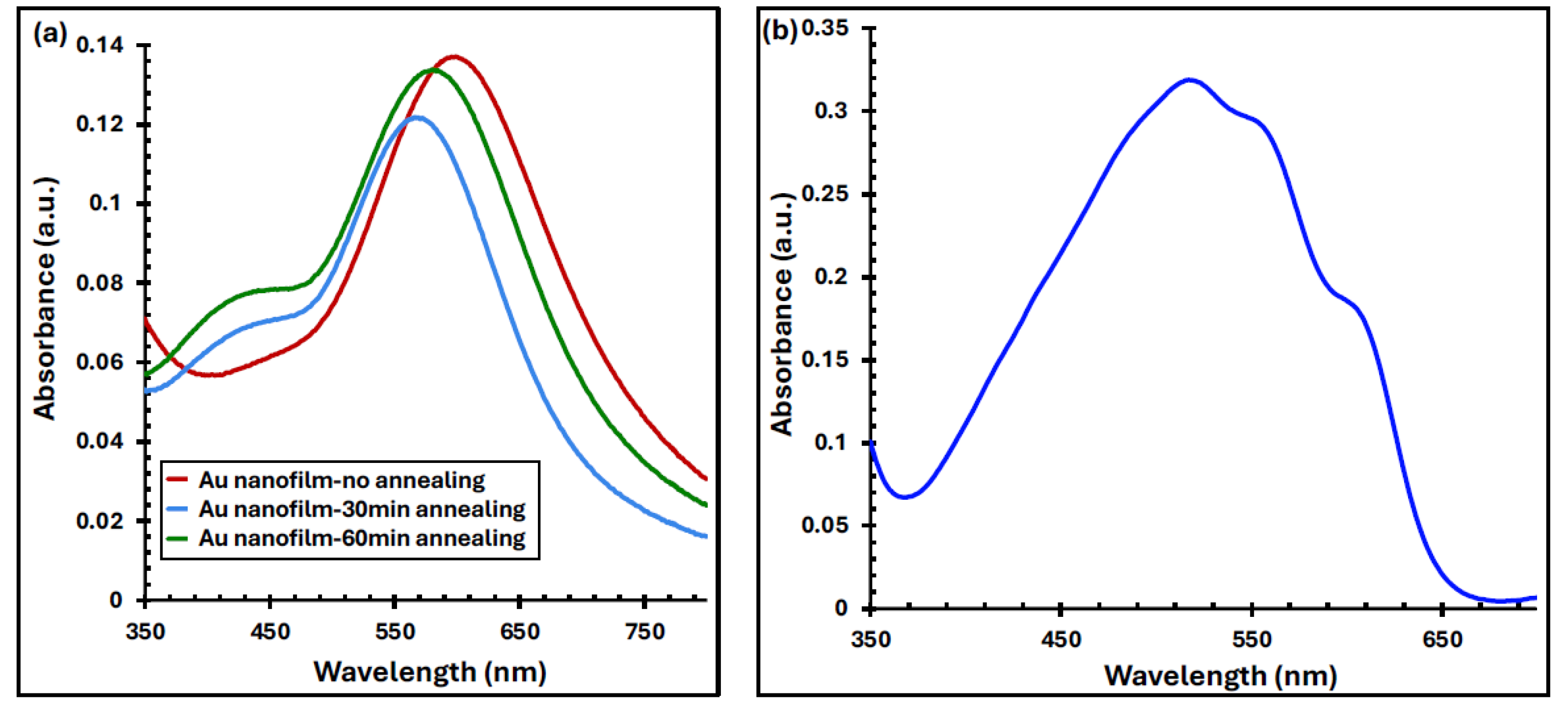
Figure 6.
The SEM images for Au nanofilm deposited on ITO-coated glass after annealing at 550°C for (a) 30 and (b) 60 minutes.
Figure 6.
The SEM images for Au nanofilm deposited on ITO-coated glass after annealing at 550°C for (a) 30 and (b) 60 minutes.
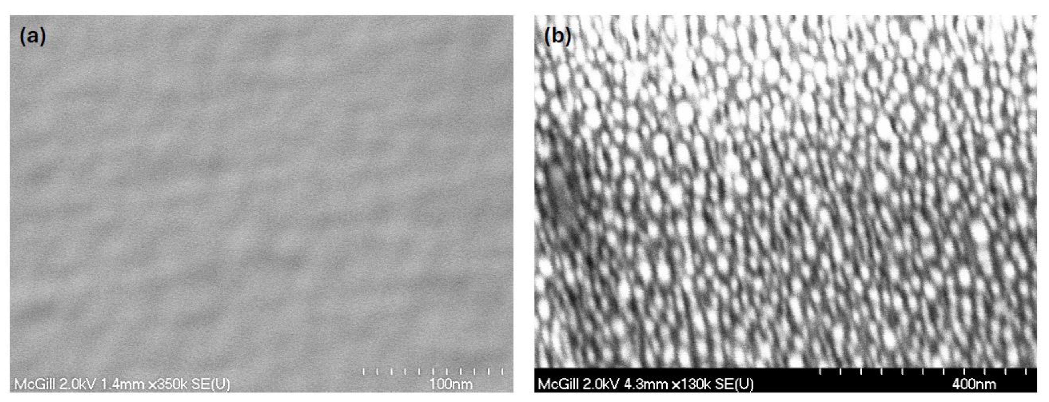
Figure 7.
The AFM (a) height and (b) phase images for the Au nanofilms annealed at 550°C for 30 and 60 minutes.
Figure 7.
The AFM (a) height and (b) phase images for the Au nanofilms annealed at 550°C for 30 and 60 minutes.

Figure 8.
The absorbance profile for Au/P3HT:PCBM film before and after annealing at 550 oC for 30 and 60 min, along with the absorbance of the pristine P3HT:PCBM.
Figure 8.
The absorbance profile for Au/P3HT:PCBM film before and after annealing at 550 oC for 30 and 60 min, along with the absorbance of the pristine P3HT:PCBM.
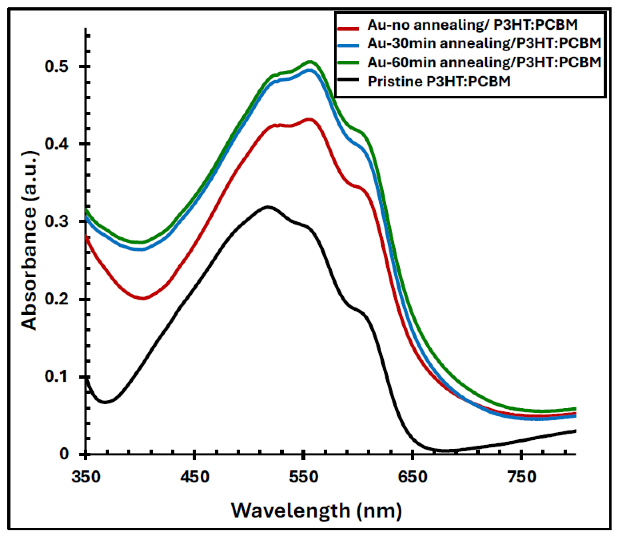
Figure 9.
The IV characteristics for OSC devices with and without Au film, along with devices without Au or buffer films (a) under light and (b) in the dark.
Figure 9.
The IV characteristics for OSC devices with and without Au film, along with devices without Au or buffer films (a) under light and (b) in the dark.
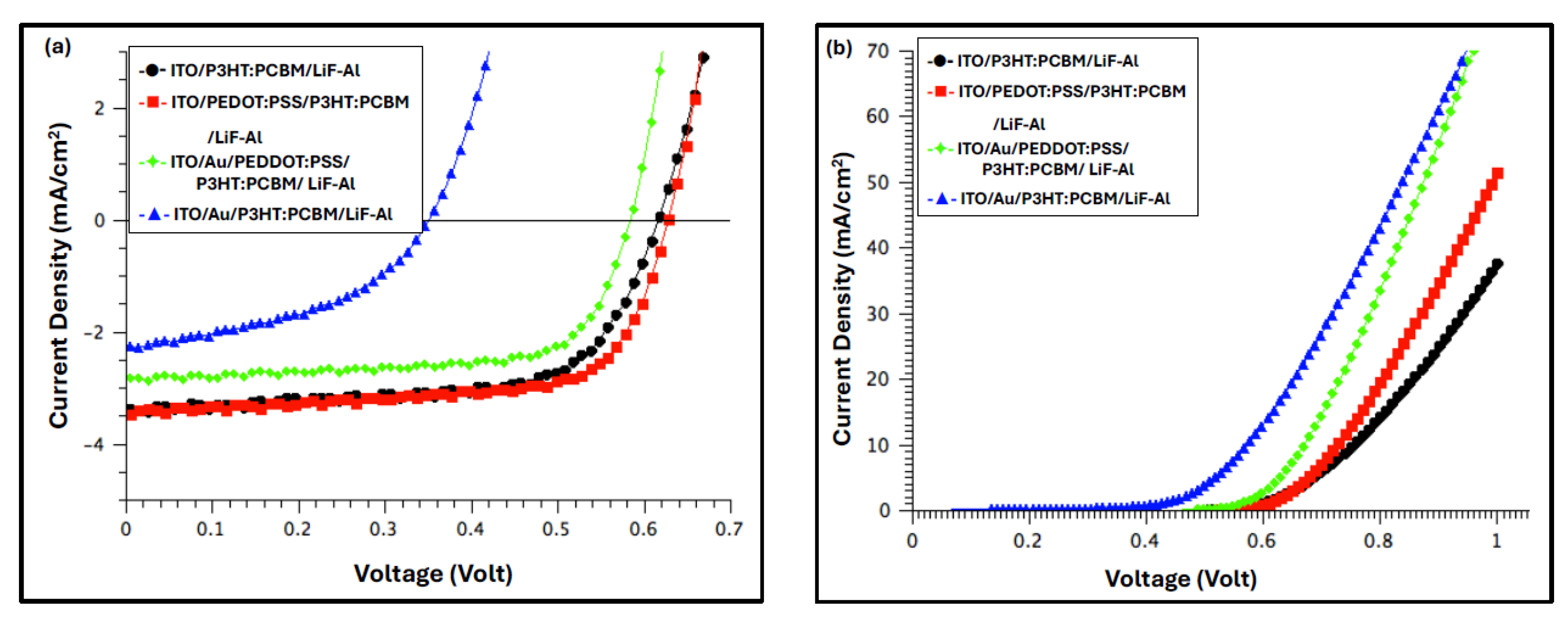
Figure 10.
Schematic illustration of the energy band alignment of the materials used in the fabricated devices. The work function of the PEDOT:PSS buffer layer effectively facilitates hole extraction and transport toward the anode. A good alignment is observed between the work function of Au, the HOMO level of the P3HT polymer, and the ITO anode work function, which supports efficient charge transfer at the interface. The energy level values are adapted from reference [1].
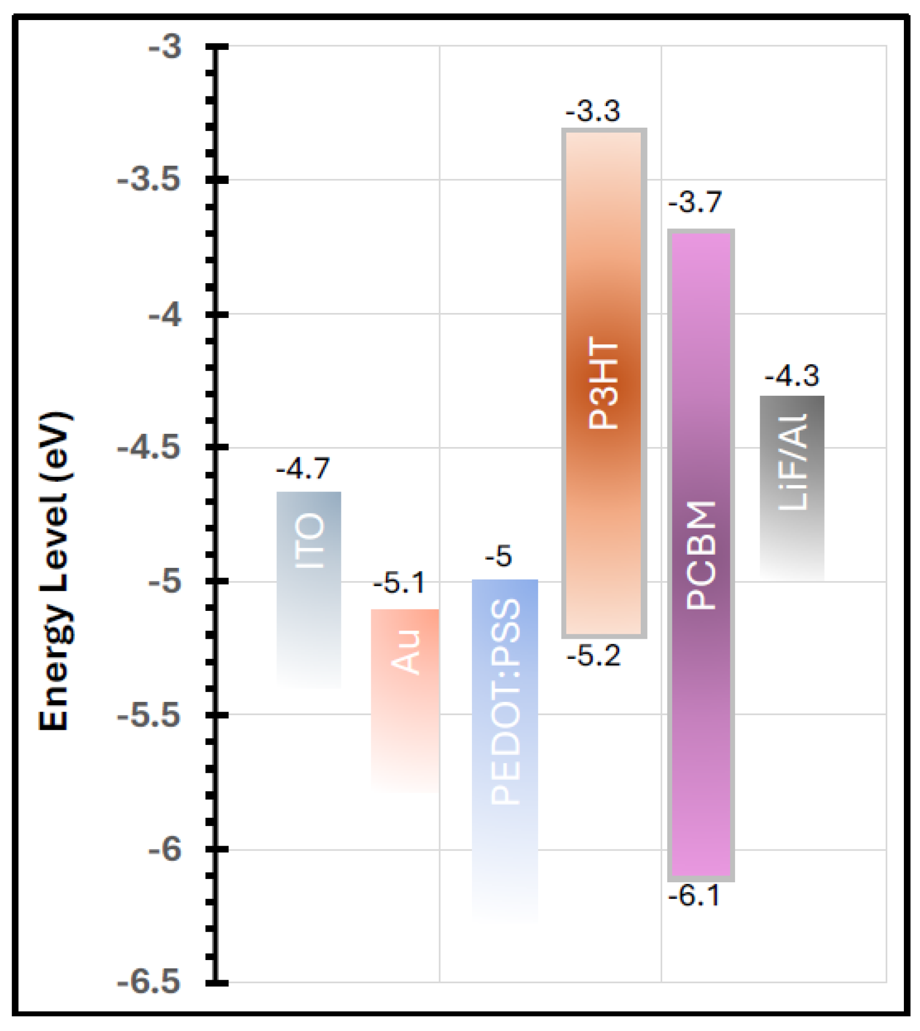
Figure 11.
(a) AFM topographic image of the thermally evaporated Au nanofilm, and (b) corresponding height profile showing an average film thickness of approximately 16 nm.
Figure 11.
(a) AFM topographic image of the thermally evaporated Au nanofilm, and (b) corresponding height profile showing an average film thickness of approximately 16 nm.
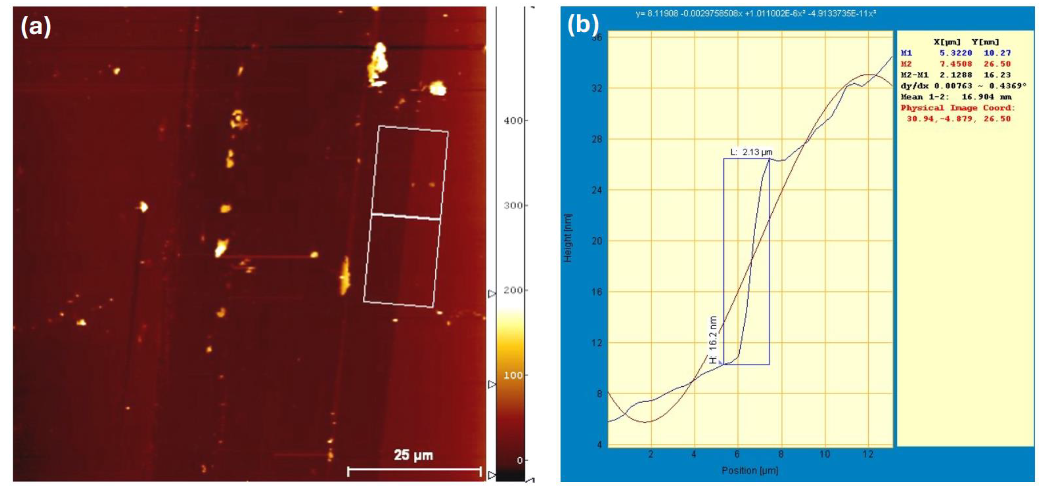

Table 1.
The OSCs’ PV parameters with and without Au nanofilm, along with devices without Au or buffer films.
Table 1.
The OSCs’ PV parameters with and without Au nanofilm, along with devices without Au or buffer films.
| Device configuration | VOC (V) | JSC (mA/cm2) | FF % | RS (mΩ) | PCE% | Δ % PCE |
|---|---|---|---|---|---|---|
| ITO/P3HT:PCBM/LiF-Al | 0.62 | -3.37 | 65.59 | 0.053 | 1.4 | -12% |
| ITO/PEDOT:PSS/ P3HT:PCBM/LiF-Al | 0.62 | -3.74 | 67.67 | 0.038 | 1.6 | - |
| ITO/Au/PEDOT:PSS/ P3HT:PCBM/LiF-Al | 0.59 | -2.84 | 69.09 | 0.025 | 1.2 | -26 % |
| ITO/Au/ P3HT:PCBM/Li-Al | 0.35 | -2.27 | 45.55 | 0.031 | 0.4 | - 77 % |
Disclaimer/Publisher’s Note: The statements, opinions and data contained in all publications are solely those of the individual author(s) and contributor(s) and not of MDPI and/or the editor(s). MDPI and/or the editor(s) disclaim responsibility for any injury to people or property resulting from any ideas, methods, instructions or products referred to in the content. |
© 2025 by the authors. Licensee MDPI, Basel, Switzerland. This article is an open access article distributed under the terms and conditions of the Creative Commons Attribution (CC BY) license (http://creativecommons.org/licenses/by/4.0/).
Copyright: This open access article is published under a Creative Commons CC BY 4.0 license, which permit the free download, distribution, and reuse, provided that the author and preprint are cited in any reuse.


