Submitted:
01 December 2025
Posted:
02 December 2025
You are already at the latest version
Abstract
Nanoimprint lithography (NIL) master fidelity is governed by coupled variations beginning with resist spin-coating, proceeding through electron-beam exposure, and culminating in anisotropic etch transfer. We present an integrated, physics-based simulation chain. First, it includes a spin-coating thickness model that combines Emslie–Meyerhofer scaling with a Bornside edge correction. The simulated wafer-scale map at 4000 rpm exhibits the canonical center-rise and edge-bead profile with a 0.190–0.206 μm thickness range, while the locally selected 600 nm × 600 nm tile shows <0.1 nm variation, confirming an effectively uniform region for downstream analysis. Second, it couples an e-beam lithography (EBL) module in which column electrostatics and trajectory-derived spot size feed a hybrid Gaussian–Lorentzian proximity kernel; under typical operating conditions ( ≈ 2–5 nm), the model yields low CD bias (ΔCD = 2.38/2.73 nm), controlled LER (2.18/4.90 nm), and stable NMSE (1.02/1.05) for isolated versus dense patterns. Finally, the exposure result is passed to a level-set reactive ion etching (RIE) model with angular anisotropy and aspect-ratio-dependent etching (ARDE), which reproduces density-dependent CD shrinkage trends (4.42% versus 7.03%) consistent with transport-limited profiles in narrow features. Collectively, the simulation chain accounts for stage-to-stage propagation—from spin-coating thickness variation and EBL proximity to ARDE-driven etch behavior—while reporting OPC-aligned metrics such as NMSE, ΔCD, and LER. In practice, mask process correction (MPC) is necessary rather than optional: the simulator provides the predictive model, metrology supplies updates, and constrained optimization sets dose, focus, and etch set-points under CD/LER requirements.
Keywords:
nanoimprint lithography (NIL)
; spin-coating thickness model
; E-beam lithography (EBL)
; reactive ion etching (RIE)
; mask process correction (MPC)
1. Introduction
1.1. Background and Motivation
Nanoimprint lithography (NIL) has attracted extensive interest as a low-cost and high-resolution patterning technique with the ability to replicate near-10-nm features over a large area [1,2,3]. The ongoing miniaturization of semiconductor devices has commonly been framed in the context of Moore’s law. While occasionally it is proclaimed that “Moore’s law is dead,” these proclamations are only partly true. While geometric scaling of feature sizes is nearing its physical limits, the enhancement of functional density and performance per unit area continues to be possible by employing novel lithographic techniques. In this context, NIL represents another dimension of progress, enabling performance scaling that is not solely dependent on shrinking the diffraction-limited resolution of conventional optical lithography. Recent industrial assessments further indicate that NIL maturation is accelerating, particularly as its applicability expands into semiconductor, LED, and photovoltaic manufacturing, where cost-efficient, high-resolution pattern replication is increasingly required. These developments underscore that NIL is advancing not only as a laboratory-scale patterning method but also as a technology transitioning toward broader industrial deployment, supported by improvements in materials, tooling, and replication workflows [4,5].
NIL is commonly acknowledged as one of the next-generation lithography (NGL) family members, and it plays a significant role in both microelectronics and other nanomanufacturing applications. As an NGL candidate, NIL offers a compelling balance of cost efficiency and resolution, which makes it an interesting complement or alternative to other advanced lithographic technologies [4,6].
The NIL process can be generally categorized into three stages: (i) master template fabrication, (ii) replica template production, and (iii) final wafer imprinting [7]. Among these stages, the fidelity of the master template is paramount, as it dictates the precision of both replica templates and wafer-level patterns. Recent advances in master-template electron-beam lithography have demonstrated hp10-nm and sub-10-nm patterning through resist–process co-optimization and SADP-based pattern multiplication, underscoring the continued importance of high-resolution template fabrication for NIL template performance [8]. Any imperfection in the master template is unavoidably passed on to the subsequent processes, rendering its fabrication as one of the most technically challenging tasks in the development of NIL [9,10,11,12]. Specifically, the surface roughness of the master template needs to be regulated at the low-nanometer level (approximately 2–3 nm root mean square (RMS)) to prevent demolding issues or defect formation during the NIL process [13,14].
In contrast to traditional photomasks, NIL master templates need to reconcile nanoscale resolution with resilience to multiple uses. Even slight variations in resist thickness or etch profile can result in cumulative distortions after being transferred to wafers [15,16]. Consequently, computational methods that anticipate systematic fabrication errors are becoming ever more necessary to aid process optimization and optical proximity correction (OPC) [17]. In particular, OPC not only serves to correct for process-induced distortions in the final patterns but also offers a pathway to optimize residual layer thickness and to reduce non-uniform resist distribution near shot-edge regions. These corrections are particularly critical for NIL, where residual layers and local resist filling behavior significantly impact the fidelity of the imprinted structures [18]. Recent studies on confinement-induced polymer flow resistance further show that nanoscale film thickness can significantly modulate flow mobility and apparent viscosity during cavity filling, reinforcing the need for physics-aware modeling of resist transport in NIL master-template fabrication [19]. Beyond these pattern-transfer considerations, maintaining template fidelity also requires accurate monitoring of alignment errors and subtle defect formation across multi-step imprinting. Advances in optical metrology—from Mie-resonator–base[15,16d overlay sensing to FDTD-driven inspection-stack optimization—have substantially improved sensitivity to overlay shifts and line-cut defects, thereby strengthening NIL process control and complementing OPC in ensuring consistent template quality [20,21].
In the OPC perspective, the master template is not a direct replica of the design layout but an pre-distorted pattern that compensates for process-induced distortions [15,16]. By introducing shape adjustments such as edge biasing, OPC ensures that, after resist development and etching, the final wafer structures produced more closely resemble the target design. Although the technique has been widely studied in optical lithography, its systematic integration into NIL template fabrication remains relatively underexplored [17].
A number of process variability sources complicate master template fabrication. First, resist spin-coating typically yields non-uniform thickness distributions, which modify local exposure response during EBL [3]. Second, the EBL process suffers from the proximity effect, wherein electron forward scattering, backscattering, and secondary electrons cause unwanted dose accumulation and pattern blur [4,7,22]. Third, RIE introduces anisotropy and microloading effects that distort sidewall angles and create etch depth non-uniformities [3,7]. Together, these error sources degrade dimensional control and pose critical challenges to NIL master template reliability.
To overcome these difficulties, this research constructs an integrated physics-based simulation framework that connects three multiphysical models: resist spin-coating, EBL exposure and development, and anisotropic RIE transfer. Through the coupling of these steps, the simulation captures the evolution of upstream variations—such as resist thickness non-uniformity—to downstream processes. While no experimental dataset is utilized here, the results are compared to known literature trends to verify their feasibility [23,24].
The proposed approach is part of the broader objective of integrating OPC optimization into predictive simulation frameworks. The integration is expected to minimize expensive fabrication iterations, offer early feedback during mask layout design, and eventually enhance wafer-level fidelity in NIL fabrication [4] [25].
1.2. Three Models Simulation and Parameter Setting
The fabrication of high-quality and durable master templates in NIL requires a judicious balance of material selection and process parameter optimization. Substrate and resist selection are of paramount importance, as they directly dominate dimensional stability, etch durability, and the reproducibility of nanoscale features. Silicon (Si) substrates have traditionally been the industry standard due to their exceptional mechanical strength, thermal stability, and sub-nanometer surface flatness that routinely achieves an RMS roughness of less than 1 nm. These qualities afford a robust platform for high-resolution patterning, in addition to guaranteeing compatibility with following EBL and RIE steps [26,27,28,29,30]. These qualities are also essential for master templates, where surface integrity and long-term durability are requisites for large-scale NIL replication [31,32].
On this foundation, the resist material determines the achievable resolution and the fidelity of pattern transfer. In this work, we used the positive-tone resist CSAR 62 AR-P 6200.09. This chemically semi-amplified resist, based on poly(α-methylstyrene-co-methyl chloroacrylate), has seen widespread use in advanced EBL as it offers a good compromise between high sensitivity, near-10-nm resolution capability, and high etch resistance [33,34]. Importantly, CSAR 62 is a practical alternative to the more common PMMA (polymethyl methacrylate) resist while provides higher sensitivity and better line edge definition. Spin-coating at 4000 rpm, it provides uniform films with thicknesses ranging between 180–200 nm, a thickness range that optimizes fine resolution and yet provides enough robustness to function as an RIE mask. Strong resist-to-silicon adhesion also aids in dimensional control while high etching selectivity (up to 10~16:1) enables accurate transfer of nanoscale features with minimized edge roughness [35].
It is worth noting that in industrial NIL practice, the combination of Si substrate and CSAR 62 resist has become a mature and frequently applied configuration. This system ensures both compatibility with large-scale semiconductor workflows and reliability in repeated template fabrication. Accordingly, many of the parameters implemented in the following simulations—covering spin-coating thickness modeling, electron beam exposure, and dry etching behavior—were derived directly from the characteristics of CSAR 62. The alignment of simulation inputs with well-established process materials ensures that the models not only capture essential physical mechanisms but also retain strong applicability to manufacturing environments [35].
- (1)
- Spin coating
Resist thickness control prior to exposure conclusively influences dose absorption, side-wall profile, and critical-dimension uniformity (CDU) in EBL. Classical studies by Emslie et al. and Meyerhofer describe the initial thinning of a Newtonian, non-evaporating film, whereas subsequent one-dimensional models include viscosity enhancement due to solvent evaporation [36,37]. These models emphasize that spin speed () not only controls average film thickness but also imposes radial non-uniformities including an elevated center, a mid-radius depression, and an edge bead. Such features, if left uncorrected, will propagate through to the exposure and development steps, then perturbing local effective dose and line-width control.
For practical use, it is important to anticipate these variations in the context of OPC and mask-layout design. Although OPC has traditionally accounted for optical and stochastic blur, the addition of spin-induced topography is another way to improve across-wafer critical-dimension (CD) control. A predictive spin-coating model thus forms the foundation for combining resist topography with dose modulation in later simulation steps, and hence preserves lithographic fidelity in the 10–20 nm class of features.
- (2)
- E-beam lithography (EBL)
Expanding upon the precise spin-coating simulation, the EBL process greatly benefits from better resist thickness maps. It has been widely known that resist thickness variations can affect CDU directly. For example, an IMEC/ASML study on EUV via patterning demonstrated that increasing resist thickness (e.g., from 40 to 60 nm) reduced post-development and post-etch CDU variation when the nominal dose was adjusted accordingly [38]. Thus, the previous spin-coating model not only provides nominal resist thickness but also generates spatial thickness variation normalized maps,
These parameters are then implemented in the EBL simulation in terms of dose-to-clear correction factors. Such implementation ensures that the proximity effect modeling does include both electron scattering and resist geometry and does provide improved CDU prediction.
EBL has long been recognized as a versatile high-resolution lithographic technique capable of exposing features well below 10 nm [39]. However, its resolution is severely limited by the proximity effect. Forward scattering in the resist and backscattering within the substrate redistributes the deposited energy, causing feature broadening and edge distortion. If left uncorrected, these effects widen linewidths and distort feature edges [40]. Substantial efforts have gone into correcting the proximity effect, ranging from empirical dose modulation [41,42] to fast algorithmic methods such as multipole expansions and cloud acceleration for large-scale patterns [43]. Such corrections have been instrumental in allowing demanding applications such as the fabrication of suspended masks and nanofocusing optics [42,44].
In this work, EBL is simulated not in isolation but within a multi-step process (spin-coating, EBL, and RIE). The EBL module combines beam-column dynamics with a hybrid proximity kernel and resist thresholding, achieving a physics-based link between the focusing behavior of the electron column and the final developed contour. With incorporation of outputs from spin-coating and implicit beam-propagation simulation, this methodology provides a better coherent and predictive groundwork for master template fabrication compared to stand-alone exposure models.
- (3)
- Dry etching
In modeling the dry etching stage of NIL, accurately capturing the evolving material interface under directional ion bombardment presents significant computational challenges. The etching process is inherently geometry-dependent and anisotropic, with profile evolution governed by both the local surface orientation and material-specific etch rates. Addressing these complexities requires numerical techniques that can robustly track moving interfaces, handle sharp material boundaries, and incorporate directional etch physics [45].
The level set method has emerged as a powerful tool for interface tracking, as it implicitly represents complex surface geometries and accommodates topological changes naturally [45,46,47,48]. To simulate the directional evolution of material interfaces during plasma etching, this work adopts a level set formulation governed by a Hamilton–Jacobi type equation, allowing interface motion to be driven by local etch rates and geometric gradients [47,48]. To resolve spatial gradients needed for normal vector estimation and interface evolution, central difference schemes are commonly used in interior regions, while forward and backward difference schemes provide stability and accuracy near domain boundaries [49,50]. Temporal advancement of the level set function can be efficiently achieved through explicit Euler integration, which offers simplicity and computational efficiency [48,51]. Additionally, angular-dependent etch rate models allow the etching velocity to be modulated by the orientation of the surface relative to the incident ion flux, enabling anisotropic behavior to be accurately reproduced [48,52,53].
By integrating these physics-informed numerical components into a unified simulation framework, this work provides a robust and scalable approach to modeling reactive ion etching. The combined methodology enables accurate prediction of etch profiles across layout-rich domains, offering significant advantages in terms of geometric flexibility, directional fidelity, and suitability for full-process NIL simulation.
1.3. Contribution and Scope of This Work
The scope of this work is to construct and verify a modular, end-to-end simulation chain that (i) presents first-principles transport and interface physics within each module, (ii) propagates stage-to-stage variations without ad-hoc post-biasing correction, and (iii) provides figures of merit in common with OPC and process control. Specifically, we focus on master-template fabrication on silicon substrate with a CSAR-62 resist stack. The three modeled stages are resist spin-coating, EBL exposure and development, and anisotropic RIE with ARDE terms.
The test pattern set is designed to be limited to isolated and dense patterns with orthogonal layout. The reason reflects standard OPC practice: verifying model fidelity on these two bounding cases is sufficient to expose density-driven bias, proximity blur, and transport-limited etch behaviors without confounding shape factors. In practical terms, if the simulation chain responses the expected trends and metric in isolated and dense patterns, this enables applying a similar set of parameters to more complex pattern layouts with greater confidence as more details are layered. When building OPC models and recipes, the proposed scope helps to distinguish between density and geometry-related corrections, reduce the number of required experiments, and shorten iteration time between dose/focus/etch settings and mask pre-distortion updates.
2. Materials and Methods
2.1. Materials and Process Parameters
In this study, the modeling of the master template was simulated using materials and process parameters widely recognized in industrial NIL processes, ensuring both practical applicability and compatibility with established manufacturing standards. The substrate material used for the master template was a standard Si substrate. Silicon substrates are most desirable due to their high mechanical strength and excellent surface flatness. Typically, the RMS surface roughness is less than 1 nm. In addition, silicon offers outstanding compatibility with both EBL and RIE processes [26,27,28,29,30]. The choice ensures dimensional stability and surface integrity during the fabrication process, while also supporting high-resolution patterning and robust etch resistance. These features comprise essential specifications for durable NIL master templates [31,32].
For the resist model, CSAR 62 AR-P 6200.09 was selected as the electron beam resist. This chemically amplified resist, based on poly(α-methylstyrene-co-methyl chloroacrylate), is designed to deliver high sensitivity and excellent resolution, which makes it suitable for advanced EBL applications. By spin coating at 4000 rpm, AR-P 6200.09 forms a uniform film with a typical thickness of 180 to 200 nm. This thickness range provides a trade-off between high-resolution pattern definition with sufficient durability for use as an RIE etch mask [33,34]. Silicon substrate and CSAR 62 AR-P 6200.09 resist compatibility is well developed. The Si surface, being smooth and inert, promotes uniform resist adhesion and development, while the resist provides high Si to resist etch selectivity, up to 10~16:1. This ensures precise pattern transfer and minimal line edge roughness during RIE. As a result, this material system facilitates reproducible and high-fidelity nanostructure definition as needed in NIL template fabrication [54].
In order to facilitate controlled OPC-oriented comparison, the test layouts included two canonical pattern classes: isolated and dense. Both isolated and dense layouts consist of axis-aligned contours arranged without overlap on a grid, with uniform inter-feature spacing throughout, as indicated in Figure 1. The isolated pattern employed pitches sufficiently large to exclude inter-feature interaction, while the dense pattern used pitches close to the practical resolution limit to emphasize proximity and etch-loading effects. Using two extreme layout cases—isolated and dense—suffices to enable a clean comparison of comparing EBL proximity behavior, RIE transfer fidelity, and downstream OPC responses. The design layouts are currently adopted by semiconductor manufacturers, thereby increasing the practical applicability and validity of the study.
2.2. Spin-Coating Thickness Model Simulation
The spin-coating step determines the initial resist thickness distribution, which has a profound impact on the fidelity of subsequent EBL processes. The thickness non-uniformity causes non-uniform exposure conditions since the local electron scattering and secondary electron yield depend on the thickness. Consequently, line edge roughness and pattern fidelity can be degraded if the resist thickness profile is not well modeled and compensated. Therefore, the inclusion of spin-coating impacts in the OPC design phase is essential to ensure robust downstream pattern transfer.
From the transport phenomenon perspective, the resist film deposited by spin-coating can be modeled as a thin Newtonian liquid layer under radially spreading conditions during rotation. The governing forces include centrifugal force, which drives outward flow; viscous shear stress, which provides resistance to radial stretching; capillary forces, which dominate near the wafer edge and generate the edge bead; and solvent evaporation, which reduces film thickness uniformly over time.
Treating the spin-coated resist as a Newtonian liquid under axisymmetry, the depth-averaged radial flux is obtained from the radial momentum balance in the lubrication approximation:
Collecting these results, the thickness profile , which represents the local resist thickness as a function of radial position and spin speed , is written as the sum of a core term and a capillary edge-bead correction:
In this case, is a reference spin speed, and are the scaling exponents for central thickness, edge height, and edge-bead width, respectively. This setup combines the Emslie–Meyerhofer spin-speed relation with Bornside-type edge-bead corrections, ensuring fidelity at both the global and local levels.
The first term in Eq. (5) corresponds to interior (“core”) thickness driven by the balance between centrifugal forcing and viscous dissipation, which—together with evaporation—gives rise to the classic Emslie–Meyerhofer relation for the dependence on the spin speed (with depending on the type of evaporation). The polynomial term in reflects finite-radius corrections to the almost nearly uniform core. Closer to the edge of the wafer, capillarity becomes non-negligible: the curvature-induced pressure introduces a capillary pressure gradient that competes with centrifugal and viscous stresses, creating a boundary-layer-like region near the edge bead. Rather than re-solving the full lubrication PDE with curvature, a Bornside semi-empirical correction is adopted with a localized envelope , where is the edge-bead amplitude and its characteristic width. Both parameters inherit spin-speed scaling from the underlying capillary–viscous–centrifugal balance.
For exposure coupling, the local resist thickness is normalized and included in the electron-beam development threshold as
Model validation
The validity of the proposed spin-coating thickness formulation was assessed by comparison between the simulated results and both widely adopted literature correlations and manufacturers’ specifications. Figure 2 shows the correlation between center thickness and spin speed given by the spin curve. With a spin rate of 4000 rpm, the simulated thickness matches the datasheet value of 0.20 μm of AR-P 6200.09 as reported by Allresist [55]. The proposed power-law index of in our study falls within the conventional Meyerhofer evaporation-dominated range (0.5–0.7) [37], and also agrees with the viscous flow scaling relation of the type by Emslie–Bonner–Peck [36] that prevails at the onset of spinning. This alignment with both empirical data and classical scaling theories demonstrates that the model closely approximates the expected speed-thickness relation over a very wide range of operations.
Figure 3 presents the radial thickness profile at 4000 rpm, which has been checked against the one-dimensional solution of Bornside et al. [56]. Least-squares calibration of the polynomial coefficients provides and , which reduces the across-wafer RMS error to 3.8% with respect to the Bornside numerical profile. The mid-radius depression and the Gaussian-type thickening at the wafer edge have been modeled successfully, and the parameterization of the edge bead peak at approximately has been derived by the parameter set .The parameterization agrees with the 5–10% excess thickness at the wafer edge that has been determined by the FAB.nano application note [57].
We should note that minor deviations between the simulation outputs and experimental data are typically discernible in actual spin-coating processes due to the uncontrollable dynamics of the edge beads and the wafer–chuck interface boundary conditions. These can be corrected by Bayesian inference or Kalman filtering–based data assimilation frameworks, which allows the reconciliation of the process measurements and the physical principle-based models. In practice, the region of minimum deviation is selected for following exposure coupling; in this work, a representative window of 600 nm × 600 nm was chosen in Section 3.1 to provide reliable calibration and smooth transition to the subsequent EBL simulation stage.
2.3. E-Beam Lithography (EBL) Simulation
The resist exposure during EBL is precisely governed by the movement of charged particles within the column and their corresponding interaction of resultant character with the resist and the substrate. In this case, electron dynamics are defined through an explicit employment of the Lorentz force equation,
These fields come from the structure of the electrodes: the anode accelerates electrons with an electrode voltage of , and the focusing electrode applies along a column of length . The conversion between electrode voltage and electric field components can be directly obtained from electrostatics mathematically represented as . For application in this simplified model of a column, every electrode can be represented as a localized potential source,
Trajectories are also set up at a finite source size and angular divergence (, ) by optimization in Section 3.2, representing the physical spread of the electron at emission. The integration procedure is based on the Dormand–Prince 5(4) method that assures accurate time-resolved tracking of focusing behavior over nanosecond scales [58].
The trajectory set also offers simultaneously a description of the beam focusing and a quantitative characterization of the effective spot size at the resist plane. The landing radius set is transformed into a Gaussian-equivalent width using a robust median-based estimator,
Here, MAD denotes the median absolute deviation. This approach creates a direct mapping between the beam blur used in exposure calculations and the related column physics that governs particle transport. A wide focusing voltage (5~25kV) adjustment in Section 3.2 is performed to minimize and thus practically mimicking the autofocusing action of a real EBL system.
Having established the forward beam width, the exposure is modeled by rastering the pattern at a fixed step size . Any pixel tile that has an exposed area greater than a specified fraction of receives a charge shot,
To simulate those scattering phenomena, the exposure map is convolved with a hybrid kernel that consists of two physically distinct components: a Gaussian that models the tightly concentrated primary beam, and a squared-Lorentzian that accounts for the slow drop of the tails due to the backscattered electrons. The modeling expression for the hybrid kernel is represented by
generates the effective dose distribution, whereby at the same time short-range forward scattering and long-range proximity effects are accounted for.
The development of the resist is modeled by a modulated global dose threshold from the previous model of spin-coating. The threshold is given by the following
This simulation pipeline thus integrates column electrostatics, beam-size proxies from trajectories, scattering-induced proximity effects, and solubility of the resist into one physically valid model. The results—spatially resolved dose maps, proximity-corrected exposure, and developed contours—become direct inputs for following reactive ion etching simulation and NIL template pattern transfer.
2.4. Reactive Ion Etching (RIE) Simulation
To model the profile evolution during the dry etching stage, a physics-informed level set method is employed to simulate anisotropic RIE. This stage constitutes the third phase of the proposed three-stage NIL simulation framework, following EBL patterning. At this point in the process, a patterned photoresist layer has been transferred onto the substrate, and both materials are subjected to plasma etching to further define the desired topography. During RIE, vertical etching is dominated by directional ion bombardment; lateral erosion arises primarily from ion-assisted effects due to finite angular spread, with an additional minor omnidirectional chemical contribution. The simulation captures this dual-mode etching behavior by combining an angular-dependent etch rate model with a material-specific selectivity function. This allows for accurate prediction of profile evolution, accounting for the fact that photoresist masks remain largely unaffected during etching, while underlying substrate materials are etched based on local surface orientation and exposure.
The interface between photoresist and substrate is represented using a level set function , where in Figure 4 the zero-level set defines the material surface. In this formulation, denotes the vacuum (air) region, while corresponds to material regions, including both photoresist and substrate. The level set evolves in time according to the following Hamilton–Jacobi equation:
Here, is the total etch rate at the interface and is the magnitude of the spatial gradient of , ensuring proper geometric propagation along the normal surface. To account for material-dependent etch selectivity, photoresist is assigned a finite selectivity of 0.10, yielding a vertical etch rate that is one-tenth of the substrate’s and thus only minor mask erosion. In contrast, substrate regions undergo directional and chemical etching as described by the anisotropic etch model.
The etch rate is computed as a combination of directional (ion-driven) and isotropic (chemical) components:
where denotes the intrinsic basic material-dependent vertical etch rate. The term represents the cosine of the angle between the local surface normal and the vertical direction, thereby quantifying how aligned the surface is with the incoming ion flux. The parameter introduces lateral etching behavior by allowing reduced etch rates on sloped or horizontal surfaces, mimicking the effect of angular broadening due to off-normal ion incidence and chemical diffusion. Finally, accounts for the isotropic chemical etching contribution, treated here as a dimensionless scaling factor added to the angular term and modulated by .
The surface normal vector is computed from the normalized gradient of the level set function:
To approximate the spatial derivatives of the level set function, a central difference scheme is employed at interior grid points. This method, derived from a symmetric Taylor expansion, achieves second-order accuracy, meaning that the associated truncation error decreases proportionally to as the spatial grid is refined. The discrete gradient at an interior point is computed as:
At the computational boundaries, where data from only one direction is available, first-order forward and backward difference schemes are applied. These one-sided methods yield first-order accuracy, with truncation errors that scale linearly as . Specifically, the boundary derivatives are computed using:
These schemes ensure stable and reasonably accurate estimation of spatial gradients, which are essential for normal vector calculation and interface evolution in the level set framework. In the temporal domain, the level set equation is integrated using an explicit Euler scheme, which advances the interface over time based on the local etch rate and gradient magnitude:
To justify the experimentally observed speed reduction inside high-aspect-ratio (AR) trenches, the basic level-set update (Eq. (22) ~ Eq. (29)) is supplemented by Aspect Ratio Dependent Etching (ARDE) factors that modulate the vertical and lateral channels as functions of local AR. Here, we explicitly integrated ARDE into the Hamilton–Jacobi scheme and numbered the equations for reference [59]. ARDE is a transport-limited phenomenon in which the local etch rate decreases as a feature becomes deeper and narrower because of reactant depletion, by-product trapping, and partial ion-flux shadowing. We let the interfacial etch rate depend on the local aspect ratio , where is the etched depth accumulated at the substrate plane, is the local opening width estimated from the ADI via a Euclidean distance transform, and avoids division by zero. In this manner, the level-set evolution becomes
Eq. (31) outlines the contributions of vertical, lateral, and isotropic-chemical factors while keeping only a single material rate scale for dimensional consistency. The angular ion-flux envelope , controlling the vertical projection, is modeled as the Gaussian function of the incidence angle:
A smaller represents a more collimated beam and hence stronger anisotropy; conversely, a larger captures a wider angular distribution. This selection is convenient to calibrate (the single parameter maps to angular half-widths obtained from the instrument), numerically smooth (beneficial for stable normal estimations), and multiplicative. Therefore, it composes cleanly with other transport penalties outlined below.
Access limitation due to ARDE is encoded through a monotone penalty,
which reduces the effective vertical contribution as the feature deepens and narrows. Sidewall-dominated transport and passivation are captured by a stronger attenuation on the lateral channel,
With Eq. (30) ~ Eq. (34), inward CD shrinkage arises during the evolution rather than being imposed afterward. As grows in a trench, lowers the vertical transport and suppresses lateral advance even more strongly. Integrated over time in the Hamilton–Jacobi update, narrow features thus propagate more slowly both downward and sideways than wide openings. For illustration, Figure 5 shows the simulated 3D final etched topography for isolated design layout under the RIE settings.
In addition to the continuous profile evolution, the computed etch depth distribution is subsequently mapped to a binary after etch inspection (AEI) image. The conversion from a continuous depth field
to a binary mask is performed by operating with a depth-biased threshold criterion:
The resulting AEI contour exhibits a measurable inward bias that is consistent with transport-limited wafer behavior. In practice, (ARDE strength), (ARDE nonlinearity), (lateral weighting), (lateral attenuation exponent), (lateral passivation factor), and (beam collimation) are calibrated against cross-sectional SEMs so that simulated depth, sidewall angle, and CD loss match process trends without the need for ad-hoc post-processing. Together, the depth-biased thresholding offers a compact yet physically consistent approximation of AEI formation, complementing the physics-based level set evolution and facilitating quantitative analysis of CD shrinkage, line edge roughness, and pattern fidelity degradation.
2.5. Pattern Fidelity Metrics to be Used
To quantify lithographic pattern fidelity produced by simulation, three mutually complementary metrics were applied: the normalized mean squared error (NMSE), the critical-dimension error (∆CD), and the line edge roughness (LER). These indicators present distinct but related views of pattern quality, covering overall image similarity, dimensional accuracy, and edge sharpness, respectively. All three metrics are widely used in OPC schemes of relevance to semiconductor lithography and are directly applicable to both EBL and RIE stages in this study.
- (4)
- Normalized Mean Squared Error (NMSE)
The NMSE compares the overall pixel-wise difference between the designed binary pattern and the simulated or developed pattern. It is given by:
- (5)
- Critical-Dimension Error (∆CD)
The ∆CD quantifies the difference in linewidths from design to simulation on each contour feature. Rather than focusing on overall area differences, this metric directly measures the length of the shortest edge of each contour pattern printed in nanometers. The ∆CD is given by the expression:
- (6)
- Line-Edge Roughness (LER)
LER is used to find out how much edges after processing deviate from their initial straight boundaries. It is computed discrete representation by:
Here, and are edge profiles from the design layout and simulated patterns, respectively. This technique offers a feature process-independent edge fidelity measurement that is standardized. From a semiconductor standpoint, LER plays a robust role in transistor performance, line resistance, and device variability, thus forming one of the most significant parameters both in OPC and process qualification.
In the present framework, these three metrics are applied after both the EBL and RIE simulations to benchmark pattern fidelity across different process conditions. NMSE captures global deviations in the aerial or dose map, ΔCD highlights systematic dimensional deviations of printed contours relative to the intended design geometry, and LER provides sensitivity to fine-scale roughness amplified during resist development or etching. Their combined use ensures a balanced evaluation of proximity effects, beam focusing conditions, and downstream transfer fidelity. Importantly, this triad of metrics parallels the evaluation protocols used in OPC workflows, thereby reinforcing the industrial relevance of the physics-based simulation results presented here.
3. Results
3.1. Spin-Coating Check: 600 nm × 600 nm Window
Figure 6 illustrates the simulated resist-thickness map for a 100 mm wafer spun at 4000 rpm, with a color scale spanning 0.190–0.206 μm, indicating a wafer-scale thickness variation on the order of 10–20 nm. The map exhibits the canonical features of a spin-coated film: a raised center, a shallow mid-radius depression, and a ∼7% edge bead, with a maximum center-to-edge deviation of only 0.0077 μm, thereby satisfying the uniformity requirements for advanced lithography.
To enable the following EBL, we further implemented an automated algorithm to identify the optimal 600 nm × 600 nm exposure window. The selection procedure is grounded in quantitative metrics derived from the simulated wafer-scale thickness map. First, the normalized local deviation field was computed in Eq. (1), and the local gradient magnitude was obtained from finite differences,
This procedure yielded an optimal window at from the wafer center, i.e. near the 25 mm radius, consistent with the minimum-deviation zone predicted by radial analysis. The extracted local sub-map (600 nm × 600 nm, interpolated from the radial profile) shows mean thickness with relative deviation , corresponding to <0.1 nm variation across the tile. The associated gradient magnitude is below , confirming negligible slope.
In summary, the 600 nm × 600 nm window selection combines statistical normalization, gradient minimization, and edge-avoidance criteria to guarantee that the chosen EBL field is located in the most uniform tile of the wafer. This not only validates the spin-coating model at the sub-micron scale but also demonstrates how data assimilation principles can guide optimal region selection for high-precision exposure.
It is important to note that, in this first-stage demonstration, thickness-driven CDU is intentionally excluded from the EBL and RIE analyses. The optimal window is deliberately chosen to isolate exposure and etch physics from thickness-induced dose-to-clear variation. This design choice allows the present work to focus on establishing the physics-coupled spin → EBL → RIE framework, while the incorporation of non-uniform thickness fields—and their quantitative impact on CD and LER—will be addressed in subsequent calibration studies.
3.2. Trajectory-Derived Spot Size and Pattern Fidelity
The electron–optical blur controls the deposit of energy in the resist and as well as the extent of spatial coupling between nearby features. Although the forward scattering determines the fundamental width of each shot, long-range backscattering redistributes part of the dose over micrometer scales and is typically represented by the hybrid point spread function (PSF). In this study, the effective spot size is obtained from Lorentzian trajectory tracing and then used to compute two dose fields for each layout: the exposure map (the forward-broadened dose delivered by the raster) and the proximity-corrected dose calculated by convolving the exposure with an area-normalized hybrid PSF , which has the property .
This normalization ensures field-integral conservation:
To illustrate the impact of on these fields, three representative settings are analyzed with fixed source statistic of (see Table 1). In the lower-bound case (), the exposure lines are highly confined, but the proximity-corrected maps indicate weak halos around isolated features; the crosstalk between neighboring lines is kept low. With typical operating conditions (), the exposure footprints undergo minor expansion, and the proximity background rises to a moderate base level, especially in dense regions where local superposition is stronger; even so, the integral conservation keeps the total dose budget unchanged. This balance between forward localization and modest proximity spreading indicates that in the 2–5 nm range provides the most consistent match to experimental EBL performance, making the 4.031 nm case representative of optimal process fidelity. The over-focused state (), the exposure ridges are wide, and the proximity base level becomes virtually uniform over the feature block, signaling proximity-dominated energy delivery and, in practical terms, an enhanced risk of line bridging in dense patterns.
From an engineering perspective, the analysis indicates that within the low-single-nanometer range of 2~5 nm achieves a balance between localization and overlap: isolated layouts preserve contrast while dense layouts mitigate the risk of significant base level accumulation. That being said, the specific range will depend on the resist stack and substrate backscatter. The integral conservation diagnostics employed in this context offer a straightforward quantitative assessment to ensure that the correlation between simulation results and process-related dosage remains consistent.
The influence of beam spot size derived from Lorentzian trajectory tracing on pattern fidelity was quantified. Three representative conditions were selected from the parameter sweeping, all maintaining a standard deviation of the initial radial position distribution with () equal to 10 nm: a numerical lower bound (), a practical operating condition (), and an over-focused state ().
The corresponding exposure map and proximity-corrected dose for isolated and dense layouts are shown in Figure 7, Figure 8 and Figure 9. To avoid unit and scale ambiguity, the proximity-corrected dose is obtained by convolving the exposure map with an area-normalized hybrid PSF . Consequently, the field integral is conserved: (within ~2% due to boundary padding), while peak values are lower because of spatial averaging.
In the numerical lower-bound condition (), the final contours appear continuous because the global threshold integrates sufficient local dose to connect features (Figure 7). Yet the metrics reveal poor geometric fidelity: the isolated array exhibits and the dense layout shows a very high . This combination indicates overly sharp, pixel-level transitions that the resist model interprets as jagged edges—a behavior inconsistent with real EBL where electron scattering and resist chemistry impose finite blur. Hence, should be regarded as a numerical limit: the pattern can look connected, while the edge quality degrades and the result lacks experimental validity.
The realistic condition () balances primary-beam localization with modest overlap (Figure 8). Here the ΔCD are minimal in both layouts ( isolated; dense), and the dense-pattern LER drops to 3.78. Although the pixel-wise NMSE is near unity, this reflects small, distributed differences across the field rather than dimensional bias; the ΔCD and LER jointly indicate that this spot size best preserves the designed linewidth and edge continuity. Practically, this window (about 2-5 nm) aligns with reported high-resolution EBL performance and yields the most transferable predictions for NIL master fabrication.
For over-focus condition (), the broadened Gaussian-like spot allows for dose accumulation over neighboring shots (Figure 9). The isolated pattern greatly increases in size, leading to a strong dimensional bias (), while the dense array tends to lump together into a thick block. Interestingly, the isolated-pattern NMSE (0.342) is smaller than that for the lower-bound condition; this reflects the fact that NMSE is a global, pixel-energy metric that might insufficiently penalize uniform over-filling with respect to fine-scale edge roughness. In contrast, the ΔCD explicitly considers linewidth expansion and thus offers a better indicator of the engineering penalty for proximity-dominated exposure in this situation.
In summary, the trajectory-coupled study shows that gives best consistency with process behavior: edges remain continuous, ΔCD is low, and LER is controlled. The final ADI binary plots for spot size are presented in Figure 10. Values far below this range are numerically sharp but physically unrealistic; values well above it amplify proximity effects and erode pattern selectivity.

Table 2.
Pattern fidelity metrics (NMSE, ΔCD, and LER) for isolated and dense layouts at different spot size values from the trajectory.
Table 2.
Pattern fidelity metrics (NMSE, ΔCD, and LER) for isolated and dense layouts at different spot size values from the trajectory.
|
(nm) entry 1 |
Isolated layout | Dense layout | |||||
|---|---|---|---|---|---|---|---|
| NMSE | ΔCD | LER | NMSE | ΔCD | LER | ||
| 0.156 | 0.8453 | 5.3269 | 2.1952 | 0.6613 | 5.0239 | 11.5968 | |
| 4.031 | 1.0242 | 2.3815 | 2.1820 | 1.0524 | 2.7319 | 4.8997 | |
| 39.075 | 0.3411 | 18.6698 | 2.1443 | 0.6882 | 4.9998 | 11.0269 | |
3.3. Consistency of PSF Parameters with Published Proximity Data
To determine whether these Gaussian–Lorentzian PSF parameters are consistent with reported proximity behavior for CSAR-62 on Si at 30–40 keV, relevant literature was surveyed (Table 3). Recent Monte Carlo and experimental studies demonstrate that chemically semi-amplified resists such as AR-P 6200 (CSAR-62) contain distinct short-, intermediate-, and long-range scattering components, which are more faithfully reproduced using hybrid Gaussian–Lorentzian or power-law–enhanced Gaussian (PLG) reconstructions than with simplified double-Gaussian models [60,61]. Reported PSF fits indicate short-range Gaussian widths of 2–5 nm—representing forward scattering and beam blur—and long-range backscattering radii on the order of 20–60 nm, even at lower accelerating voltages. Across published Monte Carlo studies, the long-range decay never collapses to only a few nanometers, confirming that tens-of-nanometers tails remain essential at 30–40 keV [54,60,61].
In this regard, for PSF parameters selected for use within this analysis: σ = 4.031 nm and γ = 45 nm, both values clearly lie within experimentally reported values for PSF parameters. This choice of γ simulates correctly at large distances for backscattered dose distributions, while any value for γ below approximately 10nm would cause dose distributions to be underestimated for dose compensation and thus any resultant proximity and CDs to remain inaccurate before OPC compensation.
To further verify physical consistency, a two-dimensional sensitivity sweep was performed by varying the short-range Gaussian width (σ) between 2–5 nm and the long-range backscattering radius (γ) between 30–60 nm. Figure 11 presents ΔCD and LER maps for isolated patterns, and Figure 12 shows the corresponding behavior for dense patterns. Across both layouts, the overall result is strongly σ-driven, reflecting the fact that σ directly controls the width of the forward-scattered energy distribution. Since forward scattering governs the shape of the deposited intensity profile at the resist surface, variations in σ modify the local gradient of the dose field, resulting in pronounced changes in LER and moderate changes in ΔCD for both isolated and dense features.
For ΔCD, the isolated and dense patterns exhibit similar magnitude ranges, but the dense configuration shows noticeably stronger γ-dependence. This arises because dense features accumulate a larger amount of long-range backscattered dose, which increases the effective background exposure and amplifies γ-sensitivity. In contrast, isolated patterns receive substantially less cumulative long-range contribution, so γ primarily shifts ΔCD only modestly. An additional feature in the isolated ΔCD map is the shallow valley located at intermediate σ values and high γ values. This reflects an intermediate regime in which forward blur (increasing with σ) and backscatter redistribution (increasing with γ) partially counterbalance each other, yielding a local minimum in ΔCD. The observed local minimum arises from a balance between σ-driven forward blur and γ-dependent backscatter accumulation within this isolated pattern geometry. Its location varies with layout and process conditions and should therefore be interpreted as a geometry-specific feature of the ΔCD landscape.
For LER, the contrast between isolated and dense patterns becomes more pronounced. LER values for dense features span a significantly wider dynamic range and increase sharply—up to approximately 8.25 in the explored domain—when σ exceeds ~4 nm. This enhanced LER sensitivity in dense layouts is physically expected: small changes in σ broaden the forward-scattered profile, which steepens or smooths local intensity transitions at neighboring feature edges, thereby magnifying edge roughness after development. Dense layouts, having multiple interacting dose gradients at closely spaced edges, exhibit stronger amplification of this σ-induced modulation, while isolated patterns lack such cumulative gradient coupling and therefore display a narrower LER range.
Taken together, the literature comparison and σ–γ sensitivity maps confirm that the adopted PSF parameters fall within a physically meaningful region and reproduce the expected scattering behavior of CSAR-62 on Si at 30–40 keV. The chosen γ preserves realistic long-range redistribution without collapsing the backscatter tail, while σ remains consistent with reported beam-blur and forward-scattering widths. These results collectively support the internal consistency of the trajectory-coupled exposure model used in this study.
3.4. Density-Dependent Shrinkage in RIE: A Loading-like Trend Predicted by the Model
RIE shows a characteristic of density dependence since local reactant transport, by-product removal, as well as the angular distribution of ion flux vary with neighborhood density. In our physics-informed level-set model (Eqs. (24)–(33) in Section 2.4), we quantify the ADI→AEI change by the area-based shrinkage with a fixed window (pixel size 1 nm). Under identical process parameters, the simulation yields for isolated features and for dense layouts, i.e., an additional 2.611 percentage points for the dense case.
Table 4.
Quantitative summary (window , ).
| Pattern type | (px) | (px) | ) |
|---|---|---|---|
| Isolated | 20816 | 19897 | 4.415 % |
| Dense | 57798 | 53737 | 7.026 % |
In agreement with such quantities, the AEI plots (Figure 13) show narrower post-etch linewidths in the dense layout due to stronger bilateral retreat, more significant line-end pullback/rounding (shorter lines with rounded ends), and slightly widened gaps driven by shrinkage from both sidewalls. Such visual signatures coincide with transport-limited behavior as AR grows: the AR-dependent transport penalty suppresses vertical advance, while the lateral/passivation terms dampen sideways propagation even more strongly. Though the case here stems from simulation and therefore requires pitch-sweep SEM calibration for quantitative claims, it indicates a loading-like density trend with practical implications. In dense neighborhoods, larger shrinkage motivates more conservative OPC/recipe guard-bands, whereas isolated features can target tighter CDs without comparable lateral retreat. For this reason, process knobs that relax ARDE penalties—such as pressure/flow tuning, ion-angle collimation (small ), or passivation balance—are expected to narrow the density gap in ΔCD.
3.5. Consistency of ARDE Parameters with Published RIE Behavior
The ARDE parameters adopted in this work reflect well-established plasma-etching behavior observed in silicon RIE. As summarized in Table 5, the vertical etch rate is modulated through the transport-access function , whereas the lateral channel is subjected to the compounded attenuation . This structure mirrors physical differences between downward ion-driven removal and sideways chemically dominated erosion. Classical findings by Coburn and Winters [62] showed that strongly directional ions sustain vertical etching even in deep trenches, while lateral advance rapidly becomes transport-limited due to reliance on chemical pathways and off-angle ions. Additional studies by Gottscho et al. [63], Oehrlein [64], and Tserepi and Gogolides [65] established that reactant depletion, by-product stagnation, and polymer-layer growth selectively suppress lateral motion as the aspect ratio increases. More recent measurements further report that the ratio commonly increases to between 2 and 5 times the vertical suppression once AR exceeds 2–3 for Cl₂, HBr/O₂, and fluorocarbon-based RIE processes [66,67].
These experimentally observed trends justify the multiplicative lateral-penalty structure in Eq. (34). The shared transport-limited reduction is captured by , while the additional power term with β > 1 increases the curvature of the lateral attenuation, producing the approximate relation
To clarify how the ARDE formulation maps to pattern-scale consequences, Figure 14 plots the normalized CD shrinkage as a function of aspect ratio for four representative ARDE parameter sets:
Case L1 (α = 4.5, p = 2.5, β = 1.0, γ = 0) – lateral suppression absent; CD remains nearly constant with AR, reflecting purely vertical transport-limited behavior.
Case L2 (α = 4.5, p = 2.5, β = 1.5, γ = 2.6) – the baseline parameter set used in this study; CD shrinkage increases monotonically with AR, matching experimentally observed behavior for Si RIE under Cl₂ and HBr/O₂ chemistries.
Case L3 (α = 4.5, p = 2.5, β = 2.0, γ = 4.0) – strong lateral attenuation; CD collapses rapidly, consistent with aggressive fluorocarbon passivation conditions.
Case L4 (α = 8, p = 3, β = 1.2, γ = 1.0) – enhanced vertical ARDE combined with weaker lateral suppression; CD shrinkage becomes smoother and more distributed across AR.
Across these cases, the curvature and rate of CD loss track directly with the magnitude of the lateral ARDE penalty, demonstrating that the multiplicative term governs how rapidly the CD narrows as AR increases. This figure therefore provides direct visual evidence that the selected ARDE formulation reproduces physically meaningful trends and responds predictably to parameter variations, thereby addressing the Reviewer’s concern regarding the physical justification of the model structure.
4. Discussion
Currently available commercial lithography tools like PROLITH, Sentaurus Lithography, and typical OPC/RET simulators can model high-fidelity physics for optical or e-beam exposure but remain at the single-process level without the ability to model a full NIL master-fabrication flow. These platforms lack explicit couplings between spin-coating thickness variation, proximity kernels, development thresholds, and ARDE-driven etch anisotropy. Moreover, NIL master-template fidelity will not be a focused simulation requirement of available software today because the NIL technique itself remains a developing field in the context of the larger OPC/MPC community. A formal model of the calibration needs of the NIL technique has yet to be defined. Our study directly addresses this gap by assembling a physics-linked spin coating → EBL → RIE propagation chain tailored for NIL master fabrication. By tracking how resist-thickness variations affect exposure thresholds, how trajectory-dependent spot size redistributes energy, and how ARDE limits etch advance, the model quantifies stage-to-stage accumulation of variation—a capability unavailable in standard tools.
Within the OPC realm, NIL is considered emerging, and therefore MPC models, calibration recipes, and even standard test protocols are still in early development. This study assembled a first-stage NIL master-template model system that links spin coating, exposure, and etch, and used two canonical layouts—isolated and dense—as boundary conditions to check whether the coupled physics simulate density-driven trends without confounding from geometry. This choice follows long-standing OPC practice: if physics correctly distinguish between the isolated and dense conditions, then the same calibrated parameters can be extended to more complex shapes with confidence.
Spin-coating. The spin-coating model combines Emslie–Meyerhofer scaling with a Bornside-type edge correction so that wafer-scale thickness and edge-bead behavior translate directly into thickness-dependent development thresholds in the exposure step. This connection is significant in NIL because residual thickness and local slopes can subtly bias dose-to-clear. To verify the model at the field scale used for exposure, a 600 nm × 600 nm window was selected after minimizing normalized thickness deviation and local gradient. The obtained sub-map reveals an average thickness of with , corresponding to thickness variation < 0.1 nm in the tile; associated gradient magnitude is below , indicating negligible deviation. These checks justify treating the exposure window as effectively uniform in thickness, while keeping the global thickness modulation available to the EBL threshold model. As this study aims to establish a physics-linked workflow rather than a full CDU prediction, thickness-induced CD variation across the wafer is not modeled in this stage. The EBL and RIE analyses therefore operate on an intentionally uniform tile to isolate proximity and ARDE mechanisms. Future extensions will lift this restriction by propagating spatially varying thickness fields into dose-to-clear modulation and etch response.
EBL exposure and development. Instead of just scattering via Monte-Carlo, the EBL module combines column electrostatics and trajectory-derived spot size to a hybrid Gaussian–Lorentzian proximity kernel, with thickness-modulated development thresholds. Parameter sweeping for focusing and energy identifies a low single-nanometer spot-size window () that simultaneously optimizes dimensional accuracy and edge continuity. Approaching extreme under-blur may sharpen pixelwise appearance but degrades edge statistics and violates physically realistic scattering; approaching over-blur raises proximity-driven bias and potentially leads to line bridging in dense arrays. Side-by-side isolated and dense layout comparisons of exposure and proximity-corrected maps visualize this transition and provide a compact diagnostic for recipe tuning.
RIE transfer. On the mask etching simulation, the level-set approach is ARDE-informed. Therefore, the result is naturally a reduction in vertical motion and horizontal motion, in line with the expectation of transportation limitations and shadowing of the ion current. When run with the same process conditions, the result is a shrink with characteristics of the loading effect, stronger in dense design layouts. For illustration, the model yields for isolated patterns and for dense patterns, an extra 2.611 percentage points in the dense condition. This captures the CD movement inward, as well as sidewall recession, as if reactant supply and by-product extrusion were impeded.
These findings, taken in combination, tell a coherent story of stage-to-stage propagation. The spin-coating thickness profiles set the conditions for exposure, then the trajectory-correlated spot size governs how proximity redistributes energy, with the ARDE-informed interface motion determining how much of the previous variation preserves into etched topography. From a manufacturing perspective, two implications follow. First, the approach acts as a virtual design of experiment (DOE) for screening dose, focus, and etch combinations, and for quantifying isolated-versus-dense biases with OPC-aligned metrics (ΔCD, LER, NMSE), which shortens mask design iteration cycles. Second, the functional form of the approach facilitates data assimilation: limited thickness tiles, AEI binaries, or cross-sectional data can be used to recalibrate the proximity and ARDE factors so that the predictions track tool and lot drift over time. From an application perspective in NIL OPC, this approach also supports MPC for constrained optimization, in which the sensitivities and constraints are defined by simulators, and the optimized parameters satisfy CD/LER thresholds and sidewall criteria under equipment limitations. These directions are realistic next steps since each module can be characterized in terms of meaningful, process-quantifiable parameters that correspond directly to process-control variables across other coating, exposure, and etch domains.
5. Conclusions and Outlook
This paper establishes the first stage of a three-stage NIL framework that extends over the master template, the replica template, and the wafer. The present contribution is a physics-based, sequential model system for the master template fabrication that serves as a knowledge platform. It specifies governing assumptions, interfaces between modules, and OPC-aligned metric definitions that can be shared by others. Parameter values and correction formulas remain process dependent and tool specific, so the study is intended as a baseline guideline for subsequent calibration rather than a universal recipe.
In this regard, the reported metrics should be interpreted as demonstrating the internal consistency of the physics-linked spin coating → EBL → RIE propagation chain, rather than as calibrated quantitative predictions. The framework is designed as a conceptual and methodological foundation, establishing how cross-stage interactions can be represented and analyzed. Its full quantitative power will be realized when experimentally measured CDs, profiles, and cross-sectional data are incorporated to calibrate proximity kernels, development thresholds, and ARDE parameters. Once such measurements are available, the same structure can be extended toward NIL-specific OPC/MPC workflows and integrated process-control strategies.
With these limitations acknowledged, the next stage of development will focus on extending the framework to replica-template and wafer-level modeling. Future studies will include numerical and physical simulations for imprint mechanics process, resist flow and solidification, demolding behavior, and following transfer. Cross-stage calibration will maintain the same set of interface contracts and metrics, while validation will rely on targeted metrology such as AEI or SEM contours, selected cross-sections, and thickness tiles.
Moving forward, MPC is necessary for NIL OPC. The present framework provides the predictive basis for mask-side correction under equipment limitations and will be used to guide constrained optimization that respects CD and LER targets as well as sidewall criteria. Uncertainty estimates from parameter posteriors can then be used in robust MPC algorithms to ensure coverage under tool drift and lot-to-lot shifts. In this context, two practical directions are identified as promising in the coming future. First, a grey-box model will combine physics principles with future process data to develop surrogates that balance model interpretability with data-driven updates. Second, a learning solution will explore reinforcement learning to optimize dose, focus, and mask-etch settings under constraint handling and safety filters. Both solutions will leverage GPU acceleration for kernel-parameter calibration and broader parameter sweeps, together with fast ARDE-informed level-set evolution in order to ensure that process optimization remains computationally manageable.
Author Contributions
Conceptualization, J.C.; Formal analysis, J.C.; Investigation, J.C.; Methodology, J.C.; Resources, J.C.; Software, J.C.; Validation, J.C.; Visualization, J.C.; Writing - original draft, J.C.; Assistance to the first author, L.C.; Data curation, E.L.; Funding acquisition, E.L.; Project administration, E.L.; Supervision, E.L.; Writing - review & editing, E.L. All authors have read and agreed to the published version of the manuscript.
Funding
This research was funded by United Microelectronics Corporation (UMC).
Data Availability Statement
The data used in this study are not publicly available due to institutional restrictions and industry confidentiality agreements.
Acknowledgments
The authors gratefully acknowledge United Microelectronics Corporation (UMC) for providing the two design layouts (isolated and dense) used in this study.
Conflicts of Interest
The authors declare no conflicts of interest. The funders had no role in the design of the study; in the collection, analyses, or interpretation of data; in the writing of the manuscript; or in the decision to publish the results.
Abbreviations
The following abbreviations are used in this manuscript:
| NIL | Nanoimprint Lithography |
| EBL | E-Beam Lithography |
| RIE | Reactive Ion Etching |
| ARDE | Aspect Ratio Dependent Etching |
| AR | Aspect Ratio |
| AEI | After Etch Inspection |
| NMSE | Normalized Mean Squared Error |
| CD | Critical Dimension |
| LER | Line Edge Roughness |
| PSF | Point Spread Function |
| MPC | Mask Process Correction |
| OPC | Optical Proximity Correction |
| NGL | Next-Generation Lithography |
| RMS | Root Mean Square |
| CDU | Critical Dimension Uniformity |
| DOE | Design of Experiment |
Appendix A
Appendix A.1. Spin-Coating Model Setting Parameters and Variables
Table A1.
Setting parameters.
| Parameter Name | Symbol | Value | Unit | Definition |
|---|---|---|---|---|
| Wafer radius | 50.0 | mm | Radius of the wafer used in thickness simulation. | |
| Reference spin speed | 4000 | rpm | Spin speed at which reference coefficients are defined. | |
| Central thickness coefficient | 0.20 | µm | . | |
| Central thickness exponent | 0.54 | - | Power-law scaling exponent for center thickness vs. spin speed. | |
| Edge-bead height coefficient | 0.02 | µm | . | |
| Edge-bead height exponent | 0.60 | - | Power-law scaling exponent for edge-bead height vs. spin speed. | |
| Edge-bead width coefficient | 2.0 | mm | . | |
| Edge-bead width exponent | 0.25 | - | Power-law scaling exponent for edge-bead width vs. spin speed. | |
| Radial correction coefficient | -0.05 | - | Second-order radial correction in thickness profile. | |
| Radial correction coefficient | -0.02 | - | Fourth-order radial correction in thickness profile. | |
| Wafer grid resolution | - | 2000 | - | Number of discretization points for wafer thickness map. |
| Local tile size | - | 600 | nm | Side length of square window for local resist thickness extraction. |
| Normalization coefficient | 0.2 | - | Sensitivity factor coupling thickness variation into dose threshold. |
Table A2.
Setting variables.
| Variable Name | Symbol | Unit | Definition |
|---|---|---|---|
| Radial coordinate | mm | Distance from wafer center. | |
| Normalized radius | - | Dimensionless radial position. | |
| Thickness profile | µm | Total resist thickness as a function of radius and spin speed. | |
| Central thickness | µm | Thickness contribution at wafer center from Emslie–Meyerhofer relation. | |
| Edge-bead height | µm | Edge-bead contribution as function of spin speed. | |
| Edge-bead width | µm | Effective Gaussian width of edge-bead. | |
| Thickness map (global) | µm | Interpolated wafer-scale thickness distribution. | |
| Mean thickness | µm | Average wafer thickness used for normalization. | |
| Normalized thickness variation | - | Local deviation of thickness relative to wafer mean. |
Appendix A.2. EBL Model Setting Parameters and Variables
Table A3.
Setting parameters.
| Parameter Name | Symbol | Value | Unit | Definition |
|---|---|---|---|---|
| Beam energy | 25 | keV | Electron kinetic energy. | |
| Step size | 2 | nm | Spatial interval between beam shots. | |
| Beam current | 0.2 | nA | Column current. | |
| Dose | 120.0 | µC/cm² | Nominal base dose. | |
| Focus voltage | -5 | kV | . | |
| Anode voltage | +30 | kV | Acceleration potential. | |
| Gate voltage | +3.5 | kV | Extraction potential controlling beam emission and entry into the accelerating region. | |
| Column length | 10.0 | mm | Distance from the e-beam source to the wafer. | |
| Number of electrons | 500 | - | Samples for trajectory statistics. | |
| Initial radial spread | 10 | nm | Effective source size (1σ radial spread at entrance plane). | |
| Initial angular spread | 0.6 | mrad | Effective beam divergence (1σ angular spread at entrance plane). | |
| Gaussian weight | 0.74 | - | Forward scattering weight | |
| Lorentzian weight | 0.26 | - | Backscattering weight. | |
| Lorentzian scale | 45 | nm | Backscattering range parameter | |
| Occupancy threshold | 0.25 | - | Tile fill criterion for shot placement | |
| Threshold ratio | 0.56 | - | Dose ratio for development. | |
| Thickness sensitivity | 0.2 | - |
Table A4.
Setting variables.
| Variable Name | Symbol | Unit | Definition |
|---|---|---|---|
| Spot size from trajectory | nm | Beam spot size computed based on electron trajectories at the wafer plane. | |
| Electric field (axial) | V/mm | Axial electric field in column. | |
| Electric field (radial) | V/mm | Radial electric field in column. | |
| Primary exposure map | µC/cm² | Shot-based Gaussian sum. | |
| Electron trajectory | mm | Radial and axial position vs. time. | |
| Proximity dose map | µC/cm² | Exposure after convolution | |
| Hybrid kernel | - | . | |
| Thickness map (normalized) | - | From the spin-coating model. | |
| Threshold map | T(x,y) | µC/cm² | Development criterion. |
| Final resist pattern | - | Binary developed contour. |
Appendix A.3. RIE Model Setting Parameters and Variables
Table A5.
Setting parameters.
| Parameter Name | Symbol | Value | Unit | Definition |
|---|---|---|---|---|
| Grid size (x, y, z) | - | Number of grid points in each spatial direction | ||
| Spatial resolution | 1.0 | nm | Grid spacing in all directions | |
| Time step | 0.2 | s | Integration step size for level-set evolution | |
| Total simulation time | 40.0 | s | Duration of RIE process | |
| Vertical etch rate (Si) | ) | 2.8 | nm/s | Vertical etch rate of silicon substrate |
| Vertical etch rate (Resist) | 0.28 | nm/s | ) | |
| Mask selectivity | 0.10 | - | Resist-to-silicon etch rate ratio | |
| Lateral-rate scaling (ion-assisted) | 0.03 | - | ||
| Ion angular width | 2.5 | degree | ||
| Chemical factor (Resist) | 0.06 | - | Chemical etching contribution for resist | |
| Chemical factor (Si) | 0.12 | - | Chemical etching contribution for silicon substrate | |
| ARDE strength | 4.5 | - | ||
| ARDE nonlinearity | 2.5 | - | ||
| Shadowing factor | 1.6 | - | ||
| Lateral passivation factor | 2.6 | - | ||
| Lateral attenuation exponent | 1.5 | - | ||
| AR regularizer | 0.001 | nm |
Table A6.
Setting variables.
| Variable Name | Symbol | Unit | Definition |
|---|---|---|---|
| Level-set function | nm | in material) | |
| Normal vector (x,y,z) | - | Normal direction of surface obtained from level-set gradient | |
| Vertical velocity term | nm/s | Ion-driven anisotropic etch velocity along z-axis | |
| Lateral velocity term | nm/s | Etch velocity component parallel to x–y plane | |
| Chemical velocity term | nm/s | Isotropic etch velocity contribution | |
| Total etch rate | ) | nm/s | |
| Etch depth map | nm | Final etched depth distribution relative to initial substrate surface | |
| Opening width | nm | From Euclidean distance transform of the open region |
References
- Barcelo, S. and Z. Li, Nanoimprint lithography for nanodevice fabrication. Nano Convergence, 2016. 3(1): p. 21.
- Ifuku, T., et al. Nanoimprint lithography performance advances for new application spaces. in Novel Patterning Technologies 2024. 2024. SPIE.
- Schift, H., Nanoimprint lithography: An old story in modern times? A review. Journal of Vacuum Science & Technology B: Microelectronics and Nanometer Structures Processing, Measurement, and Phenomena, 2008. 26(2): p. 458–480.
- Basu, P., et al., Advancements in Lithography Techniques and Emerging Molecular Strategies for Nanostructure Fabrication. International Journal of Molecular Sciences, 2025. 26(7): p. 3027.
- Cao, Y., et al., Review of industrialization development of nanoimprint lithography technology. Chips, 2025. 4(1): p. 10.
- Pease, R.F. and S.Y. Chou, Lithography and other patterning techniques for future electronics. Proceedings of the IEEE, 2008. 96(2): p. 248–270.
- Taus, P., et al., Mastering of NIL Stamps with Undercut T-Shaped Features from Single Layer to Multilayer Stamps. Nanomaterials, 2021. 11(4): p. 956.
- Nagai, T., et al. Extending resolution limit of EB lithography through material process co-optimization for nanoimprint templates. in Photomask Technology 2025. 2025. SPIE.
- Mohamed, K., M. Alkaisi, and R. Blaikie, Fabrication of three dimensional structures for an UV curable nanoimprint lithography mold using variable dose control with critical-energy electron beam exposure. Journal of Vacuum Science & Technology B: Microelectronics and Nanometer Structures Processing, Measurement, and Phenomena, 2007. 25(6): p. 2357–2360.
- Chien, J. and E. Lee, Deep-CNN-Based Layout-to-SEM Image Reconstruction with Conformal Uncertainty Calibration for Nanoimprint Lithography in Semiconductor Manufacturing. Electronics, 2025. 14(15): p. 2973.
- Sirotkin, V., et al., Coarse-grain method for modeling of stamp and substrate deformation in nanoimprint. Microelectronic Engineering, 2007. 84(5-8): p. 868–871.
- Takeuchi, N., et al. Fabrication of dual damascene structure with nanoimprint lithography and dry-etching. in Novel Patterning Technologies 2023. 2023. SPIE.
- Li, M., et al., Interfacial interactions during demolding in nanoimprint lithography. Micromachines, 2021. 12(4): p. 349.
- Aihara, S., et al. NIL solutions using computational lithography for semiconductor device manufacturing. in DTCO and Computational Patterning III. 2024. SPIE.
- Lee, T., et al., Scalable and high-throughput top-down manufacturing of optical metasurfaces. Sensors, 2020. 20(15): p. 4108.
- Taylor, H. and D. Boning. Towards nanoimprint lithography-aware layout design checking. in Design for Manufacturability through Design-Process Integration IV. 2010. SPIE.
- Tseng, J., J. Chien, and E. Lee, Advanced defect recognition on scanning electron microscope images: a two-stage strategy based on deep convolutional neural networks for hotspot monitoring. Journal of Micro/Nanopatterning, Materials, and Metrology, 2024. 23(4): p. 044201–044201.
- Sirotkin, V., et al., Coarse-grain method for modeling of stamp and substrate deformation in nanoimprint. Microelectronic Engineering, 2007. 84(5): p. 868–871.
- Moon, S.N., et al., Confinement-Induced Flow Resistance in Polystyrene Thin Films: A Semi-Empirical Framework for Nanoimprint Lithography. Polymer Testing, 2025: p. 109039.
- Oshikiri, T., et al., Overlay detection for multiple nanoimprint lithography in optical microscopic fields of view using Mie resonator arrays. Optics Continuum, 2025. 4(11): p. 2570–2578.
- Reut, G., et al. Optimization of defect detection sensitivity and cost of ownership reduction in nano imprint lithography through design for inspection and advanced optical inspection. in Metrology, Inspection, and Process Control XXXIX. 2025. SPIE.
- Unno, N. and T. Mäkelä, Thermal nanoimprint lithography—a review of the process, mold fabrication, and material. Nanomaterials, 2023. 13(14): p. 2031.
- Hofmann, M., et al., Mix-and-match lithography and cryogenic etching for NIL template fabrication. Microelectronic Engineering, 2020. 224: p. 111234.
- Buhl, J., et al., Two-dimensional nanograting fabrication by multistep nanoimprint lithography and ion beam etching. Nanomanufacturing, 2021. 1(1): p. 39–48.
- Åstrand, M., et al., Understanding dose correction for high-resolution 50 kV electron-beam lithography on thick resist layers. Micro and Nano Engineering, 2022. 16: p. 100141.
- Madou, M.J., Fundamentals of microfabrication and nanotechnology, three-volume set. 2018: CRC Press.
- Rogers, J.A., T. Someya, and Y. Huang, Materials and mechanics for stretchable electronics. science, 2010. 327(5973): p. 1603–1607.
- Mori, K., et al., Influence of silicon wafer surface roughness on semiconductor device characteristics. Japanese Journal of Applied Physics, 2020. 59(SM): p. SMMB06.
- Kräuter, G., A. Schumacher, and U. Gösele, Low temperature silicon direct bonding for application in micromechanics: bonding energies for different combinations of oxides. Sensors and Actuators A: Physical, 1998. 70(3): p. 271–275.
- Alam, A.U., M. Howlader, and M. Deen, The effects of oxygen plasma and humidity on surface roughness, water contact angle and hardness of silicon, silicon dioxide and glass. Journal of Micromechanics and Microengineering, 2014. 24(3): p. 035010.
- Chen, Y., Nanofabrication by electron beam lithography and its applications: A review. Microelectronic Engineering, 2015. 135: p. 57–72.
- Sze, S.M., Y. Li, and K.K. Ng, Physics of semiconductor devices. 2021: John wiley & sons.
- Schirmer, M., et al. Chemical Semi-Amplified positive E-beam Resist (CSAR 62) for highest resolution. in 29th European Mask and Lithography Conference. 2013. SPIE.
- Gangnaik, A.S., Y.M. Georgiev, and J.D. Holmes, New generation electron beam resists: a review. Chemistry of Materials, 2017. 29(5): p. 1898–1917.
- Andok, R., et al. Study of the new CSAR62 positive tone electron-beam resist at 40 keV electron energy. in Journal of Physics: Conference Series. 2016. IOP Publishing.
- Emslie, A.G., F.T. Bonner, and L.G. Peck, Flow of a viscous liquid on a rotating disk. Journal of Applied Physics, 1958. 29(5): p. 858–862.
- Meyerhofer, D., Characteristics of resist films produced by spinning. Journal of Applied Physics, 1978. 49(7): p. 3993–3997.
- Vincent, B., et al. Impact of EUV resist thickness on local critical dimension uniformities for< 30 nm CD via patterning. in Extreme Ultraviolet (EUV) Lithography XI. 2020. SPIE.
- Zhou, Z.J., Electron beam lithography, in Handbook of microscopy for nanotechnology. 2005, Springer. p. 287–321.
- Seo, E.S.E. and O.K.O. Kim, Dose and shape modification proximity effect correction for forward-scattering range scale features in electron beam lithography. Japanese Journal of Applied Physics, 2000. 39(12S): p. 6827.
- Hudek, P. and D. Beyer, Exposure optimization in high-resolution e-beam lithography. Microelectronic Engineering, 2006. 83(4-9): p. 780–783.
- Rosamond, M.C., et al., High contrast 3D proximity correction for electron-beam lithography: An enabling technique for the fabrication of suspended masks for complete device fabrication within an UHV environment. Microelectronic Engineering, 2015. 143: p. 5–10.
- Hou, C., et al. Ultrafast and accurate proximity effect correction of large-scale electron beam lithography based on FMM and saaS. in 2020 International Workshop on Advanced Patterning Solutions (IWAPS). 2020. IEEE.
- Zhu, J., et al., Nanofabrication of 50 nm zone plates through e-beam lithography with local proximity effect correction for x-ray imaging. Chinese Physics B, 2020. 29(4): p. 047501.
- Guo, J., et al., Optimizing Plasma Etching: Integrating Precise Three-Dimensional Etching Simulation and Machine Learning for Multi-Objective Optimization. IEEE Access, 2024. 12: p. 127065–127073.
- Sethian, J.A. and D. Adalsteinsson, An overview of level set methods for etching, deposition, and lithography development. IEEE Transactions on Semiconductor Manufacturing, 1997. 10(1): p. 167–184.
- Adalsteinsson, D. and J.A. Sethian, A Level Set Approach to a Unified Model for Etching, Deposition, and Lithography I: Algorithms and Two-Dimensional Simulations. Journal of Computational Physics, 1995. 120(1): p. 128–144.
- Toifl, A., Numerical methods for three-dimensional selective epitaxy and anisotropic wet etching simulations. 2021, Technische Universität Wien.
- Feng, H. and S. Zhao, A multigrid based finite difference method for solving parabolic interface problem. Electronic Research Archive, 2021. 29(5): p. 3141–3170.
- LeVeque, R.J., Finite difference methods for ordinary and partial differential equations: steady-state and time-dependent problems. 2007: SIAM.
- Hindmarsh, A., P. Gresho, and D. Griffiths, The stability of explicit Euler time-integration for certain finite difference approximations of the multi-dimensional advection–diffusion equation. International journal for numerical methods in fluids, 1984. 4(9): p. 853–897.
- Guo, W. and H.H. Sawin, Modeling of the angular dependence of plasma etching. Journal of Vacuum Science & Technology A, 2009. 27(6): p. 1326–1336.
- Ulacia F., J.I. and J.P. McVittie, A two-dimensional computer simulation for dry etching using Monte Carlo techniques. Journal of Applied Physics, 1989. 65(4): p. 1484–1491.
- Thoms, S. and D.S. Macintyre, Investigation of CSAR 62, a new resist for electron beam lithography. Journal of Vacuum Science & Technology B, 2014. 32(6).
- GmbH, A., Positive E-Beam Resists AR-P 6200 (CSAR 62): Product Information Datasheet. 2017: Strausberg, Germany.
- Bornside, D., C. Macosko, and L. Scriven, Spin coating: One-dimensional model. Journal of Applied Physics, 1989. 66(11): p. 5185–5193.
- Scholvin, J., et al., A Guide to the Spin-Coaters and Photo-Chemicals in FAB. nano.
- Dormand, J.R. and P.J. Prince, A family of embedded Runge-Kutta formulae. Journal of computational and applied mathematics, 1980. 6(1): p. 19–26.
- Xie, R.J., J.D. Kava, and M. Siegel, Aspect ratio dependent etching on metal etch: Modeling and experiment. Journal of Vacuum Science & Technology A: Vacuum, Surfaces, and Films, 1996. 14(3): p. 1067–1071.
- Hougs, N.B., et al., Measurements, simulations, and models of the point-spread function of electron-beam lithography. arXiv preprint arXiv:2506.21236, 2025.
- Kostic, I., et al. Experimental and theoretical study on chemically semi-amplified resist AR-P 6200. in Journal of Physics: Conference Series. 2018. IOP Publishing.
- Coburn, J.W. and H.F. Winters, Plasma etching—A discussion of mechanisms. Journal of vacuum Science and Technology, 1979. 16(2): p. 391–403.
- Gottscho, R.A., C.W. Jurgensen, and D. Vitkavage, Microscopic uniformity in plasma etching. Journal of Vacuum Science & Technology B: Microelectronics and Nanometer Structures Processing, Measurement, and Phenomena, 1992. 10(5): p. 2133–2147.
- Oehrlein, G.S., Surface processes in low pressure plasmas. Surface Science, 1997. 386(1-3): p. 222–230.
- Tserepi, A., et al. Fabrication of suspended membranes for thermal sensors using high-density plasma etching. in Design, Test, Integration, and Packaging of MEMS/MOEMS 2002. 2002. SPIE.
- Joubert, O., G. Oehrlein, and Y. Zhang, Fluorocarbon high density plasma. V. Influence of aspect ratio on the etch rate of silicon dioxide in an electron cyclotron resonance plasma. Journal of Vacuum Science & Technology A: Vacuum, Surfaces, and Films, 1994. 12(3): p. 658–664.
- Meng, L., et al., Aspect ratio dependent analytic model and application in deep silicon etch. ECS Solid State Letters, 2014. 3(5): p. Q25.
- Kushner, M.J., et al., A three-dimensional model for inductively coupled plasma etching reactors: Azimuthal symmetry, coil properties, and comparison to experiments. Journal of Applied Physics, 1996. 80(3): p. 1337–1344.
Figure 1.
Isolated and dense design layouts utilized for OPC comparison; geometry defined by X-pitch and Y-pitch only (values indicated in the figure).
Figure 1.
Isolated and dense design layouts utilized for OPC comparison; geometry defined by X-pitch and Y-pitch only (values indicated in the figure).
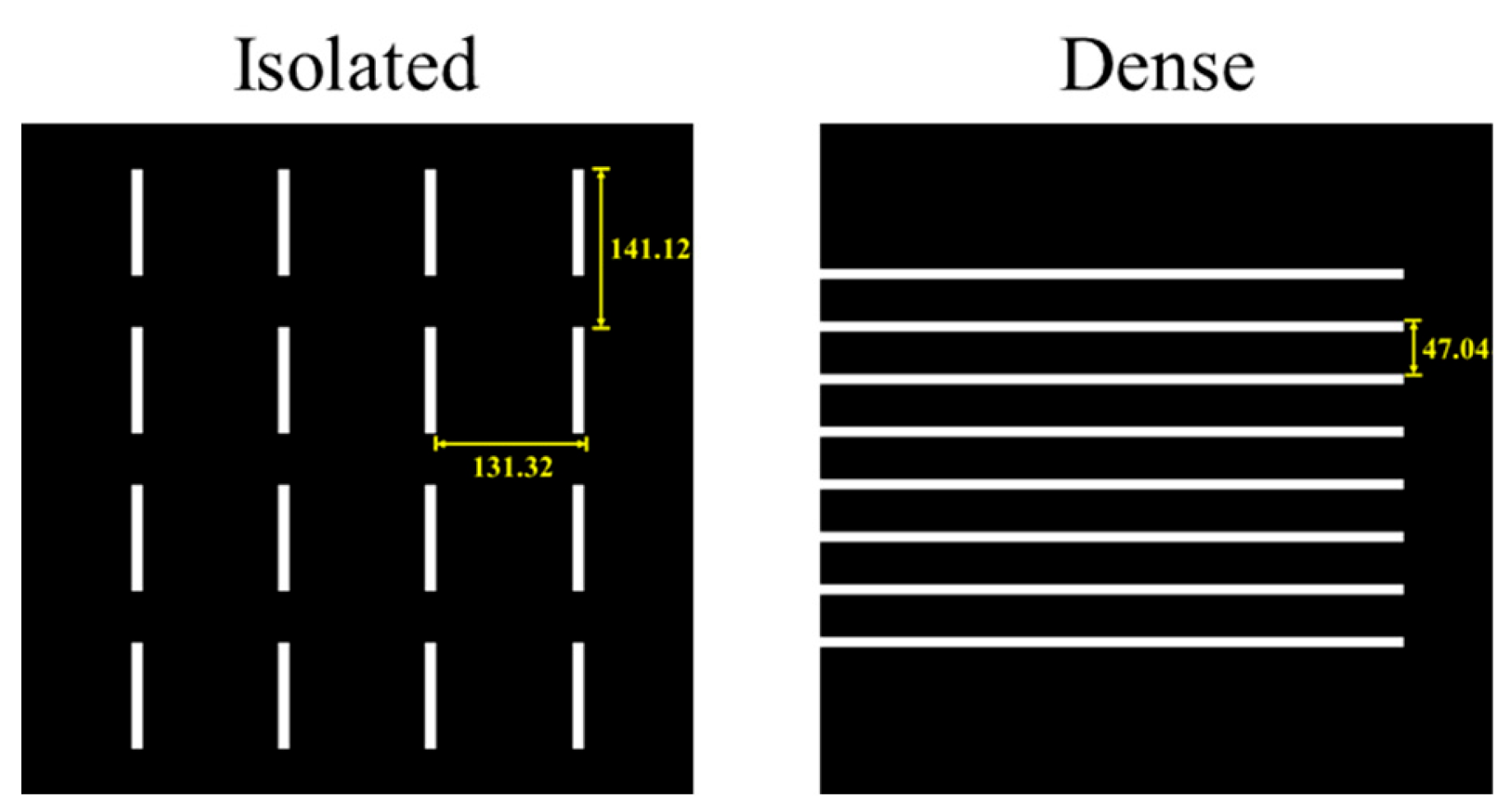
Figure 2.
Spin curve of center thickness versus spin speed. The model agrees with the Allresist datasheet value of 0.20 μm at 4000 rpm [55] and follows the expected Meyerhofer evaporation scaling (n = 0.5–0.7) [37], confirming the Emslie–Bonner–Peck viscous flow law [36].
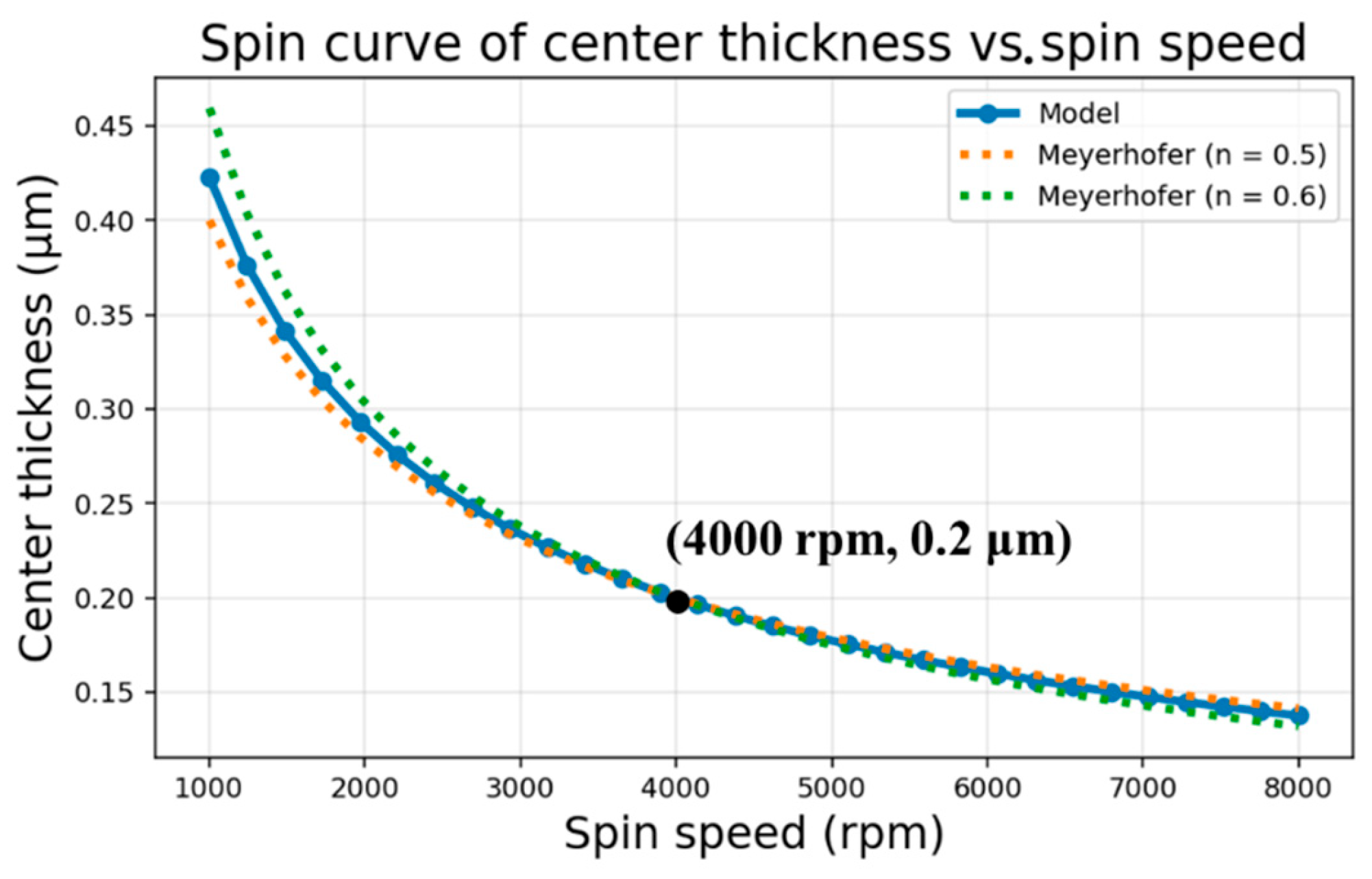
Figure 3.
Radial thickness profile at 4000 rpm. The empirical model match the central area with the Bornside solution [56] and agrees with both the mid-radius depression and rim thickening, as observed by reported edge-bead excess [57]; residual deviations can be corrected by data assimilation techniques.
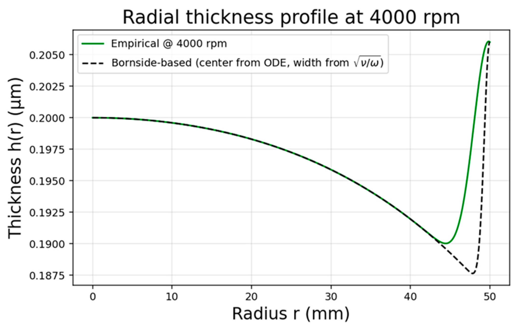
Figure 4.
Schematic of 3D level-set etch modeling. Interface: ; interior: . The evolving zero-level set captures anisotropic etch progression.
Figure 4.
Schematic of 3D level-set etch modeling. Interface: ; interior: . The evolving zero-level set captures anisotropic etch progression.
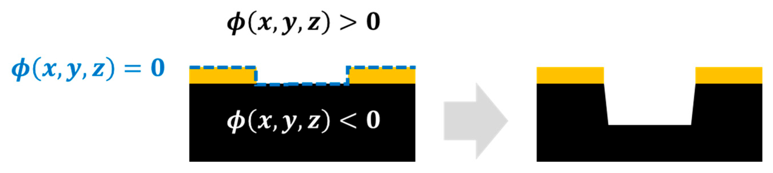
Figure 5.
Simulated 3D RIE topography.
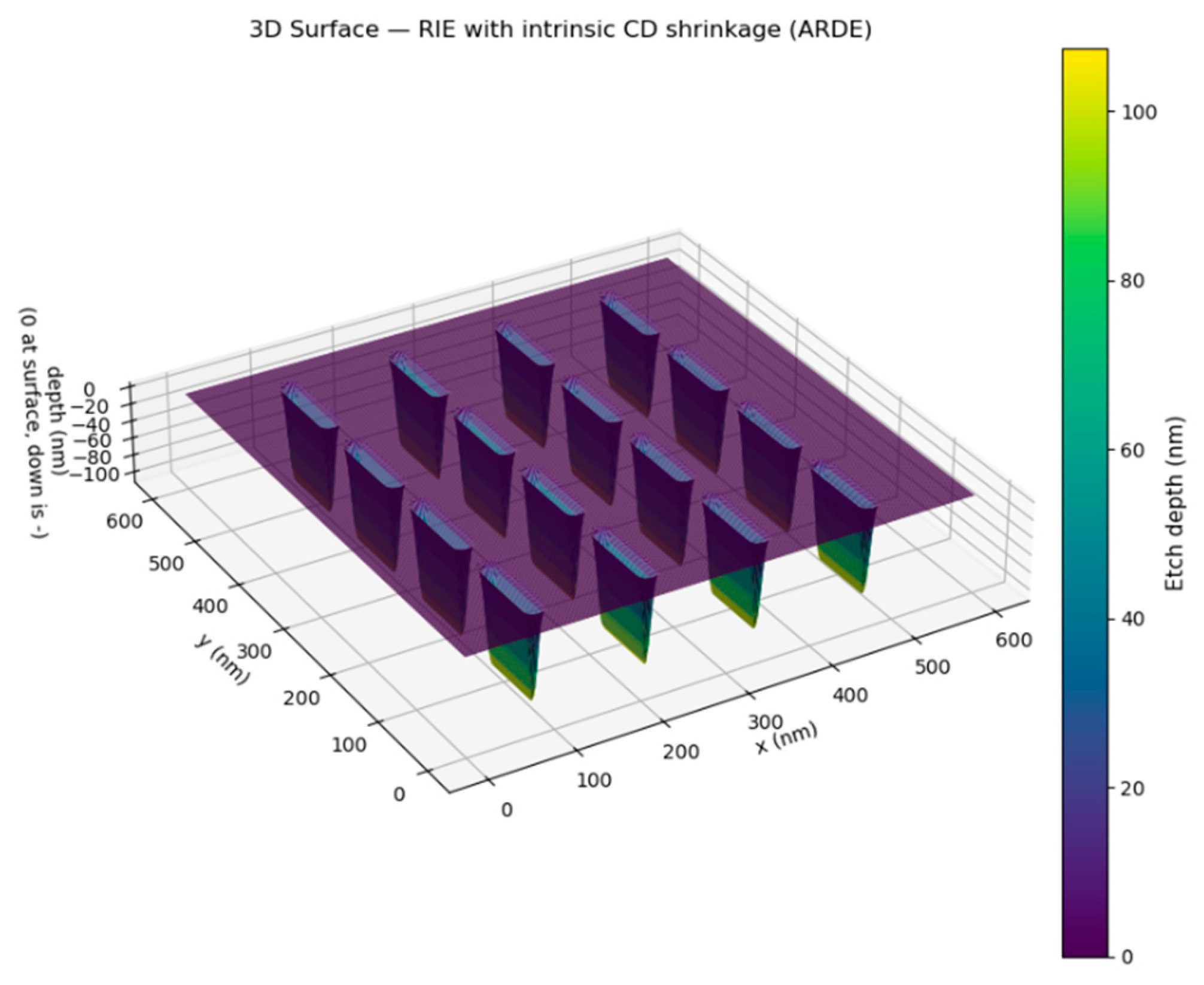
Figure 6.
Simulated resist thickness map at 4000 rpm for a 100 mm wafer (left). The automated algorithm selects the optimal 600 nm × 600 nm window near a 50 mm radius (marked in red), and the corresponding local thickness sub-map (right) confirms <0.1 nm variation across the tile.
Figure 6.
Simulated resist thickness map at 4000 rpm for a 100 mm wafer (left). The automated algorithm selects the optimal 600 nm × 600 nm window near a 50 mm radius (marked in red), and the corresponding local thickness sub-map (right) confirms <0.1 nm variation across the tile.

Figure 7.
Exposure map (left) and proximity-corrected dose (right) for isolated and dense layouts in the lower-bound case ().
Figure 7.
Exposure map (left) and proximity-corrected dose (right) for isolated and dense layouts in the lower-bound case ().

Figure 8.
Exposure map (left) and proximity-corrected dose (right) for isolated and dense layouts in the lower-bound case ().
Figure 8.
Exposure map (left) and proximity-corrected dose (right) for isolated and dense layouts in the lower-bound case ().
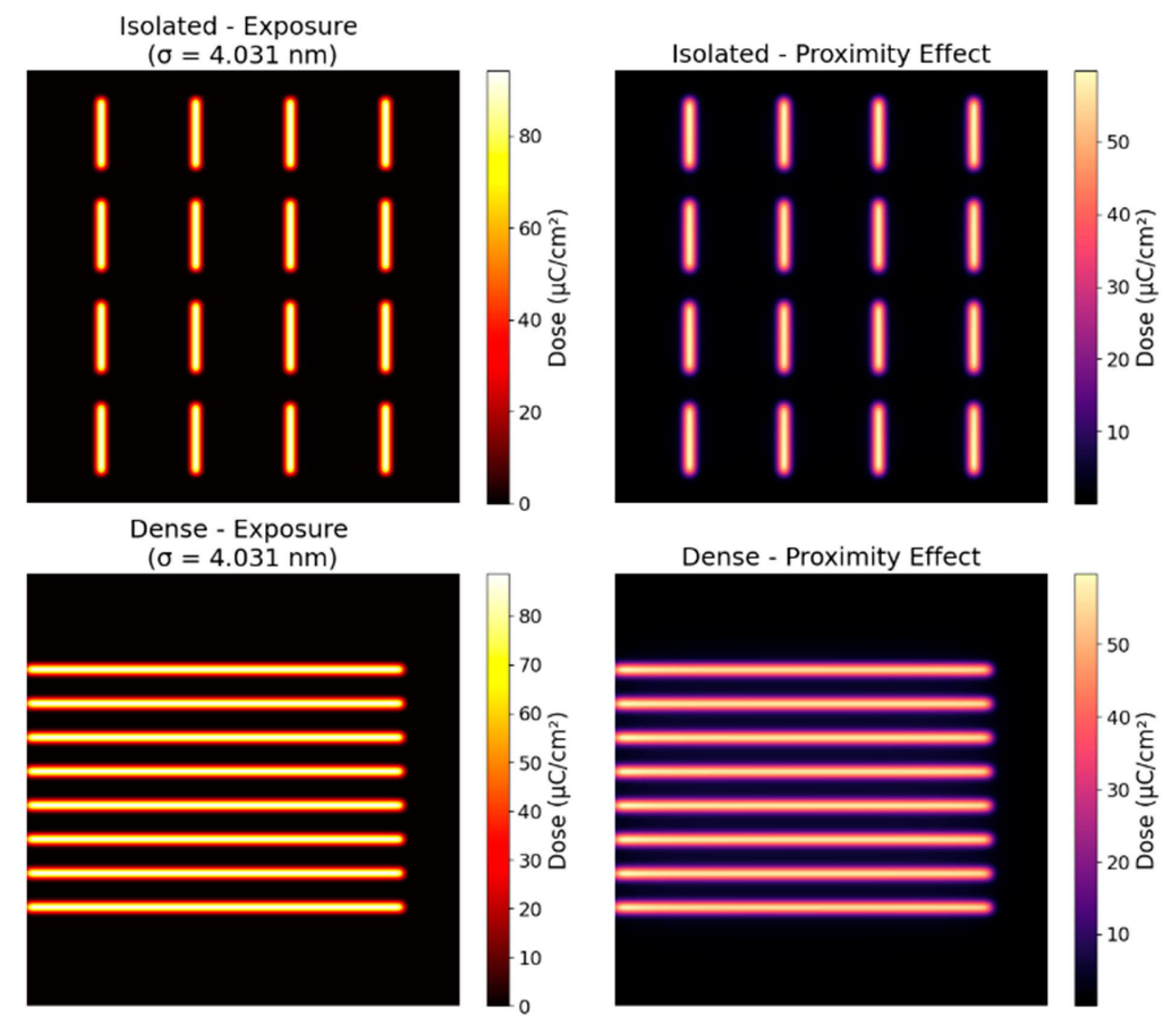
Figure 9.
Exposure map (left) and proximity-corrected dose (right) for isolated and dense layouts in the lower-bound case ().
Figure 9.
Exposure map (left) and proximity-corrected dose (right) for isolated and dense layouts in the lower-bound case ().
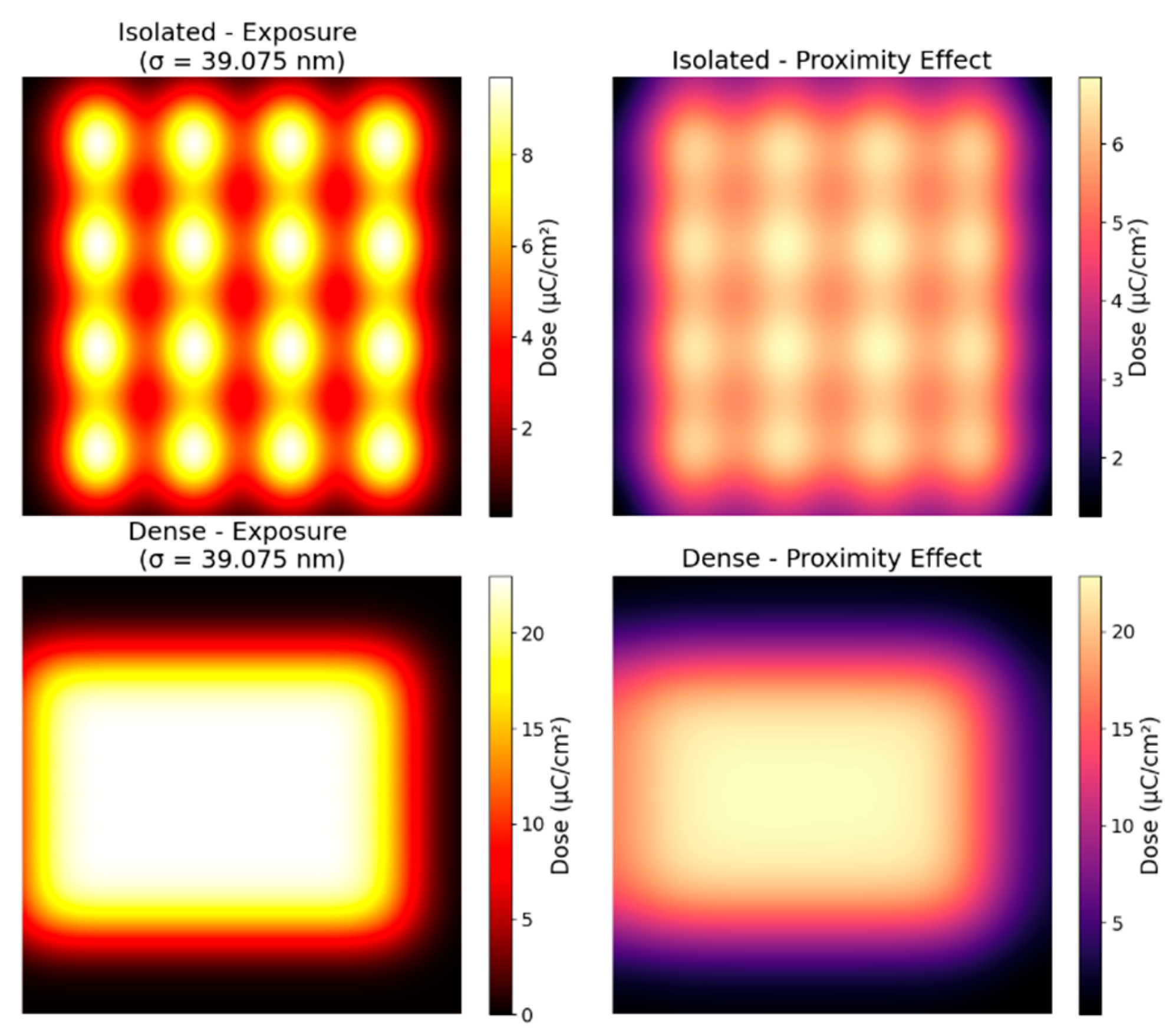
Figure 10.
ADI binary masks for isolated (left) and dense (right) layouts with spot size
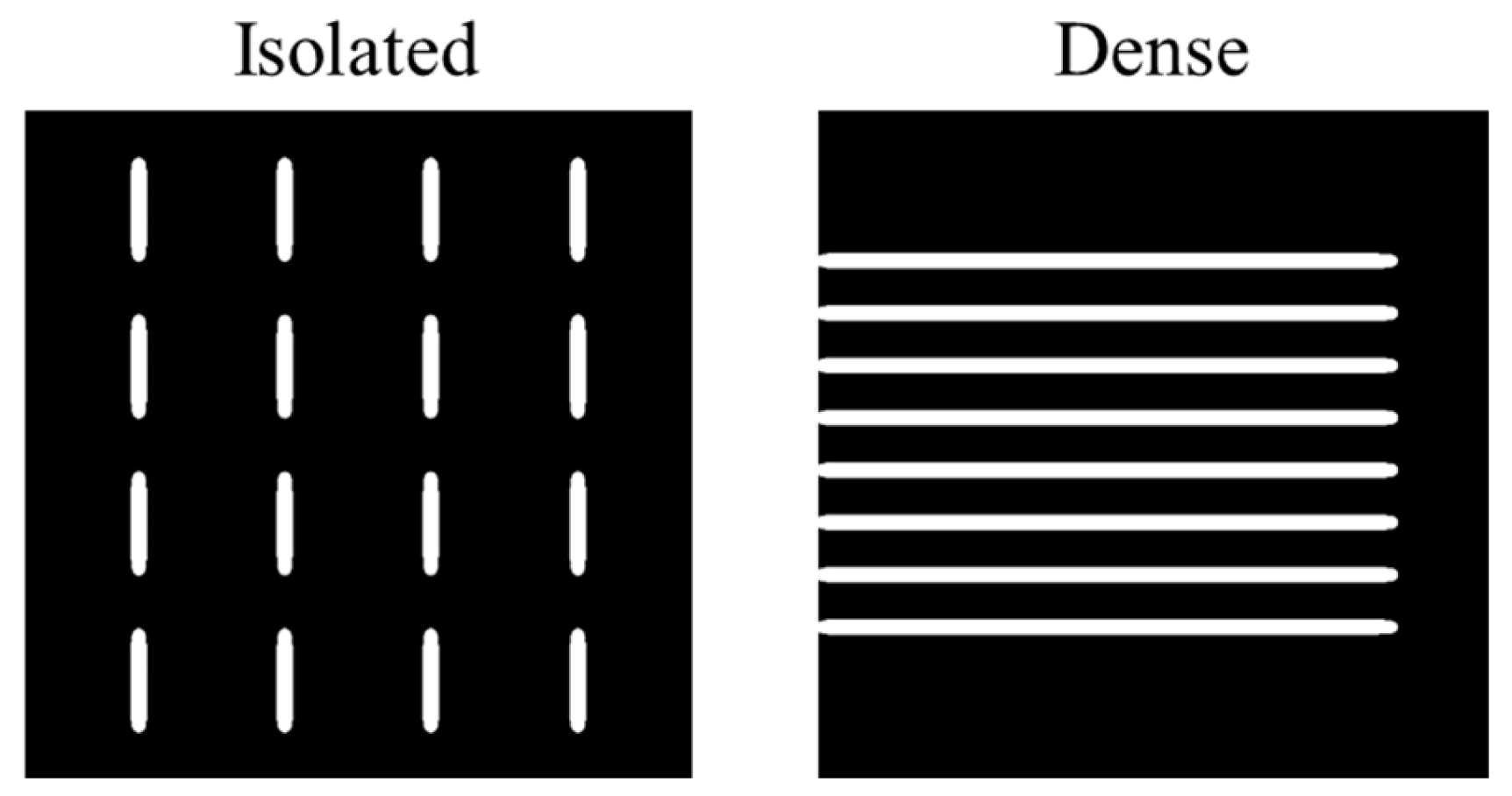
Figure 11.
Sensitivity of isolated pattern layout to PSF parameters. ΔCD (left) and LER (right) as functions of short-range Gaussian width σ (2–5 nm) and long-range backscattering radius γ (30–60 nm).
Figure 11.
Sensitivity of isolated pattern layout to PSF parameters. ΔCD (left) and LER (right) as functions of short-range Gaussian width σ (2–5 nm) and long-range backscattering radius γ (30–60 nm).
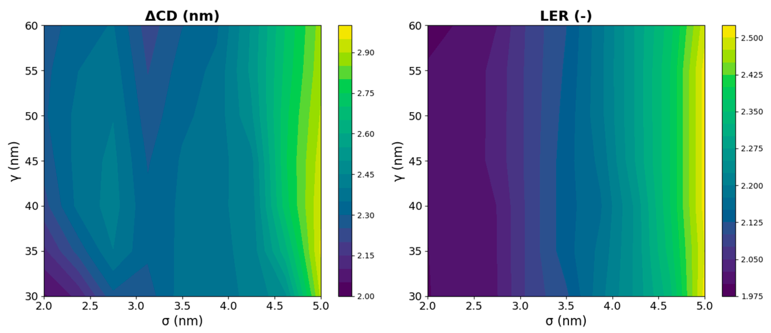
Figure 12.
Sensitivity of dense pattern layout to PSF parameters. ΔCD (left) and LER (right) as functions of short-range Gaussian width σ (2–5 nm) and long-range backscattering radius γ (30–60 nm).
Figure 12.
Sensitivity of dense pattern layout to PSF parameters. ΔCD (left) and LER (right) as functions of short-range Gaussian width σ (2–5 nm) and long-range backscattering radius γ (30–60 nm).
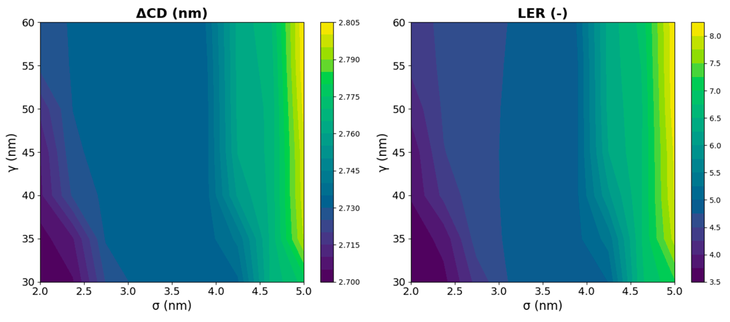
Figure 13.
AEI binary plot for isolated (left) and dense (right) layouts in a window ().

Figure 14.
Normalized CD shrinkage as a function of AR for four ARDE parameter sets.
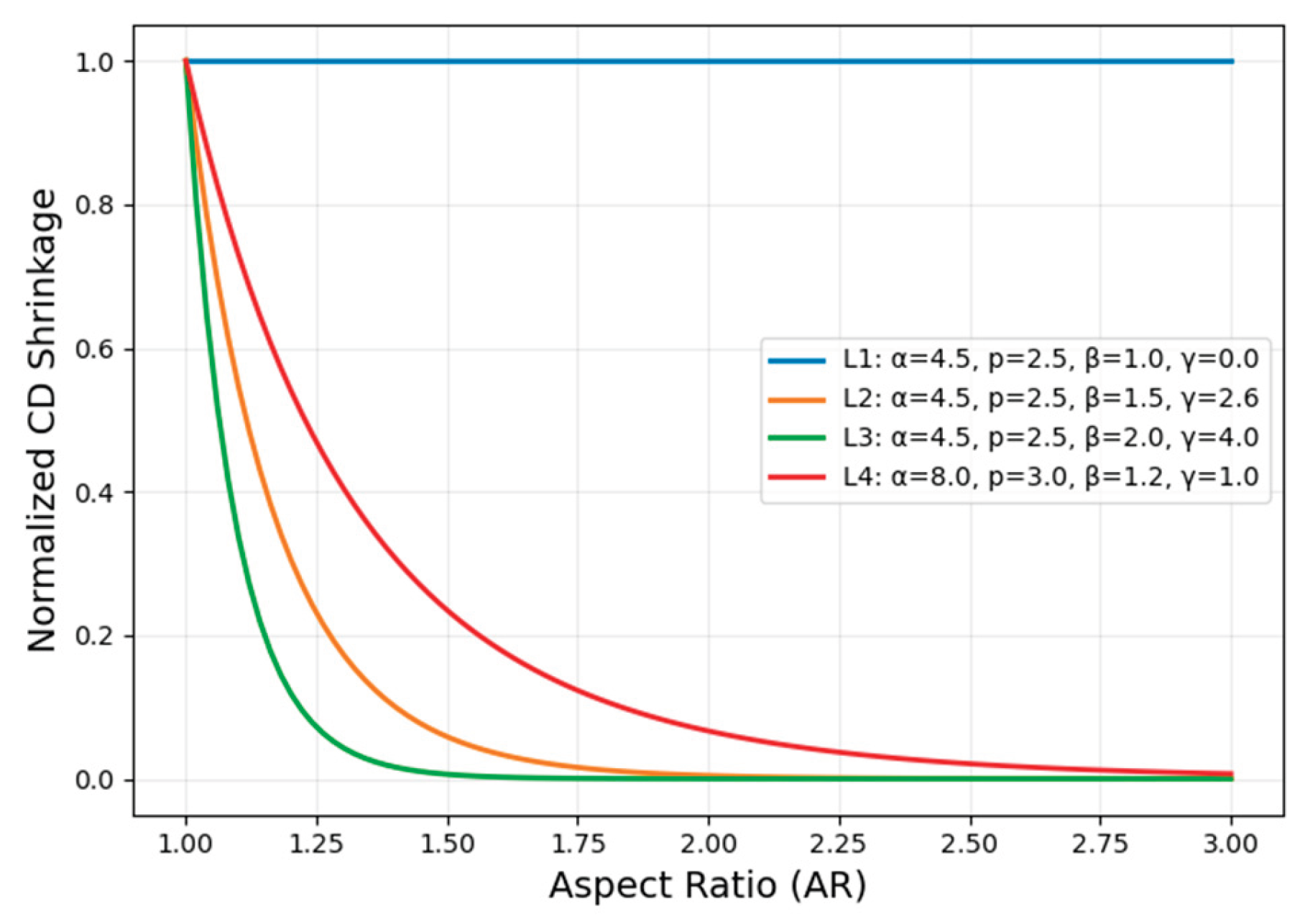
Table 1.
Parameters for simulation to derive from Lorentzian trajectory tracing.
| Condition |
|
|
|
|
|
|---|---|---|---|---|---|
| Numerical lower bound | 10 | 0.3 | 25 | -7.5 | 0.156 |
| Practical operating condition | 10 | 0.6 | 25 | -5.0 | 4.031 |
| Over-focused / proximity-dominated | 10 | 0.4 | 20 | -7.5 | 39.075 |
Table 3.
Comparison of PSF parameters used in this work versus published proximity-effect data for CSAR-62 on Si.
Table 3.
Comparison of PSF parameters used in this work versus published proximity-effect data for CSAR-62 on Si.
| Parameter / Behavior | This Work (30–40 keV) |
Published Range / Findings (CSAR-62 on Si) | Notes |
|---|---|---|---|
| Short-range Gaussian width ) | 4.031 nm | 2-5 nm [60,61] | Matches beam-blur / near-forward scattering. |
| Long-range backscattering radius (γ) |
45 nm | 20–60 nm for CSAR-62; 56–60 nm at 150 keV; lower voltages yield slightly shorter tails [54,60,61] | Ensures realistic backscatter tail length; avoids underestimation of proximity effect. |
| Relative amplitudes ) | Tuned to match beam current and substrate composition | Varies with resist thickness, Si substrate, and acceleration voltage [54,60,61] | Within reported amplitude ratios for semi-amplified resists. |
Table 5.
Comparison of ARDE parameters used in this work versus reported transport-limited RIE literature
Table 5.
Comparison of ARDE parameters used in this work versus reported transport-limited RIE literature
| Parameter / Behavior | This Work (30–40 keV) | Published Range / Findings (CSAR-62 on Si) | Notes |
|---|---|---|---|
|
for Si/Cl₂, Si/HBr RIE [62,63,64,65,66] |
Falls within typical transport-limited ARDE models; vertical etch decreases moderately with AR. | ||
| for sidewall passivation + reactant depletion [63,64,65,66,67] | Reflects stronger attenuation of lateral advance due to reduced off-angle ion flux and polymer deposition. | ||
| Lateral passivation factor | for HBr/O₂, CHF₃, CF₄ RIE [64,65,66,67] | Same γ as above; polymer deposition increases sidewall blocking at high AR. | |
| Ratio of lateral-to-vertical suppression | (stronger than vertical channel) | Lateral etch decreases 2–5× faster than bottom etch for AR > 2–3 [62,63,64,65,66,67] | Supports β > 1 and the presence of an additional exponential term. |
| Ion angular width | in ICP/RIE tools [68] | Matches measured ion energy–angle distributions. |
Disclaimer/Publisher’s Note: The statements, opinions and data contained in all publications are solely those of the individual author(s) and contributor(s) and not of MDPI and/or the editor(s). MDPI and/or the editor(s) disclaim responsibility for any injury to people or property resulting from any ideas, methods, instructions or products referred to in the content. |
© 2025 by the authors. Licensee MDPI, Basel, Switzerland. This article is an open access article distributed under the terms and conditions of the Creative Commons Attribution (CC BY) license (http://creativecommons.org/licenses/by/4.0/).
Copyright: This open access article is published under a Creative Commons CC BY 4.0 license, which permit the free download, distribution, and reuse, provided that the author and preprint are cited in any reuse.


