
Submitted:
12 November 2025
Posted:
17 November 2025
You are already at the latest version
Abstract
NanoArduSiPM is a compact, all-in-one particle detector designed to integrate scintillation-based detection with online and local signal processing. Building on previous generations of the ArduSiPM (Architected Detection Unit for Silicon Photomultipliers) technology, this third upgrade introduces a significant miniaturization of the system while enhancing performance. The detector combines a Silicon Photomultiplier (SiPM) with a System-on-Chip (SoC) architecture, allowing signal acquisition and processing and data transmission without the need for external units. The analog front-end includes a low-noise amplifier, a fast discriminator and a peak-hold circuit, enabling precise digitization of fast optical pulses. Signal reconstruction linearity and timing performance have been preserved despite the reduced form factor. The internal analog-to-digital (ADC) converter is calibrated for accurate amplitude measurement and the costumed analog electronics, that precede the SoC, are sufficiently fast to resolve single photoelectrons in typical SiPM signals, ensuring compatibility with the SoC’s performance capabilities. Furthermore, by combining threshold scans and ADC spectrum measurements, the system reliably extracts photoelectron amplitudes and confirms the consistency of the analog and digital signal paths. In conclusion the compact design, firmware flexibility and embedded data handling make NanoArduSiPM suitable for deployment in space platforms, remote sensing applications and distributed radiation monitoring networks.
Keywords:
silicon photomultiplier
; SiPM
; radiation-tolerant
; scintillator
; SoC
; Microcontroller
; IoT
; space
1. Introduction
Over the past decades, solid-state sensor and microcontrollers development have transformed particle detection by making possible the creation of small and power-efficient devices capable of being exploited in a wide range of applications, from space missions to environmental monitoring. One of the most significant developments in this area has been the advent of Silicon Photomultipliers (SiPM) [1], which have taken the place of conventional photomultiplier tubes (PMT) by providing similar performance while being much smaller .
The ArduSiPM (Architected Detection Unit for Silicon Photomultipliers) [3] is a compact, high-performance architecture specifically developed for the precise detection and quantitative analysis of photonic signals acquired through silicon photomultipliers (SiPMs). These signals can originate from a broad range of physical processes and experimental environments, including scintillation in organic or inorganic materials, luminescence from biological or chemical systems, emissions from solid-state devices, radiation-induced light from astrophysical sources such as stars and cosmic particles, as well as nuclear medicine applications involving radiopharmaceutical tracers [20,21].
Originally implemented within the Arduino ecosystem, the architecture has since undergone a major evolution and no longer depends on Arduino boards or their development framework. The name ArduSiPM has been retained to preserve continuity, scientific recognition, and consistency across publications, outreach and product development, reflecting its transition from a prototype concept to a mature, scientifically validated detection system widely employed in ground-based and spaceborne research.
First introduced in 2014, ArduSiPM represented the first published realization of a complete particle detection and data acquisition system fully implemented on a single System-on-Chip (SoC) device [2]. This pioneering approach demonstrated that all key functions—from analog signal processing to digital counting and communication—could be integrated within a single low-power embedded platform. Its flexible SoC-based architecture proved both robust and future-proof, as anticipated at the time, enabling seamless migration to newer hardware generations without requiring a full redesign. This architecture anticipated several later implementations developed by other groups, confirming the foresight and generality of the original approach [5,6,7,8,9,10,11].
The SoC enables real-time edge computing, eliminating the need of an external data acquisition system. The microcontroller’s internal peripherals such as analog-to-digital converters (ADC), timers, and communication interfaces allow ArduSiPM to perform advanced functions, including signal processing, event counting, histogram generation, and threshold scans. Meanwhile, the SiPM provides high gain, fast response, and single-photon detection capabilities, making it ideal for measuring scintillation light from ionizing radiation [4].
The ArduSiPM architecture, originally developed for particle detection with SiPMs, has also been employed in analytical chemistry applications for bio- and chemiluminescence measurements. In such setups, it provides single-photon sensitivity and a linear dynamic range suitable for quantitative luminescence analysis [17][18].
Building on previous technological developments, the third generation of the system, known as Nano ArduSiPM, was designed with a strong emphasis on miniaturization to enable its integration as a payload in a compact PocketQube-class satellite. The PocketQube platform follows a modular standard based on 1P units, where each unit is defined as a cube measuring 5 × 5 × 5 cm³. The “P” stands for “Pocket”, distinguishing it from the larger CubeSat “U” standard, based on 10 × 10 × 10 cm³ units. This extremely compact form factor makes Nano ArduSiPM particularly well-suited for low-cost, miniaturized space missions, where size, mass, and power consumption are critical constraints.In recent years, several compact CubeSat payloads dedicated to radiation monitoring have demonstrated the feasibility of highly integrated instruments for in-orbit operation, such as the RADMON aboard Aalto-1 [12], the CELESTA radiation experiment [13], and the commercial PiDOSE dosimeter developed for small satellite platforms [14]. Nano ArduSiPM follows this technological trend, introducing an all-in-one SoC-based detection system optimized for high performance and minimal volume, aimed at future PocketQube and CubeSat missions. A first in-orbit technology demonstration is foreseen in 2026, onboard Pilot-1, a 3P PocketQube satellite developed by CShark S.r.l., an Italian company specializing in NewSpace technologies and embedded systems.
2. The NanoArduSiPM Architecture
NanoArduSiPM, in Figure 1, is the third-generation development of the ArduSiPM technology designed to reduce the system size while preserving the performance and architecture of the previous version. It is based on the Microchip SAMV71 SoC [15], featuring a 300 MHz ARM® Cortex®-M7 processor. The processor package is 9 mm × 9 mm in size, enabling a more compact and lightweight design. The board layout has been designed using ultra-compact surface-mounted components. The resulting form factor is 42mm × 36mm × 3mm, with a total weight of 7 grams. NanoArduSiPM is designed for embedded applications, such as satellite payloads, where all operating voltages are provided externally by the Electrical Power System (EPS). The board integrates its own high-voltage generator for SiPM biasing, regulated by the onboard processor through a calibration curve specific to each device. A temperature sensor placed near the detector allows automatic bias adjustment to ensure stable operation under varying thermal conditions. The system includes a low-noise analog front-end, a fast discriminator with programmable threshold and a peak-hold circuit for accurate pulse amplitude digitalization. A comprehensive NanoArduSiPM architecture is presented in Figure 2. Signal acquisition and processing are performed entirely within the SoC. A key mechanical and integration feature of NanoArduSiPM is the adoption of a Flat Flexible Cable (FFC), enabling versatile placement of the detector board within compact or stacked satellite assemblies, with minimal impact on mass and volume. For the planned short-lifetime in-orbit demonstrations, selected commercial-grade FFCs are considered suitable, provided that materials with low outgassing and adequate thermal stability are used. Furthermore, a customized firmware has been developed for this version, enabling real-time and local data processing as well as onboard data compression. These features are particularly important for applications in space-based systems and embedded platforms, where limited bandwidth and power constraints require efficient data handling directly at the edge.
In summary, NanoArduSiPM preserves the all-in-one SoC-based architecture of its predecessor while mainly introducing design optimizations and firmware enhancing.
3. Overview of the Discrete Analog Front-End of NanoArduSiPM
This section presents the discrete analog system implemented in NanoArduSiPM, which operates alongside the SoC to ensure signal acquisition, amplification and discrimination. While the overall architecture remains consistent with the original ArduSiPM, the analog stages have been optimized for compactness and compatibility with the reduced form factor of the latest ArduSiPM version.
3.1. Low Noise Voltage Amplifier
A key element of the device readout is the low-noise amplifier (LNA), which amplifies input signals with minimal noise contribution. The LNA is based on a commercial high-speed operational amplifier, selected for its wide bandwidth of 500 MHz and low input-referred noise. Operating in inverting configuration, it offers sufficient gain while maintaining a fast response and low offset voltage. The amplifier is designed to preserve the integrity of short SiPM pulses, which typically last a few tens of nanoseconds. As in the original implementation, a cathodic readout configuration was chosen to carry the ground reference on the coaxial shield, improving noise immunity and allowing the SiPM to be placed remotely from the main board.
A miniaturized U.FL connector is used for this purpose, in line with the overall design goal of minimizing board size through compact, space-efficient components.
The analog output of the LNA is also available on a second U.FL connector, enabling external diagnostics and calibration while maintaining a low-profile layout.
The response of the amplifier to a fast input pulse is shown in Figure 3, where both input and output waveforms are reported.
3.2. Fast Discriminator
A high-speed single-ended comparator is used as a discriminator to detect pulses exceeding a programmable threshold. The selected component features sub-nanosecond time jitter and a propagation delay of approximately 7 ns, making it suitable for high-rate event detection. The discriminator design was first modeled and optimized through circuit-level simulations, and later refined and validated through laboratory measurements on prototype boards. Achieving the targeted performance required meticulous PCB layout optimization, as the NanoArduSiPM integrates high-speed digital logic tightly coupled with ultra-sensitive analog front-end stages. This mixed-signal environment imposes stringent constraints on grounding topology, signal routing, impedance control and power distribution, where even minor parasitic effects can significantly degrade timing accuracy and noise levels. Its performance improves upon the 6.67 ns time resolution required for Time of Arrival (ToA) measurements, which rely on the processor’s internal clock. The output is processed by the internal counter peripherals of the SAMV71 to register ToA events. Both the threshold level and pulse width of the discriminator are configurable via firmware. Furthermore, the discriminator output is routed to a test pin, enabling synchronization with external modules or coincidence logic with a second detection channel.
3.3. Peak Hold
To overcome the intrinsic limitations of microcontroller ADC sampling rates relative to the SiPM signal duration, NanoArduSiPM uses a peak-hold circuit. This analog block stretches the short SiPM pulse to a duration on the order of microseconds, allowing its amplitude to be sampled by the SoC 12-bit ADC running at 2 MSPS. A programmable reset mechanism allows signal shaping to be adapted to the scintillator and application-specific requirements. While this introduces a moderate dead time of typically a few microseconds, it remains compatible with event rates in the hundreds of kHz range, ensuring reliable performance in high-rate detection.
The peak-hold behavior is shown in Figure 6, where the output waveform follows the pulse maximum and maintains the amplitude long enough for the ADC to sample it.
3.4. Communication Interfaces
NanoArduSiPM inherits the full suite of communication interfaces available on the SAMV71 SoC. High-speed USB 2.0 is used for primary data transfer and configuration, supporting rates up to 480 Mbps. In addition, UART, I²C and CAN interfaces are provided for system integration in embedded applications. In the satellite configuration, a Serial Peripheral Interface (SPI) has been selected as the primary communication link between the detector and the satellite On-Board Computer (OBC), providing a deterministic and fully synchronous data exchange. This interface ensures robust timing behavior and predictable latency and its master–slave architecture naturally aligns with the hierarchical organization of on-board data handling systems. Such characteristics make SPI particularly suitable for payload subsystems requiring event-driven acquisition and deterministic synchronization with spacecraft timing signals, where asynchronous protocols such as UART may introduce variable delays and jitter. Conversely, the USB and wireless interfaces are primarily intended for ground-based use, supporting laboratory testing, calibration and stand-alone operation of NanoArduSiPM as a scientific or diagnostic instrument. Wi-Fi, Bluetooth, and LoRa connectivity are implemented as easily attachable add-on modules, providing versatile wireless access for configuration, data acquisition and distributed sensor networks during ground operations or field deployments. This dual-interface architecture enables a seamless transition from laboratory development to in-orbit deployment, minimizing hardware modifications while maintaining full access to configuration and diagnostic capabilities throughout all project phases. Altogether, these interfaces provide comprehensive configurability, operational flexibility and seamless integration in both terrestrial and space applications.
4. Assessing NanoArduSiPM: Characterization and Performances
The performance of NanoArduSiPM was thoroughly evaluated through a dedicated characterization [22]. This assessment aimed to verify improvements over previous versions while ensuring the device suitability for its target applications. Key aspects of the evaluation included the performance of the analog front-end and the characterization of SiPM signals amplitude.
4.1. Front-End Stage Linearity and Amplification
To evaluate the analog signal path preceding the digitization stage of the SAMV71 ADC, we characterized the behavior of the key front-end components, namely the low-noise amplifier and the peak-hold circuit.
Fast electrical pulses of 40 ns width and 5 ns rise time, representative of typical SiPM output signals, were injected with varying amplitudes to assess the linearity of the front-end response. As shown in Figure 7, the output of the LNA displays a linear dependence on the input signal amplitude. The regression fit yields a slope of , which is the amplification gain, with a correlation coefficient , indicating excellent linearity. The subsequent peak-hold stage, illustrated in Figure 8, also demonstrates a linear response with , and a fitted slope of , which again is the peak hold stage amplification gain. The observed baseline offsets can be compensated using the internal 10-bit DAC provided by the SAMV71, thereby restoring the baseline and improving the system’s effective dynamic range.
These measurements confirm the linearity and provides the amplification gain of the analog front-end, ensuring accurate amplitude amplification and processing in NanoArduSiPM.
4.2. ADC Calibration
The analog signal processing chain of NanoArduSiPM builds upon the architectural concept introduced over a decade ago in the first ArduSiPM developments. This design philosophy has proven remarkably forward-looking, anticipating the steady advances in mixed-signal integration and component miniaturization that now enable compact and efficient implementations. Compared to the ADCs integrated in earlier SoCs, modern converters offer significantly improved performance and calibration capabilities, with higher sampling rates, lower noise, enhanced linearity and advanced self-calibration. These advances have provided a major boost to the overall system performance and flexibility of the analog front-end. The SoC integrates two analog input paths to the ADC, each equipped with an independent Sample-and-Hold circuit, a 10-bit programmable DAC, and a Programmable Gain Amplifier (PGA), selectable via an internal multiplexer. For the scope of this characterization, only one analog channel is employed.
Offset compensation is achieved by adjusting the internal DAC to align the ADC baseline to zero. This calibration ensures that a 0 mV input corresponds to 0 ADC code, independent of the selected PGA gain. The ADC provides 12-bit resolution (4096 channels) over a 3.3 V range, while the sampling rate is 2 MS/s, allowing accurate digitization of signals.
To evaluate ADC linearity and the overall amplification chain, a 1 kHz pulse with 100 ns width was applied to the input. For each amplitude step, the corresponding ADC output was recorded and the linear response was confirmed through a regression analysis. In the case of PGA = 1, the DAC offset was set to 519 codes. The response is linear up to 650 mV, with a conversion factor of 0.077 mV/code and a negligible intercept, as shown in Figure 9.
4.3. ADC Channels Inefficiency
The NanoArduSiPM acquisition chain showed a very consistent behavior during testing, yet careful characterization revealed subtle imperfections in the ADC response, where certain channels exhibited localized inefficiencies. These appeared as systematic deficits in the number of recorded events under constant and uniform input conditions, indicating non-uniformities in ADC behavior. While such effects may have little impact on typical monitoring or counting applications, in nuclear spectroscopy even a small inefficiency on a single ADC channel translates into an unidentified gap in the reconstructed energy spectrum, potentially affecting spectral continuity and resolution.
To investigate this effect, an automated measurement procedure was implemented using rectangular input pulses of fixed width and frequency, with gradually increasing amplitude. The experimental setup used to characterize the ADC channel inefficiencies is schematically shown in Figure 10. It includes a PC-controlled waveform generator, the ADC acquisition chain and the NanoArduSiPM for data processing and histogram generation.
The acquired data were processed into histograms, where deviations from uniformity highlighted the presence of inefficient channels. A secondary measurement, performed with fixed-amplitude pulses, provided Gaussian distributions centered on the affected channels, allowing a quantitative estimation of the efficiency.
Results show that channel 507 exhibits approximately 80% efficiency compared to the expected counts, with the remaining events redistributed among neighboring channels. Despite this localized suppression, the total event count remains conserved, confirming that no data loss occurs. The deficit is visible in the histogram shown in Figure 11.
This behavior is consistent with limitations inherent to the ADC architecture, particularly related to linearity calibration errors caused by internal parasitic capacitances.
Furthermore, direct feedback from the Microchip ADC design team confirmed that the effect is intrinsic to the converter architecture. According to their analysis, the maximum linearity error occurs in two regions located approximately at one-eighth and seven-eighths of the reference scale. These non-linearities originate from parasitic capacitances within the ADC core and represent a technological limit associated with charge redistribution and noise constraints. In these regions, the integral non-linearity can reach amplitudes sufficient to cause local missing codes— precisely matching the anomalies observed experimentally. The affected areas were identified around ADC codes 512 and 3584 (0x202 and 0xE00), with device-to-device variations of about ±10 codes. Such agreement between the measured spectra and the manufacturer’s internal characterization conclusively demonstrates that the inefficiency is not caused by firmware or external circuitry, but is an intrinsic feature of the ADC design.
To mitigate these effects, dedicated firmware correction routines are being developed. The implemented method derives a channel-dependent efficiency map from calibration runs under uniform excitation. During acquisition, each ADC code is corrected via a lookup-based linearization table, redistributing counts according to the measured efficiency profile. This firmware-level compensation restores the expected flatness of uniform spectra and suppresses apparent gaps in reconstructed energy distributions without introducing artifacts. The correction can be periodically updated after recalibration, ensuring long-term uniformity and device-to-device consistency.
4.4. SiPM Signal Amplitude
Following the calibration of the threshold DAC and the Analog Front End ADC, the analysis of the signal amplitude was undertaken to correlate the number of detected photoelectrons with the measured signals. The threshold DAC, characterized by its fine resolution, serves as a precise instrument to link the signal amplitude to the corresponding number of photoelectrons fired. Given that the SiPM signal amplitude is quantized as an integer multiple of the single-cell response, lower amplitude signals, representing fewer simultaneous avalanches, are statistically more frequent.
A threshold scan was performed to investigate the count rate as a function of the discriminator level. Increasing the threshold progressively excludes lower-amplitude signals, effectively discriminating against smaller photoelectron coincidences. This process results in a characteristic stepwise count rate profile where each discrete drop corresponds to a specific number of photoelectrons.
The SiPM used for this setup was the Hamamatsu S13360-1350PE. In addition, to extend the dynamic range and resolve higher coincidence numbers, the experimental setup was enhanced by introducing pulsed LED illumination, controlled by a PicoQuant PDL 800-B [16]. The resulting threshold scan is shown in Figure 12, reveals the first four coincidence peaks clearly. The stepwise structure is consistent with the analytical model of multiple-coincidence dark noise in SiPMs presented in [19], which predicts the relative positions and amplitudes of the coincidence peaks observed in threshold scans.
By identifying the flex points in the threshold scan curve and converting these DAC code differences to voltage, the amplitude of a single photoelectron peak was determined to be
with the first peak located at approximately .
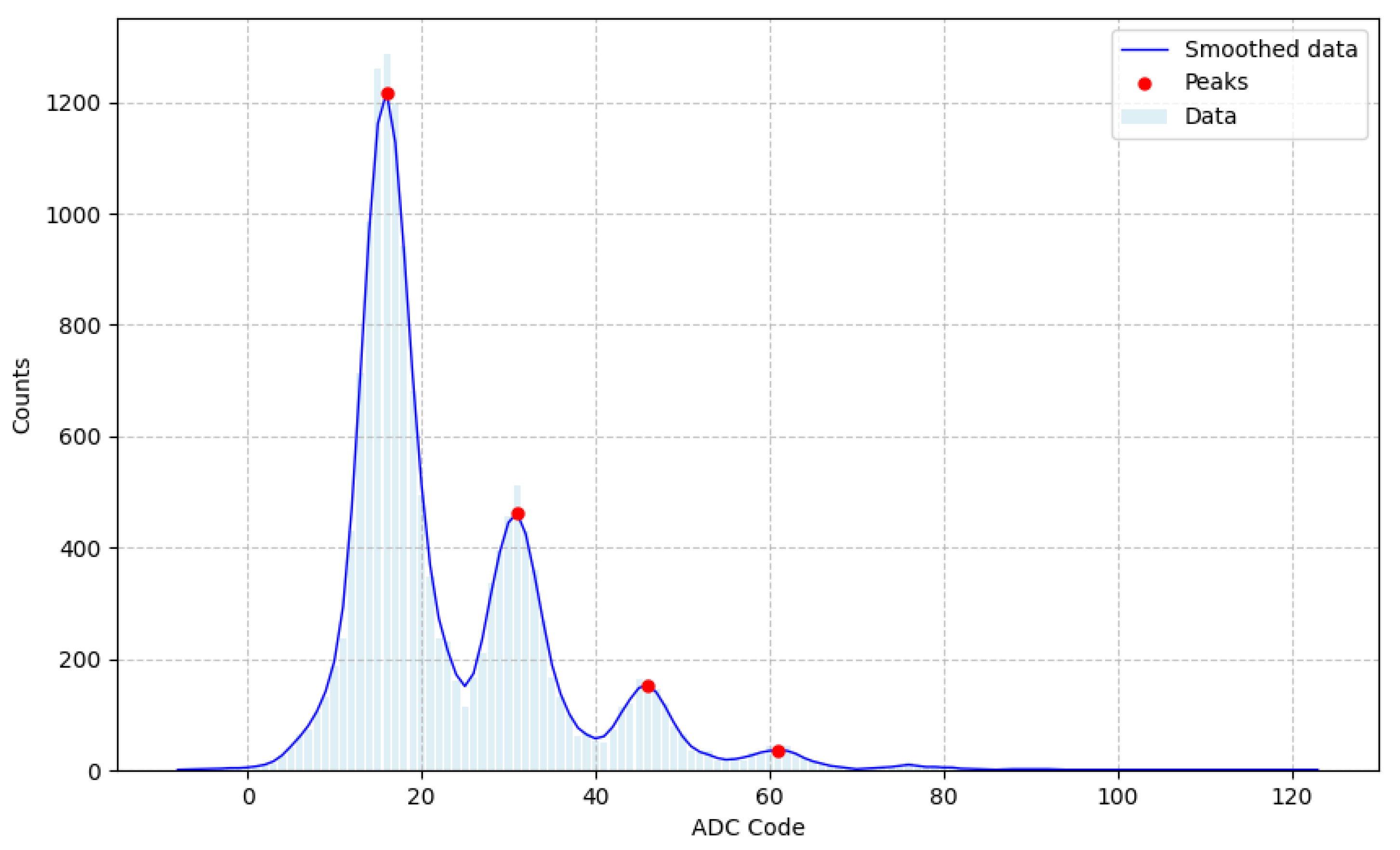
Furthermore the internal ADC of the NanoArduSiPM plays a crucial role in local data processing and quantification of photon counts. To cross-validate the threshold scan results, we also analyzed the spectrum obtained by digitizing the SiPM signal after amplification stages. Illuminated with low-intensity LED pulses under the same conditions, the ADC spectrum in Figure 13 exhibits up to the fourth coincidence peak. Applying a one-dimensional Gaussian filter to smooth the data and locate the peaks and converting the ADC codes to voltage , it yields a single-photoelectron amplitude of
with the first peak at .
The excellent agreement between the peak amplitudes measured via the threshold DAC scan and the ADC spectrum demonstrates the validity of the NanoArduSiPM’s signal processing costumed chain in resolving single photoelectrons. This analysis also confirms that NanoArduSiPM can reliably discriminate single and multiple photoelectron events, an essential feature for applications requiring precise photon counting and timing resolution.
5. Conclusions
NanoArduSiPM represents a significant step forward in the development of small, high-performance scintillation-based detectors. By combining a discrete analog front-end with a high-speed SoC, the system achieves full integration of acquisition, processing and communication functionality in an embedded and space-suitable form factor. The characterization results show that the analog chain has very good linearity, offering accurate signal amplification and digitization. The addition of a peak-hold stage effectively fixes the speed of SiPM signals, allowing for precise amplitude measurements with the SoC ADC. The system demonstrates the capability to resolve single photoelectrons both via threshold scans and direct ADC readout, validating its suitability for single-photon detection.
NanoArduSiPM’s small size, low power and edge computing capabilities, together with its customized firmware, further support a wide range of applications, from laboratory characterization to satellite payload operation and IoT. This technology, in conclusion, confirms that highly miniaturized devices can satisfy the level of performance required in demanding particle detection applications.
Author Contributions
Conceptualization, Valerio Bocci, Francesco Iacoangeli, Giacomo Chiodi, Luigi Recchia, Roberto Ammendola, Davide Badoni, Marco Casolino, Laura Marcelli, Gianmaria Rebustini, Enzo Reali, and Matteo Salvato; methodology, Valerio Bocci and Francesco Iacoangeli; software, Giacomo Chiodi, supervised by Valerio Bocci and Francesco Iacoangeli; hardware design, Luigi Recchia, supervised by Valerio Bocci; validation, formal analysis, investigation, and data curation, Valerio Bocci, Francesco Iacoangeli, Luigi Recchia, Giacomo Chiodi, and Alberto Merola, under the supervision of Valerio Bocci; writing—original draft preparation, Alberto Merola; writing—review and editing, Valerio Bocci, Francesco Iacoangeli, and Alberto Merola; visualization, Alberto Merola, guided by Valerio Bocci and Francesco Iacoangeli; supervision and project administration, Valerio Bocci; funding acquisition, Valerio Bocci, Davide Badoni, and Francesco Iacoangeli. The project was originally conceived by Valerio Bocci, who also led its coordination and scientific oversight. All authors have read and agreed to the published version of the manuscript.
Funding
The work was carried out within the LITE-SLPD experiment funded by the INFN (Istituto Nazionale di Fisica Nucleare), through its National Scientific Commission 5 (CSN5).
Informed Consent Statement
Not applicable.
Data Availability Statement
The data presented in this study are available on request from the corresponding author.
Use of Artificial Intelligence
Artificial intelligence (AI)-assisted tools were used in the preparation of this manuscript and in the development of analysis and control software. Specifically, AI tools aided in code structuring, in generating standard routines, and in refining the English language for clarity and fluency. The core scientific content, algorithmic logic, and interpretation of results were entirely developed, verified, and validated by the authors.
Acknowledgments
The authors would like to thank Cshark, represented by Alessandro Fanni (CEO), for his insight in recognizing the potential and usefulness of our concept, which led to its inclusion within the company’s satellite constellation. The authors also acknowledge Pietro Pavesi, working in collaboration with Cshark, for his contribution to the optimization of the PCB layout and component placement of the NanoArduSiPM.
Conflicts of Interest
The authors declare no conflict of interest.
References
- Gundacker, S.; Heering, A. The silicon photomultiplier: fundamentals and applications of a modern solid-state photon detector. Phys. Med. Biol. 2020, 65, 17TR01. [Google Scholar] [CrossRef] [PubMed]
- Bocci, V.; Chiodi, G.; Iacoangeli, F.; Nuccetelli, M.; Recchia, L. The ArduSiPM: a compact transportable Software/Hardware Data Acquisition system for SiPM detector. IEEE NSS/MIC 2014, 1–5. [CrossRef]
- Bocci, V.; Babar, A.; Badoni, D.; Casolino, M.; Chiodi, G.; Iacoangeli, F.; Kubler, D.; Marcelli, L.; Rebustini, G.; Reali, E.; Recchia, L.; Salvato, M. ArduSiPM technology: Compact and light all-in-one detectors for space application. Nucl. Instrum. Methods Phys. Res. A 2023, 1053, 168333. [Google Scholar] [CrossRef]
- Bocci, V.; Ali, B.; Chiodi, G.; Kubler, D.; Iacoangeli, F.; Masi, L.; Recchia, L. Cosmo ArduSiPM: An All-in-One Scintillation-Based Particle Detector for Earth and Space Application. Sensors 2024, 24, 3836. [Google Scholar] [CrossRef] [PubMed]
- Axani, S.N.; Conrad, J.M.; Kirby, C. The desktop muon detector: a simple, physics-motivated machine- and electronics-shop project for university students. Am. J. Phys. 2017, 85(12), 948–958. [Google Scholar] [CrossRef]
- Lavelle, C.M. Gamma ray spectroscopy with Arduino UNO. Am. J. Phys. 2018, 86(5), 384–394. [Google Scholar] [CrossRef]
- Topkar, A. et al. Development of Silicon Photomultiplier sensors using a 180 nm custom CMOS process technology. JINST 2020, 15, P03032. [Google Scholar] [CrossRef]
- Buonanno, L.; Di Vita, D.; Carminati, M.; Camera, F.; Fiorini, C. Miniaturized USB-powered multi-channel module for gamma spectroscopy and imaging. Rev. Sci. Instrum. 2021, 92(6), 063306. [Google Scholar] [CrossRef] [PubMed]
- Lee, J. et al. Comparison of Arduino Nano and Due processors for time-based data acquisition for low-cost mobile radiation detection systems. JINST 2022, 17, P03015. [Google Scholar] [CrossRef]
- Nicolae, M.Ş. et al. Remote Monitoring of Environment Radiation with Arduino Wemos and Geiger Counter Sensors. PQEMC-LF 2023, Craiova, Romania, 77–80. [CrossRef]
- Köhli, M.; Weimar, J.; Schmidt, S.; Schmidt, F.P.; Lambertz, A.; Weber, L.; Kaminski, J.; Schmidt, U. Arduino-Based Readout Electronics for Nuclear and Particle Physics. Sensors 2024, 24, 2935. [Google Scholar] [CrossRef] [PubMed]
- Gieseler, J. et al. Radiation monitor RADMON aboard Aalto-1 CubeSat: First results. Adv. Space Res. 2020, 66(1), 1–12. [Google Scholar] [CrossRef]
- Coronetti, A. et al. The CELESTA CubeSat in-flight radiation measurements and their comparison with ground facilities predictions. IEEE Trans. Nucl. Sci. 2024. [Google Scholar] [CrossRef]
- SkyFox Labs. SkyFox-Labs PiDOSE DCD Digital CubeSat Dosimeter. Available online: https://satsearch.co/products/skyfox-labs-pidose-dcd-digital-cubesat-dosimeter.
- Microchip Technology Inc. SAM E70/S70/V70/V71 32-bit Arm Cortex-M7 MCUs with FPU, Audio and Graphics Interfaces, High-Speed USB, Ethernet, and Advanced Analog. Complete Datasheet, 2023.
- PicoQuant. Available online: https://www.picoquant.com/products/category/picosecond-pulsed-sources/pls-series-sub-nanosecond-pulsed-leds#description (accessed on 10 April 2024).
- Calabretta, M.M.; Montali, L.; Lopreside, A.; Fragapane, F.; Iacoangeli, F.; Roda, A.; Bocci, V.; D’Elia, M.; Michelini, E. Ultrasensitive On-Field Luminescence Detection Using a Low-Cost Silicon Photomultiplier Device. Anal. Chem. 2021, 93(20), 7388–7393. [Google Scholar] [CrossRef] [PubMed]
- Martínez-Pérez-Cejuela, H.; Calabretta, M.M.; Bocci, V.; D’Elia, M.; Michelini, E. Super-Stable Metal–Organic Framework (MOF)/Luciferase Paper-Sensing Platform for Rapid ATP Detection. Biosensors 2023, 13(4), 451. [Google Scholar] [CrossRef] [PubMed]
- Bocci, V. A simple model for multiple coincidence SiPM dark noise. arXiv 2024. [Google Scholar] [CrossRef]
- Stagliano, M.; d’Errico, F.; Abegão, L.; Chierici, A. Silicon Photomultiplier: Current and Prospective Applications in Biological and Radiological Photonics. EPH - International Journal of Science And Engineering 2018, 4(4), 7–15. [Google Scholar] [CrossRef]
- Collamati, F.; van Oosterom, M.N.; De Simoni, M.; et al. A DROP-IN beta probe for robot-assisted 68Ga-PSMA radioguided surgery: first ex vivo technology evaluation using prostate cancer specimens. EJNMMI Research 2020, 10, 92. [Google Scholar] [CrossRef] [PubMed]
- Merola, A.; Bocci, V. (Advisor); Iacoangeli, F. (Co-Advisor). NanoArduSiPM characterization: a miniaturized high-speed photon detector for scintillation and photometry. M.Sc. Thesis, Sapienza University of Rome, 2025. [Google Scholar]
Figure 1.
Picture of the NanoArduSiPM board.
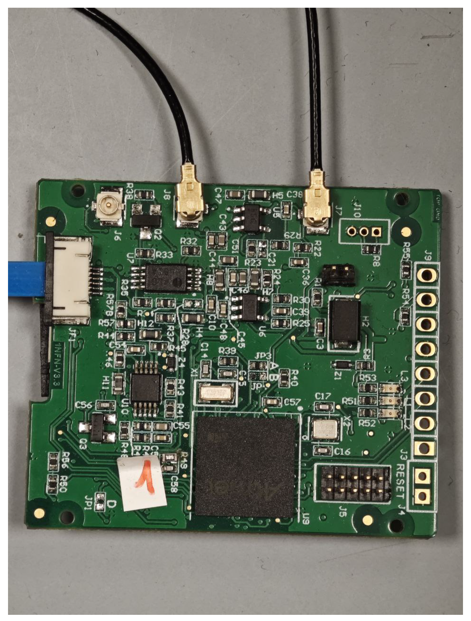
Figure 2.
Block Diagram of ArduSiPM technology. The implementation of most functions relies on the microcontroller’s internal peripherals. Depending on the specific application, analysis and interfaces can be configured accordingly.
Figure 2.
Block Diagram of ArduSiPM technology. The implementation of most functions relies on the microcontroller’s internal peripherals. Depending on the specific application, analysis and interfaces can be configured accordingly.
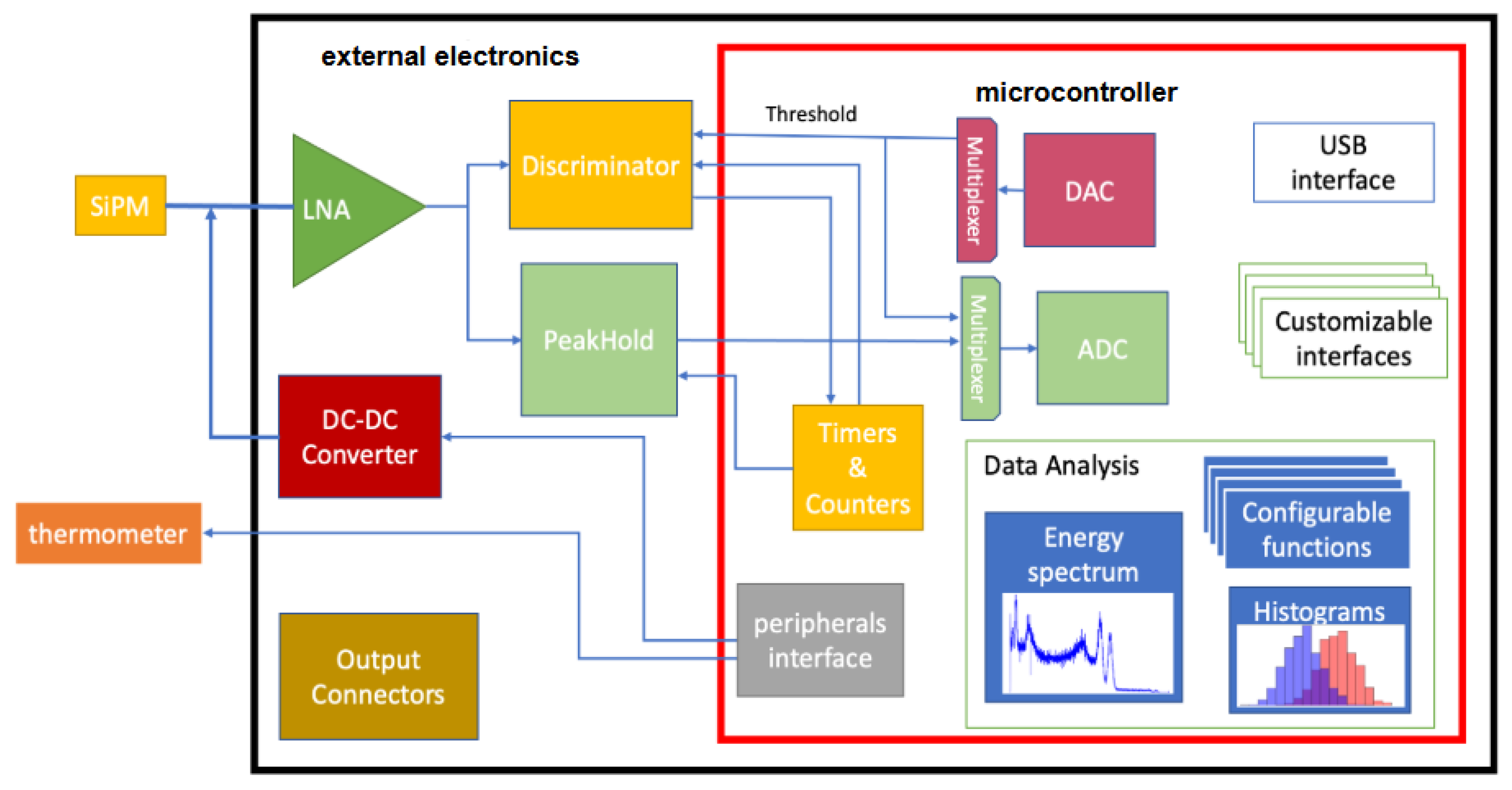
Figure 3.
Response of the LNA to an injected signal pulse studied using a 12-bit oscilloscope Lecroy WaveRunner HRO 64 Zi. The yellow waveform represents the input signal from a pulse generator. The pulse is 10 mV, with a width of 60 ns and a transient time of 5 ns. The fucsia signal is the output of the LNA in the standard configuration of the NanoArduSiPM.
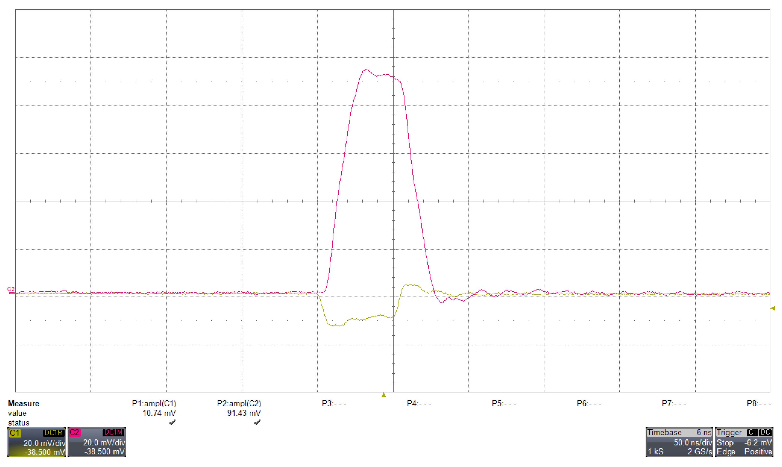
Figure 4.
In red, an injected pulse acquired with the oscilloscope from the analog output of NanoArduSiPM. The pulse is 10 mV, with a width of 60 ns and a transient time of 5 ns. The yellow signal is the output of the discriminator.
Figure 4.
In red, an injected pulse acquired with the oscilloscope from the analog output of NanoArduSiPM. The pulse is 10 mV, with a width of 60 ns and a transient time of 5 ns. The yellow signal is the output of the discriminator.
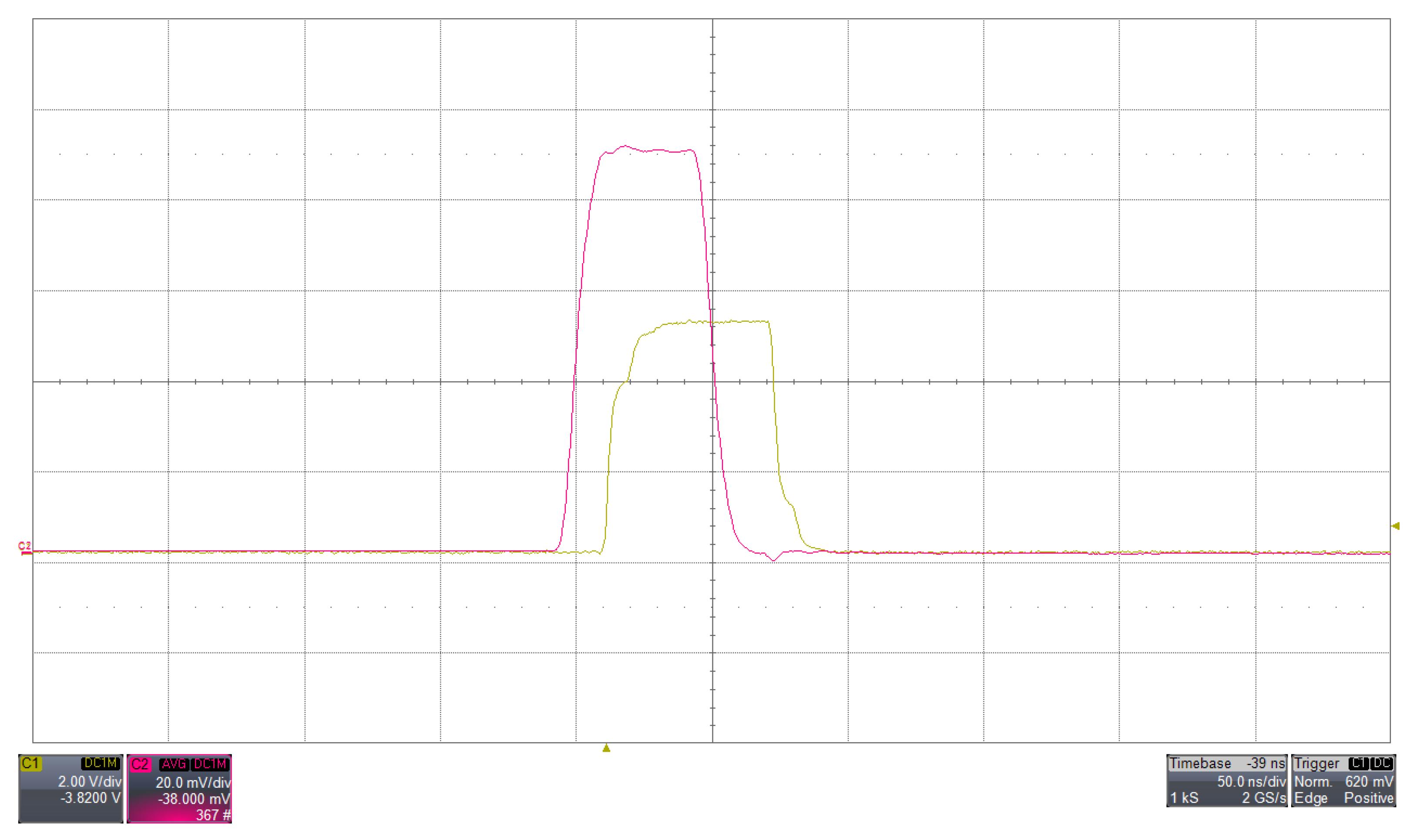
Figure 5.
In fuchsia, a SiPM signal acquired with the oscilloscope from the analog output of NanoArduSiPM. The yellow signal is the output of the discriminator.
Figure 5.
In fuchsia, a SiPM signal acquired with the oscilloscope from the analog output of NanoArduSiPM. The yellow signal is the output of the discriminator.
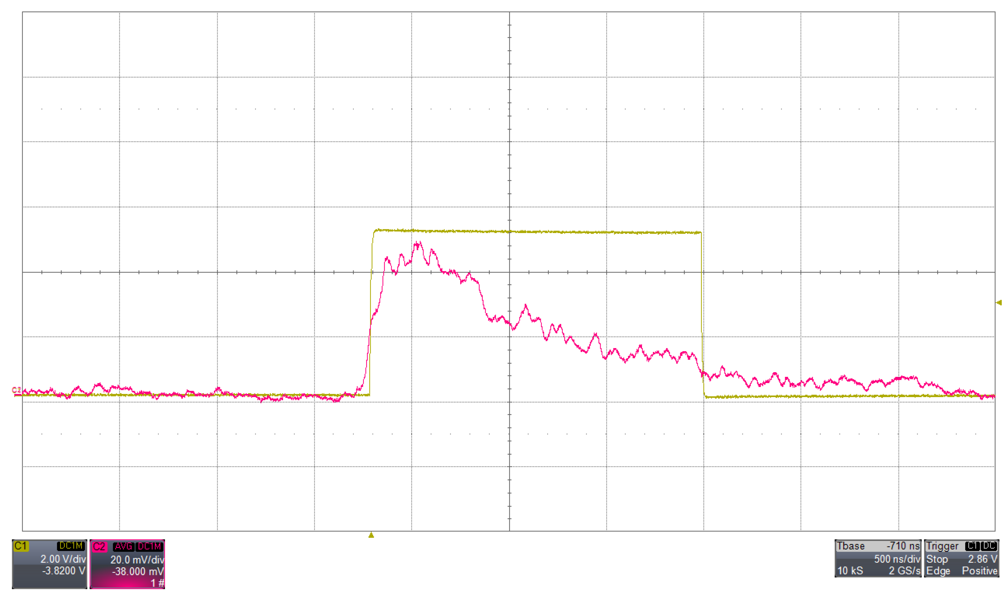
Figure 6.
In blue the peak-hold circuit output generated by a pulse signal. In fuchsia the analog output of NanoArduSiPM. . The waveforms are acquired with a oscilloscope LecroyWaveRunner HRO 64 Zi.
Figure 6.
In blue the peak-hold circuit output generated by a pulse signal. In fuchsia the analog output of NanoArduSiPM. . The waveforms are acquired with a oscilloscope LecroyWaveRunner HRO 64 Zi.
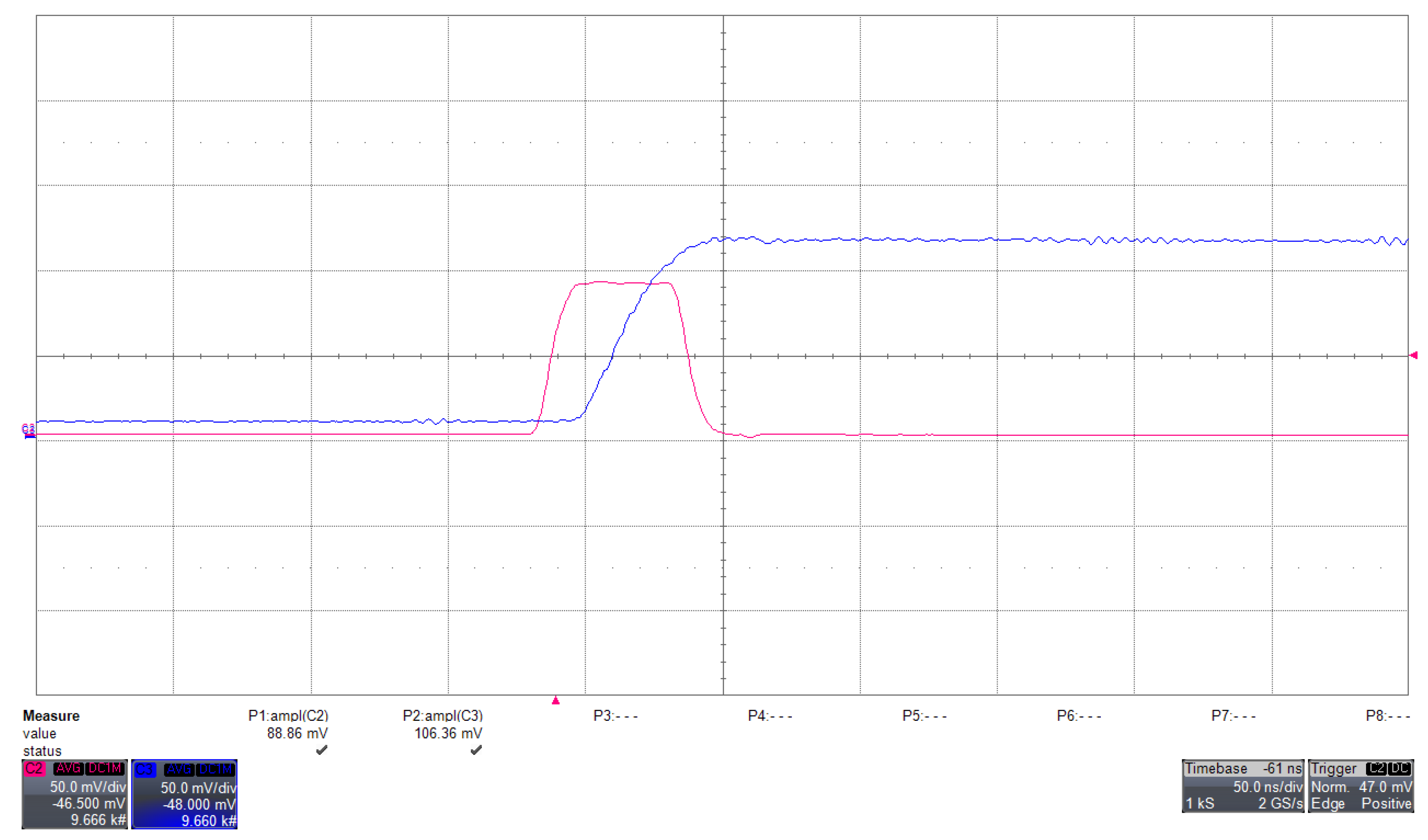
Figure 7.
Linear regression of LNA output as a function of the signal input amplitude. A fast 40 ns signal pulse, with 5 ns of transient time, is used as input to simulate a typical SiPM pulse.
Figure 7.
Linear regression of LNA output as a function of the signal input amplitude. A fast 40 ns signal pulse, with 5 ns of transient time, is used as input to simulate a typical SiPM pulse.
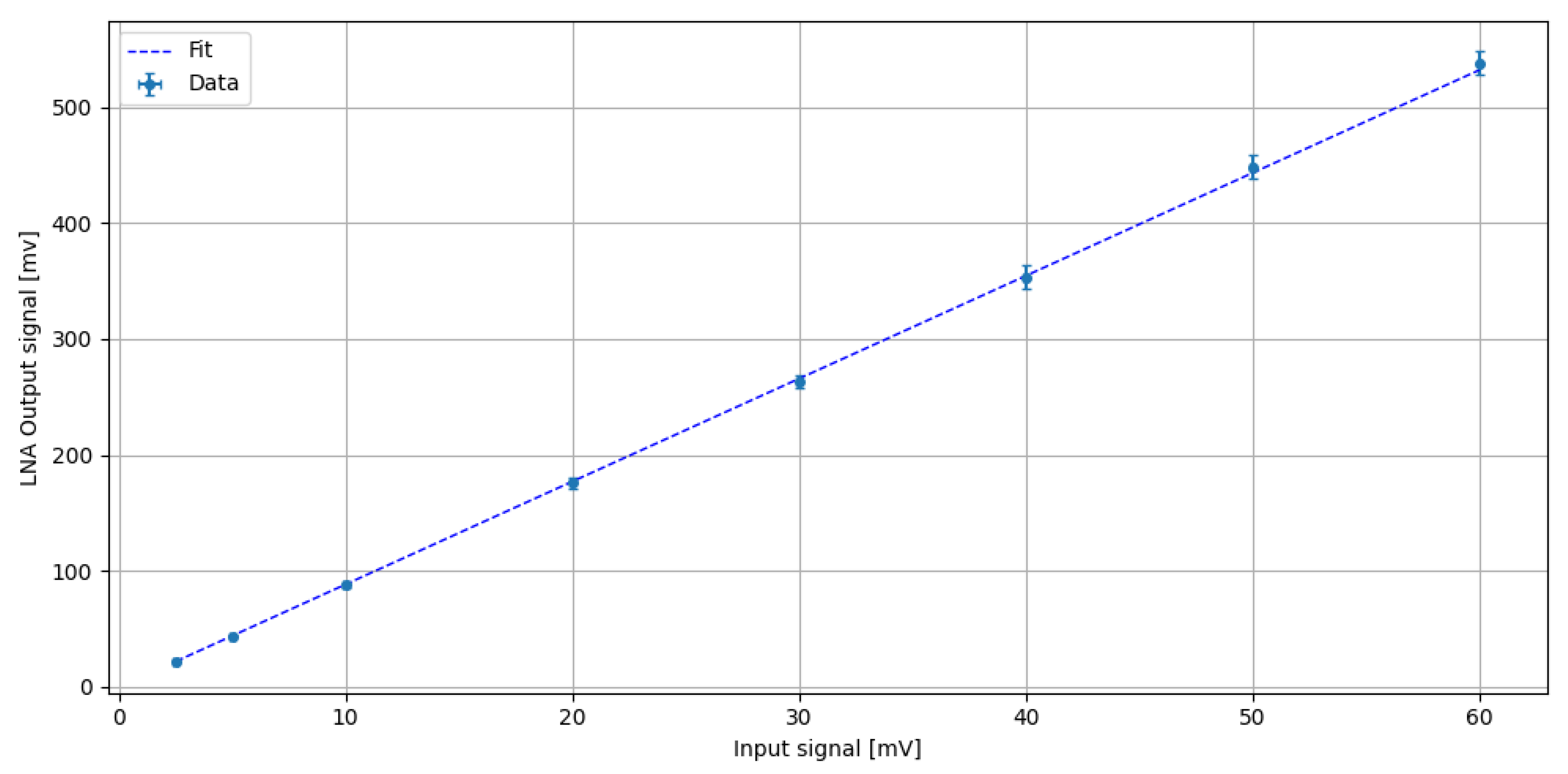
Figure 8.
Linear regression of peak hold output as a function of signal input amplitude. A fast 40 ns signal pulse, with 5 ns of transient time, is used as input to simulate a typical SiPM pulse. The offset is a feature of the peak hold circuit that depends on each individual device and can be compensated.
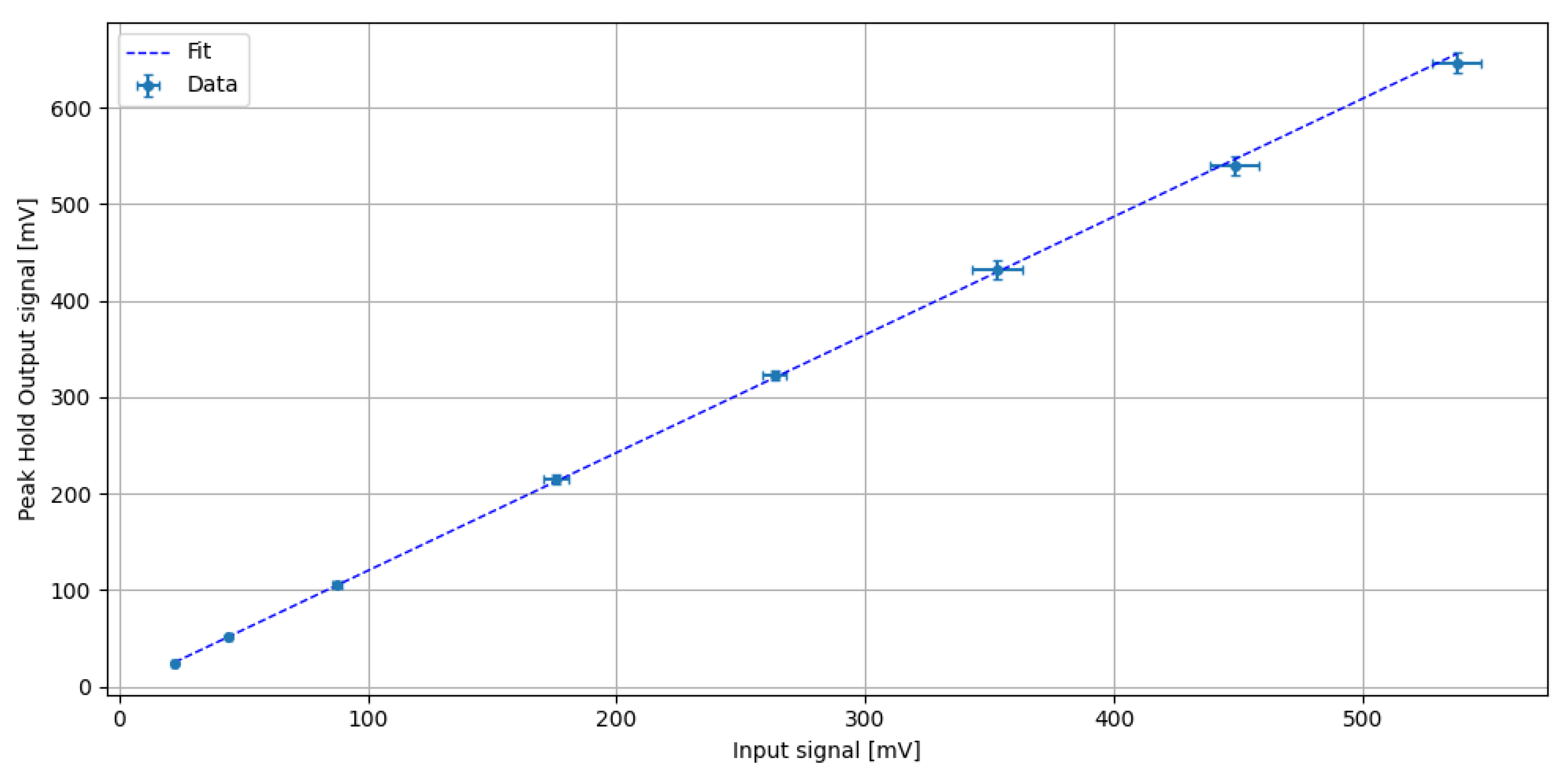
Figure 9.
Linear regression of ADC digital output as a function of signal input amplitude.
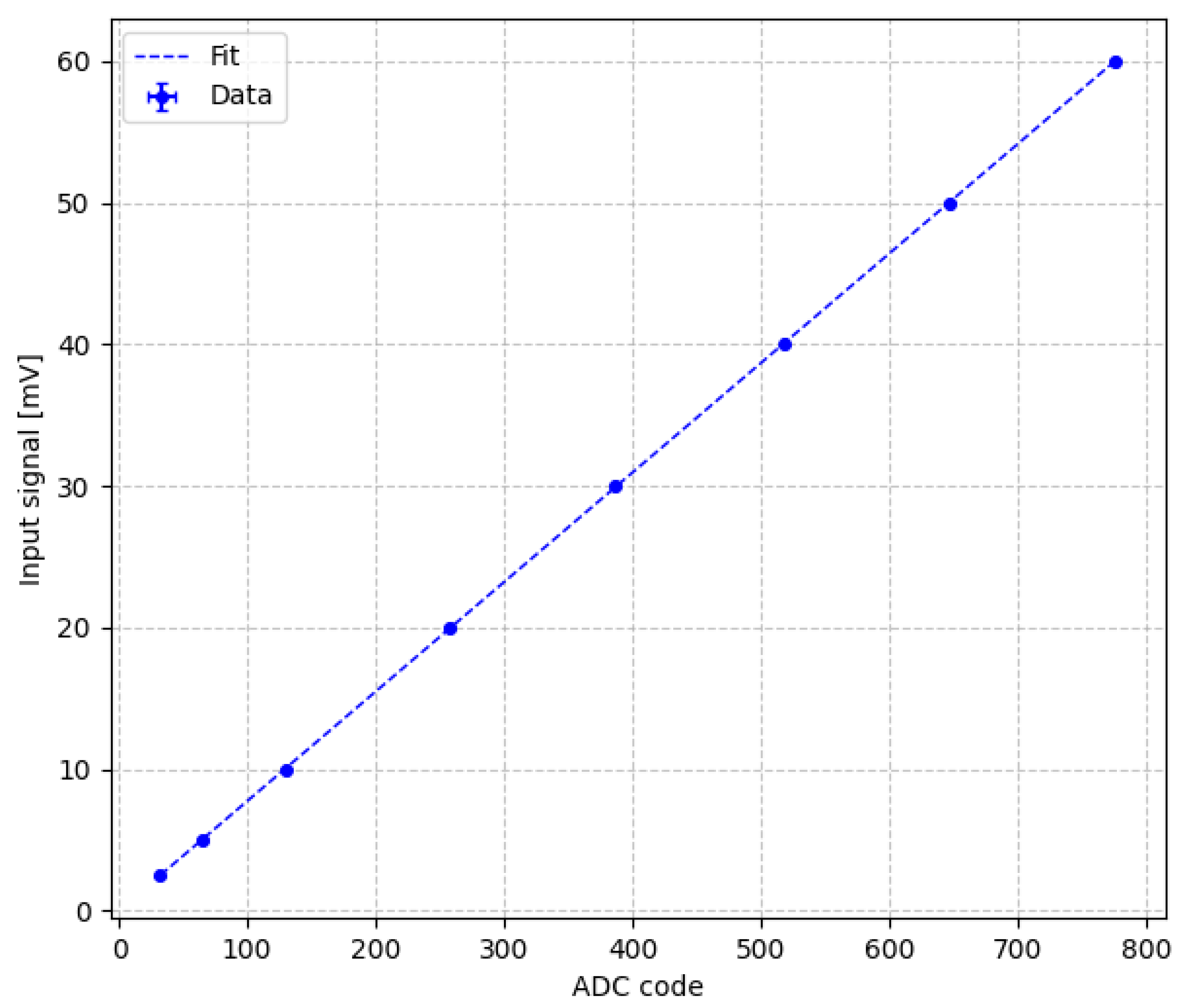
Figure 10.
Block diagram of the automated setup used to characterize ADC channel efficiency. The waveform generator produces rectangular pulses of controlled amplitude and frequency, acquired through the ADC and analyzed by the NanoArduSiPM.
Figure 10.
Block diagram of the automated setup used to characterize ADC channel efficiency. The waveform generator produces rectangular pulses of controlled amplitude and frequency, acquired through the ADC and analyzed by the NanoArduSiPM.
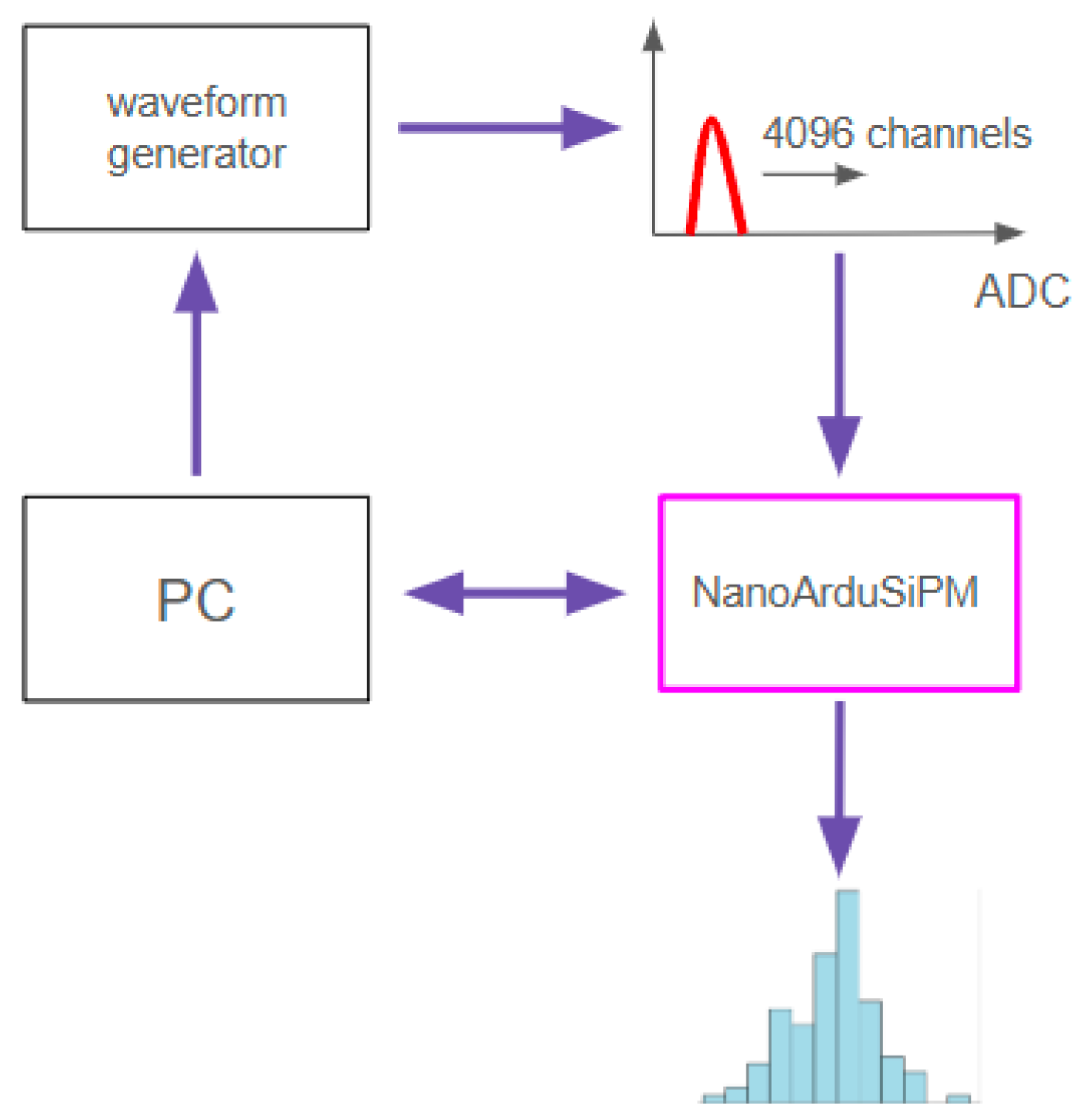
Figure 11.
ADC histogram obtained with a signal of 17.76 mV, PGA 4, frequency of 1 kHz and time width of 40 ns.
Figure 11.
ADC histogram obtained with a signal of 17.76 mV, PGA 4, frequency of 1 kHz and time width of 40 ns.
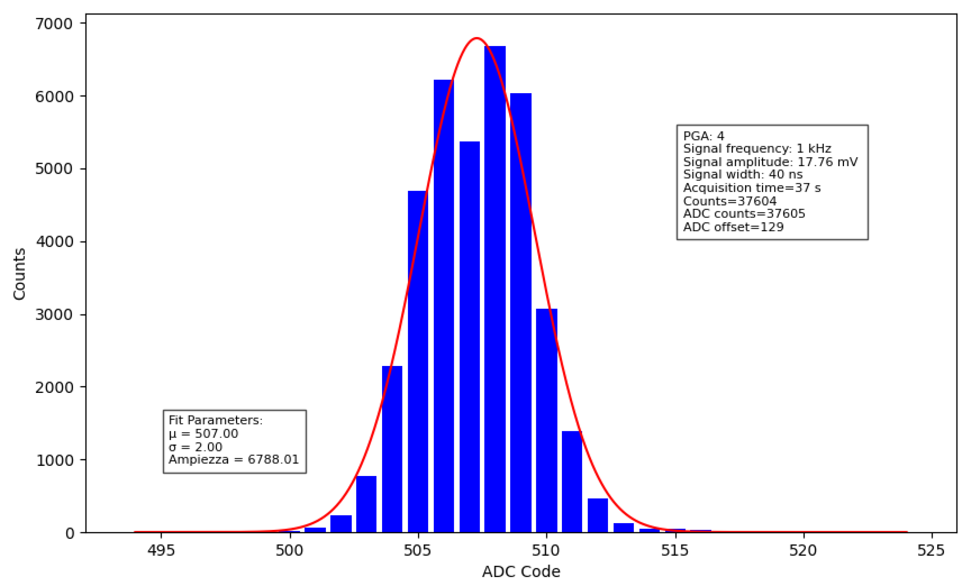
Figure 12.
Flex points at DAC codes 130, 310, 490, 670.
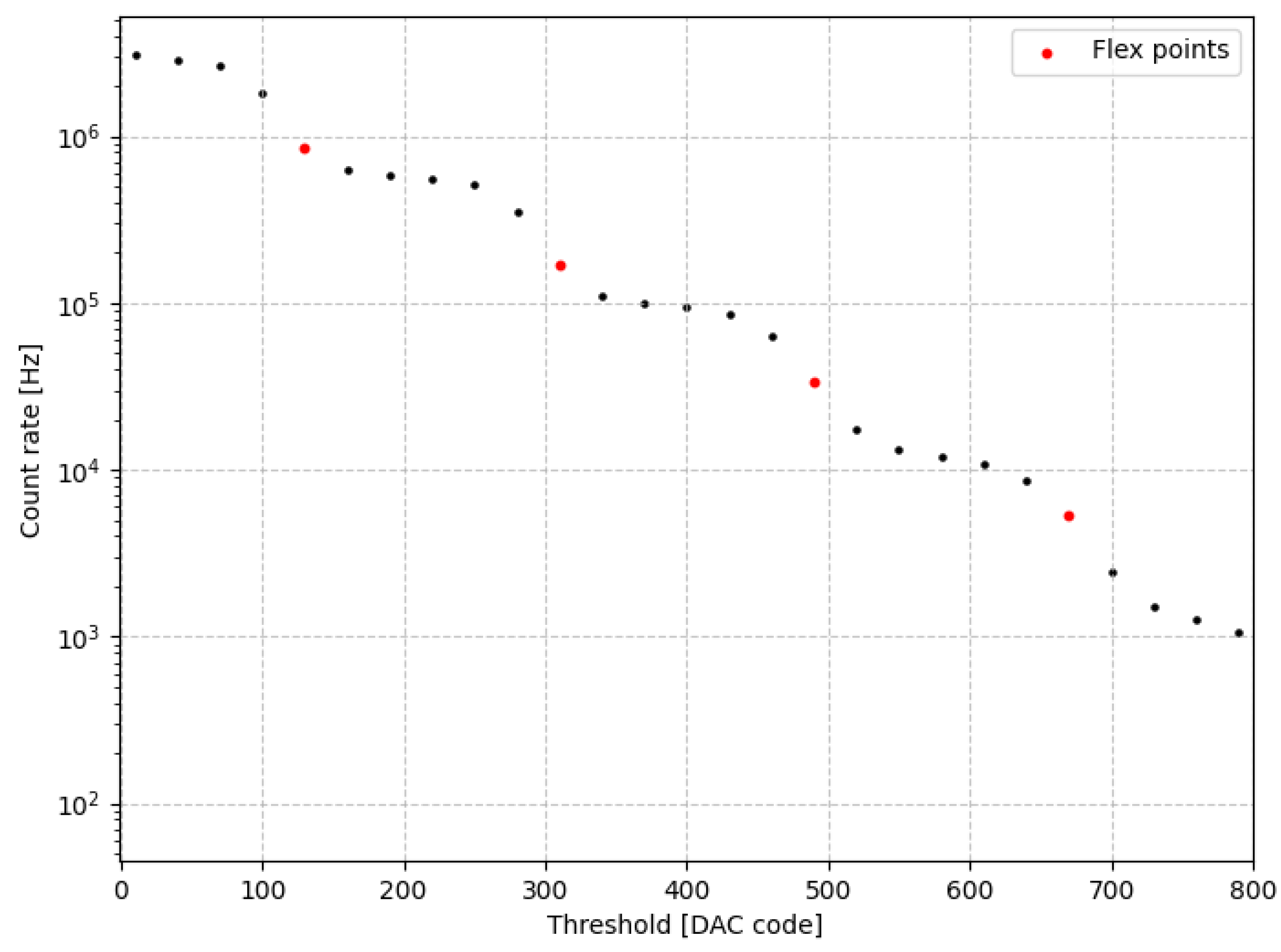
Figure 13.
Smoothed ADC spectrum with peaks at codes 16, 31, 46, 61.
Disclaimer/Publisher’s Note: The statements, opinions and data contained in all publications are solely those of the individual author(s) and contributor(s) and not of MDPI and/or the editor(s). MDPI and/or the editor(s) disclaim responsibility for any injury to people or property resulting from any ideas, methods, instructions or products referred to in the content. |
© 2025 by the authors. Licensee MDPI, Basel, Switzerland. This article is an open access article distributed under the terms and conditions of the Creative Commons Attribution (CC BY) license (http://creativecommons.org/licenses/by/4.0/).
Copyright: This open access article is published under a Creative Commons CC BY 4.0 license, which permit the free download, distribution, and reuse, provided that the author and preprint are cited in any reuse.


