Submitted:
10 November 2025
Posted:
11 November 2025
You are already at the latest version
Abstract
Reduced graphene oxide (rGO) exhibits strong anisotropic light absorption and high compatibility with photonic integrated chips, making it a promising material for implementing high-performance on-chip polarization-selective devices. The performance of rGO integrated waveguide polarizers is highly dependent on the waveguide geometry, and achieving optimal performance requires exploring a large parameter space, making conventional mode simulation methods computationally demanding. Here, we propose and demonstrate a machine learning framework based on fully connected neural networks (FCNNs) to map the dependence of the polarizer figure of merit (FOM) on the waveguide geometry. Once trained by using a small dataset of low-resolution mode simulation results, the FCNN framework can rapidly and accurately predict FOM values across a large structural parameter space with high resolution. Results show that this method can reduce overall computing time by more than 4 orders of magnitude as compared to the mode simulation methods, and achieve high prediction accuracy with an average deviation (AD) below 0.05. These results highlight the FCNN-based machine learning framework as an efficient tool for the design and optimization of rGO integrated waveguide polarizers.
Keywords:
waveguide
; polarizer
; graphene oxide
1. Introduction
Polarization control is fundamental to optical technologies, and polarizers serve as essential components that enable this function by allowing one polarization state to propagate while suppressing the orthogonal state [1,2,3,4]. Recently, on-chip integration of two-dimensional (2D) materials with strong anisotropic light absorption and broadband optical response has emerged as an attractive approach for realizing integrated polarizers with wide operation bandwidth and high polarization selectivity [3,4,5,6,7]. Particularly, reduced graphene oxide (rGO) has shown several unique advantages among various 2D materials [8,9,10,11]. First, it exhibits much stronger anisotropic light absorption than graphene oxide (GO), enabling enhanced polarization selectivity for rGO polarizers [10,12,13]. Second, rGO can be easily produced by reducing GO, retaining the benefits of solution-based and transfer-free methods for on-chip integration of 2D GO films and offering excellent compatibility with photonic integrated chips [14,15,16]. Finally, in contrast to GO that typically undergoes reduction under elevated temperatures and high optical powers, rGO exhibits significantly improved thermal stability and power endurance, making it particularly advantageous for high-power applications [8,11,16].
The performance of rGO integrated waveguide polarizers, quantitatively evaluated by the polarizer figure of merit (FOM), is highly dependent on the waveguide structural parameters [8]. In conventional methods, optimizing the structural parameters to achieve high FOM values requires extensive mode simulations across large structural parameter spaces. Such simulations rely on numerical mode simulation software and are computationally demanding, especially since accurate simulations of waveguides incorporating 2D materials require extremely fine meshing [17,18,19].
Recently, rapid advances in artificial intelligence (AI) technology are revolutionizing the modeling and design of optical devices [20,21,22,23]. Unlike conventional simulation approaches that depend on iteratively solving Maxwell’s equations, AI significantly enhances computational efficiency by constructing neural networks that directly map structural parameters to optical responses, thereby capturing underlying physical relationships [24,25,26,27]. This transformative paradigm offers broad applicability, demonstrating notable strengths in tackling complex design challenges and optimizing sophisticated photonic structures [21,23,28,29,30]. Up to now, AI-driven methods have achieved considerable success in designing diverse functional devices, including metasurfaces [24,31,32,33,34], nonlinear optical devices [35,36], electro-optic modulators [37], photodetectors [38,39,40], and quantum optical devices [41,42,43].
In this work, we propose a machine learning framework based on fully connected neural networks (FCNNs) to optimize the performance of rGO integrated waveguide polarizers. Trained by using a small dataset of low-resolution mode simulation results, the FCNN framework can predict the FOM values across a large structural parameter space with high resolution. Compared with traditional mode simulation methods, this approach not only reduces overall computing time by more than 4 orders of magnitude, but also achieves high prediction accuracy with an average deviation (AD) below 0.05. In addition, we construct nine training datasets with different sizes, and analyze the trade-off between improvements in prediction accuracy and the cost of building the training dataset. These results verify the effectiveness of the FCNN-based machine learning framework in efficiently designing and optimizing rGO integrated waveguide polarizers.
2. Device Structure
Figure 1a illustrates the schematic of an integrated waveguide polarizer based on a silicon photonic waveguide coated with a monolayer rGO film. The cross section of this hybrid waveguide is shown in Figure 1b, where W and H represent the width and height of the silicon waveguide, respectively, and n, k, and d represent the refractive index, extinction coefficient, and thickness of the rGO film, respectively. These parameters play a critical role in determining the performance of the rGO integrated waveguide polarizers.
rGO [44,45,46,47,48] can be derived from GO [4,6,49,50,51] through reduction processes that remove oxygen-containing functional groups (OFGs) such as hydroxyl, epoxide, carbonyl, and carboxylic groups [52,53]. In contrast to graphene, which has a low solubility, GO containing hydrophilic OFGs can be readily dispersed in water and processed in solution [14,54]. Recently, a solution-based, transfer-free method has been developed for on-chip integration of 2D GO films [12,13,54,55], which allows layer-by-layer film coating in large areas with precise control of the film thickness. The GO coated on integrated devices can be easily reduced to form rGO by using various methods, such as thermal reduction, chemical reduction, laser reduction, and microwave reduction [15]. During the reduction process, the restoration of sp2-hybridized carbon domains results in a decreased optical bandgap and changes in the material properties such as optical absorption and refractive index [8,11]. Different degrees of rGO reduction are achieved depending on the extent to which OFGs are removed. When the OFGs are completely removed and no residual groups remain on the carbon network, the bandgap approaches zero, and the material properties closely resemble those of graphene [52,56]. Therefore, the reduction of GO into rGO also provides an appealing route for mass-producing graphene-like materials through solution-based processing [57,58].
The hybrid waveguide shown in Figure 1a exhibits significantly stronger light absorption for transverse electric (TE, in-plane) polarization than for transverse magnetic (TM, out-of-plane) polarization. This behavior arises from the interaction between the evanescent field of the silicon waveguide and the 2D material film, which possesses strong anisotropy in its light absorption [8,10,11]. In addition, owing to the broadband anisotropic absorption of rGO spanning the visible to infrared region, the hybrid waveguide exhibits a substantially wider operational bandwidth in contrast to bulk-material-based optical polarizers, which are generally limited to bandwidths below 100 nm [3,7]. Although rGO inherently exhibits strong polarization selectivity, the overall polarizer’s performance is strongly governed by the waveguide geometry, as structural parameters such as waveguide width and height directly determine the modal field distribution and the strength of the light-matter interaction. In the following, we will use an FCNN-based machine learning framework to optimize the performance of rGO integrated waveguide polarizers.
3. FCNN-Based Machine Learning Framework
Figure 2 illustrates the process flow for using a machine learning approach to predict FOM of an integrated waveguide polarizer coated with a monolayer rGO film. In this approach, mode simulations performed with low-resolution structural parameters (W, H) are used to train a predictive framework, which is then applied to predict the polarizer performance across a high-resolution design space (W’, H’), thereby enabling efficient exploration of the structural parameter space and facilitating the identification of device geometries with high performance. This process consists of three steps.
First, the optical parameters of the rGO film (n, k, d) are experimentally measured for use in subsequent mode simulations. For example, rGO film thickness can be determined using atomic force microscopy (AFM) [11]. The TE- and TM-polarized refractive indices (nTE, nTM) and extinction coefficients (kTE, kTM) of the rGO film can be extracted by fitting the transmission spectra of rGO-coated microring resonators (MRRs) [9,59] using the scattering matrix method [60,61].
Second, using the measured rGO parameters, mode simulations are conducted for the hybrid waveguides with low-resolution (W, H) sets. For small W or H values where the corresponding TE or TM modes fail to converge, indicating that these dimensions meet the mode cut-off condition and the modes cannot physically exist. In such sets, the corresponding (W, H) is recorded as ‘Null’. For converged modes, the power propagation losses (dB/cm) of the hybrid waveguide can be calculated by [9,59]
where kTE, eff and kTM, eff are the imaginary parts of effective refractive indices for the TE and TM modes, respectively, L = 1 cm is the waveguide length, and λ is the wavelength of light. The polarizer figure of merit (FOM) is then calculated by [6]
where PDL is the power dependent loss, defined as the difference in insertion loss between the TE and TM modes. This metric has been widely applied to quantify the polarization selectivity of optical polarizers [4,8,49]. EIL represents the minimum excess insertion loss induced by the rGO film, equivalent to the excess insertion loss for TM polarization. In 2D-material-based optical polarizers, the 2D material films provide high polarization selectivity as well as introduce excess insertion loss. Therefore, the FOM defined in Equation (3), which reflects the trade-off between these two factors, is commonly used to evaluate the performance of 2D-material-based optical polarizers [4,6,7].
Finally, the recorded ‘Null’ for (W, H) corresponding to non-converged modes and the calculated FOM values for (W, H) corresponding to converged modes are used to construct the training dataset for the FCNN framework. The framework is designed with two subnetworks, one responsible for mode-convergence classification and the other for FOM prediction. After training on low-resolution structural parameters (W, H), the framework can determine whether the TE or TM modes converge and, for converged cases, predict the corresponding figure of merit FOM’s across high-resolution (W’, H’) structural parameter sets. In this way, the FCNN framework enables efficient exploration of the full design space and provides a predictive foundation for identifying waveguide geometries with high performance. The details of the FCNN framework will be presented in Figure 3. For clarity in comparison, the following discussion employs the same yet slightly different manner to label the training and test datasets parameters. For instance, W, H, and FOM refer to the parameters for the training dataset, whereas W’, H’, and FOM’ correspond to those for the test dataset.
To highlight the necessity of the proposed machine-learning-assisted approach, it is instructive to first examine the limitations of conventional methods. Conventional methods rely on commercial mode simulation software (such as COMSOL Multiphysics and Lumerical FDTD) to exhaustively evaluate all combinations of W and H. For example, scanning over W ∈ [300, 1000] nm and H ∈ [100, 300] nm at 1-nm resolution would require over 140,000 individual simulations, with each simulation typically taking 5‒7 minutes. This results in prohibitively high computing time, particularly because the ultra-thin rGO films (with thicknesses typically on the order of 1 nm) require ultra-fine mesh resolution to ensure simulation accuracy.
By contrast, the proposed machine-learning framework extracts and models the relationships between structural parameters and modal behavior from a small number of (W, H) sets. Once trained, the framework can rapidly predict FOM’ for an arbitrary high-resolution (W’, H’). Furthermore, sweeping the entire high-resolution (W’, H’) using our method adds minimal extra time compared to predicting a single set. For instance, predicting the FOM’ for one set with converged mode takes 40‒80 ms, while sweeping over 140,000 sets of (W’, H’) takes only 25‒35 seconds, with each additional prediction contributing less than 1 ms to the total computing time. In addition to significantly saving computing time, our method also achieves high prediction accuracy. For example, using 396 sets of (W, H) as the training dataset, our method can achieve a high accuracy of ~99.0% in predicting mode convergence and a low average deviation (AD) of 0.043 across FOM’ predictions for more than 140,000 (W’, H’) sets.
Figure 3 illustrates the FCNN framework used to predict the FOM’ of rGO- integrated waveguide polarizers over a high-resolution structural parameter space. The framework processes the input high-resolution test dataset (W’, H’) in two sequential stages. In the first stage, FCNN-1 classifies whether the TE and TM modes are converged. Parameter sets for which either the TE or TM mode fails to converge, indicating that the corresponding guided mode cannot be sustained under those dimensions, are classified as ‘Null’. In the second stage, only those (W’, H’) combinations identified as mode-converged are fed into FCNN-2, which predicts the corresponding polarizer FOM’. This two-step structure enables rapid screening of the design space by eliminating invalid configurations before performance evaluation.
Both FCNN-1 and FCNN-2 employ a similar architecture consisting of an input layer, multiple hidden layers, and an output layer, as illustrated in the middle inset of Figure 3. Neurons in each layer are fully connected to neurons in the next layer through weighted links. Each neuron computes a weighted summation of inputs from the previous layer, adds a bias term, and applies an activation function to generate its output. This architecture is standard for FCNNs, similar to that in Refs [62,63], and is suitable for modeling complex mapping between structural parameters and device performance.
Before performing the FCNN framework in Figure 3 to identify converged modes and predict their corresponding polarizer FOM’ for high-resolution (W’, H’) sets, both subnetworks were trained using a low-resolution training dataset (W, H). The training began with FCNN-1 for mode convergence identification. A training dataset consisting of (W, H, C) pairs was constructed, with C encoded as 1 for converged and 0 for non-converged modes. This dataset was then normalized and fed to the input layer, generating the input vector h1 = (Wnorm, Hnorm). For a given layer p, the output of the j-th neuron is computed as [64,65,66]
where q is the total number of neurons in the (p-1)-th layer, is the output of the i-th neuron in the layer p-1, is the connection weight from the i-th neuron in the (p-1)-th layer to the j-th neuron in the p-th layer, is the bias of the j-th neuron in the current layer, and f is the activation function. ReLU [67] activation function is applied to all hidden layers, while a Sigmoid activation function is used in the output layer to generate the convergence probability y ∈ [0, 1]. When y > 0.5, the input (W, H) is classified as a converged mode, if not, it is classified as non-converged. During the training, FCNN-1 evaluated its results against the ground-truth labels using the binary cross-entropy (BCE) loss and accuracy [25,68]. The gradients were backpropagated to iteratively update the weights w and biases b across all layers, allowing the network to learn the underlying input-output mapping.
Following the completion of FCNN-1 training, FCNN-2 was trained for polarizer FOM’ prediction using only mode-converged (W, H, FOM) sets. FCNN-2 adopts the same fully connected structure and training mechanism as FCNN-1 but uses a ReLU activation function in the output layer to predict continuous FOM’ values. The model was trained using backpropagation with regression metrics, including root mean square error (RMSE) and R2-score [25,68,69], to evaluate the prediction accuracy.
4. Results and Discussion
Based on the FCNN framework in Figure 3, we trained FCNNs for optimizing the FOM for rGO integrated waveguide polarizers across varying waveguide width W and height H. To investigate the influence of training data density on prediction accuracy, three training datasets were constructed using uniform step sizes of Δ = 80 nm, 40 nm, and 20 nm for both W and H between adjacent parameters within the ranges of W ∈ [300, 1000] nm and H ∈ [100, 300] nm. A smaller step size Δ corresponds to a larger number of (W, H) sets in the training dataset. For example, for mode-convergence identification, the dataset with Δ = 20 nm contains 396 sets, whereas the dataset with Δ = 80 nm only has 27 sets. The ranges of W and H were chosen to approximately span the convergence boundaries of the fundamental TE and TM modes for single-mode integrated waveguides operating near 1550 nm. In addition, a high-resolution test dataset, generated with Δ’ = 1 nm within the same ranges of W’ ∈ [300, 1000] nm and H’ ∈ [100, 300] nm, was used to evaluate the trained FCNNs for both mode-convergence identification and polarizer FOM’ prediction.
Figure 4a shows the FOM of rGO integrated waveguide polarizer versus low-resolution (W, H) with a step size of Δ = 80 nm. The FOM values were calculated based on mode simulations using commercial software (COMSOL Multiphysics), and the ‘Null’ region corresponds to the (W, H) with non-converged TE or TM modes in the simulations. The corresponding GO film parameters (n, k, d) used in our mode simulations were obtained from the experimental measurements reported in Ref. [8], where the rGO film was thermally reduced from GO with a high reduction degree. In that work, the silicon waveguide was first coated with a monolayer GO film and subsequently heated on a hotplate at 150 °C for 15 min. The thickness (d) of the rGO film was set to 1 nm. The refractive index (n) and extinction coefficient (k) of the rGO film at 1550 nm were nTE = ~2.1 and kTE = ~0.194 for TE polarization, and nTM = ~1.97 and kTM = ~0.0272 for TM polarization. For Δ = 80 nm, the (W, H) parameter space contains only 27 sets. As a result, Figure 4a appears as large, discretized patches, reflecting the limited resolution of the training dataset.
Figure 4b shows FOM’ versus high-resolution (W’, H’) with Δ’ = 1 nm, obtained using the FCNN framework in Figure 3, which was trained on the low-resolution dataset shown in Figure 4a. The ‘Null’ region indicates cases of non-converged TE or TM modes identified by FCNN-1, whereas the FOM’ values in the convergent region were predicted by FCNN-2. Compared with Figure 4a, the results in Figure 4b exhibit much higher resolution, where the convergence boundaries and the trend of FOM’ variation remain consistent with the low-resolution results obtained from mode simulations. This demonstrates that the trained FCNN framework can effectively predict high-resolution FOM’ by capturing the dependence of mode convergence and FOM on the waveguide structural parameters. We also note that the change of FOM’ with either W’ or H’ is non-monotonic, mainly resulting from non-monotonic changes in the mode overlap with the rGO film. This complex dependence cannot be accurately modeled by simple interpolation or polynomial fitting, highlighting the challenges in optimizing the performance of such devices. In contrast, our machine learning approach can efficiently capture complex dependencies from a low-resolution dataset, providing a powerful tool for optimizing device structural parameters to achieve maximum FOM’.
Figures 4c and 4e show the FOM of rGO integrated waveguide polarizer versus (W, H) with training step sizes of Δ = 40 nm and 20 nm, respectively. Figures 4d and 4f show the corresponding FOM’ versus high-resolution test (W’, H’) with Δ’ = 1 nm. For Δ = 40 nm and 20 nm, the training datasets contain 108 and 396 sets of (W, H), respectively. Compared with Figure 4a, these larger training datasets provide more detailed mode simulation results for training our FCNN framework. Similar to Figure 4b, the higher-resolution results in Figures 4d and 4f also capture the variation trends of the convergence boundaries and FOM obtained from mode simulations. This confirms that the FCNN framework can reliably infer high-resolution the performance of rGO integrated waveguide polarizer from low-resolution training data, thereby enabling efficient and accurate exploration of the design parameter space.
Figure 5 shows the TE and TM mode profiles corresponding to a high- and a low-FOM’ point in Figure 4f marked by ‘*’ and ‘+’, respectively. The corresponding waveguide structural parameters (W’, H’) are (436 nm, 201 nm) and (579 nm, 238 nm), with FOM’ values of ~15.3 and ~2.4, respectively. Mode simulations show FOM values of ~15.4 and ~2.4 for the same structural parameters, demonstrating good agreement with the predictions and confirming the accuracy of the FCNN framework in capturing polarizer’s performance. We also note that the highest FOM’ values in Figure 4f are achieved near the mode convergence boundary, for example, the FOM’ value at (439 nm, 200 nm) is ~15.7. Although selecting (W, H) exactly at the convergence boundary can maximize the polarizer FOM, this configuration typically results in a narrow operational bandwidth due to the strong wavelength dependence of mode cutoff. For practical polarizers, the trade-off between an increased polarizer FOM and a decreased operation bandwidth should be balanced. A practical solution is to choose (W, H) slightly offset from the convergence boundary, which can provide a relatively high FOM together with a minor decrease in the operation bandwidth. These results further reflect the complexity in optimizing the performance of 2D-material-based optical polarizers.
Given that the mode simulation results are still needed for establishing the training dataset for the FCNN-based framework, the size of the dataset becomes a critical factor influencing both the prediction accuracy and the cost of data preparation. In principle, a larger training dataset with a finer resolution of the waveguide structural parameters enables higher prediction accuracy, but it also requires more time for mode simulations to generate the training dataset, resulting in a trade-off between them. In the following, we analyze this trade-off by comparing nine training datasets of (W, H) with different sizes. Table 1 summarizes the step size combinations (ΔW, ΔH) for these datasets designated as Nos. 1 – 9, each obtained by uniformly sampling W ∈ [300, 1000] nm and H ∈ [100, 300] nm. Decreasing either ΔW or ΔH increases the number of training samples, thereby enabling a quantitative assessment of how selecting step size ΔW and ΔH influences the performance of the FCNN framework. When the step size is 80 nm for both ΔW and ΔH (i.e., dataset No. 1), the numbers of training (W, H) sets for FCNN-1 and FCNN-2 are 27 and 17, respectively. As the step size decreases, the number of training (W, H) sets increases. When step size decreases to 20 nm for both ΔW and ΔH (i.e., dataset No. 9), the training (W, H) sets for FCNN-1 and FCNN-2 increase to 396 and 281, respectively.
Figure 6 presents the predicted FOM’ distributions obtained from the nine training datasets listed in Table 1. These results are evaluated using the same high-resolution test space with a step size of Δ’ = 1 nm. Each subfigure corresponds to a specific (ΔW, ΔH) combination. The ‘Null’ region indicates cases of non-converged TE or TM modes identified by FCNN-1, whereas the FOM’ values in the convergent region were predicted by FCNN-2.
In Figure 6a–6c, ΔW is fixed at 80 nm while ΔH decreases from 80 nm to 20 nm. While the overall position of the mode-convergence boundary remains nearly unchanged, the predicted FOM’ distribution becomes progressively smoother with more continuous gradient transitions as ΔH is reduced. This indicates that reducing the step size ΔH improves the granularity of the FOM’ distribution without significantly affecting the convergence boundary. A similar trend is observed in Figure 6a, 6d, and 6g, where ΔH is fixed at 80 nm while ΔW decreases from 80 nm to 20 nm. The convergence boundary maintains a consistent shape, while the internal FOM’ distribution grows more detailed with decreasing ΔW. When both ΔW and ΔH are reduced simultaneously (Figures 6a, 6e, and 6i), the FOM’ distribution achieves the highest level of smoothness and detail, clearly delineating high-performance regions. This confirms that fine selection in both dimensions enhances the FCNN framework’s prediction accuracy and enables more accurate identification of optimal structural parameters.
In Figure 7, we compare the accuracy of FCNN-1 and the average deviation (AD) of FCNN-2 for various combinations of ΔH and ΔW corresponding to the training datasets in Figure 6. The accuracy of FCNN-1 is defined as the proportion of correctly classified cases for mode convergence identification, whereas the AD of FCNN-2 represents the mean absolute deviation between the values of predicted FOM’ and simulated FOM. A decrease in either ΔW or ΔH (i.e., a larger training dataset) results in increased accuracy of FCNN-1 and decreased AD of FCNN-2, showing a trend consistent with the predicted FOM’ distributions in Figure 6. For comparison, the numbers of the (W, H) sets for training FCNN-1 and FCNN-2 are also shown in Figure 7. At dataset No. 9, where the step sizes for both ΔW and ΔH are reduced to 20 nm, the numbers of training (W, H) sets increase to 396 for FCNN-1 and 281 for FCNN-2, with the FCNN-1 accuracy exceeds 99.0%, while the AD of FCNN-2 decreases to below 0.05. This indicates that employing finer resolutions of the waveguide structural parameters enhances the capability of the FCNN framework to capture the dependence of the polarizer FOM on the waveguide geometry, thereby improving prediction accuracy.
A more significant improvement in prediction accuracy is observed when ΔW or ΔH decreases from 80 to 40 nm, whereas the improvement becomes gradual when further decreasing the step size from 40 to 20 nm. For example, when ΔW remains fixed at 20 nm, progressively reducing ΔH from 80 nm to 40 nm and 20 nm results in two notable trends. In FCNN-1, the number of (W, H) samples in training datasets No. 4–6 increases from 108 to 216 and 396, accompanied by an accuracy improvement from 92.2% to 98.3% and 99.0%. In FCNN-2, the corresponding training sizes increase from 64 to 150 and 281, whereas the AD decreases from 0.14 to 0.06 and 0.04. This indicates that the accuracy of FCNN-1 and the AD of FCNN-2 do not follow a linear trend with the size of the training dataset. This trend arises because reducing the step size beyond a practical threshold adds additional (W, H) samples that do not reveal finer variations in the (W, H) – FOM mapping, but instead produce redundant data with nearly identical performance characteristics. In addition, the performance of the FCNN framework shows greater sensitivity to ΔH than ΔW, since small variations in H lead to stronger changes in the effective refractive index and optical field distribution, resulting in larger differences in optical responses among samples.
To quantitatively assess the computational advantage of the proposed FCNN approach, we compare its computing time with that of traditional mode simulations. The total time required for mode-simulation-based method includes three parts: (i) conducting mode simulations via COMSOL Multiphysics, with the software running on a system with an Intel(R) Core (TM) i7-7700K CPU running at 4.20 GHz and 32.0 GB of RAM, (ii) manually identifying fundamental TE and TM modes and classifying convergence, and (iii) calculating the FOM values. By contrast, the computing time of the FCNN framework consists of two stages, one involves predicting mode convergence using only FCNN-1, and the other corresponds to predictions of FOM’ using both FCNN-1 and FCNN-2.
For ten representative (W’, H’) parameter sets, conventional mode simulations require ~300–400 s per set on average, with more than 80% of the time consumed by the mode-solving process. By comparison, the trained FCNN framework completes mode convergence identification using FCNN-1 in ~0.01–0.03 s and predicts the FOM’ using both FCNN-1 and FCNN-2 in only ~0.04–0.08 s, resulting in a speedup of more than 4 orders of magnitude relative to conventional simulation. Notably, the test dataset with Δ’ = 1 nm contains 140,901 parameter sets. A brute-force sweep of all (W’, H’) combinations at 1 nm test step size would require mode simulation to consume approximately 107 seconds, which corresponds to over 100 days of continuous operation, underscoring the prohibitive computational demands and costs. Conversely, our FCNN framework offers substantial savings in computing time and cost, requiring less than 40s to exhaustively sweep all (W’, H’) in a test dataset of the same size. This highlights the advantage of our FCNN framework in handling massive sets of structural parameters for polarizers’ performance optimization. These results highlight the promise MoS2-coated waveguides have for enhancing nonlinear optics, on par with both GO and other 2D materials [70,71,72,73,74,75,76,77,78,79,80,81,82,83,84,85,86,87,88,89,90,91,92,93,94,95,96,97,98,99,100,101,102] with potential applications to microcomb based photonics. [103,104,105,106,107,108,109,110,111,112,113,114,115,116,117,118,119,120,121,122,123,124,125,126,127,128,129,130,131,132,133,134,135,136,137,138,139,140,141,142,143,144,145,146,147,148,149,150,151,152,153,154,155,156,157,158,159,160,161,162,163,164,165,166,167,168,169,170,171,172,173,174,175] In addition, these results also reveal an inherent trade-off, where improvements in prediction accuracy need to be weighed against the cost related to building the training dataset.
5. Conclusions
In summary, we propose and demonstrate a FCNN-based machine learning framework for optimizing the performance of rGO integrated waveguide polarizers. By using a small dataset of low-resolution mode simulation results to train the framework, it can rapidly and accurately predict the polarizer FOMs across a much larger structural parameter space with high resolution. The proposed framework achieves high prediction accuracy, with an AD below 0.05, while reducing overall computing time by more than 4 orders of magnitude compared with traditional mode simulation methods. Besides, nine training datasets with different sizes are constructed to analyze the trade-off between improvements in prediction accuracy and the cost of building the training dataset. These results demonstrate that the FCNN-based machine learning framework provides an efficient means for the design and optimization of rGO integrated waveguide polarizers.
Conflicts of Interest
The authors declare no competing interests.
References
- D. Dai, L. Liu, S. Gao, D. X. Xu, and S. He, “Polarization management for silicon photonic integrated circuits,” Laser & Photonics Reviews, vol. 7, no. 3, pp. 303-328, 2013. [CrossRef]
- C. He, H. He, J. Chang, B. Chen, H. Ma, and M. J. Booth, “Polarisation optics for biomedical and clinical applications: a review,” Light: Science & Applications, vol. 10, no. 1, pp. 194, 2021/09/22, 2021. [CrossRef]
- Q. Bao, H. Zhang, B. Wang, Z. Ni, C. H. Y. X. Lim, Y. Wang, D. Y. Tang, and K. P. Loh, “Broadband graphene polarizer,” Nature Photonics, vol. 5, no. 7, pp. 411-415, 2011/07/01, 2011. [CrossRef]
- Y. Zhang, J. Wu, J. Linnan, D. Jin, B. Jia, X. Hu, D. Moss, and Q. Gong, “Advanced optical polarizers based on 2D materials,” npj Nanophotonics, vol. 1, 07/17, 2024. [CrossRef]
- J. T. Kim, and H. Choi, “Polarization control in graphene-based polymer waveguide polarizer,” Laser & Photonics Reviews, vol. 12, no. 10, pp. 1800142, 2018/10/01, 2018. [CrossRef]
- J. Wu, Y. Yang, Y. Qu, X. Xu, Y. Liang, S. T. Chu, B. E. Little, R. Morandotti, B. Jia, and D. J. Moss, “Graphene oxide waveguide and micro--ring resonator polarizers,” Laser & Photonics Reviews, vol. 13, no. 9, 2019. [CrossRef]
- H. Lin, Y. Song, Y. Huang, D. Kita, S. Deckoff-Jones, K. Wang, L. Li, J. Li, H. Zheng, Z. Luo, H. Wang, S. Novak, A. Yadav, C.-C. Huang, R.-J. Shiue, D. Englund, T. Gu, D. Hewak, K. Richardson, J. Kong, and J. Hu, “Chalcogenide glass-on-graphene photonics,” Nature Photonics, vol. 11, no. 12, pp. 798-805, 2017/12/01, 2017.
- J. Hu, J. Wu, D. Jin, W. Liu, Y. Zhang, Y. Yang, L. Jia, Y. Wang, D. Huang, B. Jia, and D. J. Moss, “Integrated photonic polarizers with 2D reduced graphene oxide,” Opto-Electronic Science, vol. 4, no. 5, pp. 240032, 2025/02/26, 2025. [CrossRef]
- J. Hu, J. Wu, W. Liu, D. Jin, H. E. Dirani, S. Kerdiles, C. Sciancalepore, P. Demongodin, C. Grillet, C. Monat, D. Huang, B. Jia, and D. J. Moss, “2D graphene oxide: a versatile thermo--optic material,” Advanced Functional Materials, vol. 34, no. 46, 2024. [CrossRef]
- J. Wu, H. Lin, D. J. Moss, K. P. Loh, and B. Jia, “Graphene oxide for photonics, electronics and optoelectronics,” Nature Reviews Chemistry, vol. 7, no. 3, pp. 162-183, 2023/03/01, 2023. [CrossRef]
- J. Wu, Y. Zhang, J. Hu, Y. Yang, D. Jin, W. Liu, D. Huang, B. Jia, and D. J. Moss, “2D graphene oxide films expand functionality of photonic chips,” Advanced Materials, vol. 36, no. 31, 2024. [CrossRef]
- H. Lin, B. C. P. Sturmberg, K.-T. Lin, Y. Yang, X. Zheng, T. K. Chong, C. M. de Sterke, and B. Jia, “A 90-nm-thick graphene metamaterial for strong and extremely broadband absorption of unpolarized light,” Nature Photonics, vol. 13, no. 4, pp. 270-276, 2019/04/01, 2019. [CrossRef]
- K.-T. Lin, H. Lin, T. Yang, and B. Jia, “Structured graphene metamaterial selective absorbers for high efficiency and omnidirectional solar thermal energy conversion,” Nature Communications, vol. 11, no. 1, pp. 1389, 2020/03/13, 2020. [CrossRef]
- Y. Yang, H. Lin, B. Y. Zhang, Y. Zhang, X. Zheng, A. Yu, M. Hong, and B. Jia, “Graphene-based multilayered metamaterials with phototunable architecture for on-chip photonic devices,” ACS Photonics, vol. 6, no. 4, pp. 1033-1040, 2019/04/17, 2019. [CrossRef]
- Y. Zhang, J. Wu, L. Jia, Y. Qu, Y. Yang, B. Jia, and D. J. Moss, “Graphene oxide for nonlinear integrated photonics,” Laser & Photonics Reviews, vol. 17, no. 3, pp. 2200512, 2023/03/01, 2023. [CrossRef]
- O. Kovalchuk, S. Gong, H. Moon, and Y.-W. Song, “Graphene-advanced functional devices for integrated photonic platforms,” npj Nanophotonics, vol. 2, no. 1, pp. 31, 2025/07/07, 2025. [CrossRef]
- J. Chen, and J. Wang, “Three-dimensional dispersive hybrid implicit-explicit finite-difference time-domain method for simulations of graphene,” Computer Physics Communications, vol. 207, pp. 211-216, 2016/10/01/, 2016. [CrossRef]
- W. Chen, and Q. Zhu, “FDTD algorithm for subcell model with cells containing layers of graphene thin sheets,” IEICE Electronics Express, vol. 21, no. 21, pp. 20240449-20240449, 2024. [CrossRef]
- P. R. Wiecha, A. Arbouet, C. Girard, and O. L. Muskens, “Deep learning in nano-photonics: inverse design and beyond,” Photonics Research, vol. 9, no. 5, pp. B182-B200, 2021/05/01, 2021. [CrossRef]
- J. Yang, M. A. Guidry, D. M. Lukin, K. Yang, and J. Vučković, “Inverse-designed silicon carbide quantum and nonlinear photonics,” Light: Science & Applications, vol. 12, no. 1, pp. 201, 2023/08/22, 2023. [CrossRef]
- W. Ma, Z. Liu, Z. A. Kudyshev, A. Boltasseva, W. Cai, and Y. Liu, “Deep learning for the design of photonic structures,” Nature photonics, vol. 15, no. 2, pp. 77-90, 2021. [CrossRef]
- S. Molesky, Z. Lin, A. Y. Piggott, W. Jin, J. Vucković, and A. W. Rodriguez, “Inverse design in nanophotonics,” Nature Photonics, vol. 12, no. 11, pp. 659-670, 2018/11/01, 2018.
- J. Jiang, M. Chen, and J. Fan, “Deep neural networks for the evaluation and design of photonic devices,” Nature Reviews Materials, vol. 6, 12/17, 2020. [CrossRef]
- I. Malkiel, M. Mrejen, A. Nagler, U. Arieli, L. Wolf, and H. Suchowski, “Plasmonic nanostructure design and characterization via deep learning,” Light: Science & Applications, vol. 7, no. 1, pp. 60, 2018. [CrossRef]
- X. Xu, M. Tan, B. Corcoran, J. Wu, A. Boes, T. G. Nguyen, S. T. Chu, B. E. Little, D. G. Hicks, R. Morandotti, A. Mitchell, and D. J. Moss, “11 tops photonic convolutional accelerator for optical neural networks,” Nature, vol. 589, no. 7840, pp. 44-51, 2021/01/01, 2021. [CrossRef]
- Y. Xu, X. Zhang, Y. Fu, and Y. Liu, “Interfacing photonics with artificial intelligence: A new design strategy for photonic structures and devices based on artificial neural networks,” Photonics Research, vol. 9, 02/05, 2021. [CrossRef]
- J. Peurifoy, Y. Shen, L. Jing, Y. Yang, F. Cano-Renteria, B. G. DeLacy, J. D. Joannopoulos, M. Tegmark, and M. Soljačić, “Nanophotonic particle simulation and inverse design using artificial neural networks,” Science Advances, vol. 4, no. 6, pp. eaar4206, 2018. [CrossRef]
- C. Dory, D. Vercruysse, K. Y. Yang, N. V. Sapra, A. E. Rugar, S. Sun, D. M. Lukin, A. Y. Piggott, J. L. Zhang, M. Radulaski, K. G. Lagoudakis, L. Su, and J. Vučković, “Inverse-designed diamond photonics,” Nature Communications, vol. 10, no. 1, pp. 3309, 2019/07/25, 2019. [CrossRef]
- M. He, J. R. Nolen, J. Nordlander, A. Cleri, N. S. McIlwaine, Y. Tang, G. Lu, T. G. Folland, B. A. Landman, and J.-P. Maria, “Deterministic inverse design of Tamm plasmon thermal emitters with multi-resonant control,” Nature materials, vol. 20, no. 12, pp. 1663-1669, 2021. [CrossRef]
- N. Mohammadi Estakhri, B. Edwards, and N. Engheta, “Inverse-designed metastructures that solve equations,” Science, vol. 363, no. 6433, pp. 1333-1338, 2019/03/22, 2019. [CrossRef]
- Z. Liu, D. Zhu, S. P. Rodrigues, K.-T. Lee, and W. Cai, “Generative model for the inverse design of metasurfaces,” Nano Letters, vol. 18, no. 10, pp. 6570-6576, 2018/10/10, 2018. [CrossRef]
- E. Zhu, Z. Zong, E. Li, Y. Lu, J. Zhang, H. Xie, Y. Li, W.-Y. Yin, and Z. Wei, “Frequency transfer and inverse design for metasurface under multi-physics coupling by Euler latent dynamic and data-analytical regularizations,” Nature Communications, vol. 16, no. 1, pp. 2251, 2025/03/06, 2025. [CrossRef]
- R. Zhu, T. Qiu, J. Wang, S. Sui, C. Hao, T. Liu, Y. Li, M. Feng, A. Zhang, C.-W. Qiu, and S. Qu, “Phase-to-pattern inverse design paradigm for fast realization of functional metasurfaces via transfer learning,” Nature Communications, vol. 12, no. 1, pp. 2974, 2021/05/20, 2021. [CrossRef]
- A. Ueno, J. Hu, and S. An, “AI for optical metasurface,” npj Nanophotonics, vol. 1, no. 1, pp. 36, 2024/09/02, 2024. [CrossRef]
- Q. Fan, G. Zhou, T. Gui, C. Lu, and A. P. T. Lau, “Advancing theoretical understanding and practical performance of signal processing for nonlinear optical communications through machine learning,” Nature Communications, vol. 11, no. 1, pp. 3694, 2020/07/23, 2020. [CrossRef]
- G. Genty, L. Salmela, J. M. Dudley, D. Brunner, A. Kokhanovskiy, S. Kobtsev, and S. K. Turitsyn, “Machine learning and applications in ultrafast photonics,” Nature Photonics, vol. 15, no. 2, pp. 91-101, 2021/02/01, 2021. [CrossRef]
- R. Aparecido de Paula, I. Aldaya, T. Sutili, R. C. Figueiredo, J. L. Pita, and Y. R. R. Bustamante, “Design of a silicon Mach–Zehnder modulator via deep learning and evolutionary algorithms,” Scientific Reports, vol. 13, no. 1, pp. 14662, 2023/09/05, 2023. [CrossRef]
- S. Oh, H. Kim, M. Meyyappan, and K. Kim, “Design and analysis of Near-IR photodetector using machine learning approach,” IEEE Sensors Journal, vol. 24, no. 16, pp. 25565-25572, 2024. [CrossRef]
- R. A. W. Ayyubi, M. X. Low, S. Salimi, M. Khorsandi, M. M. Hossain, H. Arooj, S. Masood, M. H. Zeb, N. Mahmood, Q. Bao, S. Walia, and B. Shabbir, “Machine learning-assisted high-throughput prediction and experimental validation of high-responsivity extreme ultraviolet detectors,” Nature Communications, vol. 16, no. 1, pp. 6265, 2025/07/07, 2025. [CrossRef]
- S. B. Choi, J. S. Choi, H. S. Shin, J.-W. Yoon, Y. Kim, and J.-W. Kim, “Deep learning-developed multi-light source discrimination capability of stretchable capacitive photodetector,” npj Flexible Electronics, vol. 9, no. 1, pp. 44, 2025/05/15, 2025. [CrossRef]
- Z. A. Kudyshev, V. M. Shalaev, and A. Boltasseva, “Machine learning for integrated quantum photonics,” ACS Photonics, vol. 8, no. 1, pp. 34-46, 2021/01/20, 2021. [CrossRef]
- Z. A. Kudyshev, D. Sychev, Z. Martin, O. Yesilyurt, S. I. Bogdanov, X. Xu, P.-G. Chen, A. V. Kildishev, A. Boltasseva, and V. M. Shalaev, “Machine learning assisted quantum super-resolution microscopy,” Nature Communications, vol. 14, no. 1, pp. 4828, 2023/08/10, 2023. [CrossRef]
- G. Torlai, G. Mazzola, J. Carrasquilla, M. Troyer, R. Melko, and G. Carleo, “Neural-network quantum state tomography,” Nature Physics, vol. 14, no. 5, pp. 447-450, 2018/05/01, 2018. [CrossRef]
- G. Eda, G. Fanchini, and M. Chhowalla, “Large-area ultrathin films of reduced graphene oxide as a transparent and flexible electronic material,” Nature Nanotechnology, vol. 3, no. 5, pp. 270-274, 2008/05/01, 2008. [CrossRef]
- K. Erickson, R. Erni, Z. Lee, N. Alem, W. Gannett, and A. Zettl, “Determination of the local chemical structure of graphene oxide and reduced graphene oxide,” Advanced Materials, vol. 22, no. 40, pp. 4467-4472, 2010/10/25, 2010. [CrossRef]
- H. Feng, R. Cheng, X. Zhao, X. Duan, and J. Li, “A low-temperature method to produce highly reduced graphene oxide,” Nature Communications, vol. 4, no. 1, pp. 1539, 2013/02/26, 2013. [CrossRef]
- I. K. Moon, J. Lee, R. S. Ruoff, and H. Lee, “Reduced graphene oxide by chemical graphitization,” Nature Communications, vol. 1, no. 1, pp. 73, 2010/09/21, 2010. [CrossRef]
- D. Voiry, J. Yang, J. Kupferberg, R. Fullon, C. Lee, H. Y. Jeong, H. S. Shin, and M. Chhowalla, “High-quality graphene via microwave reduction of solution-exfoliated graphene oxide,” Science, vol. 353, no. 6306, pp. 1413-1416, 2016/09/23, 2016.
- D. Jin, J. Wu, J. Hu, W. Liu, Y. Zhang, Y. Yang, L. Jia, D. Huang, B. Jia, and D. J. Moss, “Silicon photonic waveguide and microring resonator polarizers incorporating 2D graphene oxide films,” Applied Physics Letters, vol. 125, no. 5, 2024. [CrossRef]
- W. S. Chong, S. X. Gan, C. K. Lai, W. Y. Chong, D. Choi, S. Madden, R. M. D. L. Rue, and H. Ahmad, “Configurable TE- and TM-pass graphene oxide-coated waveguide polarizer,” IEEE Photonics Technology Letters, vol. 32, no. 11, pp. 627-630, 2020. [CrossRef]
- W. Lim, Y. Yap, W. Chong, S. Pua, H. Ming, R. De La Rue, and H. Ahmad, “Graphene oxide-based waveguide polariser: from thin film to quasi-bulk,” Optics Express, vol. 22, pp. 11090-11098, 05/01, 2014. [CrossRef]
- A. Bagri, C. Mattevi, M. Acik, Y. J. Chabal, M. Chhowalla, and V. B. Shenoy, “Structural evolution during the reduction of chemically derived graphene oxide,” Nature Chemistry, vol. 2, no. 7, pp. 581-587, 2010/07/01, 2010. [CrossRef]
- M. Fatkullin, D. Cheshev, A. Averkiev, A. Gorbunova, G. Murastov, J. Liu, P. Postnikov, C. Cheng, R. D. Rodriguez, and E. Sheremet, “Photochemistry dominates over photothermal effects in the laser-induced reduction of graphene oxide by visible light,” Nature Communications, vol. 15, no. 1, pp. 9711, 2024/11/09, 2024. [CrossRef]
- Y. Qu, J. Wu, Y. Zhang, Y. Yang, L. Jia, H. E. Dirani, S. Kerdiles, C. Sciancalepore, P. Demongodin, C. Grillet, C. Monat, B. Jia, and D. J. Moss, “Integrated optical parametric amplifiers in silicon nitride waveguides incorporated with 2D graphene oxide films,” Light: Advanced Manufacturing, vol. 4, no. 4, pp. 1, 2023. [CrossRef]
- J. Wu, L. Jia, Y. Zhang, Y. Qu, B. Jia, and D. J. Moss, “Graphene oxide for integrated photonics and flat optics,” Advanced Materials, vol. 33, no. 3, pp. 2006415, 2021. [CrossRef]
- K. P. Loh, Q. Bao, G. Eda, and M. Chhowalla, “Graphene oxide as a chemically tunable platform for optical applications,” Nature Chemistry, vol. 2, no. 12, pp. 1015-1024, 2010/12/01, 2010. [CrossRef]
- V. C. Tung, M. J. Allen, Y. Yang, and R. B. Kaner, “High-throughput solution processing of large-scale graphene,” Nature Nanotechnology, vol. 4, no. 1, pp. 25-29, 2009/01/01, 2009. [CrossRef]
- R. Y. N. Gengler, D. S. Badali, D. Zhang, K. Dimos, K. Spyrou, D. Gournis, and R. J. D. Miller, “Revealing the ultrafast process behind the photoreduction of graphene oxide,” Nature Communications, vol. 4, no. 1, pp. 2560, 2013/10/04, 2013. [CrossRef]
- W. Jiang, J. Hu, J. Wu, D. Jin, W. Liu, Y. Zhang, L. Jia, Y. Wang, D. Huang, B. Jia, and D. J. Moss, “Enhanced thermo-optic performance of silicon microring resonators integrated with 2D graphene oxide films,” ACS Applied Electronic Materials, vol. 7, no. 12, pp. 5650-5661, 2025/06/24, 2025. [CrossRef]
- H. Arianfard, S. Juodkazis, D. J. Moss, and J. Wu, “Sagnac interference in integrated photonics,” Applied Physics Reviews, vol. 10, no. 1, 2023. [CrossRef]
- D. Jin, S. Ren, J. Hu, D. Huang, D. J. Moss, and J. Wu, “Modeling of complex integrated photonic resonators using the scattering matrix method,” Photonics, vol. 11, no. 12, 2024. [CrossRef]
- T. Fu, J. Zhang, R. Sun, Y. Huang, W. Xu, S. Yang, Z. Zhu, and H. Chen, “Optical neural networks: progress and challenges,” Light: Science & Applications, vol. 13, no. 1, pp. 263, 2024/09/20, 2024. [CrossRef]
- Z. Li, Z. Zhou, C. Qiu, Y. Chen, B. Liang, Y. Wang, L. Liang, Y. Lei, Y. Song, P. Jia, Y. Zeng, L. Qin, Y. Ning, and L. Wang, “The intelligent design of silicon photonic devices,” Advanced Optical Materials, vol. 12, no. 7, 2024. [CrossRef]
- Y. LeCun, Y. Bengio, and G. Hinton, “Deep learning,” Nature, vol. 521, no. 7553, pp. 436-444, 2015/05/01, 2015.
- N. Wu, Y. Sun, J. Hu, C. Yang, Z. Bai, F. Wang, X. Cui, S. He, Y. Li, C. Zhang, K. Xu, J. Guan, S. Xiao, and Q. Song, “Intelligent nanophotonics: when machine learning sheds light,” eLight, vol. 5, no. 1, pp. 5, 2025/04/11, 2025. [CrossRef]
- H. H. Zhu, J. Zou, H. Zhang, Y. Z. Shi, S. B. Luo, N. Wang, H. Cai, L. X. Wan, B. Wang, X. D. Jiang, J. Thompson, X. S. Luo, X. H. Zhou, L. M. Xiao, W. Huang, L. Patrick, M. Gu, L. C. Kwek, and A. Q. Liu, “Space-efficient optical computing with an integrated chip diffractive neural network,” Nature Communications, vol. 13, no. 1, pp. 1044, 2022/02/24, 2022. [CrossRef]
- K. He, X. Zhang, S. Ren, and J. Sun, “Delving deep into rectifiers: surpassing human-level performance on imagenet classification,” IEEE International Conference on Computer Vision (ICCV), pp. 1026-1034, 2015.
- I. B. Goodfellow, Yoshua; Courville, Courville., Deep learning, Cambridge, MA: MIT Press, 2016.
- G. E. P. Box, and G. M. Jenkins, Time series analysis: Forecasting and control: Prentice Hall PTR, 1994.
- Y. Qu, J. Wu, Y. Zhang, L. Jia, Y. Liang, B. Jia, and D. J. Moss, “Analysis of Four-Wave Mixing in Silicon Nitride Waveguides Integrated With 2D Layered Graphene Oxide Films,” Journal of Lightwave Technology, vol. 39, no. 9, pp. 2902–2910, 2021/05//, 2021. [CrossRef]
- Y. Zhang, J. Wu, Y. Qu, L. Jia, B. Jia, and D. J. Moss, “Optimizing the Kerr Nonlinear Optical Performance of Silicon Waveguides Integrated With 2D Graphene Oxide Films,” Journal of Lightwave Technology, vol. 39, no. 14, pp. 4671–4683, 2021/07//, 2021. [CrossRef]
- J. Wu, Y. Yang, Y. Qu, L. Jia, Y. Zhang, X. Xu, S. T. Chu, B. E. Little, R. Morandotti, B. Jia, and D. J. Moss, “2D Layered Graphene Oxide Films Integrated with Micro-Ring Resonators for Enhanced Nonlinear Optics,” Small, vol. 16, no. 16, pp. 1906563, 2020, 2020. [CrossRef]
- Y. Zhang, J. Wu, L. Jia, Y. Qu, Y. Yang, B. Jia, and D. J. Moss, “Graphene Oxide for Nonlinear Integrated Photonics,” Laser & Photonics Reviews, vol. 17, no. 3, pp. 2200512, 2023, 2023. [CrossRef]
- Y. Qu, J. Wu, Y. Yang, Y. Zhang, Y. Liang, H. El Dirani, R. Crochemore, P. Demongodin, C. Sciancalepore, C. Grillet, C. Monat, B. Jia, and D. J. Moss, “Enhanced Four-Wave Mixing in Silicon Nitride Waveguides Integrated with 2D Layered Graphene Oxide Films,” Advanced Optical Materials, vol. 8, no. 23, pp. 2001048, 2020, 2020. [CrossRef]
- Y. Zhang, J. Wu, Y. Yang, Y. Qu, L. Jia, T. Moein, B. Jia, and D. J. Moss, “Enhanced Kerr Nonlinearity and Nonlinear Figure of Merit in Silicon Nanowires Integrated with 2D Graphene Oxide Films,” ACS Applied Materials & Interfaces, vol. 12, no. 29, pp. 33094–33103, 2020/07/22/, 2020. [CrossRef]
- Y. Yang, J. Wu, X. Xu, Y. Liang, S. T. Chu, B. E. Little, R. Morandotti, B. Jia, and D. J. Moss, “Invited Article: Enhanced four-wave mixing in waveguides integrated with graphene oxide,” APL Photonics, vol. 3, no. 12, pp. 120803, 2018/10/24/, 2018. [CrossRef]
- Y. Qu, J. Wu, Y. Zhang, Y. Yang, L. Jia, H. E. Dirani, S. Kerdiles, C. Sciancalepore, P. Demongodin, C. Grillet, C. Monat, B. Jia, and D. J. Moss, “Integrated optical parametric amplifiers in silicon nitride waveguides incorporated with 2D graphene oxide films,” Light: Advanced Manufacturing, vol. 4, no. 4, pp. 437, 2023, 2023. [CrossRef]
- Junkai Hu, Jiayang Wu, Irfan H. Abidi, Di Jin, Yuning Zhang, Yijun Wang, Sumeet Walia, and David J. Moss, “Silicon photonic polarizers incorporating 2D MoS2 films”, Invited Paper, IEEE Journal of Selected Topics in Quantum Electronics, VOL. 32, NO. 2, 6100111 (2026). DOI:10.1109/JSTQE.2025.3610438. [CrossRef]
- P. Demongodin, H. El Dirani, J. Lhuillier, R. Crochemore, M. Kemiche, T. Wood, S. Callard, P. Rojo-Romeo, C. Sciancalepore, C. Grillet, and C. Monat, “Ultrafast saturable absorption dynamics in hybrid graphene/Si <sub>3</sub> N <sub>4</sub> waveguides,” APL Photonics, vol. 4, no. 7, pp. 076102, 2019/07//, 2019.
- H. El Dirani, A. Kamel, M. Casale, S. Kerdiles, C. Monat, X. Letartre, M. Pu, L. K. Oxenløwe, K. Yvind, and C. Sciancalepore, “Annealing-free Si3N4 frequency combs for monolithic integration with Si photonics,” Applied Physics Letters, vol. 113, no. 8, pp. 081102, 2018/08/21/, 2018. [CrossRef]
- L. Jia, J. Wu, Y. Zhang, Y. Qu, B. Jia, Z. Chen, and D. J. Moss, “Fabrication Technologies for the On-Chip Integration of 2D Materials,” Small Methods, vol. 6, no. 3, pp. 2101435, 2022, 2022. [CrossRef]
- Y. Zhang, J. Wu, Y. Yang, Y. Qu, H. E. Dirani, R. Crochemore, C. Sciancalepore, P. Demongodin, C. Grillet, C. Monat, B. Jia, and D. J. Moss, “Enhanced Self-Phase Modulation in Silicon Nitride Waveguides Integrated With 2D Graphene Oxide Films,” IEEE Journal of Selected Topics in Quantum Electronics, vol. 29, no. 1: Nonlinear Integrated Photonics, 29 (1) 5100413 (2023). DOI: 2023/01//, 2023. DOI: 10.1109/JSTQE.2022.3177385,. [CrossRef]
- Y. Zhang, J. Wu, Y. Yang, Y. Qu, L. Jia, H. E. Dirani, S. Kerdiles, C. Sciancalepore, P. Demongodin, C. Grillet, C. Monat, B. Jia, and D. J. Moss, “Enhanced Supercontinuum Generation in Integrated Waveguides Incorporated with Graphene Oxide Films,” Advanced Materials Technologies, vol. 8, no. 9, pp. 2201796, 2023/05//, 2023. [CrossRef]
- J. Hu et al., “Integrated waveguide and microring polarizers incorporating 2D reduced graphene oxide”, Opto-Electronic Science 4 240032 (2025).
- Y. Qu et al.,”Integrated optical parametric amplifiers in silicon nitride waveguides incorporated with 2D graphene oxide films”, Light: Advanced Manufacturing 4 39 (2023).
- J. Wu et al., “Novel functionality with 2D graphene oxide films integrated on silicon photonic chips”, Advanced Materials Vol. 36 2403659 (2024).
- Y. Zhang et al., “Enhanced spectral broadening of femtosecond optical pulses in silicon nanowires integrated with 2D graphene oxide films”, Micromachines Vol. 13 756 (2022). [CrossRef]
- Y. Zhang et al., “Design and optimization of four-wave mixing in microring resonators integrated with 2D graphene oxide films”, Journal of Lightwave Technology Vol. 39 (20) 6553-6562 (2021). [CrossRef]
- Wu, J. et al., “Graphene oxide waveguide and micro-ring resonator polarizers”, Laser and Photonics Reviews Vol. 13, 1900056 (2019). [CrossRef]
- J. Wu et al., “Graphene oxide: versatile films for flat optics to nonlinear photonic chips”, Advanced Materials Vol. 33 (3) 2006415, 1-29 (2021).
- Y. Qu et al., “Photo thermal tuning in GO-coated integrated waveguides”, Micromachines Vol. 13 1194 (2022).
- J. Wu et al., “Graphene oxide for electronics, photonics, and optoelectronics”, Nature Reviews Chemistry 7 (3) 162–183 (2023).
- D. Jin et al., “Silicon photonic waveguide and microring resonator polarizers incorporating 2D graphene oxide films”, Applied Physics Letters, Vol. 125, 053101 (2024). [CrossRef]
- J. Hu et al., “2D graphene oxide: a versatile thermo-optic material”, Advanced Functional Materials 34 2406799 (2024). [CrossRef]
- D.J.Moss, J.Sipe, and H.van Driel, “ Empirical tight-binding calculation of dispersion in the second-order nonlinear optical constant for zinc-blende crystals”, Physical Review B 36 9708 (1987).
- D. Jin et al., “Thickness and Wavelength Dependent Nonlinear Optical Absorption in 2D Layered MXene Films”, Small Science 4 2400179 (2024). [CrossRef]
- Y. Zhang et al., “Advanced optical polarizers based on 2D materials”, npj Nanophotonics 1, 28 (2024). DOI:10.1038/s44310-024-00028-3. [CrossRef]
- L. Jia et al., “Third-order optical nonlinearities of 2D materials at telecommunications wavelengths”, Micromachines, 14 307 (2023). [CrossRef]
- L. Jia et. al., “Fabrication Technologies for the On-Chip Integration of 2D Materials”, Small: Methods Vol. 6, 2101435 (2022).
- L. Jia et al., “BiOBr nanoflakes with strong nonlinear optical properties towards hybrid integrated photonic devices”, Applied Physics Letters Photonics vol. 4 090802 vol. (2019).
- L. Jia et al. “Large Third-Order Optical Kerr Nonlinearity in Nanometer-Thick PdSe2 2D Dichalcogenide Films: Implications for Nonlinear Photonic Devices”, ACS Applied Nano Materials vol. 3 (7) 6876–6883 (2020). [CrossRef]
- Y. Zhang et al., “2D material integrated photonics: towards industrial manufacturing and commercialization”, Applied Physics Letters Photonics 10, 040903 (2025). [CrossRef]
- L. Razzari et al.,”CMOS compatible integrated optical hyper-parametric oscillator”, Nature Photonics 4 41-44 (2010).
- A. Pasquazi, et al., “Sub-picosecond phase-sensitive optical pulse characterization on a chip”, Nature Photonics, vol. 5, no. 10, pp. 618-623 (2011). [CrossRef]
- M Ferrera et al., “On-Chip ultra-fast 1st and 2nd order CMOS compatible all-optical integration”, Optics Express vol. 19 (23), 23153-23161 (2011).
- Bao, C., et al., Direct soliton generation in microresonators, Opt. Lett, 42, 2519 (2017). [CrossRef]
- M.Ferrera et al., “CMOS compatible integrated all-optical RF spectrum analyzer”, Optics Express, vol. 22, no. 18, 21488 - 21498 (2014).
- M. Kues, et al., “Passively modelocked laser with an ultra-narrow spectral width”, Nature Photonics, vol. 11, no. 3, pp. 159, 2017. [CrossRef]
- M. Ferrera et al.”On-Chip ultra-fast 1st and 2nd order CMOS compatible all-optical integration”, Opt. Express, vol. 19, (23)pp. 23153-23161 (2011).
- D. Duchesne, M. Peccianti, M. R. E. Lamont, et al., “Supercontinuum generation in a high index doped silica glass spiral waveguide,” Optics Express, vol. 18, no, 2, pp. 923-930, 2010. [CrossRef]
- H Bao et al., “Turing patterns in a fiber laser with a nested microresonator: Robust and controllable microcomb generation”, Physical Review Research vol. 2 (2), 023395 (2020). [CrossRef]
- M. Ferrera, et al., “On-chip CMOS-compatible all-optical integrator”, Nature Communications, vol. 1, Article 29, 2010. [CrossRef]
- A. Pasquazi, et al., “All-optical wavelength conversion in an integrated ring resonator,” Optics Express, vol. 18, no. 4, pp. 3858-3863, 2010.
- A.Pasquazi et al., “Efficient wavelength conversion and net parametric gain via Four Wave Mixing in a high index doped silica waveguide,” Optics Express, vol. 18, no. 8, 7634-7641, 2010.
- M. Ferrera et al., “Low Power CW Parametric Mixing in a Low Dispersion High Index Doped Silica Glass Micro-Ring Resonator with Q-factor > 1 Million”, Optics Express, vol.17, no. 16, pp. 14098–14103 (2009).
- M. Peccianti, et al., “Demonstration of an ultrafast nonlinear microcavity modelocked laser”, Nature Communications, vol. 3, pp. 765, 2012.
- A.Pasquazi, et al., “Self-locked optical parametric oscillation in a CMOS compatible microring resonator: a route to robust optical frequency comb generation on a chip,” Optics Express, vol. 21, no. 11, pp. 13333-13341, 2013.
- A.Pasquazi, et al., “Stable, dual mode, high repetition rate mode-locked laser based on a microring resonator,” Optics Express, vol. 20, no. 24, pp. 27355-27362, 2012.
- Pasquazi, A. et al. Micro-combs: a novel generation of optical sources. Physics Reports 729, 1-81 (2018). [CrossRef]
- H. Bao, et al., Laser cavity-soliton microcombs, Nature Photonics, vol. 13, no. 6, pp. 384-389, Jun. 2019. [CrossRef]
- A. Cutrona et al., “High Conversion Efficiency in Laser Cavity-Soliton Microcombs”, Optics Express Vol. 30, Issue 22, pp. 39816-39825 (2022).
- M.Rowley et al., “Self-emergence of robust solitons in a micro-cavity”, Nature vol. 608 (7922) 303–309 (2022).
- A. Cutrona et al., “Nonlocal bonding of a soliton and a blue-detuned state in a microcomb laser”, Nature Communications Physics 6 Article 259 (2023). [CrossRef]
- A. A. Rahim et al., “Mode-locked laser with multiple timescales in a microresonator-based nested cavity”, APL Photonics 9 031302 (2024). DOI:10.1063/5.0174697. [CrossRef]
- A. Cooper et al., “Parametric interaction of laser cavity-solitons with an external CW pump”, Optics Express 32 (12), 21783-21794 (2024). [CrossRef]
- A. Cutrona et al., “Stability Properties of Laser Cavity-Solitons for Metrological Applications”, Applied Physics Letters vol. 122 (12) 121104 (2023); doi: 10.1063/5.0134147. [CrossRef]
- C.E. Murray et al., “Investigating the thermal robustness of soliton crystal microcombs”, Optics Express 31(23), 37749-37762 (2023). [CrossRef]
- Y. Sun et al., “Enhancing laser temperature stability by passive self-injection locking to a micro-ring resonator”, Optics Express 32 (13) 23841-23855 (2024). [CrossRef]
- Y. Sun et al., “Applications of optical micro-combs”, Advances in Optics and Photonics 15 (1) 86-175 (2023).
- X. Xu et al., “Reconfigurable broadband microwave photonic intensity differentiator based on an integrated optical frequency comb source,” APL Photonics, vol. 2, no. 9, 096104, Sep. 2017. [CrossRef]
- Xu, X., et al., Photonic microwave true time delays for phased array antennas using a 49 GHz FSR integrated micro-comb source, Photonics Research, vol. 6, B30-B36 (2018). [CrossRef]
- X. Xu et al., “Microcomb-based photonic RF signal processing”, IEEE Photonics Technology Letters, vol. 31 no. 23 1854-1857, 2019. [CrossRef]
- Xu, et al., “Advanced adaptive photonic RF filters with 80 taps based on an integrated optical micro-comb source,” Journal of Lightwave Technology, vol. 37, no. 4, pp. 1288-1295 (2019).
- X. Xu, et al., “Photonic RF and microwave integrator with soliton crystal microcombs”, IEEE Transactions on Circuits and Systems II: Express Briefs, vol. 67, no. 12, pp. 3582-3586, 2020.
- X. Xu, et al., “High performance RF filters via bandwidth scaling with Kerr micro-combs,” APL Photonics, vol. 4 (2) 026102. 2019. [CrossRef]
- M. Tan, et al., “Microwave and RF photonic fractional Hilbert transformer based on a 50 GHz Kerr micro-comb”, Journal of Lightwave Technology, vol. 37, no. 24, pp. 6097 – 6104, 2019. [CrossRef]
- M. Tan, et al., “RF and microwave fractional differentiator based on photonics”, IEEE Transactions on Circuits and Systems: Express Briefs, vol. 67, no.11, pp. 2767-2771, 2020. [CrossRef]
- M. Tan, et al., “Photonic RF arbitrary waveform generator based on a soliton crystal micro-comb source”, Journal of Lightwave Technology, vol. 38, no. 22, pp. 6221-6226 (2020). [CrossRef]
- M. Tan et al., “RF and microwave high bandwidth signal processing based on Kerr Micro-combs”, Advances in Physics X, VOL. 6, NO. 1, 1838946 (2021).
- X. Xu, et al., “Advanced RF and microwave functions based on an integrated optical frequency comb source,” Opt. Express, vol. 26 (3) 2569 (2018). [CrossRef]
- M. Tan et al., “Highly Versatile Broadband RF Photonic Fractional Hilbert Transformer Based on a Kerr Soliton Crystal Microcomb”, Journal of Lightwave Technology vol. 39 (24) 7581-7587 (2021). [CrossRef]
- Wu, J. et al., “RF Photonics: An Optical Microcombs’ Perspective”, IEEE Journal of Selected Topics in Quantum Electronics Vol. 24, 6101020, 1-20 (2018).
- T. G. Nguyen et al., “Integrated frequency comb source-based Hilbert transformer for wideband microwave photonic phase analysis,” Optics Express, vol. 23, no. 17, pp. 22087-22097, 2015. [CrossRef]
- X. Xu, et al., “Broadband RF channelizer based on an integrated optical frequency Kerr comb source,” Journal of Lightwave Technology, vol. 36, no. 19, pp. 4519-4526, 2018. [CrossRef]
- X. Xu, et al., “Continuously tunable orthogonally polarized RF optical single sideband generator based on micro-ring resonators,” Journal of Optics, vol. 20, no. 11, 115701. 2018. [CrossRef]
- X. Xu, et al., “Orthogonally polarized RF optical single sideband generation and dual-channel equalization based on an integrated microring resonator,” Journal of Lightwave Technology, vol. 36, no. 20, pp. 4808-4818. 2018. [CrossRef]
- X. Xu, et al., “Photonic RF phase-encoded signal generation with a microcomb source”, J. Lightwave Technology, vol. 38, no. 7, 1722-1727, 2020. [CrossRef]
- X. Xu, et al., Broadband microwave frequency conversion based on an integrated optical micro-comb source”, Journal of Lightwave Technology, vol. 38 no. 2, pp. 332-338, 2020. [CrossRef]
- M. Tan, et al., “Photonic RF and microwave filters based on 49GHz and 200GHz Kerr microcombs”, Optics Comm. vol. 465,125563, 2020. [CrossRef]
- X. Xu, et al., “Broadband photonic RF channelizer with 90 channels based on a soliton crystal microcomb”, Journal of Lightwave Technology, Vol. 38, no. 18, pp. 5116 – 5121 (2020). [CrossRef]
- M. Tan et al., “Orthogonally polarized Photonic Radio Frequency single sideband generation with integrated micro-ring resonators”, IOP Journal of Semiconductors, Vol. 42 (4), 041305 (2021).
- M.Tan et al., “Photonic Radio Frequency Channelizers based on Kerr Optical Micro-combs”, IOP Journal of Semiconductors Vol. 42 (4), 041302 (2021).
- B. Corcoran, et al., “Ultra-dense optical data transmission over standard fiber with a single chip source”, Nature Communications, vol. 11, Article:2568, 2020. [CrossRef]
- X. Xu et al., “Photonic perceptron based on a Kerr microcomb for scalable high speed optical neural networks”, Laser and Photonics Reviews, vol. 14, no. 8, 2000070 (2020).
- X. Xu, et al., “11 TOPs photonic convolutional accelerator for optical neural networks”, Nature vol. 589, 44-51 (2021). [CrossRef]
- X. Xu et al., “Neuromorphic computing based on wavelength-division multiplexing”, IEEE Journal of Selected Topics in Quantum Electronics 29 (2) 7400112 (2023). [CrossRef]
- Y. Bai et al., “Photonic multiplexing techniques for neuromorphic computing”, Nanophotonics vol. 12 (5): 795–817 (2023). [CrossRef]
- C. Prayoonyong et al.,”Frequency comb distillation for optical superchannel transmission”, Journal of Lightwave Technology vol. 39 (23) 7383-7392 (2021).
- M. Tan et al., “Integral order photonic RF signal processors based on a soliton crystal micro-comb source”, IOP Journal of Optics vol. 23 (11) 125701 (2021). [CrossRef]
- Y. Sun et al., “Optimizing the performance of microcomb based microwave photonic transversal signal processors”, Journal of Lightwave Technology vol. 41 (23) pp 7223-7237 (2023). [CrossRef]
- M. Tan et al., “Photonic signal processor for real-time video image processing based on a Kerr microcomb”, Nature Communications Engineering 2 94 (2023).
- M. Tan, et al., “Photonic RF and microwave filters based on 49GHz and 200GHz Kerr microcombs”, Optics Communications, vol. 465, Article: 125563 (2020). [CrossRef]
- Y. Sun et al., “Quantifying the Accuracy of Microcomb-based Photonic RF Transversal Signal Processors”, IEEE Journal of Selected Topics in Quantum Electronics vol. 29 no. 6, pp. 1-17, 7500317 (2023). [CrossRef]
- Y. Li et al., “Processing accuracy of microcomb-based microwave photonic signal processors for different input signal waveforms”, Photonics 10, 10111283 (2023). [CrossRef]
- Y. Li, et al., “Feedback control in micro-comb-based microwave photonic transversal filter systems”, IEEE Journal of Selected Topics in Quantum Electronics Vol. 30 (5) 2900117 (2024).
- W. Han et al., “Dual-polarization RF Channelizer Based on Microcombs”, Optics Express 32, No. 7, 11281-11295 (2024). [CrossRef]
- Z. Liu et al., “Advances in Soliton Crystals Microcombs”, Photonics Vol. 11, 1164 (2024). [CrossRef]
- C. Mazoukh et al., “Genetic algorithm-enhanced microcomb state generation”, Nature Communications Physics Vol. 7, Article: 81 (2024). [CrossRef]
- S. Chen et al., “High-bit-efficiency TOPS optical tensor convolutional accelerator using micro-combs”, Laser & Photonics Reviews 19 2401975 (2025).
- W. Han et al., “TOPS-speed complex-valued convolutional accelerator for feature extraction and inference”, Nature Communications 16 292 (2025).
- L. di Lauro et al., “Optimization Methods for Integrated and Programmable Photonics in Next-Generation Classical and Quantum Smart Communication and Signal Processing”, Advances in Optics and Photonics Vol. 17 (3) 526 - 622 (2025).
- B. Corcoran et al., “Optical microcombs for ultrahigh-bandwidth communications”, Nature Photonics Volume 19 (5) 451 - 462 (2025). [CrossRef]
- Zhang, H., Song, Y., Chen, S. et al. Integrated platforms and techniques for photonic neural networks. npj Nanophotonics 2, 40 (2025). https://doi.org/10.1038/s44310-025-00088-z. [CrossRef]
- M.Peccianti, M.Ferrera, D.Duchesne, L.Razzari, R.Morandotti, B.E Little, S.Chu and D.J Moss, “Subpicosecond optical pulse compression via an integrated nonlinear chirper”, Optics Express 18, (8) 7625-7633 (2010).
- M. Ferrera, L. Razzari, D. Duchesne, R. Morandotti, Z. Yang, M. Liscidini, J. E. Sipe, S. Chu, B. E. Little, and D. J. Moss, “Low-power continuous-wave nonlinear optics in doped silica glass integrated waveguide structures,” Nature Photonics, vol. 2, no. 12, pp. 737–740, 2008/12//, 2008. [CrossRef]
Figure 1.
a, Schematic illustration of an integrated waveguide polarizer consisting of a silicon (Si) photonic waveguide coated with a monolayer reduced graphene oxide (rGO) film. b, The cross-sectional view of hybrid waveguide is shown in the right panel, where W and H denote the width and height of the silicon waveguide, respectively, and n, k, and d represent the refractive index, extinction coefficient, and thickness of the rGO film, respectively.

Figure 2.
Schematic illustration of a fully connected neural network (FCNN) framework, which maps low-resolution structural parameters (W, H) obtained from mode simulations to high-resolution parameters (W’, H’) for predicting the polarizer figures of merit (FOM’).
Figure 2.
Schematic illustration of a fully connected neural network (FCNN) framework, which maps low-resolution structural parameters (W, H) obtained from mode simulations to high-resolution parameters (W’, H’) for predicting the polarizer figures of merit (FOM’).
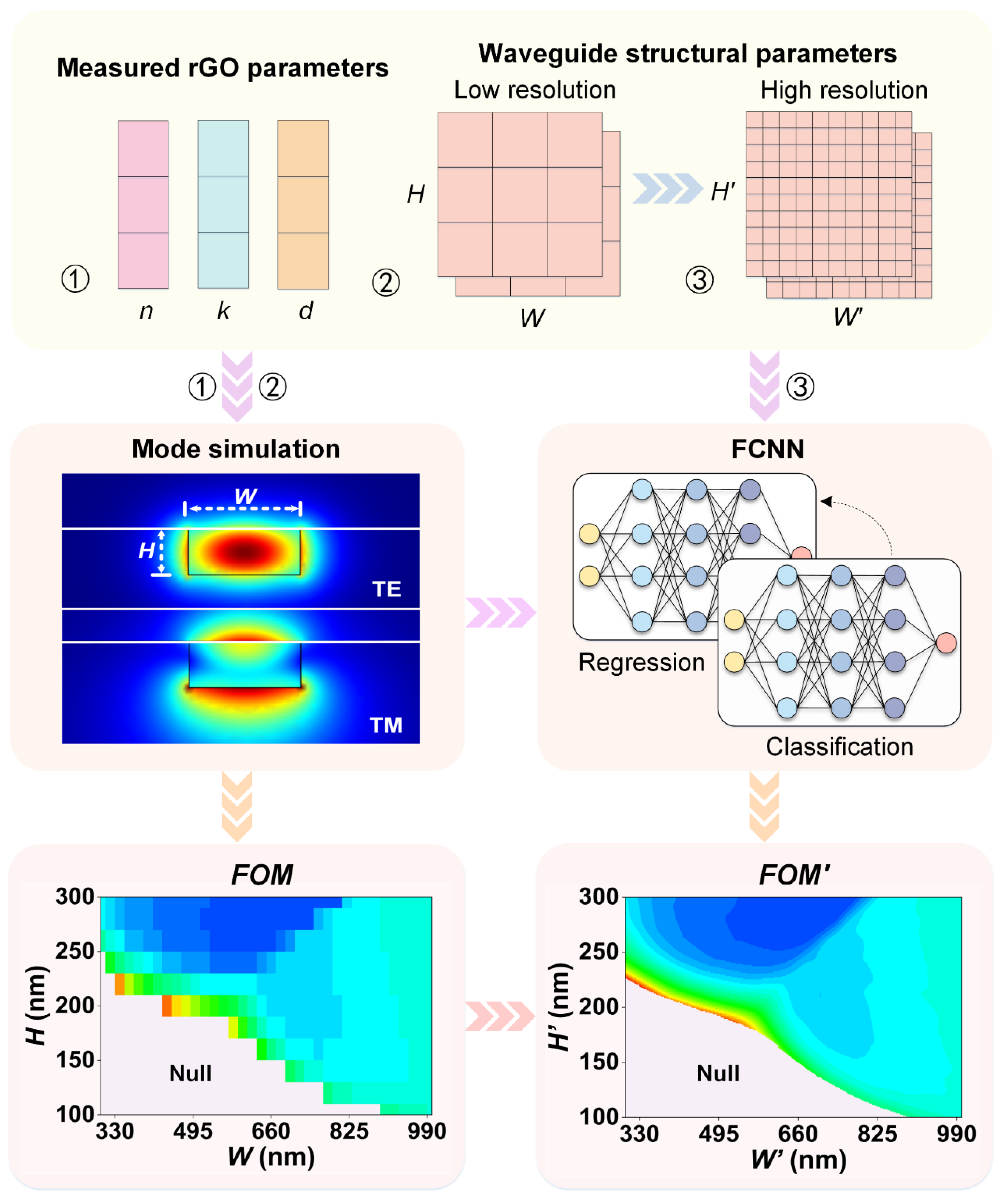
Figure 3.
Schematic illustration of the FCNN framework, which comprises two subnetworks FCNN-1 and FCNN-2 for identifying mode convergence and predicting polarizer FOM’s, respectively. Inset in the middle panel illustrates the architecture of either subnetwork, consisting of an input layer (L = 1), multiple hidden layers (L = 2, 3, …, m-1), and an output layer (L = m).
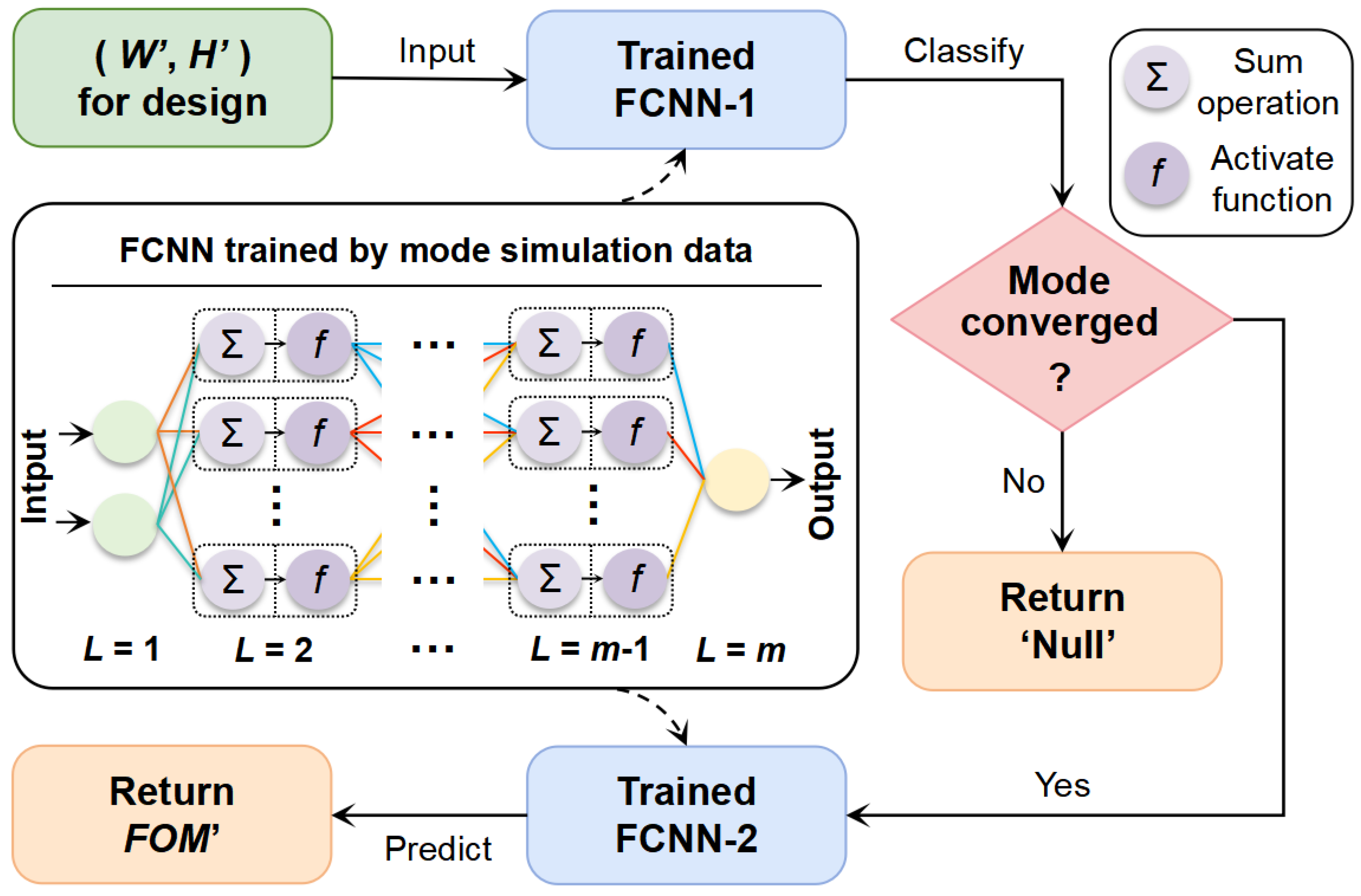
Figure 4.
a, c, e, FOM of rGO integrated waveguide polarizer versus low-resolution (W, H) with Δ = 80 nm, 40 nm, and 20 nm, respectively, where Δ is the step size between adjacent waveguide parameters within ranges of W ∈ [300, 1000] nm and H ∈ [100, 300] nm. The FOM values were calculated based on mode simulations and the ‘Null’ regions denote the cases of non-converged TE or TM modes in the simulations. b, d, f, FOM’ versus high-resolution (W’, H’) with Δ’ = 1 nm. The FOM’ values were predicted using FCNN-2, which was trained with the data in a, c, e, respectively. Regions labeled ‘Null’ correspond to non-converged TE or TM modes, as identified by FCNN-1.
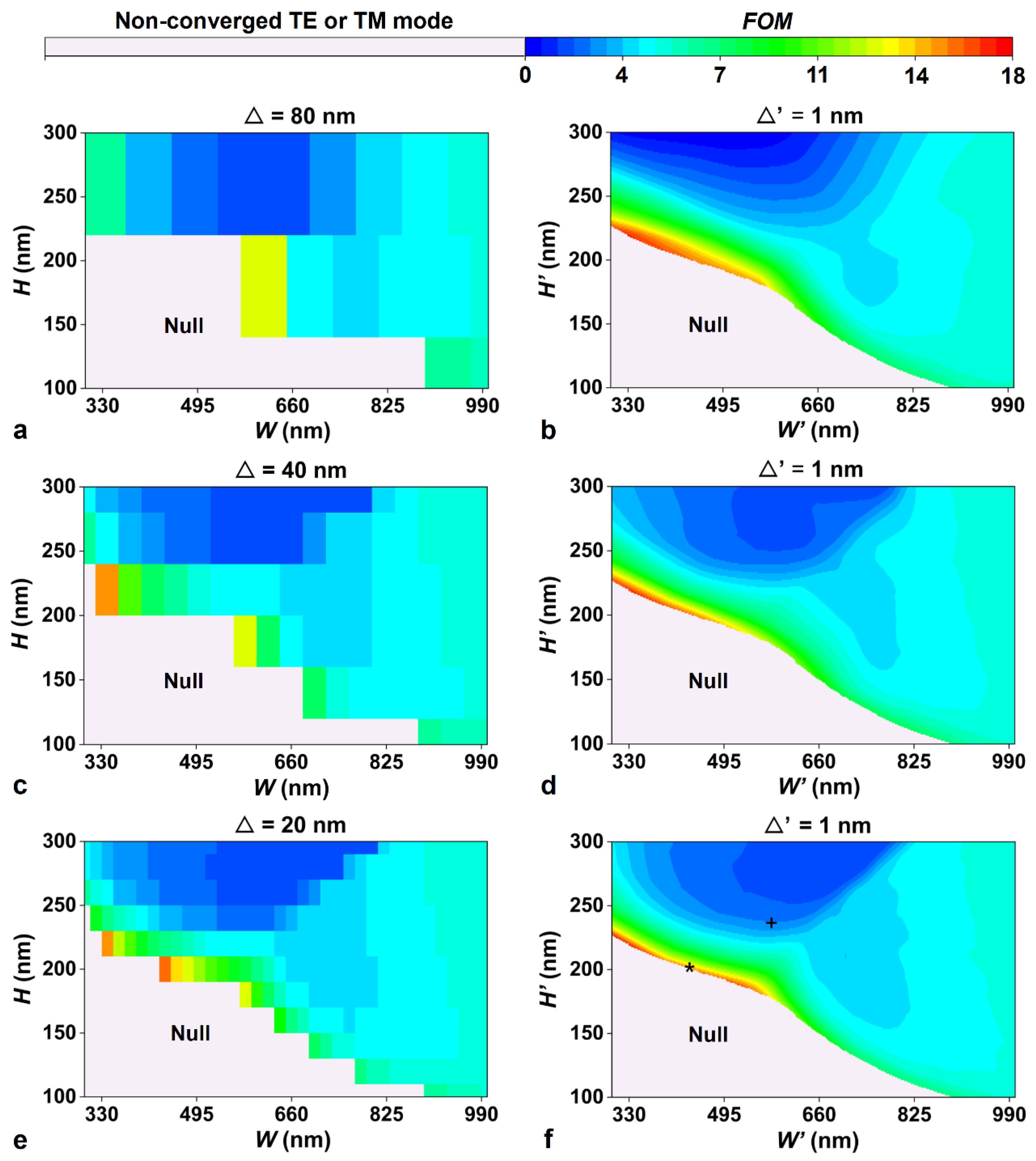
Figure 5.
TE and TM mode profiles corresponding to a high- and a low-FOM’ point in Figure 4f, marked by ‘*’ and ‘+’, respectively.
Figure 5.
TE and TM mode profiles corresponding to a high- and a low-FOM’ point in Figure 4f, marked by ‘*’ and ‘+’, respectively.
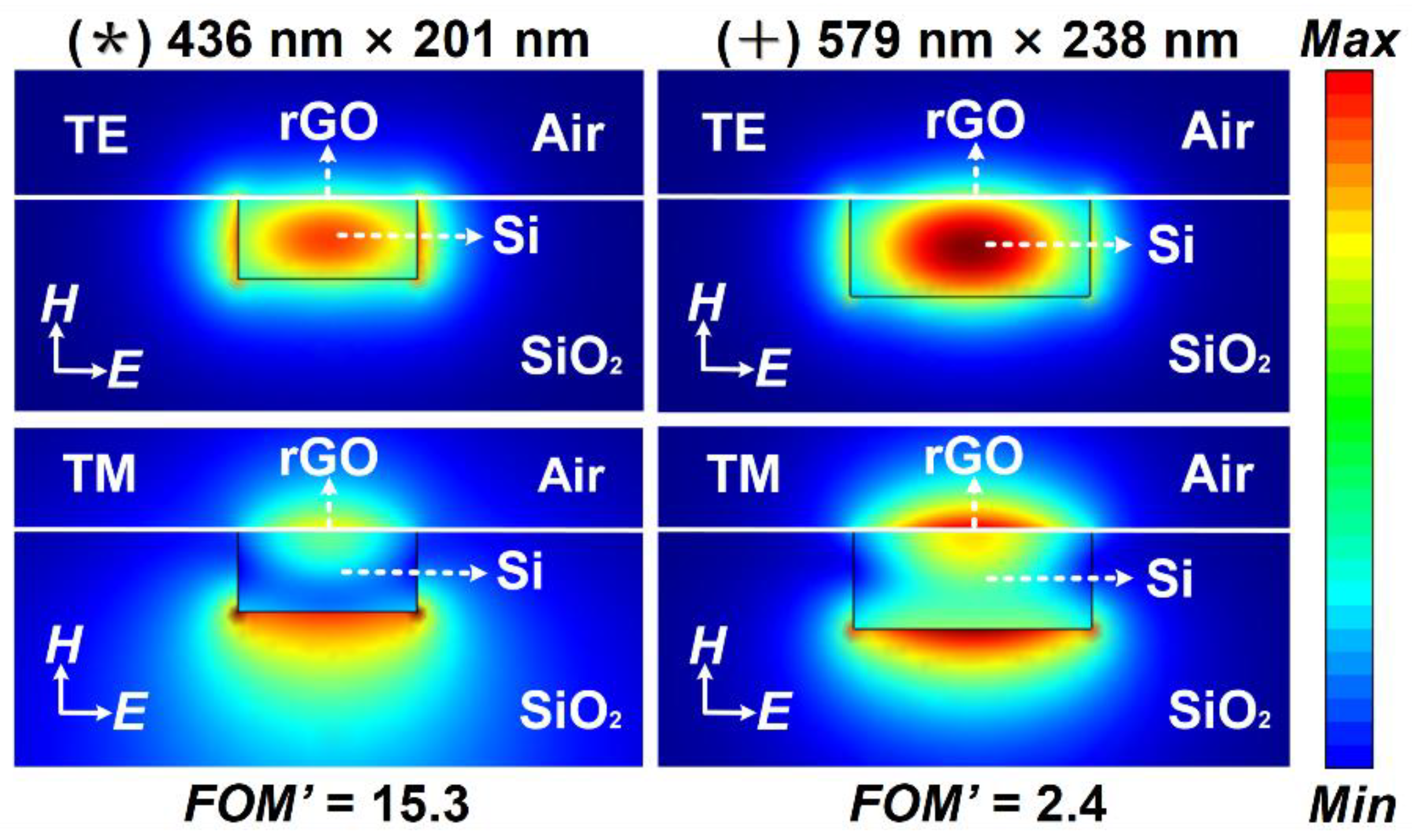
Figure 6.
a-i, FOM’ versus high-resolution (W’, H’) with Δ’ = 1 nm. The FOM’ values were predicted using FCNN-2, which was trained using the datasets No. 1 – No. 9 listed in Table 1, respectively. The ‘Null’ regions denote the cases of non-converged TE or TM modes, which were predicted using FCNN-1.

Figure 7.
Accuracy of FCNN-1 and average deviation (AD) of FCNN-2 for different training datasets (No. 1 – No. 9). The numbers of the (W, H) sets for each training dataset is also shown for comparison. The FCNN-1 for mode convergence identification and FCNN-2 for FOM’ prediction were trained on the datasets listed in Table 1, and tested on the dataset with Δ’ = 1 nm.
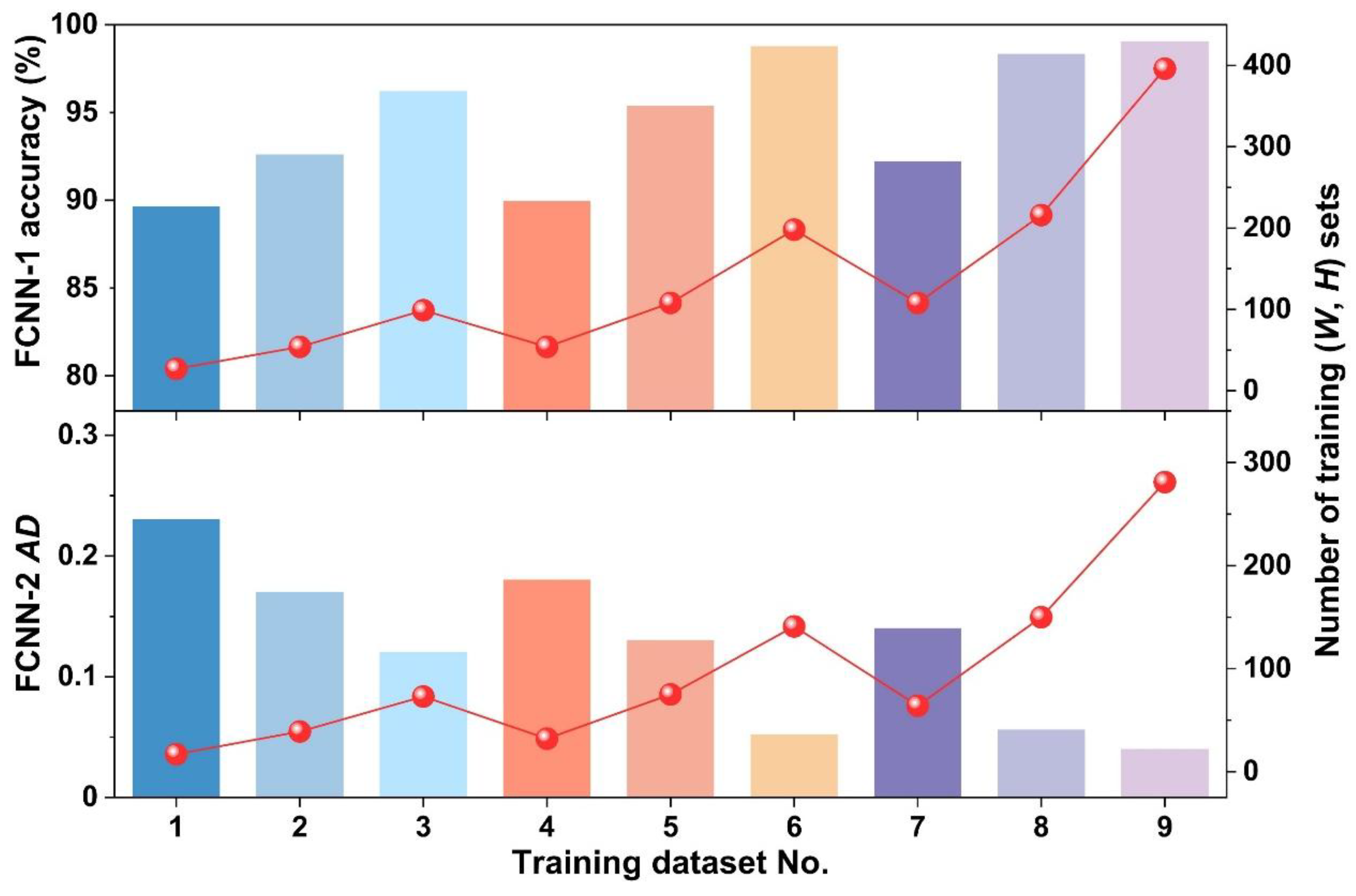

Table 1.
Various training datasets (W, H) for the FCNN-based framework.
| Dataset No. | ΔH (nm)a | ΔW (nm)a | Number of training sets for FCNN-1 | Number of training sets for FCNN-2 |
|---|---|---|---|---|
| 1 | 80 | 80 | 27 | 17 |
| 2 | 40 | 80 | 54 | 39 |
| 3 | 20 | 80 | 99 | 73 |
| 4 | 80 | 40 | 54 | 32 |
| 5 | 40 | 40 | 108 | 75 |
| 6 | 20 | 40 | 198 | 141 |
| 7 | 80 | 20 | 108 | 64 |
| 8 | 40 | 20 | 216 | 150 |
| 9 | 20 | 20 | 396 | 281 |
aΔW and ΔH are the step sizes used to uniformly sample W ∈ [300, 1000] nm and H ∈ [100, 300] nm, respectively, for establishing the training dataset (W, H).
Disclaimer/Publisher’s Note: The statements, opinions and data contained in all publications are solely those of the individual author(s) and contributor(s) and not of MDPI and/or the editor(s). MDPI and/or the editor(s) disclaim responsibility for any injury to people or property resulting from any ideas, methods, instructions or products referred to in the content. |
© 2025 by the authors. Licensee MDPI, Basel, Switzerland. This article is an open access article distributed under the terms and conditions of the Creative Commons Attribution (CC BY) license (http://creativecommons.org/licenses/by/4.0/).
Copyright: This open access article is published under a Creative Commons CC BY 4.0 license, which permit the free download, distribution, and reuse, provided that the author and preprint are cited in any reuse.


