Submitted:
18 September 2025
Posted:
18 September 2025
You are already at the latest version
Abstract
On-chip integration of highly anisotropic two-dimensional (2D) materials offers new opportunities for realizing high-performance polarization-selective devices. Obtaining optimized designs for such devices requires extensively sweeping large parameter spaces, which in conventional approaches relies on massive mode simulations that demand considerable computational resources. Here, we address this limitation by developing a machine learning model based on fully connected neural networks (FCNNs). Trained by using mode simulation results for low-resolution structural parameters, the FCNN model can accurately predict polarizer figures of merits (FOMs) for high-resolution parameters and rapidly map the global variation trend across the entire parameter space. We test the performance of the FCNN model using two types of polarizers with 2D graphene oxide (GO) and molybdenum disulfide (MoS2). Results show that, compared to conventional mode simulation approach, our approach can not only reduce the overall computing time by about 4 orders of magnitude, but also achieve highly accurate FOM predictions with an average deviation of less than 0.04. In addition, the measured FOM values for the fabricated devices show good agreement with the predicted ones, with discrepancies remaining below 0.2. These results validate artificial intelligence (AI) as an effective approach for designing and optimizing 2D-material-based optical polarizers with high efficiency.
Keywords:
machine learning
; 2D materials
; optical polarizers
; fully connected neural network
Introduction
The rapid advancement in artificial intelligence (AI) technology is revolutionizing the modeling and engineering of optical devices [1,2,3,4]. Compared to traditional simulation methods that rely on iterative Maxwell equations solving, AI offers a substantial improvement in computing efficiency by constructing neural networks that map structural parameters to optical responses, thereby directly capturing the underlying relationships [5,6,7,8]. This transformative approach is broadly applicable, with particular strength in addressing complex design challenges and optimizing sophisticated devices [1,2,9,10,11]. To date, the use of AI in optical device design has yielded substantial success in developing a variety of functional devices such as metasurfaces [8,12,13,14,15], nonlinear optical devices [16,17], electro-optic modulators [18], photodetectors [19,20,21], and quantum optical devices [22,23,24].
Optical polarizers are essential building blocks for selecting and controlling light polarization states in optical systems [25,26,27,28]. Recently, two-dimensional (2D) materials with strong anisotropic light absorption and broadband response have been utilized to implement optical polarizers, offering high device performance and novel features beyond what traditional bulk materials can achieve [25,26,29,30,31]. The performance of 2D-material-based optical polarizers is highly dependent on their device structural parameters [25,30,32,33]. Optimizing the design for these devices typically requires extensive sweeps across large parameter spaces. Conventional methods, which rely on comprehensive simulations via mode simulation software, are computationally demanding, particularly given that accurate mode simulations for devices with 2D materials require extremely fine meshing [34,35,36].
In this work, we develop a machine learning model based on fully connected neural networks (FCNNs) for the design and optimization of 2D-material-based optical polarizers. Trained on mode simulation results for low-resolution structural parameters, the FCNN model can accurately predict polarizer figures of merit (FOM) for high-resolution parameters and rapidly map the global FOM variation trend by sweeping the full parameter space. Two types of optical polarizers with 2D graphene oxide (GO) and molybdenum disulfide (MoS2) films are employed to test the performance of the FCNN model. Results show that our machine learning method can finish sweeping the full parameter space in 25‒35 s, in contrast to several months as required for mode simulations, and provides accurate FOM predictions with an average deviation (AD) of less than 0.04 relative to mode simulations. In addition, the measured FOM values for the fabricated polarizers agree well with those predicted by the FCNN model, with discrepancies below 0.2. These results confirm the effectiveness of AI as an efficient tool for the design and optimization of 2D-material-based optical polarizers.
Results and Discussion
Figure 1a shows the schematic of a 2D-material-based integrated waveguide polarizer, where a silicon (Si) photonic waveguide is coated with an atomically thin 2D material film, such as GO or MoS2. The right panel of Figure 1a depicts a schematic cross section of the hybrid waveguide, where W and H represent the width and height of the Si waveguide, respectively, and n, k, and d represent the refractive index, extinction coefficient, and thickness of the 2D material film, respectively. These structural parameters are critical for designing the polarizer and optimizing its performance.
Recent studies have revealed that 2D materials such as graphene [26,29,31,37,38], GO [30,32,33,39,40], transition metal dichalcogenides (TMDCs) [41,42,43,44,45], and MXenes [46,47] exhibit strong anisotropy in their light absorption, with light propagating in the in-plane direction showing significantly stronger absorption than that in the out-of-plane direction. Due to the interaction between the evanescent field from Si waveguide and the 2D material film with strong anisotropy in its light absorption, the hybrid waveguide in Figure 1a exhibits significantly stronger light absorption for transverse electric (TE, in-plane) polarization compared to transverse magnetic (TM, out-of-plane) polarization. This enables it to function as an effective TM-pass optical polarizer. In addition, 2D materials can exhibit strong anisotropy in their light absorption over a broad spectral range spanning from visible to infrared wavelengths [25]. This wide bandwidth provides a significant advantage for 2D-material-based integrated waveguide polarizers over conventional bulk Si photonic polarizers, which typically have limited operating bandwidths of less than 100 nm [26,29]. In the following discussion, we use 2D GO and MoS2 (a typical TMDC) films on a Si photonic platform as examples to demonstrate the effectiveness of our FCNN-based model. This choice is motivated by Si’s dominance in integrated photonic devices and our extensive prior research on these 2D material [30,42,48,49,50]. However, the operation principle is not limited to these 2D materials or Si platform and can be readily extended to other 2D materials (e.g., graphene and MXene) and integrated platforms (e.g., silicon nitride [51] and lithium niobate [52]).
Figure 1b illustrates the process flow for using a machine learning approach to predict polarizer figures of merit (FOM’) for high-resolution structural parameters (W’, H’) based on mode simulations with low-resolution parameters (W, H). It mainly includes three steps.
First, the 2D material parameters (n, k, d) are experimentally measured, which will be used for mode simulations in the next step. For instance, the 2D material film thickness can be characterized by using atomic force microscopy (AFM) [48]. The TE- and TM-polarized refractive indices (nTE, nTM) and extinction coefficients (kTE, kTM) of the 2D material film can be obtained by fitting the transmission spectra of 2D-material-coated microring resonators (MRRs) [53,54] based on the scattering matrix method [55,56].
Second, by using the measured 2D material parameters, mode simulations are performed for the hybrid waveguides with low-resolution (W, H) sets. For small values of W or H, the corresponding TE or TM modes may fail to converge, indicating that these dimensions meet the mode cut-off condition and the modes cannot physically exist. In such cases, the corresponding (W, H) is recorded as ‘Null’. When both TE and TM modes are converged, the power propagation losses (dB/cm) of the hybrid waveguide can be calculated by [53,54]
(1)
(2)
where kTE, eff and kTM, eff are the imaginary parts of the effective refractive indices for the TE and TM modes, respectively, L = 1 cm is the waveguide length, and λ is the light wavelength. Based on Eqs. (1) and (2), the polarizer figure of merit (FOM) can be further calculated by [30]
(3)
where PDL is the power dependent loss defined as the difference between the TE- and TM- polarized insertion losses, and it has been widely employed to quantify the polarization selectivity of optical polarizers [25,32,33]. EIL is the minimum excess insertion loss induced by the 2D film, which equals to the excess insertion loss for TM polarization. In 2D-material-based optical polarizers, the 2D material films not only provide high polarization selectivity but also introduce excess insertion loss. Therefore, the FOM defined in Eq. (3), which quantifies the trade-off between these two factors, is commonly used to assess the performance of 2D-material-based optical polarizers [25,29,30].
Finally, the recorded ‘Null’ for (W, H) corresponding to non-converged modes and the calculated FOM values for (W, H) corresponding to converged modes are used as the training dataset for the FCNN model. Once trained, the FCNN model can not only determine whether the TE or TM modes converge for a much larger test dataset containing high-resolution (W’, H’), but also predict the corresponding polarizer figure of merits FOM’s for the converged modes. The detailed framework of the FCNN model will be introduced in Figure 2. For clarity in comparison, in our following discussion the parameters of the training and test datasets are labeled in the same manner but with slight difference. For example, FOM, W, and H refer to the parameters for the training dataset, whereas FOM’, W’, and H’ correspond to those for the test dataset.
In order to optimize device structural parameters and achieve the maximum polarizer FOM, conventional approaches rely on commercial mode simulation software (such as COMSOL Multiphysics and Lumerical FDTD) to carry out exhaustive parameter sweeps over all sets of (W, H). For instance, scanning W ∈ [300, 1000] nm and H ∈ [100, 300] nm at 1-nm resolution would require simulations for over 140,000 sets of (W, H), with each simulation typically taking 5‒7 minutes. As a result, the computing time and cost become extremely high, particularly given the fact that the 2D material films (with thicknesses typically on the order of 1 nm) require ultra-fine mesh resolution to ensure accurate mode simulations.
In contrast, our approach uses machine learning to extract and model the relationships between structural parameters and modal behavior from a small number of (W, H) sets, allowing for rapid prediction of arbitrary high-resolution (W’, H’). In addition, performing an exhaustive sweep over all high-resolution (W’, H’) using our method adds minimal extra time compared to predicting a single set. For example, predicting the FOM’ for one set with converged mode takes 40‒80 ms, while sweeping over 140,000 sets of (W’, H’) requires only 25‒35 seconds, with each additional set contributing less than 1 ms to the total computing time. Except for saving substantial computing time and cost, our method also delivers high prediction accuracy. For example, using 396 sets of (W, H) as the training dataset, our method can achieve a high accuracy of ~99.0% in predicting mode convergence and a low average deviation (AD) of 0.018 when predicting the FOM’ for over 140,000 sets of (W’, H’).
Figure 2a illustrates the framework of the FCNN model designed for first identifying converged modes and then predicting the corresponding polarizer FOM’ for them. The trained FCNN model, which takes the high-resolution test dataset (W’, H’) as input, is composed of two subnetworks. The first one (FCNN-1) determines whether a mode is converged or not, and the second one (FCNN-2) predicts the polarizer FOM’ for the converged modes. Only the (W’, H’) corresponding to converged modes are sent to FCNN-2, which outputs the predicted FOM’ values. Both FCNN-1 and FCNN-2 have a similar architecture consisting of an input layer, multiple hidden layers, and an output layer, as illustrated in the inset of Figure 2a. Each layer contains a number of neurons, and every neuron is fully connected to all neurons in the following layer through weighted links. This architecture is typical for FCNNs, and similar to that in Refs [57,58]. Figure 2b illustrates the operation flow for a single neuron in FCNN-1, as marked by the dashed box in Figure 2a. The neuron takes a weighted sum of the outputs from all neurons in the previous layer, incorporates a bias, and outputs the result after applying a nonlinear activation function.
Before using the FCNN model in Figure 2a to identify converged modes and predict their corresponding polarizer FOM’ for high-resolution (W’, H’) sets, we trained it with the low-resolution training dataset (W, H). We started with training of FCNN-1 for mode convergence identification. Training dataset consisting of (W, H, C) pairs was constructed, with C encoded as 1 for converged and 0 for non-converged modes. This dataset was then normalized and passed forward to the input layer, generating the input vector h1 = (Wnorm, Hnorm). For a given layer p, the output of the j-th neuron is calculated by [59,60,61]
= (4)
where q is the total number of neurons in the layer p-1, is the output of the i-th neuron in the layer p-1, is the connection weight from the i-th neuron in the (p-1)-th layer to the j-th neuron in the p-th layer, is the bias of the j-th neuron in the current layer, and f is the activation function. The activation function f (x) is ReLU [62] throughout the network, except in the output layer where Sigmoid is applied, yielding the final output y ∈ [0, 1]. When y > 0.5, the input (W, H) is classified as a converged mode, if not, it is classified as non-converged. During the training, FCNN-1 evaluated its results against the ground-truth labels using the binary cross-entropy (BCE) loss and accuracy [7,63]. The gradients backpropagated to iteratively update the weights w and biases b across all layers, thereby enabling the network to learn the input-output mapping.
Following the training of FCNN-1, we trained FCNN-2 to perform polarizer FOM’ prediction. Mode-converged (W, H, FOM) sets were constructed as the training dataset and fed into FCNN-2. Similarly, FCNN-2 employs forward (Eq. (4)) and backpropagation, sharing a comparable fully connected architecture with FCNN-1. The key differences lie in their learning objectives and output designs. FCNN-1 performs binary convergence identification using a Sigmoid activation, with its performance evaluated by classification metrics such as BCE loss and accuracy. In contrast, FCNN-2 predicts continuous FOM values using a ReLU output activation, and its performance is assessed by regression metrics such as root mean square error (RMSE) and R2-score [7,63,64].
Figure 2c shows BCE loss and accuracy versus epoch for the training and validation datasets during the training of FCNN-1. We employed the Adam optimizer [65] with a learning rate of 1×10⁻⁴, a batch size of 128, and an early stopping criterion of 50 epochs. During the training process, the BCE loss decreased, whereas the accuracy increased. Until the metrics reached stable states after ~320 epochs, the model converged with a BCE loss of ~3.0×10⁻³ and an accuracy of ~99.9% for the training dataset, as well as a BCE loss of ~3.0×10⁻³ and an accuracy of ~99.8% for the validation dataset. These indicate that the model successfully converged to achieve an optimal level of identification performance.
Figure 2d shows RMSE and R2-score versus epoch for both training and validation datasets during the training of FCNN-2. The model was also trained using the Adam optimizer [65] with the same learning rate and early stopping criterion but a different batch size of 16. This is mainly due to the smaller size of the FCNN-2 dataset, where using a reduced batch size can effectively regularize the model against overfitting. As training progressed, a decrease in the RMSE was accompanied by an increase in the R2-score. After ~1300 epochs, the metrics stabilized, with the training dataset reaching an RMSE of ~2.5×10⁻² and an R2-score of ~0.999. On the other hand, the validation dataset achieved a BCE loss of ~4.6×10⁻² and an R2-score of ~0.997. These results confirm that FCNN-2 also converged into a stable state with robust predictive performance.
Based on the FCNN framework in Figure 2, we trained models for optimizing the FOM for GO-coated Si waveguide polarizers across varying waveguide width W and height H. For comparison, we selected training datasets containing different numbers of (W, H) sets, which correspond to different step sizes (i.e., Δ = 80 nm, 40 nm, and 20 nm) between adjacent parameters within the ranges of W ∈ [300, 1000] nm and H ∈ [100, 300] nm. A smaller step size Δ results in a larger number of (W, H) sets in the training dataset. For example, for mode-convergence identification, the dataset with Δ = 20 nm contains 396 sets, whereas the dataset with Δ = 80 nm only has 27 sets. The ranges of W and H were chosen to roughly span the convergence boundaries of the fundamental TE and TM modes for single-mode Si waveguides operating near 1550 nm. In addition, a high-resolution test dataset, generated with Δ’ = 1 nm within the same ranges of W’ ∈ [300, 1000] nm and H’ ∈ [100, 300] nm, was used to evaluate the trained models for mode-convergence identification and polarizer FOM’ prediction.
Figure 3a shows the FOM of GO-Si waveguide polarizer versus low-resolution (W, H) with a step size of Δ = 80 nm. The FOM values were calculated based on mode simulations using commercial software (COMSOL Multiphysics), and the ‘Null’ region corresponds to the (W, H) with non-converged TE or TM modes in the simulations. In our mode simulations, the GO film parameters (n, k, d) were obtained from our experimental measurements reported in Refs. [30,32]. For Δ = 80 nm, the (W, H) parameter space contains only 27 sets. As a result, Figure 3a appears as large, discretized patches, reflecting the limited resolution of the training dataset.
Figure 3b shows FOM’ versus high-resolution (W’, H’) with Δ’ = 1 nm, which was generated by the FCNN model in Figure 2a, trained using the low-resolution dataset in Figure 3a. The ‘Null’ region indicates cases of non-converged TE or TM modes identified by FCNN-1, whereas the FOM’ values in the convergent region were predicted by FCNN-2. Compared with Figure 3a, the results in Figure 3b exhibit much higher resolution, where the convergence boundaries and the trend of FOM’ variation remain consistent with the low-resolution results obtained from mode simulations. This demonstrates that the trained FCNN model can effectively predict high-resolution FOM’ by capturing how the variations in waveguide structural parameters influence mode convergence and FOM. We also note that the change of FOM’ with either W’ or H’ is non-monotonic, mainly resulting from non-monotonic changes in the mode overlap with the GO film. This complex dependence cannot be accurately modelled by simple interpolation or polynomial fitting, highlighting the challenges in optimizing the performance of such devices. In contrast, our machine learning approach can efficiently capture complex dependencies from a low-resolution dataset, providing a powerful tool for optimizing device structural parameters to achieve maximum FOM’.
Figure 3c,e show the FOM of GO-Si waveguide polarizer versus (W, H) with step sizes of Δ = 40 nm and 20 nm, respectively. Figure 3d,f show the corresponding FOM’ versus high-resolution (W’, H’) with Δ’ = 1 nm. For Δ = 40 nm and 20 nm, the training datasets contain 108 and 396 sets of (W, H), respectively. Compared with Figure 3a, these larger datasets provide more detailed mode simulation results for training our FCNN model. Similar to Figure 3b, the higher-resolution results in Figure 3d and 3f also capture the variation trends of the convergence boundaries and FOM obtained from mode simulations, further demonstrating that the FCNN model can effectively perform predictions based on low-resolution datasets.
Although the results in Figure 3b,d,f display the same resolution for (W’, H’), they actually have different prediction accuracies resulting from different sizes of their training datasets. To quantitatively analyze the prediction accuracy, we plot the accuracy of FCNN-1 and the average deviation (AD) of FCNN-2 for various Δ in Figure 3g. The accuracy of FCNN-1 is defined as the proportion of correctly classified cases, whereas the AD of FCNN-2 represents the mean absolute deviation between the values of predicted FOM’ and simulated FOM. As Δ decreases, the training dataset becomes larger, leading to increased accuracy of FCNN-1 and decreased AD of FCNN-2. This indicates that a larger training dataset allows the FCNN model to better capture the underlying relationships and thus improve prediction accuracy. At Δ = 20 nm, a maximum FCNN-1 accuracy of ~99.0% and the minimum FCNN-2 AD of ~0.018 are achieved. When Δ decreases from 40 nm to 20 nm, the variations in these two parameters become more significant than those observed when Δ decreases from 80 nm to 40 nm. This reflects the fact that the variation in prediction accuracy with the size of training dataset does not follow a linear trend. This is not surprising, as enlarging the training dataset not only increases the number of training (W, H) sets but also reveals finer variations in the (W, H) – FOM mapping that are not captured by smaller datasets.
Figure 3h shows the TE and TM mode profiles corresponding to a high- and a low-FOM’ point in Figure 3f marked by ‘*’ and ‘+’, respectively. The FOM’ values of these two points are ~5.16 and ~0.25, and the corresponding waveguide structural parameters (W’, H’) are (436 nm, 201 nm) and (579 nm, 238 nm), respectively. The huge difference between the high and low FOM’ values highlights the significance of optimizing waveguide structural parameters in the design of 2D-material-based optical polarizers. In addition, FOM values of ~5.13 and ~0.25 were obtained from mode simulations using the same waveguide structural parameters, closely matching the FOM’ values predicted by our FCNN model and reflecting the accuracy of our machine learning approach. We also note that the highest FOM’ values in Figure 3f are achieved near the mode convergence boundary, for example, the FOM’ value at (439 nm, 200 nm) is ~5.28. Although selecting (W, H) exactly at the convergence boundary can maximize the polarizer FOM, this comes at the expense of a limited operation bandwidth. For practical devices, the trade-off between an increased polarizer FOM and a decreased operation bandwidth should be balanced. A practical solution is to choose (W, H) slightly offset from the convergence boundary, which can provide a relatively high FOM together with a minor decrease in the operation bandwidth. These results further reflect the complexity in optimizing the performance of 2D-material-based optical polarizers.
In Figure 3, we compare the performance of our FCNN model using training datasets of different sizes (i.e., Δ = 80, 40, and 20 nm) while keeping a fixed test dataset size of Δ’ = 1 nm. In Figure 4, we further compare the performance of our FCNN model for test datasets of different sizes (i.e., Δ’ = 10, 5, 2, and 1 nm) while keeping the size of training dataset fixed at Δ = 20 nm. Here, we choose Δ = 20 nm for the training dataset because it provides the best prediction accuracy in Figure 3.
As shown in Figure 4a, the training dataset is generated with a step size of Δ = 20 nm and includes the FOM values of GO-coated Si waveguide polarizers for 396 sets of (W, H). Similar to Figure 3a, the FOM values were calculated based on mode simulations, and the ‘Null’ region corresponds to the (W, H) with non-converged TE or TM modes. Figure 4b‒e show FOM’ versus higher-resolution (W’, H’) with Δ’ = 10, 5, 2, and 1 nm, respectively, which were obtained by training the FCNN model using the low-resolution dataset in Figure 4a. As Δ’ decreases from 10 nm to 1 nm, the number of (W’, H’) sets in the test dataset increases from 1491 to 140,901, resulting in more refined convergence boundaries and more detailed FOM’ characteristics.
In Figure 4f, we compare the accuracy of FCNN-1 and the AD of FCNN-2 for various Δ’ in Figure 4b‒e. A decrease in Δ’ (i.e., a larger test dataset) results in decreased accuracy of FCNN-1 and increased AD of FCNN-2, showing a trend opposite to that observed in Figure 3g. This indicates that the FCNN model achieves lower prediction accuracy when applied to finer resolutions of the waveguide structural parameters. When Δ’ decreases from 10 nm to 1 nm, the accuracy of FCNN-1 decreases from ~99.8% to ~99.0%, whereas the AD of FCNN-2 increases from ~0.01 to ~0.018, showing only minor degradation in the prediction accuracy. This confirms the accuracy of our FCNN model when applied to test datasets much larger than the training dataset.
To demonstrate the universality of our approach, the FCNN model in Figure 2a was also applied to optimizing the FOM of MoS2-Si waveguide polarizers. Following the same procedure for optimizing the GO-Si polarizers, the model was trained using mode simulation results for low-resolution (W, H) sets, and its prediction accuracy is evaluated on a larger test dataset consisting of high-resolution (W’, H’) sets.
Figure 5a shows the FOM of MoS2-Si waveguide polarizer versus low-resolution (W, H) with a step size of Δ = 20 nm. Similar to Figures 3a and 4a, the FOM values and the ‘Null’ region corresponding to non-converged TE or TM modes were obtained based on mode simulations. In our mode simulations, the MoS2 film parameters (n, k, d) were obtained from our experimental measurements reported in Ref. [50]. In Figure 5b, higher-resolution FOM’ values were predicted at a step size of Δ’ = 1 nm. Both the FOM’ values and ‘Null’ region were predicted by the FCNN model trained by using the low-resolution dataset in Figure 5a. As can be seen, the higher-resolution predictions not only closely match the low-resolution results, but also reveal finer features of the convergence boundaries and FOM variation ‒ similar to those observed in Figure 4e.
Figure 5c shows the TE and TM mode profiles corresponding to a high- and a low-FOM’ point in Figure 5b marked by ‘*’ and ‘+’, respectively. The corresponding waveguide structural parameters (W’, H’) are (436 nm, 201 nm) and (579 nm, 238 nm), with FOM’ values of ~7.21 and ~0.71, respectively. Mode simulations show FOM values of ~7.23 and ~0.72 for the same structural parameters ‒ agreeing well with the predicted FOM’ values. This confirms that our FCNN model is also effective for optimizing MoS2–Si optical polarizers.
Figure 5d compares the accuracy of our FCNN model for predicting GO-Si and MoS2-Si polarizers. For mode convergence identification, since the influence of ultrathin 2D materials on mode convergence is negligible as compared to bulk Si waveguides, the prediction accuracy of FCNN-1 for the two types of polarizers is almost the same (which has already been shown in Figure 4f). Therefore, here we focus on comparing FOM’ prediction based on FCNN-2. As shown in Figure 5d, the AD of FCNN-2 for predicting MoS2-Si polarizers is ~0.033, which is slightly higher than ~0.018 obtained for GO-Si polarizers. Such difference can be attributed to a larger FOM value range of MoS2 polarizers (i.e., [0, 8]) as compared to that for GO polarizers (i.e., [0, 6]). When the target variable spans a wider range, the FCNN model needs to learn a more extensive input-output mapping. With a fixed training dataset size, certain subranges might receive insufficient coverage, thus leading to increased prediction deviations. Nevertheless, the two types of polarizers exhibit small AD values on the order of 10-2. This confirms the high accuracy of our machine learning approach when applied to different types of 2D-material-based optical polarizers.
To provide a comprehensive evaluation of our approach, we test our FCNN model under various conditions and compare the performance with respect to computing time and prediction accuracy. Figure 6a compares the single-point computing times of the mode simulation and machine learning methods. Results for ten test points are shown, each corresponding to a specific (W, H) for mode simulation or a (W’, H’) serving as input for the FCNN model. The computing times for the FCNN-based machine learning method are evaluated in two stages, one corresponds to predictions of mode convergence using only FCNN-1, and the other corresponds to predictions of FOM’ using both FCNN-1 and FCNN-2.
As can be seen, the mode simulation method requires ~300–400 s to finish computing for one point. This process includes three steps: (i) performing mode simulations with software, (ii) manually identifying fundamental TE or TM modes and verifying convergence, and (iii) calculating the FOM values based on the mode simulation results. In our case, mode simulations (using COMSOL Multiphysics) in the first step account for over 80% of the total computing time, which was performed on a standard personal computer equipped with an Intel(R) Core (TM) i7-7700K CPU running at 4.20 GHz and 32.0 GB of RAM. In contrast, the trained FCNN model completed mode convergence identification through FCNN-1 in only ~0.01–0.03 s, and the entire FOM’ prediction process involving both FCNN-1 and FCNN-2 required only ~0.04–0.08 s ‒ about 4 orders of magnitude faster than the mode simulation method. This remarkable acceleration results from replacing repeated numerical solving with a simple forward pass of the trained network, in which the input parameters are processed through a series of matrix multiplications and nonlinear activation functions to produce the output.
Figure 6b shows overall computing time of the FCNN model versus step size of Δ for (W, H) in the training dataset. The overall computing time refers to the total time required for all (W’, H’) in the test dataset with a step size of Δ’ = 1 nm. Similar to Figure 3, a larger Δ leads to a smaller size of the training dataset. As the step size Δ increases from 5 nm to 80 nm, the number of (W, H) sets decreases from 5781 to 27. Since the prediction of FCNN-1 for mode convergence identification mainly depends on the model architecture and the size of test dataset, the overall computing time for FCNN-1 remains largely unaffected by the size of the training dataset, staying nearly constant at ~5 s. On the basis of FCNN-1, FCNN-2 was employed to predict the FOM’ values for (W’, H’) corresponding to the converged modes. The overall computing times for both FCNN-1 and FCNN-2 remain in the range of ~25–35 s. Compared with FCNN-1, FCNN-2 dominates the overall computing time, accounting for ~80 %. The higher computing time of FCNN-2 arises from its need to perform more complex regression tasks for accurate prediction of FOM’ values (as compared to FCNN-1 that only carries out binary classification for mode convergence identification), as well as its larger network architecture (e.g., having 128 neurons per hidden layer compared with 64 in FCNN-1). We also note that the overall computing times for both FCNN-1 and FCNN-2 show no significant variation with the size of training dataset, mainly because the forward computing time of the FCNN model primarily depends on the complexity of the model architecture and the size of test dataset.
According to Figure 6a,b, the mode simulation method requires ~300–400 s to finish computing for a single point. Exhaustively sweeping all (W’, H’) in the test dataset with a step size of Δ’ = 1 nm results in an overall computing time on the order of ~107 s (i.e., over 100 days of continuous running), highlighting the extremely demanding computing time and cost. In contrast, our FCNN model offers substantial savings in computing time and cost, requiring less than 40 s to exhaustively sweep all (W’, H’) in a test dataset of the same size. This also highlights the advantage of our FCNN model in handling massive sets of device structural parameters for performance optimization.
In addition to computing time, prediction accuracy serves as another key metric for evaluating the performance of the FCNN model. Figure 6c illustrates accuracy of FCNN-1 versus Δ, where the step size of test dataset is fixed at Δ’ = 1 nm. Here we present additional results for different Δ values to extend the results in Figure 3g and provide a more detailed analysis of the influence of training dataset size on the prediction accuracy. The accuracy of FCNN-1 decreases as Δ increases. The decrease is gradual for Δ in the range of [2, 20], and becomes more significant for larger Δ values, indicating that prediction accuracy does not decrease linearly with increasing training dataset size. This is a combined result caused by multiple factors ‒ most notably reduced data diversity and inadequate representation of feature distributions ‒ which limit FCNN-1 to capture finer variations in the input-output mapping that are essential for achieving higher prediction accuracy. Although a larger training dataset improves the accuracy of FCNN-1, it also increases the computing time and cost required for constructing the training dataset. Therefore, a trade-off between them should be properly balanced for practical applications. In our case, the selection of Δ = 20 nm in Figure 4 and Figure 5 was also based on considerations of such trade-off.
Figure 6d shows the confusion matrix of FCNN-1 with a step size of Δ = 20 nm for the training dataset, which corresponds to the point in the dashed circle marked in Figure 6c. The confusion matrix can be used to evaluate the agreement between the truth and predicted labels for mode convergence identification, where ‘C’ denotes converged modes and ‘NC’ represents non-converged TE or TM modes. The values in the matrix represent the numbers of (W’, H’) sets for different cases, and their sum equals 140,901, which is the total number of (W’, H’) sets in the test dataset. In our test, we observed that 101,475 sets for converged modes and 38,058 sets for non-converged modes were correctly identified, and only 465 sets for non-converged modes and 903 sets for converged modes were misclassified as the opposite label. These results in an overall accuracy of FCNN-1 exceeding 99% and an error rate below 1%. This demonstrates that the high accuracy of FCNN-1 for mode convergence identification and its reliability in supporting subsequent prediction of FOM’ using FCNN-2.
In Figure 6e,f, we further evaluate the prediction accuracy of FCNN-2. Figure 6e shows the AD of FCNN-2 versus step size Δ of the training dataset. Here we show the results for both GO-Si and MoS2-Si polarizers with the same step size of Δ’ = 1 nm for the test dataset. Similar to Figure 6c, the prediction accuracy decreases with increasing Δ, and the variation of AD with Δ does not exhibit a linear relationship. In addition, FCNN-2 also involves a trade-off between improving prediction accuracy and controlling the cost for constructing the training dataset. In Figure 6e, a dramatic increase in the AD of FCNN-2 is observed only when Δ rises beyond 20 nm, which was another reason for selecting Δ = 20 nm in Figure 4 and Figure 5.
Figure 6f shows the comparison between FCNN-2 predictions and mode simulation results for the points in the dashed circle marked in Figure 6e. The step size of training dataset is Δ = 20 nm, and the step size of test dataset is Δ’ = 1 nm. Each dot represents one data point, and the black dashed line indicates the diagonal reference. As can be seen, the points for both GO and MoS2 polarizers cluster closely around the diagonal reference, indicating high prediction accuracy of FCNN-2. In addition, the MoS2 polarizers exhibit greater errors compared with GO polarizers, as explained in the discussion of Figure 5d. The inset of Figure 6f shows the corresponding prediction error distribution curves. Compared with the MoS2 polarizers, the GO polarizers exhibit a higher and narrower zero-centered error distribution, indicating better prediction accuracy and consistency.
To further validate the effectiveness of our FCNN model, we practically fabricate GO-Si and MoS2-Si waveguide polarizers. In our fabrication, we first fabricated uncoated Si waveguides on a silicon-on-insulator (SOI) wafer with a 220-nm-thick top Si layer and a 2-μm-thick silica layer. The waveguide patterns were defined using 248-nm deep ultraviolet photolithography, followed by inductively coupled plasma (ICP) etching that enabled waveguide formation. Next, a 1.5-μm-thick silica upper cladding layer was deposited on the SOI chip via plasma enhanced chemical vapor deposition (PECVD). Finally, windows of different lengths were opened on the upper cladding through the processes of photolithography and reactive ion etching (RIE) to enable the coating of 2D material films onto the Si waveguides. All the fabricated Si waveguides had the same length of ~3.0 mm, and the lengths of opened windows (i.e., the 2D film coating lengths) ranged between ~0.1 mm and ~2.2 mm.
After fabricating the uncoated Si waveguides, monolayer 2D material films were coated on them using different methods. For GO, we employed a solution-based approach that enabled transfer-free and layer-by-layer film coating. For MoS2, MoS2 films were synthesized by low-pressure chemical vapor deposition (LPCVD) and subsequently transferred onto the Si waveguides using polymer-assisted transfer process. Detailed fabrication processes for these are provided in Refs. [32,33,48]
Figure 7a,b show microscopic images of the fabricated GO-Si and MoS2 -Si waveguide polarizers. The transferred 2D material films exhibit good morphology and uniform coverage across the SOI chip surface, confirming the effectiveness and quality of the film coating. Figure 7c,d show Raman spectra of SOI chips before and after coating 2D GO and MoS2 film, respectively. The Raman spectra were characterized by using a ~514-nm excitation laser. The presence of characteristic peaks at ~1345 cm-1 and ~1590 cm-1 for the GO-coated chip, and at ~384 cm-1 and ~404 cm-1 for the MoS2-coated chip, provides evidence for successful on-chip integration of these 2D films.
Figure 7e,f compare the experimentally measured FOM values with FOM’ values predicted by the FCNN model. The data points for the experimental results depict the average of measurements on four devices with different 2D film coating lengths (i.e., 0.2 mm, 0.4 mm, 1.0 mm, 2.2 mm), and the error bars illustrate the variations among these devices. As can be seen, the predicted FOM’ values agree well with the experimental results, with minor discrepancies mainly arising from fabrication-induced variations in the device structural parameters (e.g., 2D film thicknesses). For both types of polarizers, the predicted and measured values differ by less than 0.2, with the minimum deviation reaching 0.01. These results highlight the high accuracy of our FCNN model in guiding practical device design. Since we only have SOI wafers with a 220-nm-thick top Si layer, we are unable to fabricate GO and MoS2 polarizers achieving higher FOM’ values in Figure 3 and Figure 5. As discussed in Figure 3h, the highest FOM’ values are usually achieved near the mode convergence boundary, where choosing (W, H) exactly at the boundary can maximize the polarizer FOM but limit the operation bandwidth. Therefore, the variation trend of FOM’, which provides valuable guidance for balancing the above trade-off, is more important than simply finding the highest FOM’ points. As discussed in Figure 3b, our machine learning method is particularly powerful in mapping the global variation trend of FOM’ by rapidly sweeping across all sets of device structural parameters. This highlights the strength of our approach in addressing the complex requirements of practical device design. These results are applicable to a wide range of linear and nonlinear integrated devices including microcombs Refs. [67,68,69,70,71,72,73,74,75,76,77,78,79,80,81,82,83,84,85,86,87,88,89,90,91,92,93,94,95,96,97,98,99,100,101,102,103,104,105,106,107,108,109,110,111,112,113,114,115,116,117,118,119,120,121,122,123,124,125,126,127,128,129,130,131,132,133,134,135,136,137,138,139,140,141,142,143,144] and graphene oxide based integrated chips, Refs. [145,146,147,148,149,150,151,152,153,154,155,156,157,158,159,160,161,162,163,164,165,166,167,168,169,170,171,172,173,174,175,176,177,178,179,180,181,182,183,184,185,186] quantum optical chips Refs. [187,188,189,190,191,192,193,194,195,196,197,198,199,200,201,202] and a range of other devices. Refs. [187,188,189,190,191,192,193,194,195,196,197,198,199,200,201,202,203,204,205,206,207,208,209,210,211,212]
Conclusions
In summary, an FCNN-based machine learning model is developed for design and optimization of 2D-material-based optical polarizers. Trained on mode simulation results for low-resolution structural parameters, the FCNN model can accurately predict the polarizer FOM values for high-resolution structural parameters and rapidly sweep the entire parameter space to map the global variation trend. The performance of the FCNN model is tested using two types of polarizers with 2D GO and MoS2 films. Results show that our machine learning method can reduce the overall computing time from several months as required for mode simulations to ~30 s, and achieve accurate FOM predictions with an average deviation of less than 0.04 relative to mode simulation results. In addition, the measured FOM values of fabric[67–144ated polarizers show excellent agreement with those predicted by the FCNN model, with the discrepancies remaining below 0.2. Our work opens new avenues for leveraging AI to facilitate the design and optimization of 2D-material-based optical polarizers.
Declaration of competing interest: The authors declare no competing interests.
References
- Ma, W.; Liu, Z.; Kudyshev, Z.A.; Boltasseva, A.; Cai, W.; Liu, Y. Deep learning for the design of photonic structures. Nature photonics 2021, 15, 77–90. [Google Scholar]
- Jiang, J.; Chen, M.; Fan, J. Deep neural networks for the evaluation and design of photonic devices. Nature Reviews Materials, 2020; /17. [Google Scholar]
- Molesky, S.; Lin, Z.; Piggott, A.Y.; Jin, W.; Vucković, J.; Rodriguez, A.W. Inverse design in nanophotonics. Nature Photonics 2018, 12, 659–670. [Google Scholar] [CrossRef]
- Yang, J.; Guidry, M.A.; Lukin, D.M.; Yang, K.; Vučković, J. Inverse-designed silicon carbide quantum and nonlinear photonics. Light: Science & Applications 2023, 12, 201. [Google Scholar] [CrossRef]
- Peurifoy, J.; Shen, Y.; Jing, L.; Yang, Y.; Cano-Renteria, F.; DeLacy, B.G.; Joannopoulos, J.D.; Tegmark, M.; Soljačić, M. Nanophotonic particle simulation and inverse design using artificial neural networks. Science Advances 2018, 4, eaar4206. [Google Scholar] [CrossRef] [PubMed]
- Xu, Y.; Zhang, X.; Fu, Y.; Liu, Y. Interfacing photonics with artificial intelligence: a new design strategy for photonic structures and devices based on artificial neural networks. Photonics Research 2021, 9. [Google Scholar] [CrossRef]
- Xu, X.; Tan, M.; Corcoran, B.; Wu, J.; Boes, A.; Nguyen, T.G.; Chu, S.T.; Little, B.E.; Hicks, D.G.; Morandotti, R.; Mitchell, A.; Moss, D.J. 11 tops photonic convolutional accelerator for optical neural networks. Nature 2021, 589, 44–51. [Google Scholar] [CrossRef] [PubMed]
- Malkiel, I.; Mrejen, M.; Nagler, A.; Arieli, U.; Wolf, L.; Suchowski, H. Plasmonic nanostructure design and characterization via deep learning. Light: Science & Applications 2018, 7, 60. [Google Scholar] [CrossRef]
- Estakhri, N.M.; Edwards, B.; Engheta, N. Inverse-designed metastructures that solve equations. Science 2019, 363, 1333–1338. [Google Scholar] [CrossRef]
- He, M.; Nolen, J.R.; Nordlander, J.; Cleri, A.; McIlwaine, N.S.; Tang, Y.; Lu, G.; Folland, T.G.; Landman, B.A.; Maria, J.-P. Deterministic inverse design of Tamm plasmon thermal emitters with multi-resonant control. Nature materials 2021, 20, 1663–1669. [Google Scholar] [CrossRef] [PubMed]
- Dory, C.; Vercruysse, D.; Yang, K.Y.; Sapra, N.V.; Rugar, A.E.; Sun, S.; Lukin, D.M.; Piggott, A.Y.; Zhang, J.L.; Radulaski, M.; Lagoudakis, K.G.; Su, L.; Vučković, J. Inverse-designed diamond photonics. Nature Communications 2019, 10, 3309. [Google Scholar] [CrossRef]
- Ueno, A.; Hu, J.; An, S. AI for optical metasurface. npj Nanophotonics 2024, 1, 36. [Google Scholar] [CrossRef]
- Zhu, R.; Qiu, T.; Wang, J.; Sui, S.; Hao, C.; Liu, T.; Li, Y.; Feng, M.; Zhang, A.; Qiu, C.-W.; Qu, S. Phase-to-pattern inverse design paradigm for fast realization of functional metasurfaces via transfer learning. Nature Communications 2021, 12, 2974. [Google Scholar] [CrossRef] [PubMed]
- Zhu, E.; Zong, Z.; Li, E.; Lu, Y.; Zhang, J.; Xie, H.; Li, Y.; Yin, W.-Y.; Wei, Z. Frequency transfer and inverse design for metasurface under multi-physics coupling by Euler latent dynamic and data-analytical regularizations. Nature Communications 2025, 16, 2251. [Google Scholar] [CrossRef] [PubMed]
- Liu, Z.; Zhu, D.; Rodrigues, S.P.; Lee, K.-T.; Cai, W. Generative model for the inverse design of metasurfaces. Nano Letters 2018, 18, 6570–6576. [Google Scholar] [CrossRef]
- Fan, Q.; Zhou, G.; Gui, T.; Lu, C.; Lau, A.P.T. Advancing theoretical understanding and practical performance of signal processing for nonlinear optical communications through machine learning. Nature Communications 2020, 11, 3694. [Google Scholar] [CrossRef]
- Genty, G.; Salmela, L.; Dudley, J.M.; Brunner, D.; Kokhanovskiy, A.; Kobtsev, S.; Turitsyn, S.K. Machine learning and applications in ultrafast photonics. Nature Photonics 2021, 15, 91–101. [Google Scholar] [CrossRef]
- de Paula, R.A.; Aldaya, I.; Sutili, T.; Figueiredo, R.C.; Pita, J.L.; Bustamante, Y.R.R. Design of a silicon Mach–Zehnder modulator via deep learning and evolutionary algorithms. Scientific Reports 2023, 13, 14662. [Google Scholar] [CrossRef]
- Choi, S.B.; Choi, J.S.; Shin, H.S.; Yoon, J.-W.; Kim, Y.; Kim, J.-W. Deep learning-developed multi-light source discrimination capability of stretchable capacitive photodetector. npj Flexible Electronics 2025, 9, 44. [Google Scholar] [CrossRef]
- Ayyubi, R.A.W.; Low, M.X.; Salimi, S.; Khorsandi, M.; Hossain, M.M.; Arooj, H.; Masood, S.; Zeb, M.H.; Mahmood, N.; Bao, Q.; Walia, S.; Shabbir, B. Machine learning-assisted high-throughput prediction and experimental validation of high-responsivity extreme ultraviolet detectors. Nature Communications 2025, 16, 6265. [Google Scholar] [CrossRef]
- Oh, S.; Kim, H.; Meyyappan, M.; Kim, K. Design and analysis of near-IR photodetector using machine learning approach. IEEE Sensors Journal 2024, 24, 25565–25572. [Google Scholar] [CrossRef]
- Kudyshev, Z.A.; Sychev, D.; Martin, Z.; Yesilyurt, O.; Bogdanov, S.I.; Xu, X.; Chen, P.-G.; Kildishev, A.V.; Boltasseva, A.; Shalaev, V.M. Machine learning assisted quantum super-resolution microscopy. Nature Communications 2023, 14, 4828. [Google Scholar] [CrossRef]
- Kudyshev, Z.A.; Shalaev, V.M.; Boltasseva, A. Machine learning for integrated quantum photonics. ACS Photonics 2021, 8, 34–46. [Google Scholar] [CrossRef]
- Torlai, G.; Mazzola, G.; Carrasquilla, J.; Troyer, M.; Melko, R.; Carleo, G. Neural-network quantum state tomography. Nature Physics 2018, 14, 447–450. [Google Scholar] [CrossRef]
- Zhang, Y.; Wu, J.; Linnan, J.; Jin, D.; Jia, B.; Hu, X.; Moss, D.; Gong, Q. Advanced optical polarizers based on 2D materials. npj Nanophotonics 2024, 1. [Google Scholar] [CrossRef]
- Bao, Q.; Zhang, H.; Wang, B.; Ni, Z.; Lim, C.H.Y.X.; Wang, Y.; Tang, D.Y.; Loh, K.P. Broadband graphene polarizer. Nature Photonics 2011, 5, 411–415. [Google Scholar] [CrossRef]
- He, C.; He, H.; Chang, J.; Chen, B.; Ma, H.; Booth, M.J. Polarisation optics for biomedical and clinical applications: a review. Light: Science & Applications 2021, 10, 194. [Google Scholar] [CrossRef] [PubMed]
- Dai, D.; Liu, L.; Gao, S.; Xu, D.X.; He, S. Polarization management for silicon photonic integrated circuits. Laser & Photonics Reviews 2013, 7, 303–328. [Google Scholar]
- Lin, H.; Song, Y.; Huang, Y.; Kita, D.; Deckoff-Jones, S.; Wang, K.; Li, L.; Li, J.; Zheng, H.; Luo, Z.; Wang, H.; Novak, S.; Yadav, A.; Huang, C.-C.; Shiue, R.-J.; Englund, D.; Gu, T.; Hewak, D.; Richardson, K.; Kong, J.; Hu, J. Chalcogenide glass-on-graphene photonics. Nature Photonics 2017, 11, 798–805. [Google Scholar] [CrossRef]
- Wu, J.; Yang, Y.; Qu, Y.; Xu, X.; Liang, Y.; Chu, S.T.; Little, B.E.; Morandotti, R.; Jia, B.; Moss, D.J. Graphene oxide waveguide and micro-ring resonator polarizers. Laser & Photonics Reviews 2019, 13. [Google Scholar]
- Kim, J.T.; Choi, H. Polarization control in graphene-based polymer waveguide polarizer. Laser & Photonics Reviews 2018, 12, 1800142. [Google Scholar]
- Hu, J.; Wu, J.; Jin, D.; Liu, W.; Zhang, Y.; Yang, Y.; Jia, L.; Wang, Y.; Huang, D.; Jia, B.; Moss, D.J. Integrated photonic polarizers with 2D reduced graphene oxide. Opto-Electronic Science 2025, 2025, 240032. [Google Scholar] [CrossRef]
- Jin, D.; Wu, J.; Hu, J.; Liu, W.; Zhang, Y.; Yang, Y.; Jia, L.; Huang, D.; Jia, B.; Moss, D.J. Silicon photonic waveguide and microring resonator polarizers incorporating 2D graphene oxide films. Applied Physics Letters 2024, 125. [Google Scholar] [CrossRef]
- Wiecha, P.R.; Arbouet, A.; Girard, C.; Muskens, O.L. Deep learning in nano-photonics: inverse design and beyond. Photonics Research 2021, 9, B182–B200. [Google Scholar] [CrossRef]
- Chen, W.-J.; Zhu, Q.-Y. FDTD algorithm for subcell model with cells containing layers of graphene thin sheets. IEICE Electronics Express 2024, 21, 20240449. [Google Scholar] [CrossRef]
- Chen, J.; Wang, J. Three-dimensional dispersive hybrid implicit–explicit finite-difference time-domain method for simulations of graphene. Computer Physics Communications 2016, 207, 211–216. [Google Scholar] [CrossRef]
- Kim, J.T.; Choi, C.-G. Graphene-based polymer waveguide polarizer. Optics Express 2012, 20, 3556–3562. [Google Scholar] [CrossRef] [PubMed]
- Pei, C.; Yang, L.; Wang, G.; Wang, Y.; Jiang, X.; Hao, Y.; Li, Y.; Yang, J. Broadband graphene/glass hybrid waveguide polarizer. IEEE Photonics Technology Letters 2015, 27, 927–930. [Google Scholar] [CrossRef]
- Chong, W.S.; Gan, S.X.; Lai, C.K.; Chong, W.Y.; Choi, D.; Madden, S.; Rue, R.M.D.L.; Ahmad, H. Configurable TE- and TM-pass graphene oxide-coated waveguide polarizer. IEEE Photonics Technology Letters 2020, 32, 627–630. [Google Scholar]
- Lim, W.; Yap, Y.; Chong, W.; Pua, S.; Ming, H.; De La Rue, R.; Ahmad, H. Graphene oxide-based waveguide polariser: from thin film to quasi-bulk. Optics Express 2014, 22, 11090–11098. [Google Scholar] [CrossRef]
- Berahim, N.; Amiri, I.S.; Anwar, T.; Azzuhri, S.R.; Nasir, M.N.S.M.; Zakaria, R.; Chong, W.Y.; Lai, C.K.; Lee, S.H.; Ahmad, H.; Ismail, M.A.; Yupapin, P. Polarizing effect of MoSe2-coated optical waveguides. Results in Physics 2019, 12, 7–11. [Google Scholar]
- Hu, J.K.; Wu, J.Y.; Abidi, I.H.; Jin, D.; Zhang, Y.N.; Mao, J.F.; Pandey, A.; Wang, Y.J.; Walia, S.; Moss, D.J. Silicon photonic waveguide polarizers integrated with 2D MoS2 films. IEEE Journal of Selected Topics in Quantum Electronics.
- Samikannu, S.; Ahmad, H.; Chong, W.; Lee, S.; Sivaraj, S. Evolution of the polarizing effect of MoS2. IEEE Photonics Journal 2015, 7, 1–1. [Google Scholar]
- Tan, Y.; He, R.; Cheng, C.; Wang, D.; Chen, Y.; Chen, F. Polarization-dependent optical absorption of MoS2 for refractive index sensing. Scientific Reports 2014, 4, 7523. [Google Scholar] [CrossRef]
- Green, T.D.; Baranov, D.G.; Munkhbat, B.; Verre, R.; Shegai, T.; Käll, M. Optical material anisotropy in high-index transition metal dichalcogenide mie nanoresonators. Optica 2020, 7, 680–686. [Google Scholar] [CrossRef]
- Li, G.; Montazeri, K.; Ismail, M.K.; Barsoum, M.W.; Nabet, B.; Titova, L.V. Terahertz polarizers based on 2D Ti3C2TZ MXene: Spin cast from aqueous suspensions. Advanced Photonics Research 2020, 1, 2000084. [Google Scholar] [CrossRef]
- Wang, H.; Zhao, Z.; Yu, J.; Zhang, C.; Dai, Y.; Moriyasu, T.; Ishikawa, Y.; Li, H.; Tani, M. Ti3C2TX MXene-based terahertz linear polarizer made by femtosecond pulse laser ablation. Optics Express 2025, 33, 24072–24083. [Google Scholar] [CrossRef]
- Wu, J.; Zhang, Y.; Hu, J.; Yang, Y.; Jin, D.; Liu, W.; Huang, D.; Jia, B.; Moss, D.J. 2D graphene oxide films expand functionality of photonic chips. Advanced Materials 2024, 36. [Google Scholar] [CrossRef]
- Wu, J.; Yang, Y.; Qu, Y.; Jia, L.; Zhang, Y.; Xu, X.; Chu, S.T.; Little, B.E.; Morandotti, R.; Jia, B.; Moss, D.J. 2D layered graphene oxide films integrated with micro-ring resonators for enhanced nonlinear optics. Small 2020, 16, 1906563. [Google Scholar] [CrossRef]
- Abidi, I.H.; Giridhar, S.P.; Tollerud, J.O.; Limb, J.; Waqar, M.; Mazumder, A.; Mayes, E.L.; Murdoch, B.J.; Xu, C.; Bhoriya, A.; Ranjan, A.; Ahmed, T.; Li, Y.; Davis, J.A.; Bentley, C.L.; Russo, S.P.; Gaspera, E.D.; Walia, S. Oxygen driven defect engineering of monolayer MoS2 for tunable electronic, optoelectronic, and electrochemical devices. Advanced Functional Materials 2024, 34, 2402402. [Google Scholar] [CrossRef]
- Liu, J.; Lucas, E.; Raja, A.S.; He, J.; Riemensberger, J.; Wang, R.N.; Karpov, M.; Guo, H.; Bouchand, R.; Kippenberg, T.J. Photonic microwave generation in the X- and K-band using integrated soliton microcombs (vol 17, pg 812, 2020). Nature photonics 2020, 8, 14. [Google Scholar]
- Nie, B.; Lv, X.; Yang, C.; Ma, R.; Zhu, K.; Wang, Z.; Liu, Y.; Xie, Z.; Jin, X.; Zhang, G.; Qian, D.; Chen, Z.; Luo, Q.; Kang, S.; Lv, G.; Gong, Q.; Bo, F.; Yang, Q.-F. Soliton microcombs in X-cut LiNbO3 microresonators. eLight 2025, 5, 15. [Google Scholar] [CrossRef]
- Hu, J.; Wu, J.; Liu, W.; Jin, D.; Dirani, H.E.; Kerdiles, S.; Sciancalepore, C.; Demongodin, P.; Grillet, C.; Monat, C.; Huang, D.; Jia, B.; Moss, D.J. 2D graphene oxide: a versatile thermo-optic material. Advanced Functional Materials 2024, 34. [Google Scholar] [CrossRef]
- Jiang, W.; Hu, J.; Wu, J.; Jin, D.; Liu, W.; Zhang, Y.; Jia, L.; Wang, Y.; Huang, D.; Jia, B.; Moss, D.J. Enhanced thermo-optic performance of silicon microring resonators integrated with 2D graphene oxide films. ACS Applied Electronic Materials 2025, 7, 5650–5661. [Google Scholar] [CrossRef]
- Arianfard, H.; Juodkazis, S.; Moss, D.J.; Wu, J. Sagnac interference in integrated photonics. Applied Physics Reviews 2023, 10. [Google Scholar] [CrossRef]
- Jin, D.; Ren, S.; Hu, J.; Huang, D.; Moss, D.J.; Wu, J. Modeling of complex integrated photonic resonators using the scattering matrix method. Photonics 2024, 11. [Google Scholar] [CrossRef]
- Fu, T.; Zhang, J.; Sun, R.; Huang, Y.; Xu, W.; Yang, S.; Zhu, Z.; Chen, H. Optical neural networks: progress and challenges. Light: Science & Applications 2024, 13, 263. [Google Scholar] [CrossRef] [PubMed]
- Li, Z.; Zhou, Z.; Qiu, C.; Chen, Y.; Liang, B.; Wang, Y.; Liang, L.; Lei, Y.; Song, Y.; Jia, P.; Zeng, Y.; Qin, L.; Ning, Y.; Wang, L. The intelligent design of silicon photonic devices. Advanced Optical Materials 2024, 12. [Google Scholar] [CrossRef]
- LeCun, Y.; Bengio, Y.; Hinton, G. Deep learning. Nature 2015, 521, 436–444. [Google Scholar] [CrossRef]
- Wu, N.; Sun, Y.; Hu, J.; Yang, C.; Bai, Z.; Wang, F.; Cui, X.; He, S.; Li, Y.; Zhang, C.; Xu, K.; Guan, J.; Xiao, S.; Song, Q. Intelligent nanophotonics: when machine learning sheds light. eLight 2025, 5, 5. [Google Scholar] [CrossRef]
- Zhu, H.H.; Zou, J.; Zhang, H.; Shi, Y.Z.; Luo, S.B.; Wang, N.; Cai, H.; Wan, L.X.; Wang, B.; Jiang, X.D.; Thompson, J.; Luo, X.S.; Zhou, X.H.; Xiao, L.M.; Huang, W.; Patrick, L.; Gu, M.; Kwek, L.C.; Liu, A.Q. Space-efficient optical computing with an integrated chip diffractive neural network. Nature Communications 2022, 13, 1044. [Google Scholar] [CrossRef]
- He, K.; Zhang, X.; Ren, S.; Sun, J. Delving deep into rectifiers: surpassing human-level performance on imagenet classification. pp. 1026–1034.
- Goodfellow, I.B. ; Yoshua; Courville; Courville.; Deep learning; Cambridge; Press, M.I., 2016.
- Box, G.E.P.; Jenkins, G.M. ; Time series analysis: Forecasting; PTR, P.H., 1994.
- Kingma, D.P.; Ba, J. Adam: a method for stochastic optimization. International Conference on Learning Representations, 2015. [Google Scholar]
- Moss, D.J.; Morandotti, R.; Gaeta, A.L.; Lipson, M. New CMOS compatible platforms based on silicon nitride and Hydex for nonlinear optics. Nat. Photonics 2013, 7, 597–607. [Google Scholar] [CrossRef]
- Razzari, L. , et al. CMOS-compatible integrated optical hyper-parametric oscillator. Nature Photonics 2010, 4, 41–45. [Google Scholar] [CrossRef]
- Pasquazi, A. , et al. Sub-picosecond phase-sensitive optical pulse characterization on a chip. Nature Photonics, 2011, 5, 618–623. [Google Scholar]
- Ferrera, M.; et al. On-Chip ultra-fast 1st and 2nd order CMOS compatible all-optical integration. Optics Express 2011, 19, 23153–23161. [Google Scholar]
- Bao, et al. Direct soliton generation in microresonators. Opt. Lett 2017, 42, 2519. [Google Scholar]
- M. Ferrera et al. CMOS compatible integrated all-optical RF spectrum analyzer. Optics Express 2014, 22, 21488–21498. [Google Scholar] [CrossRef]
- Kues, M.; et al. Passively modelocked laser with an ultra-narrow spectral width. Nature Photonics 2017, 11, 159. [Google Scholar]
- Ferrera, M.; et al. Low-power continuous-wave nonlinear optics in doped silica glass integrated waveguide structures. Nature Photonics 2008, 2, 737–740. [Google Scholar] [CrossRef]
- Ferrera, M.; et al. On-Chip ultra-fast 1st and 2nd order CMOS compatible all-optical integration. Opt. Express 2011, 19, 23153–23161. [Google Scholar]
- Duchesne, D.; Peccianti, M.; Lamont, M.R.E.; et al. Supercontinuum generation in a high index doped silica glass spiral waveguide. Optics Express 2010, 18, 923–930. [Google Scholar] [CrossRef]
- Bao, H.; et al. Turing patterns in a fiber laser with a nested microresonator: Robust and controllable microcomb generation. Physical Review Research 2020, 2, 023395. [Google Scholar] [CrossRef]
- Ferrera, M.; et al. On-chip CMOS-compatible all-optical integrator. Nature Communications 2010, 1, 29. [Google Scholar] [CrossRef]
- Pasquazi, A. , et al. All-optical wavelength conversion in an integrated ring resonator. Optics Express 2010, 18, 3858–3863. [Google Scholar] [CrossRef]
- Pasquazi, A.; Park, Y.; Azana, J.; et al. Efficient wavelength conversion and net parametric gain via Four Wave Mixing in a high index doped silica waveguide. Optics Express 2010, 18, 7634–7641. [Google Scholar] [CrossRef]
- Peccianti; Ferrera, M. ; Razzari, L.; et al. Subpicosecond optical pulse compression via an integrated nonlinear chirper. Optics Express 2010, 18, 7625–7633. [Google Scholar] [CrossRef]
- Ferrera, M.; et al. All-optical 1st and 2nd order integration on a chip. Optics Express 2011, 19, 23153–23161. [Google Scholar] [CrossRef]
- Ferrera, M.; et al. Low Power CW Parametric Mixing in a Low Dispersion High Index Doped Silica Glass Micro-Ring Resonator with Q-factor > 1 Million. Optics Express 2009, 17, 14098–14103. [Google Scholar]
- Peccianti, M.; et al. Demonstration of an ultrafast nonlinear microcavity modelocked laser. Nature Communications 2012, 3, 765. [Google Scholar] [CrossRef]
- Pasquazi, A.; et al. Self-locked optical parametric oscillation in a CMOS compatible microring resonator: a route to robust optical frequency comb generation on a chip. Optics Express 2013, 21, 13333–13341. [Google Scholar] [CrossRef]
- Pasquazi, A.; et al. Stable, dual mode, high repetition rate mode-locked laser based on a microring resonator. Optics Express 2012, 20, 27355–27362. [Google Scholar] [CrossRef]
- Pasquazi, *!!! REPLACE !!!*; et al. Micro-combs: a novel generation of optical sources. Physics Reports 2018, 729, 1–81. [Google Scholar] [CrossRef]
- Bao, H. , et al. Laser cavity-soliton microcombs. Nature Photonics 2019, 13, 384–389. [Google Scholar] [CrossRef]
- Cutrona, A.; et al. High Conversion Efficiency in Laser Cavity-Soliton Microcombs. Optics Express 2022, 30, 39816–39825. [Google Scholar] [CrossRef]
- Rowley, M.; et al. Self-emergence of robust solitons in a micro-cavity. Nature 2022, 608, 303–309. [Google Scholar] [CrossRef]
- Cutrona, A.; et al. Nonlocal bonding of a soliton and a blue-detuned state in a microcomb laser. Nature Communications Physics 2023, 6, 259. [Google Scholar] [CrossRef]
- Aadhi A; et al. Mode-locked laser with multiple timescales in a microresonator-based nested cavity. APL Photonics 2024, 9, 031302. [Google Scholar] [CrossRef]
- Cooper, A; et al. Parametric interaction of laser cavity-solitons with an external CW pump. Optics Express 2024, 32, 21783–21794. [Google Scholar] [CrossRef]
- Cutrona, A.; et al. Stability Properties of Laser Cavity-Solitons for Metrological Applications. Applied Physics Letters 2023, 122, 121104. [Google Scholar] [CrossRef]
- Murray, C.E.; et al. Investigating the thermal robustness of soliton crystal microcombs. Optics Express 2023, 31, 37749–37762. [Google Scholar] [CrossRef]
- Sun, Y.; et al. Enhancing laser temperature stability by passive self-injection locking to a micro-ring resonator. Optics Express 2024, 32, 23841–23855. [Google Scholar] [CrossRef]
- Sun, Y.; et al. Applications of optical micro-combs. Advances in Optics and Photonics 2023, 15, 86–175. [Google Scholar] [CrossRef]
- Xu, X.; et al. Reconfigurable broadband microwave photonic intensity differentiator based on an integrated optical frequency comb source. APL Photonics 2017, 2, 096104. [Google Scholar] [CrossRef]
- Xu, X.; et al. , Photonic microwave true time delays for phased array antennas using a 49 GHz FSR integrated micro-comb source, Photonics Research 2018, 6, B30–B36.
- Xu, X; et al. Microcomb-based photonic RF signal processing. IEEE Photonics Technology Letters 2019, 31, 1854–1857. [Google Scholar] [CrossRef]
- Xu, X.; et al. Advanced adaptive photonic RF filters with 80 taps based on an integrated optical micro-comb source. Journal of Lightwave Technology 2019, 37, 1288–1295. [Google Scholar] [CrossRef]
- Xu, X.; et al. , “Photonic RF and microwave integrator with soliton crystal microcombs. IEEE Transactions on Circuits and Systems II: Express Briefs 2020, 67, 3582–3586. [Google Scholar]
- Xu, X.; et al. High performance RF filters via bandwidth scaling with Kerr micro-combs. APL Photonics 2019, 4, 026102. [Google Scholar] [CrossRef]
- Tan, M.; et al. Microwave and RF photonic fractional Hilbert transformer based on a 50 GHz Kerr micro-comb. Journal of Lightwave Technology 2019, 37, 6097–6104. [Google Scholar] [CrossRef]
- Tan, M. , et al. RF and microwave fractional differentiator based on photonics. IEEE Transactions on Circuits and Systems: Express Briefs 2020, 67, 2767–2771. [Google Scholar]
- Tan, M. , et al., “Photonic RF arbitrary waveform generator based on a soliton crystal micro-comb source. Journal of Lightwave Technology 2020, 38, 6221–6226. [Google Scholar] [CrossRef]
- Tan, M.; et al. RF and microwave high bandwidth signal processing based on Kerr Micro-combs. Advances in Physics X 2021, 6, 1838946. [Google Scholar] [CrossRef]
- Xu, X.; et al. Advanced RF and microwave functions based on an integrated optical frequency comb source. Opt. Express 2018, 26, 2569. [Google Scholar] [CrossRef]
- Tan, M; et al. Highly Versatile Broadband RF Photonic Fractional Hilbert Transformer Based on a Kerr Soliton Crystal Microcomb. Journal of Lightwave Technology 2021, 39, 7581–7587. [Google Scholar] [CrossRef]
- Wu, J.; et al. RF Photonics: An Optical Microcombs’ Perspective. IEEE Journal of Selected Topics in Quantum Electronics 2018, 24, 6101020. [Google Scholar] [CrossRef]
- Nguyen, T.G.; et al. Integrated frequency comb source-based Hilbert transformer for wideband microwave photonic phase analysis. Opt. Express 2015, 23, 22087–22097. [Google Scholar] [CrossRef]
- Xu, X.; et al. Broadband RF channelizer based on an integrated optical frequency Kerr comb source. Journal of Lightwave Technology 2018, 36, 4519–4526. [Google Scholar] [CrossRef]
- Xu, X.; et al. Continuously tunable orthogonally polarized RF optical single sideband generator based on micro-ring resonators. Journal of Optics 2018, 20, 115701. [Google Scholar] [CrossRef]
- Xu, X.; et al. Orthogonally polarized RF optical single sideband generation and dual-channel equalization based on an integrated microring resonator. Journal of Lightwave Technology 2018, 36, 4808–4818. [Google Scholar] [CrossRef]
- Xu, X.; et al. , “Photonic RF phase-encoded signal generation with a microcomb source. J. Lightwave Technology 2020, 38, 1722–1727. [Google Scholar] [CrossRef]
- Xu, X.; et al. Broadband microwave frequency conversion based on an integrated optical micro-comb source. Journal of Lightwave Technology 2020, 38, 332–338. [Google Scholar] [CrossRef]
- Tan, M.; et al. Photonic RF and microwave filters based on 49GHz and 200GHz Kerr microcombs. Optics Communications 2020, 465, 125563. [Google Scholar] [CrossRef]
- Xu, X.; et al. Broadband photonic RF channelizer with 90 channels based on a soliton crystal microcomb. Journal of Lightwave Technology 2020, 38, 5116–5121. [Google Scholar] [CrossRef]
- Tan, M.; et al. ; et al. Orthogonally polarized Photonic Radio Frequency single sideband generation with integrated micro-ring resonators. IOP Journal of Semiconductors 2021, 42, 041305. [Google Scholar] [CrossRef]
- Tan, M.; et al. Photonic Radio Frequency Channelizers based on Kerr Optical Micro-combs. IOP Journal of Semiconductors 2021, 42, 041302. [Google Scholar] [CrossRef]
- Corcoran, B.; et al. Ultra-dense optical data transmission over standard fiber with a single chip source. Nature Communications 2020, 11, 2568. [Google Scholar] [CrossRef] [PubMed]
- Xu, X.; et al. Photonic perceptron based on a Kerr microcomb for scalable high speed optical neural networks. Laser and Photonics Reviews 2020, 14, 2000070. [Google Scholar] [CrossRef]
- Xu, X.; et al. 11 TOPs photonic convolutional accelerator for optical neural networks. Nature 2021, 589, 44–51. [Google Scholar] [CrossRef] [PubMed]
- Xu, X; et al. Neuromorphic computing based on wavelength-division multiplexing. IEEE Journal of Selected Topics in Quantum Electronics 2023, 29, 7400112. [Google Scholar]
- Bai, Y; et al. Photonic multiplexing techniques for neuromorphic computing. Nanophotonics 2023, 12, 795–817. [Google Scholar] [CrossRef]
- Prayoonyong, C; et al. Frequency comb distillation for optical superchannel transmission. Journal of Lightwave Technology 2021, 39, 7383–7392. [Google Scholar] [CrossRef]
- Tan, M; et al. Integral order photonic RF signal processors based on a soliton crystal micro-comb source. IOP Journal of Optics 2021, 23, 125701. [Google Scholar] [CrossRef]
- Han, W; et al. Dual-polarization RF Channelizer Based on Microcombs. Optics Express 2024, 32, 11281–11295. [Google Scholar] [CrossRef]
- Han, W.; et al. , Photonic RF Channelization Based on Microcombs. IEEE Journal of Selected Topics in Quantum Electronics 2024, 30, 7600417. [Google Scholar] [CrossRef]
- Xu, X; et al. Microcomb-enabled parallel self- calibration optical convolution streaming processor. Light Science and Applications (.
- Liu, Z.; et al. Advances in Soliton Crystals Microcombs. Photonics 2024, 11, 1164. [Google Scholar] [CrossRef]
- Corcoran, B.; et al. Optical microcombs for ultrahigh-bandwidth communications. Nature Photonics Volume 2025, 19, 451–462. [Google Scholar] [CrossRef]
- Chen, S.; et al. Integrated photonic neural networks. npj Nanophotonics 2025, 2, 28. [Google Scholar]
- Li, Y.; et al. Feedback control in micro-comb-based microwave photonic transversal filter systems. IEEE Journal of Selected Topics in Quantum Electronics 2024, 30, 2900117. [Google Scholar] [CrossRef]
- Sun, Y.; et al. Optimizing the performance of microcomb based microwave photonic transversal signal processors. Journal of Lightwave Technology 2023, 41, 7223–7237. [Google Scholar] [CrossRef]
- Tan, M.; et al. Photonic signal processor for real-time video image processing based on a Kerr microcomb. Nature Communications Engineering 2023, 2, 94. [Google Scholar] [CrossRef]
- Sun, Y.; et al. Quantifying the Accuracy of Microcomb-based Photonic RF Transversal Signal Processors. IEEE Journal of Selected Topics in Quantum Electronics 2023, 29, 7500317. [Google Scholar] [CrossRef]
- Mazoukh, C.; et al. Genetic algorithm-enhanced microcomb state generation. Nature Communications Physics 2024, 7, 81. [Google Scholar] [CrossRef]
- Chen, S.; et al. High-bit-efficiency TOPS optical tensor convolutional accelerator using micro-combs. Laser & Photonics Reviews 2025, 19, 2401975. [Google Scholar]
- Li, Y.; et al. Performance analysis of microwave photonic spectral filters based on optical microcombs. Advanced Physics Research 2025, 4, 2400084. [Google Scholar]
- di Lauro, L.; et al. Optimization Methods for Integrated and Programmable Photonics in Next-Generation Classical and Quantum Smart Communication and Signal Processing. Advances in Optics and Photonics 2025, 17, 526–622. [Google Scholar] [CrossRef]
- Li, Y.; et al. Processing accuracy of microcomb-based microwave photonic signal processors for different input signal waveforms. Photonics 2023, 10, 10111283. [Google Scholar] [CrossRef]
- Sun, Y.; et al. Comparison of microcomb-based RF photonic transversal signal processors implemented with discrete components versus integrated chips. Micromachines 2023, 14, 1794. [Google Scholar] [CrossRef] [PubMed]
- Tan, M.; et al. The laser trick that could put an ultraprecise optical clock on a chip. Nature 2023, 624, 256–257. [Google Scholar] [CrossRef] [PubMed]
- Hu, J.; et al. Thermo-optic response and optical bistablility of integrated high index doped silica ring resonators. Sensors 2023, 23, 9767. [Google Scholar] [CrossRef]
- Zhang, Y.; et al. 2D material integrated photonics: towards industrial manufacturing and commercialization. Applied Physics Letters Photonics 2025, 10, 040903. [Google Scholar]
- Jiang, W.; et al. Enhanced thermo-optic performance for silicon microring resonators integrated with 2D graphene oxide films. ACS Applied Electronic Materials 2025, 7, 5650–5661. [Google Scholar] [CrossRef]
- Yang, X.; et al. Turnkey deterministic soliton crystal generation. Laser and Photonics Reviews 2025, 19, 2401687. [Google Scholar]
- Sun, Y.; et al. Self-locking of free-running DFB lasers to a single microring resonator for dense WDM. Journal of Lightwave Technology 2025, 43, 1995–2002. [Google Scholar] [CrossRef]
- Han, W.; et al. TOPS-speed complex-valued convolutional accelerator for feature extraction and inference. Nature Communications 2025, 16, 292. [Google Scholar]
- Hu, J; et al. Silicon photonic polarizers incorporating 2D MoS2 films. Invited Paper, IEEE Journal of Selected Topics in Quantum Electronics (2025).
- Khallouf, C; et al. Raman scattering and supercontinuum generation in high-index doped silica chip waveguides. Nonlinear Optics and its Applications, edited by John M. Dudley, Anna C. Peacock, Birgit Stiller, Giovanna Tissoni, SPIE Vol. 13004, 130040I (2024).
- Zerbib, M.; et al. Observation of Brillouin scattering in a high-index doped silica chip waveguide. Results in Physics 2023, 52, 106830. [Google Scholar] [CrossRef]
- Khallouf, C; et al. Raman scattering and supercontinuum generation in high-index doped silica chip waveguides. Nonlinear Optics and its Applications, edited by John M. Dudley, Anna C. Peacock, Birgit Stiller, Giovanna Tissoni, SPIE Vol. 13004, 130040I (2024).
- Khallouf, C.; et al. Supercontinuum generation in high-index doped silica photonic integrated circuits under diverse pumping settings. Optics Express 2025, 33, 8431–8444. [Google Scholar] [CrossRef] [PubMed]
- Khallouf, C.; Sader, L.; Bougaud, A.; Fanjoux, G.; Little, B.; Chu, S.T.; Moss, D.J.; Morandotti, R.; Agrawal, G.P.; Dudley, J.M.; Wetzel, B.; And, T. Sylvestre, “Dual-pumping supercontinuum generation and temporal reflection in a nonlinear photonic integrated circuit. Optics Express ( 2025.
- Della Torre, A; et al. Mid-Infrared Supercontinuum Generation in a Varying Dispersion Waveguide for Multi-Species Gas Spectroscopy. IEEE Journal of Selected Topics in Quantum Electronics 2023, 29, 5100509. [Google Scholar]
- Yang, Y.; et al. Enhanced four-wave mixing in graphene oxide coated waveguides. Applied Physics Letters Photonics, 1208. [Google Scholar]
- Wu, J.; et al. Graphene oxide waveguide and micro-ring resonator polarizers. Laser and Photonics Reviews 2019, 13, 1900056. [Google Scholar] [CrossRef]
- Zhang, Y.; et al. Enhanced Kerr nonlinearity and nonlinear figure of merit in silicon nanowires integrated with 2D graphene oxide films. ACS Applied Materials and Interfaces 2020, 12, 33094–33103. [Google Scholar] [CrossRef]
- Qu, Y.; et al. Enhanced nonlinear four-wave mixing in silicon nitride waveguides integrated with 2D layered graphene oxide films. Advanced Optical Materials 2020, 8, 2001048. [Google Scholar] [CrossRef]
- Wu, J.; et al. Enhanced nonlinear four-wave mixing in microring resonators integrated with layered graphene oxide films. Small 2020, 16, 1906563. [Google Scholar] [CrossRef] [PubMed]
- Wu, J.; et al. Graphene oxide waveguide polarizers and polarization selective micro-ring resonators. Paper 11282-29, SPIE Photonics West, San Francisco, CA, 4 - 7 February (2020).
- Zhang, Y.; et al. Design and optimization of four-wave mixing in microring resonators integrated with 2D graphene oxide films. Journal of Lightwave Technology 2021, 39, 6553–6562. [Google Scholar] [CrossRef]
- Qu, Y.; et al. Analysis of four-wave mixing in silicon nitride waveguides integrated with 2D layered graphene oxide films. Journal of Lightwave Technology 2021, 39, 2902–2910. [Google Scholar] [CrossRef]
- Wu, J.; et al. Graphene oxide: versatile films for flat optics to nonlinear photonic chips. Advanced Materials 2021, 33, 2006415. [Google Scholar] [CrossRef]
- Qu, Y; et al. Graphene oxide for enhanced optical nonlinear performance in CMOS compatible integrated devices. Paper No. 11688-30, PW21O-OE109-36, 2D Photonic Materials and Devices IV, SPIE Photonics West, San Francisco CA -11 (2021). doi.org/10.1117/12. 6 March 2583.
- Zhang, Y.; et al. Optimizing the Kerr nonlinear optical performance of silicon waveguides integrated with 2D graphene oxide films. Journal of Lightwave Technology 2021, 39, 4671–4683. [Google Scholar] [CrossRef]
- Qu, Y.; et al. Photo thermal tuning in GO-coated integrated waveguides. Micromachines Vol. 13 1194 ( 2022.
- Zhang, Y; et al. , “Graphene oxide-based waveguides for enhanced self-phase modulation. Annals of Mathematics and Physics Vol. 2022, 5, 103–106. [Google Scholar] [CrossRef]
- Zhang, Y.; et al. Enhanced spectral broadening of femtosecond optical pulses in silicon nanowires integrated with 2D graphene oxide films. Micromachines 2022, 13, 756. [Google Scholar] [CrossRef] [PubMed]
- Zhang, Y; et al. Enhanced supercontinuum generated in SiN waveguides coated with GO films. Advanced Materials Technologies 2023, 8, 2201796. [Google Scholar] [CrossRef]
- Zhang, Y.; et al. Graphene oxide for nonlinear integrated photonics. Laser and Photonics Reviews, 2200. [Google Scholar]
- Wu, J.; et al. Graphene oxide for electronics, photonics, and optoelectronics. Nature Reviews Chemistry 2023, 7, 162–183. [Google Scholar] [CrossRef]
- Zhang, Y.; et al. Enhanced self-phase modulation in silicon nitride waveguides integrated with 2D graphene oxide films. IEEE Journal of Selected Topics in Quantum Electronics 2023, 29, 5100413. [Google Scholar] [CrossRef]
- Qu, Y.; et al. Integrated optical parametric amplifiers in silicon nitride waveguides incorporated with 2D graphene oxide films. Light: Advanced Manufacturing 2023, 4, 39. [Google Scholar] [CrossRef]
- Wu, J.; et al. Novel functionality with 2D graphene oxide films integrated on silicon photonic chips. Advanced Materials 2024, 36, 2403659. [Google Scholar] [CrossRef]
- Jin, D.; et al. Silicon photonic waveguide and microring resonator polarizers incorporating 2D graphene oxide films. Applied Physics Letters 2024, 125, 053101. [Google Scholar] [CrossRef]
- Zhang, Y.; et al. Advanced optical polarizers based on 2D materials. npj Nanophotonics 2024, 1, 28. [Google Scholar] [CrossRef]
- Hu, J.; et al. 2D graphene oxide: a versatile thermo-optic material. Advanced Functional Materials, 2406. [Google Scholar]
- Zhang, Y.; et al. Graphene oxide for enhanced nonlinear optics in integrated photonic chips. Paper 12888-16, Conference OE109, 2D Photonic Materials and Devices VII, Chair(s): Arka Majmdar; Carlos M. Torres Jr.; Hui Deng, SPIE Photonics West, San Francisco CA, – February 1 (2024). Proceedings Volume 12888, 2D Photonic Materials and Devices VII; 1288805 (2024). 27 January. [CrossRef]
- Jin, D.; et al. Thickness and Wavelength Dependent Nonlinear Optical Absorption in 2D Layered MXene Films. Small Science 2024, 4, 2400179. [Google Scholar] [CrossRef] [PubMed]
- Hu, J.; et al. Integrated waveguide and microring polarizers incorporating 2D reduced graphene oxide. Opto-Electronic Science 2025, 4, 240032. [Google Scholar] [CrossRef]
- Jia, L.; et al. Third-order optical nonlinearities of 2D materials at telecommunications wavelengths. Micromachines 2023, 14, 307. [Google Scholar] [CrossRef]
- Jia, L.; Wu, J.; Zhang, Y.; Qu, Y.; Jia, B.; Chen, Z.; Moss, D.J. Fabrication Technologies for the On-Chip Integration of 2D Materials. Small: Methods 2022, 6, 2101435. [Google Scholar] [CrossRef]
- Jia, L.; et al. BiOBr nanoflakes with strong nonlinear optical properties towards hybrid integrated photonic devices. Applied Physics Letters Photonics 2019, 4, 090802. [Google Scholar] [CrossRef]
- Jia, L.; et al. Large Third-Order Optical Kerr Nonlinearity in Nanometer-Thick PdSe2 2D Dichalcogenide Films: Implications for Nonlinear Photonic Devices. ACS Applied Nano Materials 2020, 3, 6876–6883. [Google Scholar] [CrossRef]
- Kues, et al. Quantum optical microcombs. Nature Photonics 2019, 13, 170–179. [Google Scholar] [CrossRef]
- Reimer, C.; et al. Integrated frequency comb source of heralded single photons. Optics Express 2014, 22, 6535–6546. [Google Scholar] [CrossRef]
- Reimer, C.; et al. Cross-polarized photon-pair generation and bi-chromatically pumped optical parametric oscillation on a chip. Nature Communications 2015, 6, 8236. [Google Scholar] [CrossRef] [PubMed]
- Caspani, L.; et al. Multifrequency sources of quantum correlated photon pairs on-chip: a path toward integrated Quantum Frequency Combs. Nanophotonics 2016, 5, 351–362. [Google Scholar] [CrossRef]
- Montaut, N.; et al. Progress in integrated and fiber optics for time-bin based quantum information processing. Advanced Optical Technologies 2025, 14, 1560084. [Google Scholar] [CrossRef]
- Reimer, C.; et al. Generation of multiphoton entangled quantum states by means of integrated frequency combs. Science 2016, 351, 1176–1180. [Google Scholar] [CrossRef] [PubMed]
- Kues, M.; et al. On-chip generation of high-dimensional entangled quantum states and their coherent control. Nature 2017, 546, 622–626. [Google Scholar] [CrossRef]
- Roztocki, P.; et al. Practical system for the generation of pulsed quantum frequency combs. Optics Express 2017, 25, 18940–18949. [Google Scholar] [CrossRef]
- Zhang, Y.; et al. Induced photon correlations through superposition of two four-wave mixing processes in integrated cavities. Laser and Photonics Reviews 2020, 14, 2000128. [Google Scholar] [CrossRef]
- Reimer, C.; et al. High-dimensional one-way quantum processing implemented on d-level cluster states. Nature Physics 2019, 15, 148–153. [Google Scholar]
- Roztocki, P.; et al. Complex quantum state generation and coherent control based on integrated frequency combs. Journal of Lightwave Technology 2019, 37, 338–347. [Google Scholar] [CrossRef]
- Sciara, S.; et al. Generation and Processing of Complex Photon States with Quantum Frequency Combs. IEEE Photonics Technology Letters 2019, 31, 1862–1865. [Google Scholar] [CrossRef]
- Yu, H.; et al. Quantum key distribution implemented with d-level time-bin entangled photons. Nature Communications 2025, 16, 171. [Google Scholar] [CrossRef]
- Yu, H.; et al. Exploiting nonlocal correlations for dispersion-resilient quantum communications. Physical Review Letters 2025, 134, 220801. [Google Scholar] [CrossRef]
- Sciara, S.; et al. Scalable and effective multilevel entangled photon states: A promising tool to boost quantum technologies. Nanophotonics 2021, 10, 4447–4465. [Google Scholar] [CrossRef]
- Caspani, L.; et al. Multifrequency sources of quantum correlated photon pairs on-chip: a path toward integrated Quantum Frequency Combs. Nanophotonics 2016, 5, 351–362. [Google Scholar] [CrossRef]
- Arianfard, H.; et al. Sagnac interference in integrated photonics. Applied Physics Reviews 2023, 10, 011309. [Google Scholar] [CrossRef]
- Arianfard, H.; et al. Optical analogs of Rabi splitting in integrated waveguide-coupled resonators. Advanced Physics Research 2023, 2, 2200123. [Google Scholar] [CrossRef]
- Arianfard, H; et al. Spectral shaping based on optical waveguides with advanced Sagnac loop reflectors. Paper PW22O-OE201-20, SPIE-Opto, Integrated Optics: Devices, Materials, and Technologies XXVI, SPIE Photonics West, San Francisco CA - 27 (2022). 22 January.
- Jin, D.; et al. Modelling of complex integrated photonic resonators using scattering matrix method. Photonics 2024, 11, 1107. [Google Scholar] [CrossRef]
- Arianfard, H.; et al. Spectral Shaping Based on Integrated Coupled Sagnac Loop Reflectors Formed by a Self-Coupled Wire Waveguide. IEEE Photonics Technology Letters 2021, 33, 680–683. [Google Scholar] [CrossRef]
- Arianfard, H.; et al. Three Waveguide Coupled Sagnac Loop Reflectors for Advanced Spectral Engineering. Journal of Lightwave Technology 2021, 39, 3478–3487. [Google Scholar] [CrossRef]
- Arianfard, H.; et al. Advanced Multi-Functional Integrated Photonic Filters based on Coupled Sagnac Loop Reflectors. Journal of Lightwave Technology 2021, 39, 1400–1408. [Google Scholar] [CrossRef]
- Arianfard, H.; et al. Advanced multi-functional integrated photonic filters based on coupled Sagnac loop reflectors. Paper 11691-4, PW21O-OE203-44, Silicon Photonics XVI, SPIE Photonics West, San Francisco CA -11 (2021). 6 March.
- Wu, J.; et al. Advanced photonic filters via cascaded Sagnac loop reflector resonators in silicon-on-insulator integrated nanowires. Applied Physics Letters Photonics 2018, 3, 046102. [Google Scholar] [CrossRef]
- Wu, J.; et al. Micro-ring resonator quality factor enhancement via an integrated Fabry-Perot cavity. Applied Physics Letters Photonics 2017, 2, 056103. [Google Scholar] [CrossRef]
Figure 1.
| a, Schematic illustration of a 2D-material-based integrated waveguide polarizer consisting of a silicon (Si) photonic waveguide coated with a 2D material film such as graphene oxide (GO) and molybdenum disulfide (MoS2). The right panel shows the cross-sectional view of the hybrid waveguide, where W and H denote the width and height of the Si waveguide, respectively, and n, k, and d represent the refractive index, extinction coefficient, and thickness of the 2D material film, respectively. b, Schematic illustration of a fully connected neural network (FCNN) model used to predict polarizer figures of merit (FOM’) for high-resolution structural parameters (W’, H’) based on mode simulations with low-resolution structural parameters (W, H).
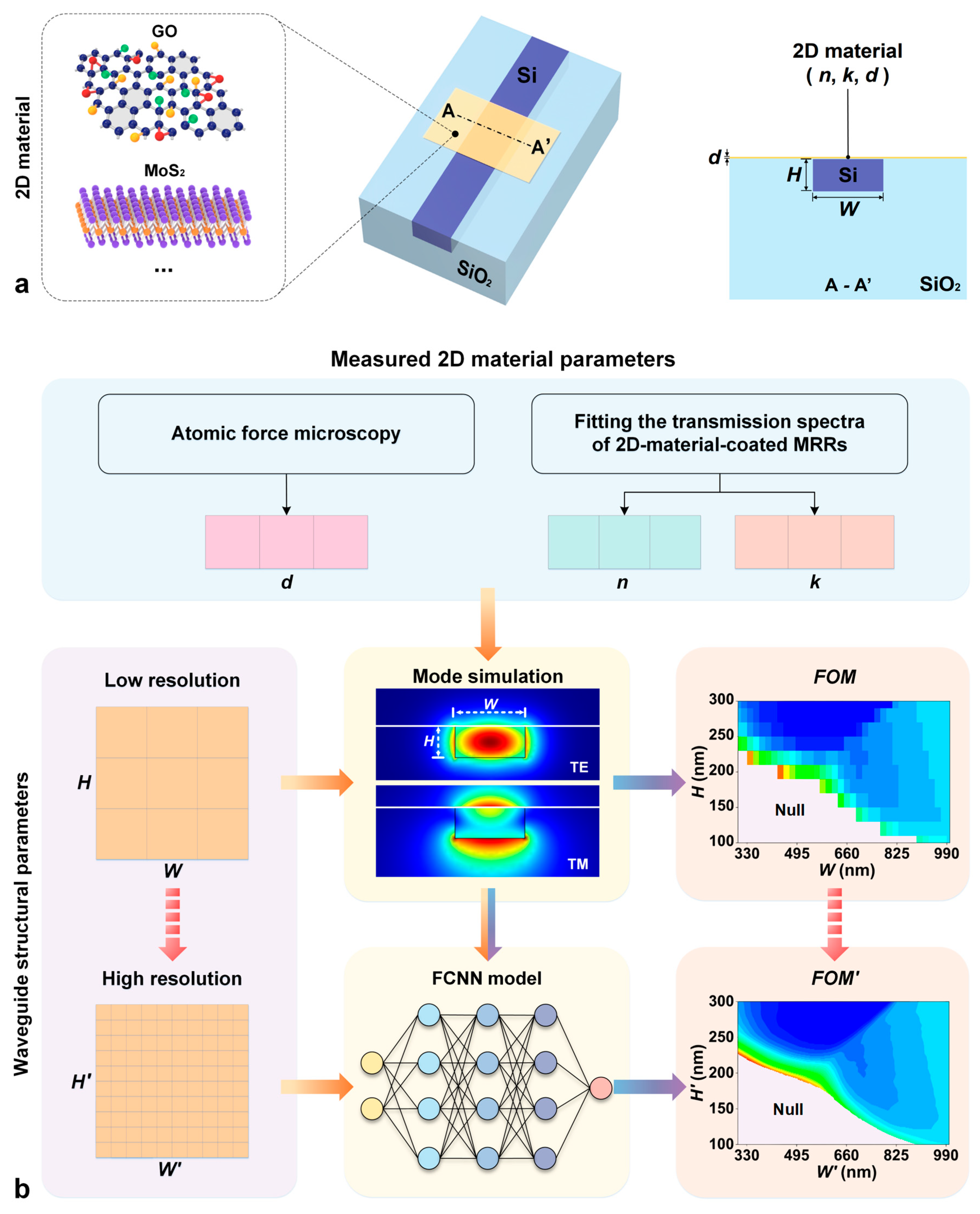
Figure 2.
| a, Schematic illustration of the framework of the FCNN model, which consists of two subnetworks FCNN-1 and FCNN-2 for identifying mode convergence and predicting polarizer FOM’s, respectively. Inset in the right panel illustrates the architecture of FCNN-1, which includes an input layer (L = 1), multiple hidden layers (L = 2, 3, …, m-1), and an output layer (L = m). b, Schematic of a single neuron in FCNN-1, as marked by the dashed box in a. c, Binary cross-entropy (BCE) loss and accuracy versus epoch for the training and validation datasets in training FCNN-1. d, Root mean square error (RMSE) and R2-score versus epoch for the training and validation datasets in training FCNN-2.
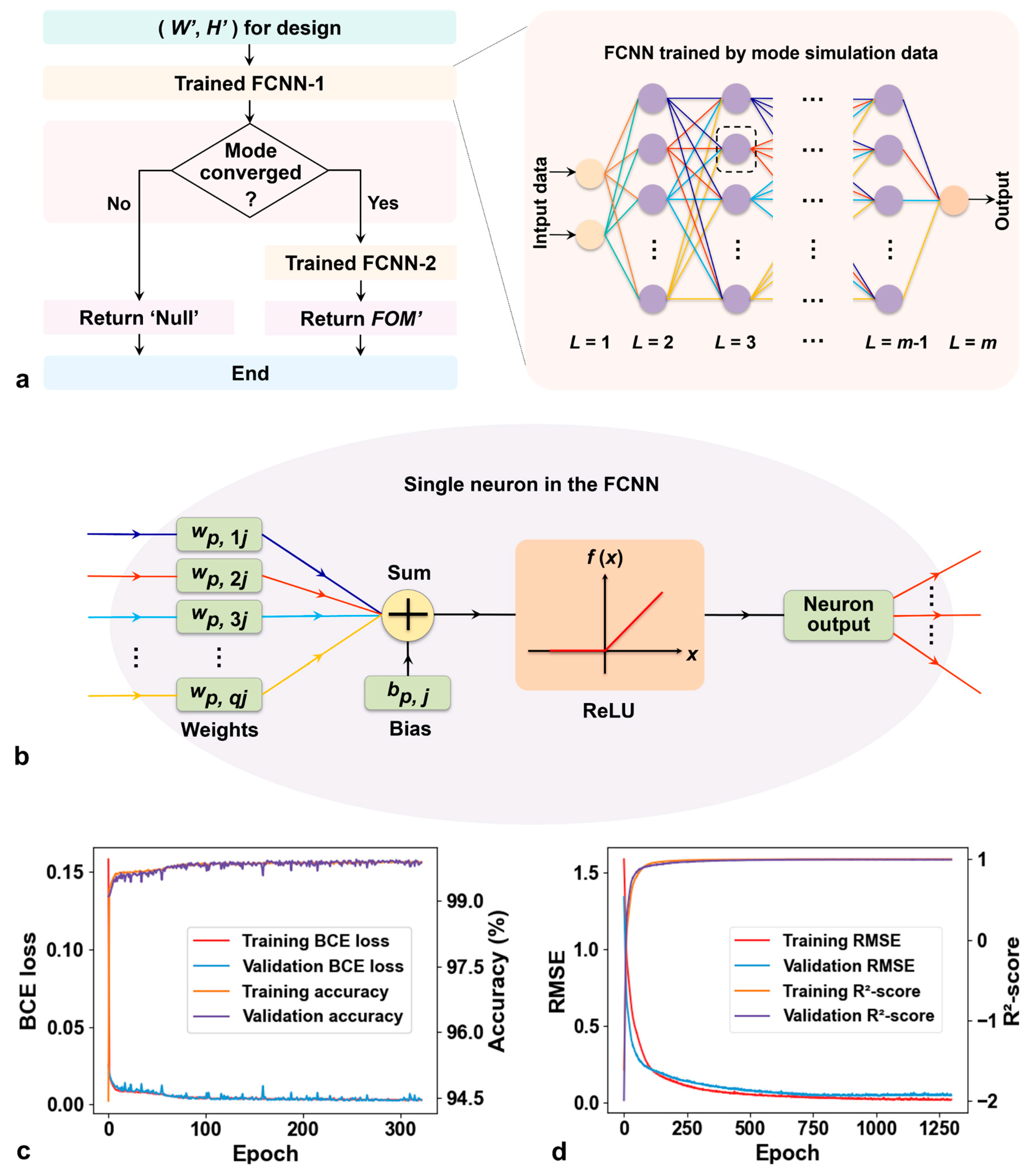
Figure 3.
| a, c, e,FOM of GO-Si waveguide polarizer versus low-resolution (W, H) with Δ = 80 nm, 40 nm, and 20 nm, respectively, where Δ is the step size between adjacent waveguide parameters within ranges of W ∈ [300, 1000] nm and H ∈ [100, 300] nm. The FOM values were calculated based on mode simulations and the ‘Null’ regions denote the cases of non-converged TE or TM modes in the simulations. b, d, f, FOM’ versus high-resolution (W’, H’) with Δ’ = 1 nm. The FOM’ values were predicted using FCNN-2, which was trained by using the data in a, c, e, respectively. The ‘Null’ regions denote the cases of non-converged TE or TM modes, which were predicted using FCNN-1. g, Accuracy of FCNN-1 and average deviation (AD) of FCNN-2 versus Δ. h, TE and TM mode profiles corresponding to a high- and a low-FOM’ point in f, marked by ‘*’ and ‘+’, respectively.
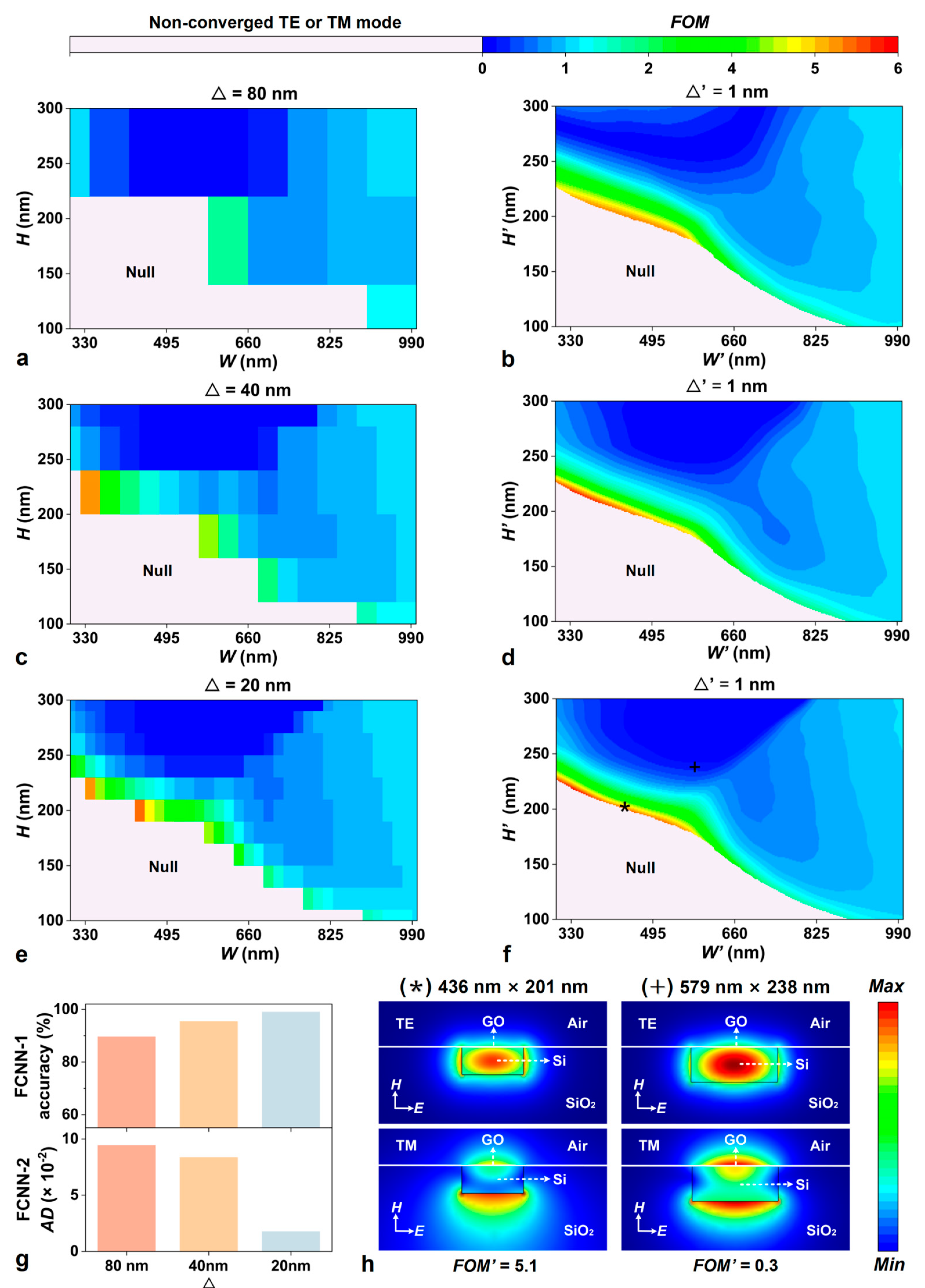
Figure 4.
| a,FOM of GO-Si waveguide polarizer versus low-resolution (W, H) with Δ = 20 nm. The FOM values were calculated based on mode simulations and the ‘Null’ regions denote the cases of non-converged TE or TM modes in the simulations. b, c, d, e, FOM’ versus high-resolution (W’, H’) with Δ’ = 10 nm, 5 nm, 2 nm, 1 nm, respectively. The FOM’ values were predicted using FCNN-2, which was trained by using the data in a. The ‘Null’ regions represent the cases of non-converged TE or TM modes, which were predicted using FCNN-1. f, Accuracy of FCNN-1 and AD of FCNN-2 versus Δ’.
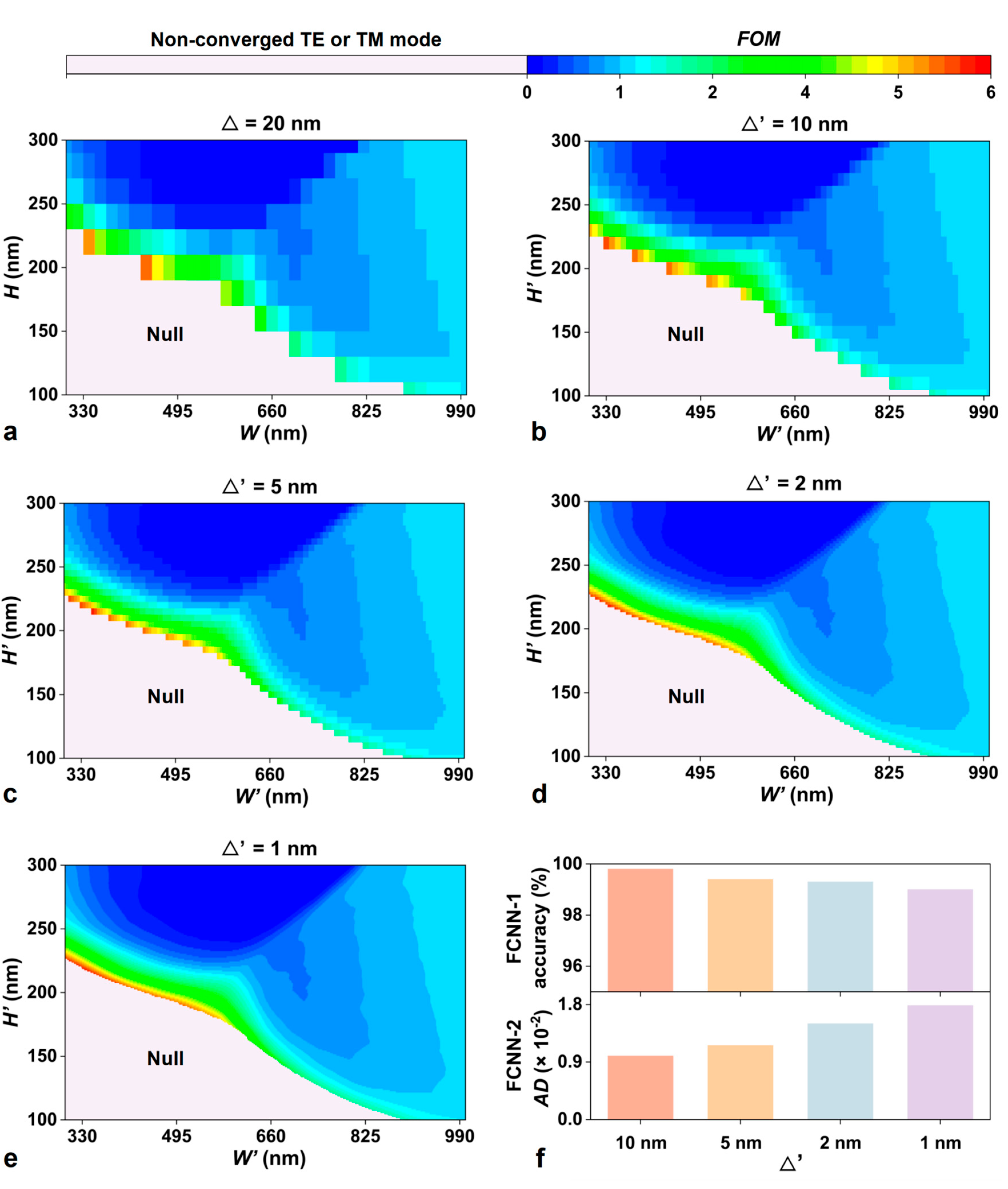
Figure 5.
| a,FOM of MoS2-Si waveguide polarizer versus low-resolution (W, H) with Δ = 20 nm. The FOM values were calculated based on mode simulations and the ‘Null’ regions denote the cases of non-converged TE or TM modes in the simulations. b, FOM’ versus high-resolution (W’, H’) with Δ’ = 1 nm. The FOM’ values were predicted using FCNN-2, which was trained by using the data in a. The ‘Null’ regions represent the cases of non-converged TE or TM modes, which were predicted using FCNN-1. c, TE and TM mode profiles corresponding to a high- and a low-FOM’ point in b, marked by ‘*’ and ‘+’, respectively. d, Comparison of the AD of FCNN-2 between GO-Si and MoS2-Si polarizers.
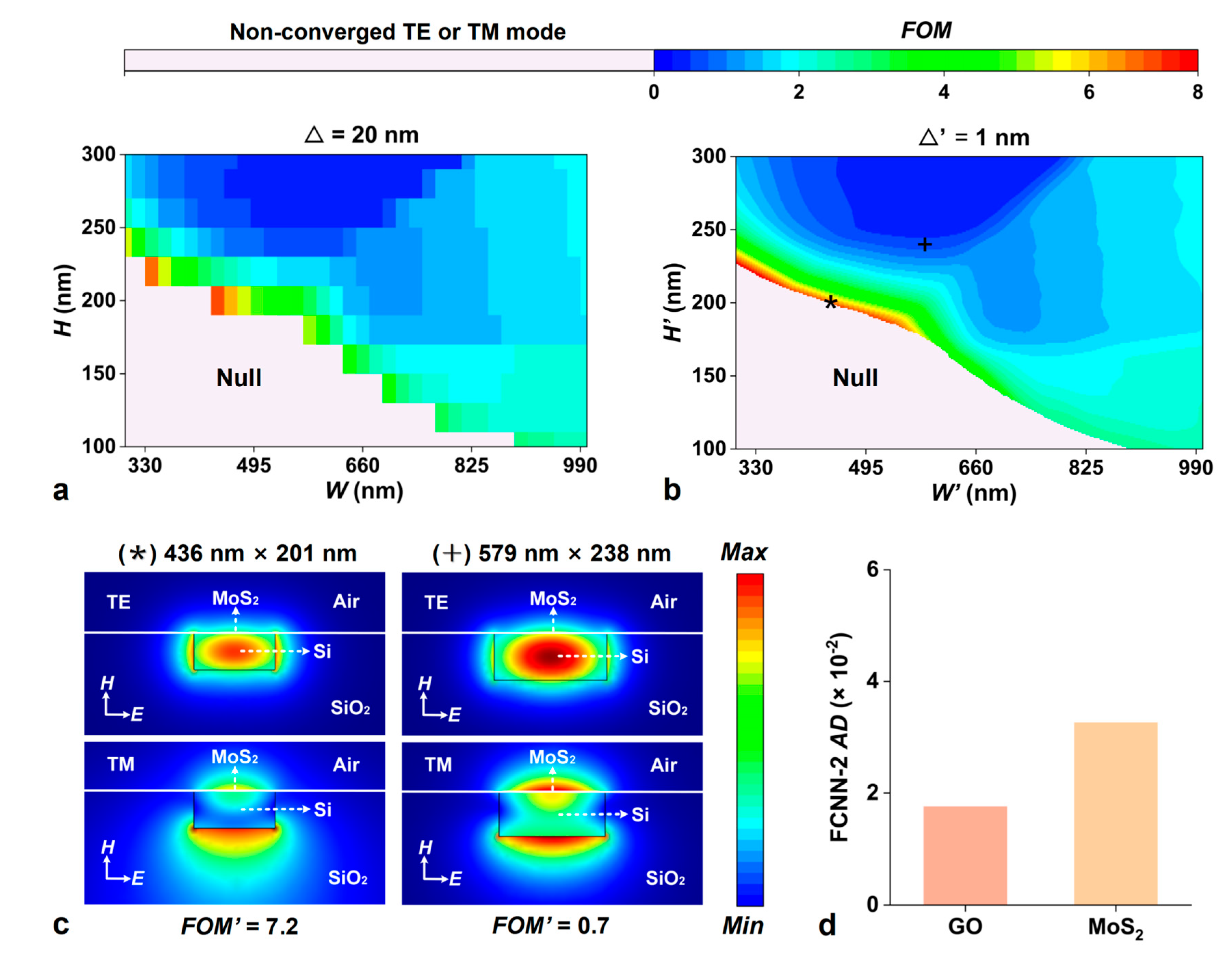
Figure 6.
| a, Comparison of single-point computing times (across 10 tests) between the mode simulation and the machine learning methods. b, Overall computing time of the FCNN model for all (W’, H’) in the test dataset with a step size of Δ’ = 1 nm versus step size of Δ for (W, H) in the training dataset. In a and b, the results for FCNN model include two curves: one corresponds to predictions of mode convergence using only FCNN-1, the other corresponds to predictions of FOM’ using both FCNN-1 and FCNN-2. c, Accuracy of FCNN-1 versus Δ. d, Confusion matrix of FCNN-1 corresponding to point in the dashed circle marked in c. e, AD of FCNN-2 versus Δ for GO-Si and MoS2-Si polarizers. f, Comparison between FCNN-2 predictions and mode simulation results for the points in the dashed circle marked in e. Each dot represents one data point, and the black dashed line indicates the diagonal reference.
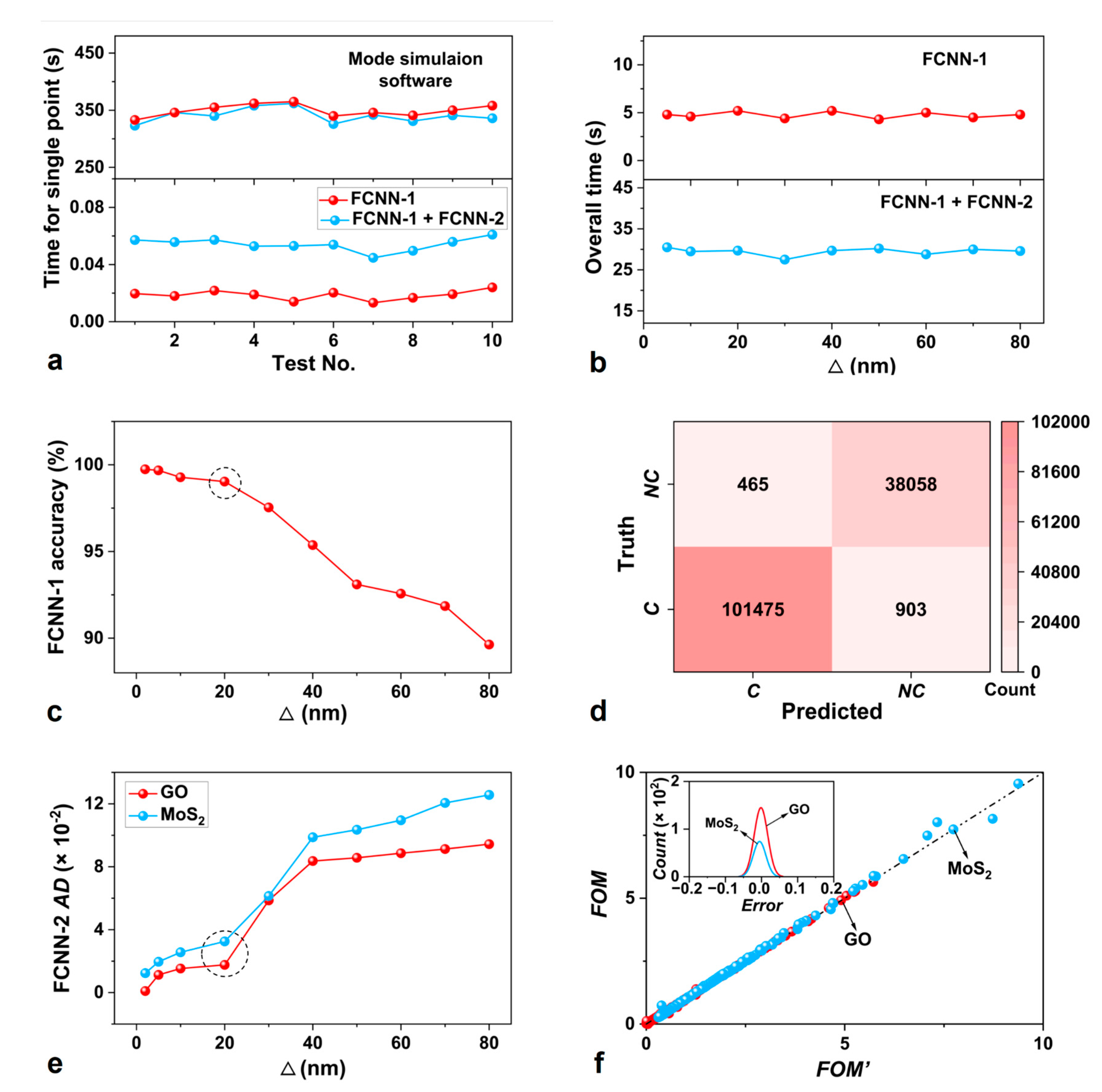
Figure 7.
| a, b, Microscopic images of fabricated GO-Si and MoS2-Si waveguide polarizers on silicon-on-insulator (SOI) chips, respectively. c, d, Measured Raman spectra of SOI chips before and after coating 2D GO and MoS2 films, respectively. e, f, Experimentally measured FOM (Exp.) and FOM’ predicted by the FCNN model (FCNN) versus Si waveguide width (W) for the GO-Si and MoS2-Si polarizers, respectively. In c and d, the Si waveguide height is H = 220 nm.
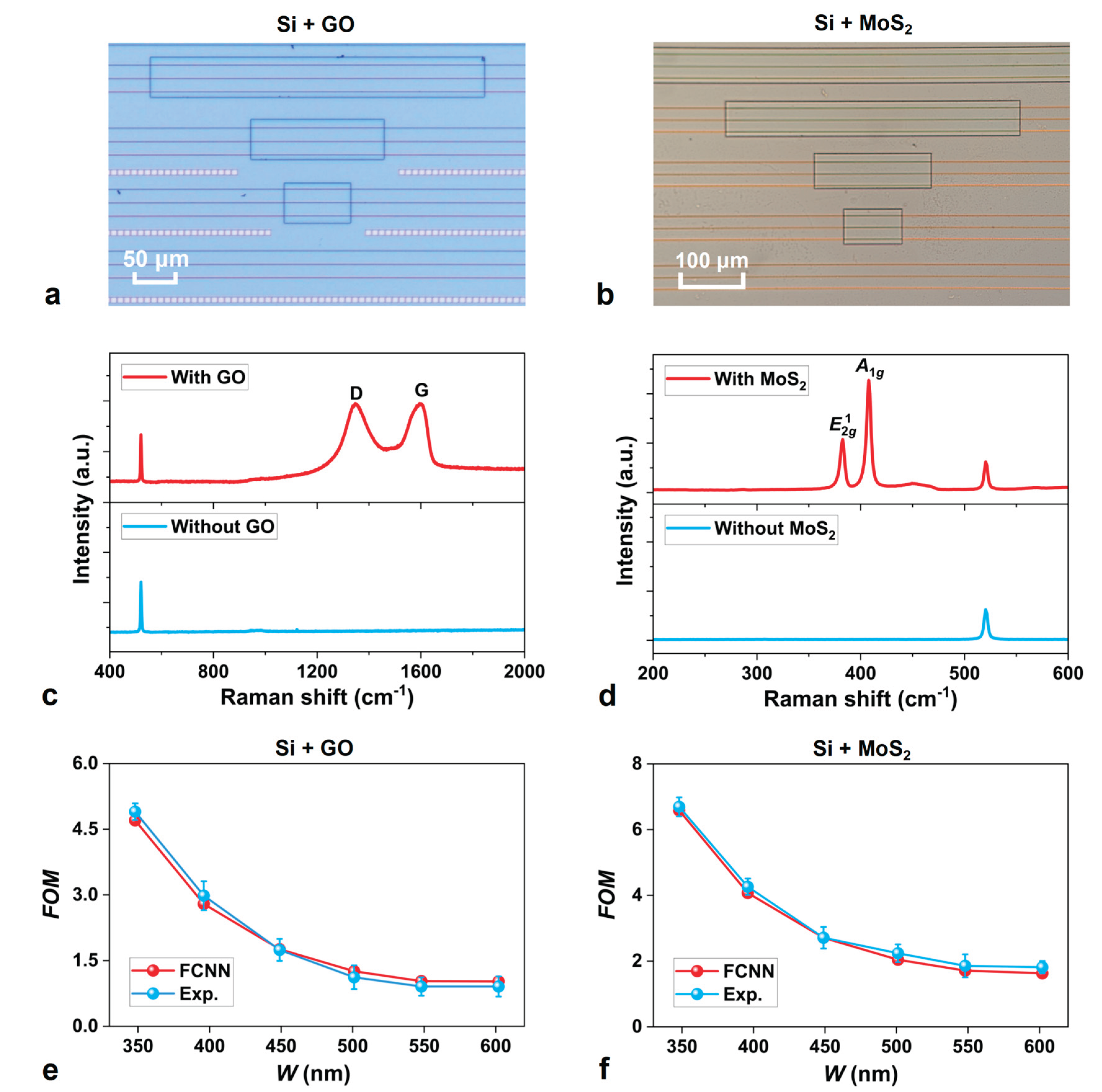
Disclaimer/Publisher’s Note: The statements, opinions and data contained in all publications are solely those of the individual author(s) and contributor(s) and not of MDPI and/or the editor(s). MDPI and/or the editor(s) disclaim responsibility for any injury to people or property resulting from any ideas, methods, instructions or products referred to in the content. |
© 2025 by the authors. Licensee MDPI, Basel, Switzerland. This article is an open access article distributed under the terms and conditions of the Creative Commons Attribution (CC BY) license (http://creativecommons.org/licenses/by/4.0/).
Copyright: This open access article is published under a Creative Commons CC BY 4.0 license, which permit the free download, distribution, and reuse, provided that the author and preprint are cited in any reuse.


