
Submitted:
22 December 2025
Posted:
24 December 2025
You are already at the latest version
Abstract
Scanning electron microscopy (SEM) is a powerful tool for the morphological characterization of multiscale nanomaterials, including two-dimensional (2D) systems such as graphene and molybdenum disulfide (MoS₂). However, conventional SEM imaging often struggles to resolve nanoscale features due to limited contrast and depth sensitivity, especially when dealing with ultrathin layers. In this work, we propose and demonstrate a simple yet effective strategy to overcome these limitations by exploiting grazing-incidence (radent) observation, achieved through a controlled tilting of the sample close to 90°. This approach significantly enhances the emission of secondary electrons from near-surface regions, thereby increasing image contrast and revealing morphological details, such as edges, ripples, defects, and overlapping layers, that remain hidden under standard imaging conditions. Optical characterization of the prepared MoS₂ colloids further supports the formation of monolayer and few-layer sheets, validating the structural information obtained from SEM. Interestingly, this approach recalls natural strategies observed in living organisms, where grazing-angle vision improves edge perception and surface recognition and therefore it can be considered as bio-inspired. Beyond its use with MoS₂, this biomimetic methodology offers a versatile and broadly applicable solution for improving morphological analysis of 2D nanomaterials and thin films, providing deeper insights into their structural characterization.
Keywords:
2D nanostructures
; molybdenum disulfide monolayer
; SEM
; depth-of-field
; tilting
; bioinspired approach
1. Introduction
Morphological analysis plays a fundamental role in the study of materials and nanomaterials [1]. For instance, the morphological analysis of a fractured metallic surface (i.e., fractography) allows to establish if an alloy has a ductile or brittle behavior [2]. Indeed, the alloy has fragile behavior in case sharp or conchoidal fracture surfaces are observed, while it has a ductile behavior if plastically deformed surfaces are generated during the fracturing operation. Consequently, it is of pivotal importance to obtain images of the highest quality so that they may include as much as possible clear and detailed morphological information. Such a requirement is even more stringent in case of nanostructured/microstructured systems, where the material behavior is strictly depending on morphology. However, imaging multiscale nanomaterials, combining micrometric and nanometric dimensions remains particularly challenging [3,4]. This dual size scale makes such nanostructures only partially accessible to conventional techniques, like scanning electron microscopy (SEM). Indeed, due to magnification limits, they often fail to fully resolve nanoscale features. For example, two-dimensional (2D) nanostructures, like lamellas, platelets, single sheets, nanobelts, etc. and monodimensional (1D) nanostructures, like wires with infinitesimal diameter, nanorods, etc. are multiscale nanostructures (i.e., both micro- and macro-dimensions are contained in the nanomaterial) and therefore have such a drawback. Therefore, the morphological features of these nanostructures can be visualized by scanning electronic microscopy and other standard microscopy techniques (e.g., digital microscopy, stereomicroscopy, etc.), but it is quite difficult to understand that the observed objects are 2D or 1D (i.e., they have a Z-extension) because of the limited capability of this technique to resolve the nanometric dimensions. Therefore, to meet this need, if possible, some expedients, optimization procedures, and tricks capable to increase the technique sensitivity for imaging the nanometric size must be adopted.
In this context, the development of alternative observation geometries capable of enhancing surface sensitivity and contrast is becoming increasingly relevant. A particularly promising approach is the use of grazing-incidence SEM, a technique inspired by natural visual strategies and optimized for highlighting subtle topographical and morphological features that are otherwise undetectable. Such an approach is especially useful when dealing with ultrathin coatings, interfaces, or 2D nanostructures, where the interplay between micro- and nanoscale features strongly influences material performance.
Electronic microscopies are widely used in the morphological investigation of all material types [5,6]. In particular, SEM microscopy represents a standard technique in material science largely used also because it allows to observe specimens without requiring complex sample preparation procedures. The simplicity of SEM sample preparation is mainly due to its high depth-of-field, i.e. the ability to focus on points at different planes [7]. This SEM feature is very high at low magnifications (1mm at 100X [7]) and gradually reduces with increasing of magnification (however, it results always extremely high compared to other microscopic analysis techniques like the optical microscopy, stereomicroscopy, transmission electron microscopy, etc.).
This peculiarity of SEM imaging allows optimizing the observation by a sample tilting operation, which is practically impossible with other microscopy techniques. Tilting the sample relative to the electron beam-detector axis enhances the emission of secondary electrons (SE), improving the image quality (contrast). Since image quality is directly correlated with the number of SE reaching the detector, an increase in contrast upon tilting implies a higher SE yield (number of SE per primary electron, PE). This enhancement arises from the geometry of electron–sample interaction, which can be optimized by adjusting the sample inclination within the limits imposed by the depth of field. Beyond improving conventional imaging, this methodology can provide fundamental morphological insights into materials whose function relies on nanoscale organization — such as catalytic surfaces, functional coatings, or layered 2D systems like MoS₂. Its application thus bridges the gap between classical SEM imaging and advanced morphological analysis, offering a versatile tool for materials science and biomimetic engineering.
SE are emitted by direct collision between primary electrons (PEs) and the electron belonging to the atom. Generated SEs have very low energy values (usually less than 30eV [8]) and consequently come out from the sample only if produced close to the surface [9]. In order to generate them as close as possible to the surface, the incident PEs beam must be as grazing as possible, so that the full path of the incident beam in the material is located in an immediately sub-surface region. Indeed, the distance of the deepest point reached by primary electrons is given by the product between penetration depth (d) and sin of the grazing angle α (which is complementary to the incidence angle, θ). When this quantity is close to zero, the distance of SE from the surface is negligible and therefore all SEs generated in the PEs crossing the material escape from the sample surface. Such a behavior involves the maximum yield of SE; however, since the depth-of-field has always some limitations, the best sample inclination must necessarily be a compromise between these two quantities (i.e., maximum inclination with completely sharp visual field).
The objective of this work is to demonstrate how a controlled grazing-incidence SEM observation significantly improves morphological contrast and information content in the study of multiscale nanomaterials. We illustrate this approach through the case study of MoS₂, showing how complementary optical spectroscopy analyses confirm the structural features revealed by the SEM observations. The strategy proposed here not only deepens the fundamental understanding of 2D materials but also provides a methodological framework that can be extended to a broad range of coatings and nanostructured surfaces.
In this manuscript, in order to establish the capability of this approach to improve image quality, SEM micrographs obtained by the ~90°-tilting approach have been compared with that resulting from standard SEM observations (that is, performed without any sample tilting). In particular, contrast quality in SEM micrographs obtained in presence and absence of tilting has been quantified by measuring the amount of grey levels involved in these micrographs. According to such image analysis, the tilting operation has caused a significant increase of the amount of morphological features visualized in the micrographs.
2. Materials and Methods
2.1. Preparation and Optical Characterization of MoS₂ Colloidal Suspensions
Owing to its layered structure, MoS2 can be exfoliated by the combined action of mechanical shear and sonoacoustic energy to originate monolayer and/or few layer nanosheets. Commercial powder of MoS2 (98% by weight, average size of 4-5 µm, Werth-Metall, Grammental, Germany) has been used as starting material for the preparation of colloidal suspensions. Morphology and size of the as-received powder have been investigated by SEM imaging at different magnifications (see Figure 1a,b,c). The chemical composition of this powder has been established by energy dispersive X-ray spectroscopy (EDS, see Figure 1c). Accordingly, the MoS2 grains have a layered structure and contains little amount of copper and iron as impurities.
In the preparation of colloidal suspensions, the as-received MoS2 powder underwent a preventive mechanical treatment. This mechanical treatment was based on the application of shear stress to the basal planes of the micrometric lamellar crystals to convert them to small platelets. Internal coherency in these small crystalline platelets results much lower than in the starting micrometric lamellas, thus allowing their easy sonoacoustic exfoliation. In particular, the as-received powder was slightly pressed between two circularly moving surfaces of polytetrafluoroethylene (PTFE). While sandpaper has been previously reported for a similar purpose [10], PTFE was preferred here to minimize contamination. This mechanical pretreatment is of pivotal importance, as sonication alone does not effectively induces exfoliation.
Following mechanical pre-treatment, the powder was dispersed in high-purity acetonitrile (CH3CN, HPLC grade, J.T. Baker, London, UK) [11], and the obtained suspension was taken for a few hours in a sonication bath (ultrasonic bath with built-in heating SONOREXTM SUPER, Bandelin, Berlin, Germany) in order to convert the MoS2 platelets to a mixture of mono-layers and few-layer nanocrystals. Sonication was performed for 2h, taking the liquid sample in a closed glass vial.
To further purify the dispersion and selectively isolate few-layer crystals of MoS2, the achieved colloidal suspension was diluted with additional pure acetonitrile and sonicated under identical conditions (see Figure 2a). Then, the diluted suspension was left to settle for a few weeks. The concentrated MoS2 colloidal suspension was stable due to electrostatic repulsion between charged nanosheets. Dilution increased interparticle spacing and promoted sedimentation of larger particles. After settling, the supernatant was carefully collected by decantation and used for subsequent analyses. The colloids were optically characterized by UV-Vis spectroscopy (PerkinElmer Lambda 850 spectrophotometer) in order to establish the presence of MoS2 monolayers.
2.2. Sample Preparation for SEM Analysis
Samples for SEM characterization were prepared by drop-casting small volumes of liquid supernatant onto clean glass substrates. The solvent (acetonitrile) was allowed to evaporate under ambient conditions, leaving a thin film of dispersed MoS₂ nanosheets on the substrate surface. The morphological characterization was performed by using scanning electron microscopy (SEM, Quanta 200 FEG microscope, FEI, Eindhoven, The Netherland). Prior to SEM observations, all samples were sputter-coated with a thin Au-Pd alloy layer to increase surface electrical conductivity and adhesion to the substrate.
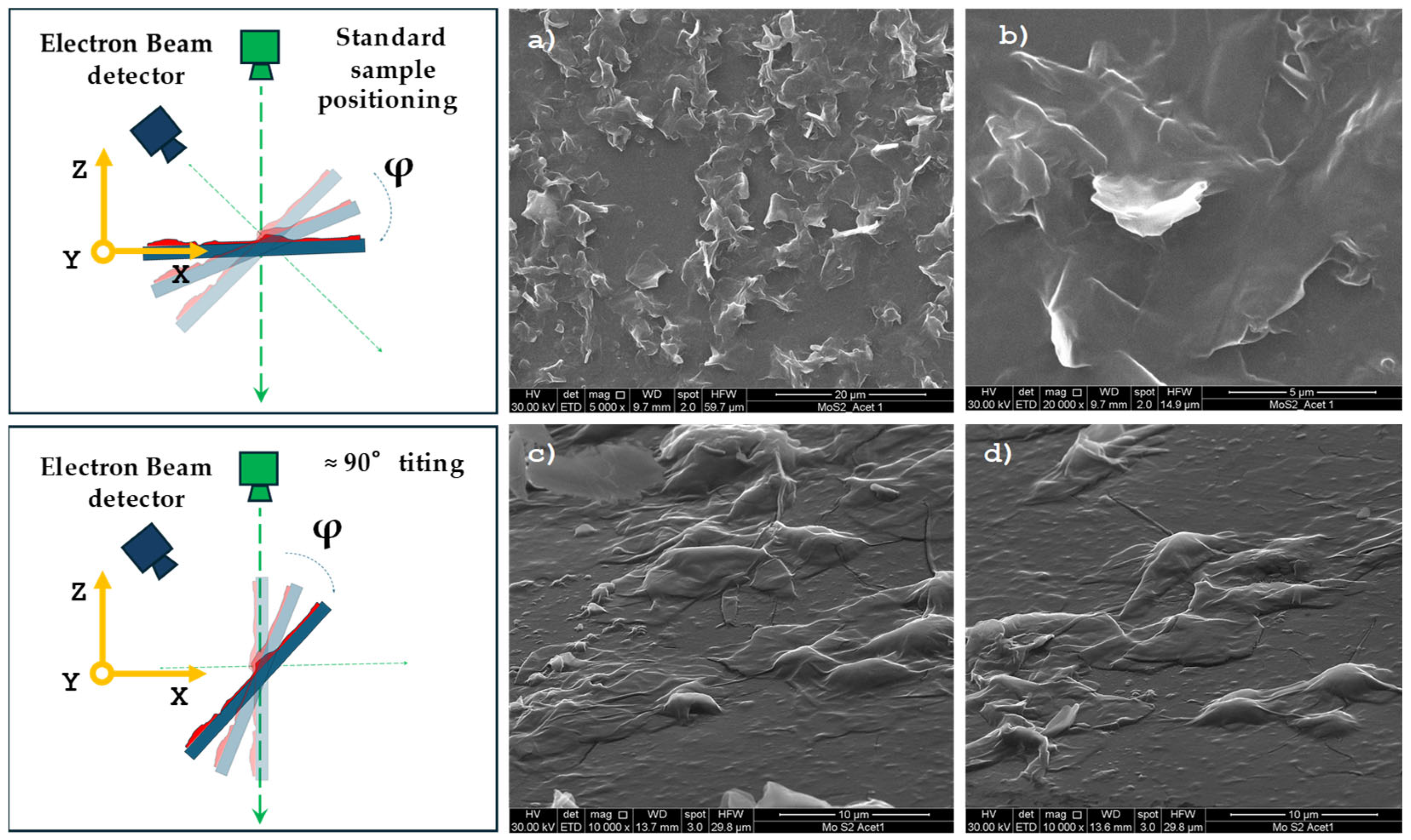
During the morphological investigation, each sample was examined under two distinct imaging geometries: (i) standard positioning (0°-tilting), and (ii) grazing-incidence configuration (~90°-tilting). For the 0°-tilting observations, a standard aluminum pin stub was used, while for the ~90°-tilting observations a stable vertical sample positioning was achieved by using a special aluminum slotted specimen stub (slot diameter: 12.5mm, with a 4mm wide cavity, and height: 10mm; an allen kay is present in this stub, see Figure 2).
SEM micrographs were analyzed by using the Image J 1.48v software, NIH (National Institutes of Health, Bethesda, MD, USA) [12]. This software is an open-source image processing application, designed to analyze multidimensional scientific images, like the SEM micrographs. Image analysis was performed on areas containing an identical number of pixels to ensure quantitative comparability.
3. Results
3.1. Optical Characterization of MoS₂ Colloids
This optical characterization was carried out to verify the presence of MoS2 monolayers in the prepared colloidal samples. In particular, the SEM technique, we are proposing here, is particularly adequate for observing multiscale nanostructures, like MoS2 monolayers; indeed, the morphological characterization of such type of 2D nanostructures could widely benefit of an increased sensitivity along the Z direction, which has a nanometric size (thickness). Consequently, it is very important to prove the monolayer nature of the produced samples that can be easily done spectroscopically (i.e., by absorption optical spectroscopy). Both the presence of specific absorption bands and the measurement of the related bandgap energy values prove that the preparation method and in particular the settling stage has led to MoS2 monolayers. It must be pointed out, that MoS2 has useful optical and electronic properties only in the case it is in a monolayer form. Figure 3a shows the optical absorption spectrum of the colloidal suspension of MoS₂ in acetonitrile. This spectrum reveals the presence of three well-defined bands centered at approximately 680 nm, 622 nm and 458 nm, corresponding to photon energies of 1.82 eV, 1.99 eV, and 2.71 eV, respectively. These absorption bands correspond to well-established optical transitions in mono-layer and few-layers MoS₂ and are generated by interband transitions [13,14].
Specifically, the absorption bands at 680 nm (band A) and 622 nm (band B) are assigned to the so-called A and B absorptions, which originate from the direct transitions at the K-point of the Brillouin zone (see scheme shown in Figure 3b) [15]. These absorptions arise from the spin–orbit splitting of the valence band, which is particularly significant in transition metal dichalcogenides (TMDs) due to the heavy transition metal atoms. The A absorption (at 1.82 eV) involves transitions from the upper valence band (with lower spin) to the conduction band minimum, while the B absorption (at 1.99 eV) originates from the lower valence band (with higher spin) to the same conduction band minimum. The energy separation between the A and B absorptions in this spectrum is approximately 0.17 eV, which is in agreement with theoretical predictions and previous experimental reports for MoS₂ monolayers [13,16]. The presence of well-resolved A and B absorption bands suggests that the MoS₂ flakes in the colloid are predominantly monolayers or few-layers in nature. The third absorption band, located at 458 nm (2.71 eV), indicated as band C in Figure 3a, is associated with transitions involving higher-energy states in the Brillouin zone. This band is attributed to a phenomenon known as ‘band nesting’, which indicates that parallel bands in the electronic structure lead to a high joint density of states and enhanced optical absorption. The observation of this peak further supports the presence of well-dispersed, crystalline MoS₂ nanosheets in the prepared colloid.
A simple linear model can be used to estimate the average number of layers (N) in the nanoparticle from the A absorption energy value (EA) [17]:
where Ebulk = 1.29 eV (bulk MoS₂), K = 0.8 eV (empirical constant). Replacing the measured EA value of 1.82 eV (absorption energy of the A band in our sample), it yields N ≈1.5, thus confirming the presence of MoS₂ monolayers as predominant specie in the obtained colloidal suspension with a minor amount of MoS2 bilayers [13].
EA(N) = Ebulk + K/N
The bandgap energy of the MoS₂ colloid, Eg = 1.37 eV, has been optically estimated by using the modified Tauc plot method [18] based on the data in the optical absorbance spectrum (see Figure 4). The Tauc plot was constructed using the absorbance (A) values directly, without conversion to the absorption coefficient, α, since the effective optical path length is unknown for colloidal systems. This approach is particularly suitable for colloidal systems where the exact concentration and path length may not be precisely known or controlled.
According to the literature, the direct allowed electronic transitions model better describes this colloidal MoS2 semiconductor and the Tauc equation written by using the absorbance for this model is typically expressed as:
(Ahν)2∝ (hν−Eg)
In more detail, this method assumes that absorbance is proportional to the absorption coefficient (i.e., A∝α), and is valid for a qualitative estimation of the optical bandgap. The vertical axis of the plot was expressed in units of (eV)2, as recommended in the recent literature [13], avoiding the incorrect use of arbitrary units or units involving cm⁻¹, which would imply a path-length-dependent α value. The linear portion of the (Ahν)2 vs. hν plot was extrapolated to the energy axis to determine the optical bandgap. This optical bandgap value estimated from the modified Tauc plot is approximately 1.37 eV (Figure 4). This value is lower than the A absorption energy (1.82 eV), as expected, since the absorption band includes electron–hole binding energy and does not directly correspond to the fundamental bandgap. This is consistent with the A absorption observed at 680 nm (1.82 eV), supporting the presence of monolayer or few-layer MoS₂ in the prepared colloidal sample.
The optical bandgap extracted from the Tauc plot is lower than the A-exciton energy, but this behavior is expected for colloidal MoS₂ dispersions. In these suspensions, the absorption onset is dominated by few-layer nanosheets, which possess lower indirect bandgaps in the range 1.3–1.5 eV, through PL and photoconductivity analysis of 2–6 layer MoS₂ [13]. Moreover, defect-related tail states introduced during liquid-phase exfoliation cause additional sub-gap absorption, further lowering the apparent optical onset, consistently with reports of defect-induced PL bands below the A-exciton [15]. Finally, the A-exciton energy does not represent the fundamental bandgap, since it includes the exciton binding energy, typically 0.3–0.5 eV in monolayer MoS₂. Accounting for these effects, the observed Tauc intercept at 1.37 eV is fully consistent with a polydisperse MoS₂ colloid composed of monolayer and few-layer flakes.
3.2. Application of the Tilting Method to the MoS2 Mono-Layer Observation
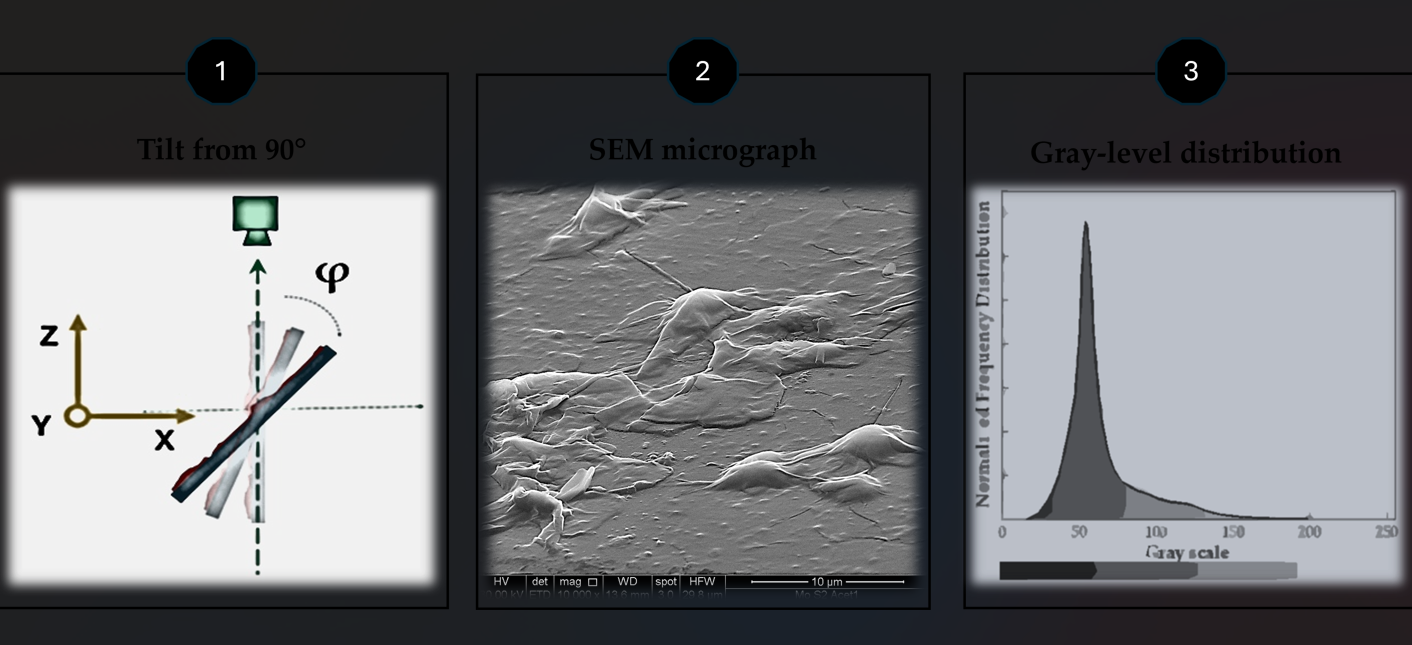
A comparison between the SEM micrographs of MoS2 monolayers placed on a flat glass surface and imaged as both non-tilted and ~90°-tilted views is shown in Figure 5. As clearly visible, the contrast in the SEM micrographs obtained by these two types of observations differs significantly. Standard non-tilted images (see Figure 5a,b) are characterized by a contrast level much lower than that characterizing ~90°-tilted views (see Figure 5c,d). The tilted configuration produced images with significantly enhanced contrast, characterized by a broader distribution of grey levels and improved visibility of nanoscale morphological features (e.g., ripples, bendings, fractures, porosities).
The limited greyscale range in non-tilted observations makes it difficult to distinguish fine surface features. Differently, high-contrasted images can provide a large amount of topological information on the investigated samples.
Qualitatively, the ~90°-tilted micrographs revealed structural details, such as nanosheet edges, overlapping regions, ripples, defects, pores, and fracture sites, that were indistinguishable in standard SEM images. Enhanced contrast also allowed visualization of subsurface features and thickness variations, which are crucial for the structural assessment of ultrathin 2D materials.
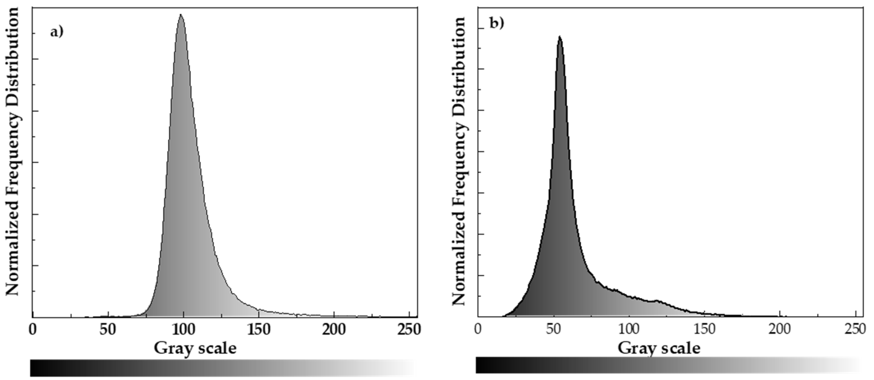
The above considerations can be quantitatively confirmed through the image analysis of these SEM micrographs, i.e. by evaluating the different grey levels present in these SEM micrographs. Grey levels in the micrographs of the non-tilted and ~90°-tilted samples were analyzed with an image analysis software, and the obtained results are shown in Figure 6. To make comparable the SEM micrographs of the samples obtained with and without tilting, images containing the same number of pixels were analyzed by measuring the percentages of all grey levels present in them. Then, the achieved histograms were normalized with respect to the maximum intensity (the intensity of the most abundant grey level visible in the image). Such normalization allowed for the correct visualization of the number of grey levels contained in each graph. The number of grey levels grew from 169 (Figure 6a) to 237 (Figure 6b), which corresponds to an increase of 40.2%. In addition, in this case, we measured the area below each curve, finding a 30.1% increase in this area. Therefore, it is evident from such results that the ~90°-tilting operation significantly increases this image contrast.
This contrast enhancement obtained by applying a significant tilting to the 2D nanostructures (i.e., close to 90°) is due to the higher yield of SEs per PE, which results in a SE emission occurring in a region of the sample closer to the surface. In fact, SEs usually have low energy values, and therefore, they can escape the sample only in the case they are produced very close to the surface. An immediate sub-surface emission is achieved with the grazing incidence of the PE beam. In contrast, a vertical PE beam incidence causes SE emission from deep sample regions with consequent yield decrease.
4. Discussion
The results presented in this study demonstrate that SEM imaging performed under grazing-incidence conditions (~90°-tilting) significantly improves the morphological contrast of ultrathin MoS₂ nanosheets compared to conventional 0°-tilt imaging. This enhanced contrast enables the visualization of features such as sheet edges, folds, wrinkles, overlapping regions, thickness variations, pores, and fracture sites, which are largely undetectable under standard SEM geometry.
The grazing optical observation is a special visualization approach widely adopted in nature by the living creatures [20,21,22,23,24,25]; however, when visible photons are used to get optimized images, a working principle different from that involved in the SEM observation is active. Indeed, in the visible light oblique observation contrast is increased because of the shadowing, which is capable of better define the feature contours that are generated. In more detail, the vision is a phenomenon based on the reflection of visible light at interface between two phases, that is, the solid sample surface and the air. A photon source and a detector, which is the eye, are required to perform the vision. Eyes are capable to collect light reflected by the sample surface independently from the orientation of the light source; however, visual acuity strictly depends on the relative positioning of light source and eyes. It is possible to strongly increase the visual acuity by adopting a grazing orientations of a perfectly collimated photon beam coming out from the light source respect to the surface to be observed and observing this lighted surface by using the eyes placed perpendicularly to the photon beam. Such type of observation is named ‘grazing observation’ and it is largely adopted also in modern architecture and light technology. The special approach of ‘grazing observation’ works very well because in such a way very long shadows are generated by the impact of photons on the surface roughness (visual acuity is increased proportionally to the grazing of the photonic beam on the surface asperities). Shadows clearly define the contour of each minimal asperity since they thicken them and therefore highlight the details, thus resulting in an exceptional image contrast enhancement.
In SEM observations it is the oblique positioning of the detector and PE beam respect to the sample surface (that is, the ~90°-tilting of the sample) to improve image quality; indeed, it allows to generate and collect an extremely large number of SE coming out from the sample surface [26]. However, in both situations it is the grazing orientation of the radiation source to produce higher contrasted images, in one case by the reflection mechanism (visible photons) and in the other case by a stronger SE emission (SEM observation).
Such a behavior can be easily understood on the basis of the following geometrical consideration. The SE path (x) in the sample subsurface region depends on the PE penetration depth (d) and on its incidence angle value (α), as x = d·sin(α).
The relative variation of the SE path (Δx/x) as a function of the incidence angle relative variation (Δα/α) is Δx/x = [cos(α)/sin(α)]·Δα/α. In the case of a very shallow angle of incidence (α≈0), the cos(α) value can be taken as approximately equal to 1 and the sin(α) value can be approximated by α. Therefore, Δx/x ≈ (1/α)·Δα/α. Since α is quite close to zero, the 1/α value is extremely large and therefore a significant relative variation of the SE path is obtained as a result of a small variation of the grazing angle. Under extreme grazing conditions (i.e., a sample surface almost vertically positioned), a little increase in the tilting angle (α decreases) determines an important decrease in the SE path. Since SE has a very low energy value (usually less than 30eV), they rapidly extinguish moving through the sample subsurface region and therefore a significant reduction of the path length by sample tilting from the vertical position may strongly increase the quantity of SE escaping the surface and therefore the quality of the micrograph (contrast level). Indeed, in the hypothesis that the number of emitted secondary electrons, NSE, is inversely proportional to the distance from the surface, x, it results: ΔNSE/NSE ≈ - (1/α)·Δα/α. The only limitation in this tilting operation is represented by the sharpness of the observation field that must be retained during the observation in tilting conditions. In particular, the tilting degree must be as high as possible, however it does not have to compromise the SEM image sharpness.
It is also important to note that, unlike grazing-incidence X-ray scattering, where coherent photon-matter interaction leads to interference or diffraction features, secondary electron emission in SEM is incoherent. SEs result from localized inelastic collisions and have low energies (<30 eV), short mean free paths and randomized phases. Consequently, no diffraction-like effects can form at the detector. Nevertheless, under grazing incidence the SE signal may exhibit small intensity fluctuations due to geometric factors, such as variations in local surface slope, roughness, or changes in escape probability, rather than true interference phenomena.
Compared to previous approaches that attempt to enhance SEM contrast through variations of accelerating voltage, detector positioning or surface metallization, the method proposed here is simpler, non-destructive and does not require instrument modification. Furthermore, it is conceptually related to natural optical strategies based on grazing illumination, adopted in biological systems to improve edge recognition and surface defect detection. In contrast to optical systems, however, the mechanism active in SEM is not shadow formation but maximization of SE collection from near-surface regions.
This methodology is particularly advantageous for two-dimensional materials and ultrathin coatings, whose functional properties strongly depend on nanoscale morphology. Although the technique may be less effective for thick, highly corrugated or insulating samples, where shadowing effects or charging may occur, it remains broadly applicable to other layered systems such as graphene, WS₂, h-BN, and to nanostructured films and biomimetic surfaces.
The SEM observation approach we propose, based on an almost vertical sample positioning, has only few practical limitations and can be applied in most cases. For example, a strong sample tilting reduces the maximum applicable magnification during the morphological investigation. In particular, in the SEM technique, the depth-of-field strictly depends on magnification and precisely it rapidly reduces with increasing of magnification. Therefore, exhaustive tilting observations cannot be adequately applied in case of morphological investigations requiring the highest microscope performance in terms of magnification. The proposed technique perfectly applies to the 2D and 1D nanomaterials case because these types of nanostructures have hundred microns sized main dimensions and therefore can be perfectly visualized also at low magnifications. Differently, morphological investigation of randomly distributed 0D-nanostructures (i.e., variously shaped particles like spheres, cubes, etc.) benefits nowise of an exhaustive sample tilting. If magnification is not adequately reduced, the observation field does not result perfectly sharp and focusing involves only a portion of the observation field (typically, the central part).
5. Conclusions
In this work, a grazing-incidence SEM strategy based on ~90°-sample tilting was demonstrated to significantly enhance morphological contrast in two-dimensional MoS₂ nanosheets. Compared to conventional imaging with a tilt of 0°, this approach increases the number of detectable grey levels by more than 40% and reveals structural details such as sheet edges, folds, overlaps, pores and defects that are otherwise invisible.
The contrast enhancement originates from a higher secondary-electron yield, due to the reduced penetration depth of primary electrons and the more efficient escape of SEs from near-surface regions. This effect is achieved without loss of image sharpness, taking advantage of the intrinsic high depth-of-field of SEM.
The proposed method is simple, non-destructive and does not require instrumental modifications, making it suitable for routine SEM analysis of ultrathin 2D materials and nanostructured coatings. Although shadowing effects or reduced effectiveness may occur in thick or highly corrugated samples, the approach is widely applicable to other layered materials (e.g., graphene, h-BN, WS₂) and bio-inspired interfaces.
Author Contributions
all authors have contributed equally to the manuscript preparation.
Funding
The authors acknowledge financial support provided by the National Recovery and Re-silience Plan (NRRP), Mission 4, Component 2, Investment 1.1, Call for tender No. 1409 published on 14 September 2022 by the Italian Ministry of University and Research (MUR), funded by the European Union—NextGenerationEU—Project Title “Development of two-dimensional environ-mental gas nano-sensors with enhanced selectivity through fluctuation spectroscopy (2DEGAS)” Grant P2022S5AN8.
Institutional Review Board Statement
Not applicable.
Informed Consent Statement
Not applicable.
Data Availability Statement
The original contributions presented in this study are included in the article. Further inquiries can be directed to the corresponding author(s).
Acknowledgments
The authors would like to express their sincere gratitude to Mariacristina Del Barone (LaMEST Laboratory, IPCB-CNR) for her valuable support in the SEM characterization.
Conflicts of Interest
The authors declare no conflicts of interest.
References
- Mayeen, A.; Shaji, L.; Nair, A.K.; Kalarikkal, N. Morphological characterization of nanomaterials. In Characterization of nanomaterials; Woodhead Publishing, 2018; pp. 335–364. [Google Scholar]
- Loto, C.A.; Loto, R.T. Failure analysis of metallic materials: morphological characteristics, mechanisms and laboratory investigation. Journal of Bio-and Tribo-Corrosion 2020, 6(2), 57. [Google Scholar] [CrossRef]
- Ko, S.H. Review of the multi-scale nano-structure approach to the development of high efficiency solar cells. Smart Science 2014, 2(2), 54–62. [Google Scholar] [CrossRef]
- Zhang, X.; Wang, N.; Li, Y. The accurate synthesis of a multiscale metallic interface on graphdiyne. Small Methods 2024, 9(2), 2301571. [Google Scholar] [CrossRef] [PubMed]
- Liu, F.; Wu, J.; Chen, K.; Xue, D. Morphology study by using scanning electron microscopy. In Microscopy: Science, Technology, Applications and Education; Méndez-Vilas, A., Diaz, J., Eds.; 2010; pp. 1781–1792. [Google Scholar]
- Ortiz Ortega, E.; Hosseinian, H.; Rosales López, M.J.; Rodríguez Vera, A.; Hosseini, S. Characterization techniques for morphology analysis. In Material Characterization Techniques and Applications; Springer Singapore: Singapore, 2022; pp. 1–45. [Google Scholar]
- Rempfer, G.F.; Nadakavukaren, K.K.; Griffith, O.H. Depth of field in emission microscopy. Ultramicroscopy 1980, 5(4), 449–457. [Google Scholar] [CrossRef]
- Seiler, H. Secondary electron emission in the scanning electron microscope. J. Appl. Phys. 1983, 54(11), R1–R18. [Google Scholar] [CrossRef]
- Abe, K.; Kimura, K.; Tsuruga, Y.; Okada, S.-I.; Suzuki, H.; Kochi, N.; Koike, H.; Hamaguchi, A.; Yamazaki, Y. Three-dimensional measurement by tilting and moving the objective lens in CD-SEM (II). In Metrology, Inspection, and Process Control for Microlithography; SPIE, 2004; XVIII (Vol. 5375, pp. 1112–1117. [Google Scholar]
- Forsberg, V.; Zhang, R.; Bäckström, J.; Dahlström, C.; Andres, B.; Norgren, M.; Andersson, M.; Hummelgard, M.; Olin, H. Exfoliated MoS2 in water without additives. PLoS ONE 2016, 11(4), e0154522. [Google Scholar] [CrossRef]
- Pachauri, V.; Kern, K.; Balasubramanian, K. Chemically exfoliated large-area two-dimensional flakes of molybdenum disulfide for device applications. APL Mater. 2013, 1(3), 032102. [Google Scholar] [CrossRef]
- Schneider, C.A.; Rasband, W.S.; Eliceiri, K.W. NIH Image to ImageJ: 25 Years of Image Analysis. Nat. Methods 2012, 9, 671–675. [Google Scholar] [CrossRef]
- Mak, K.F.; Lee, C.; Hone, J.; Shan, J.; Heinz, T.F. Atomically Thin MoS₂: A New Direct-Gap Semiconductor. Phys. Rev. Lett. 2010, 105(13), 136805. [Google Scholar] [CrossRef]
- Eda, G.; Yamaguchi, H.; Voiry, D.; Fujita, T.; Chen, M.; Chhowalla, M. Photoluminescence from Chemically Exfoliated MoS₂. Nano Lett. 2011, 11(12), 5111–5116. [Google Scholar] [CrossRef]
- Splendiani, A.; Sun, L.; Zhang, Y.; Li, T.; Kim, J.; Chim, C.-Y.; Galli, G.; Wang, F. Emerging Photoluminescence in Monolayer MoS₂. Nano Lett. 2010, 10(4), 1271–1275. [Google Scholar] [CrossRef] [PubMed]
- Wang, G.; Marie, X.; Gerber, I.; Amand, T.; Lagarde, D.; Bouet, L.; Vidal, M.; Balocchi, A.; Urbaszek, B. Giant Enhancement of the Optical Second-Harmonic Emission of WSe₂ Monolayers by Laser Excitation at Exciton Resonances. Phys. Rev. Lett. 2015, 114(9), 097403. [Google Scholar] [CrossRef] [PubMed]
- Kubisa, M.; Ryczko, K.; Bisotto, I.; Chaubet, C.; Raymond, A.; Zawadzki, W. Conduction electrons localized by charged magnetoacceptors A2- in GaAs/GaAlAs quantum wells. Phys. Rev. B 2025, 92(3), 035409. [Google Scholar] [CrossRef]
- Jubu, P.R.; Sahoo, A.K.; Sahoo, S.K.; Sahoo, P.K. Accuracy in Estimating the Absorption Coefficient of Powdered Nanomaterials: Resolving Misconceptions in Tauc Plot Application for Energy Bandgap Determination. J. Mater. Sci.: Mater. Electron. 2025, 36(16), 961. [Google Scholar] [CrossRef]
- Shlyakhov, I.; Iakoubovskii, K; Banerjee, S.; Gaur, A.; Lin, D.; Asselberghs, I.; Radu, I; Chai, J.; Yang, M.; Wang, S.J.; Houssa, M.; Stesmans, A.; Afanas’ev, V. Measurement of direct and indirect bandgaps in synthetic ultrathin MoS2 and WS2 films from photoconductivity spectra. J. Appl. Phys. 2021, 129, 155302. [Google Scholar] [CrossRef]
- Hexemer, A.; Müller-Buschbaum, P. Advanced grazing-incidence techniques for modern soft-matter materials analysis. IUCrJ 2015, 2(1), 106–125. [Google Scholar] [CrossRef]
- van den Hout, P.J.; Graham, R.M. Extreme head-tilting in shorebirds: predator detection and sun avoidance. Wader Study Group Bull. 2011, 118, 18–21. [Google Scholar]
- Tyrrell, L.P.; Moore, B.A.; Loftis, C.; Fernandez-Juricic, E. Looking above the prairie: localized and upward acute vision in a native grassland bird. Sci. Rep. 2013, 3231. [Google Scholar] [CrossRef]
- Lawrence, C.; Vukusic, P.; Sambles, R. Grazing-incidence iridescence from a butterfly wing. Appl. Opt. 2002, 41(3), 427–441. [Google Scholar] [CrossRef]
- Mavrovouna, V.; Pennacchio, O.; Allen, W.L. Orienting to the sun improves camouflage for bilateral symmetry prey. Biol. J. Linn. Soc. 2021, 134(4), 803–808. [Google Scholar] [CrossRef]
- Lopez, V.M.; Polidori, C; Ferreira, R.G. Hymenoptera and biomimetic surfaces: insights and innovations. Beilstein J. Nanotechnol. 2024, 15, 1333–1352. [Google Scholar] [CrossRef]
- Longo, A.; Palomba, M.; Giubileo, F.; Carotenuto, G. Contrast Enhancement in 2D Nanomaterial SEM Images. Eng. Proc. 87 2025, 81. [Google Scholar]
Figure 1.
SEM micrographs of commercial MoS2 powder (a,b) and its EDS spectrum with the elemental composition (c).
Figure 1.
SEM micrographs of commercial MoS2 powder (a,b) and its EDS spectrum with the elemental composition (c).
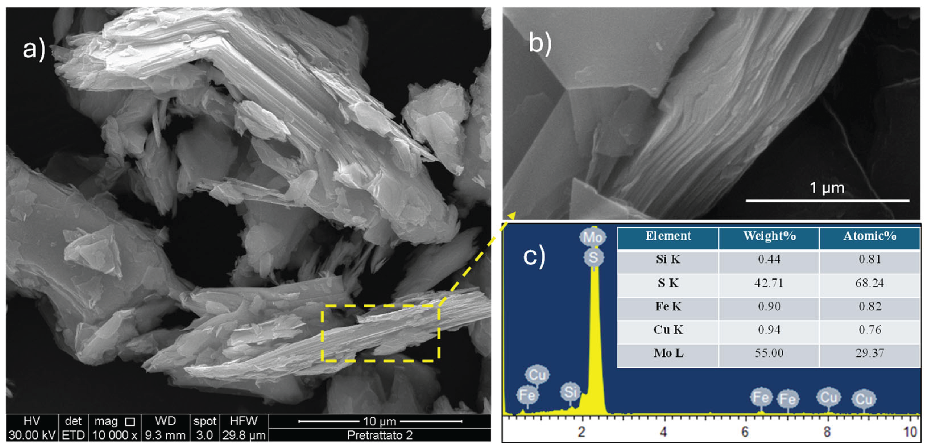
Figure 2.
Concentrated and diluted MoS2 colloidal suspensions in acetonitrile (a); and aluminum slotted specimen stub with a glass slide coated by MoS2 (b).
Figure 2.
Concentrated and diluted MoS2 colloidal suspensions in acetonitrile (a); and aluminum slotted specimen stub with a glass slide coated by MoS2 (b).
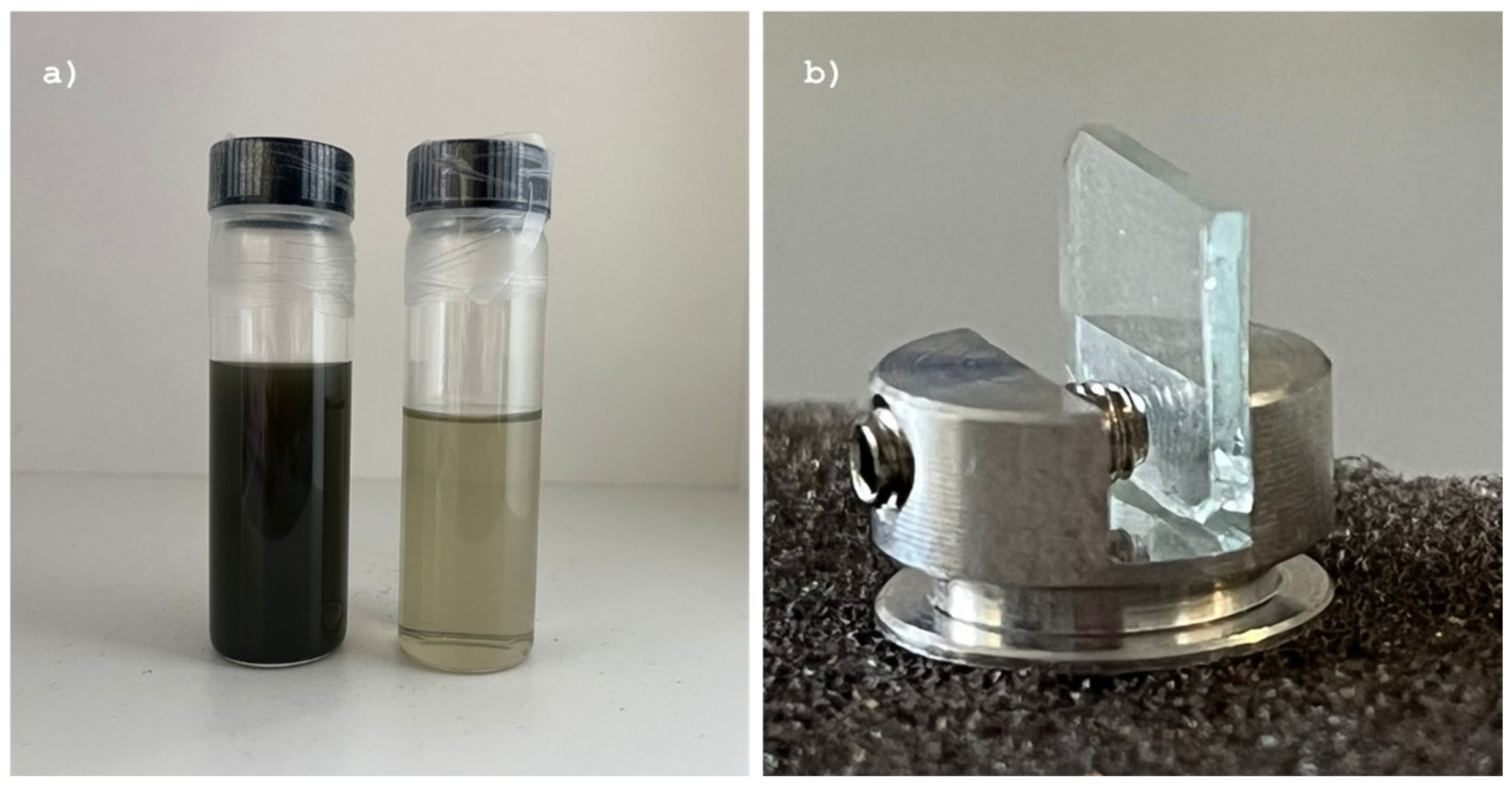
Figure 3.
UV-Vis spectrum of MoS2 colloidal suspension (a) and schematic representation of the electronic band structure of MoS₂ at the K point, highlighting the transitions between the valence and conduction bands that give rise to the A and B absorption features observed in the spectrum. This simplified diagram emphasizes the electronic origin of transitions (b).
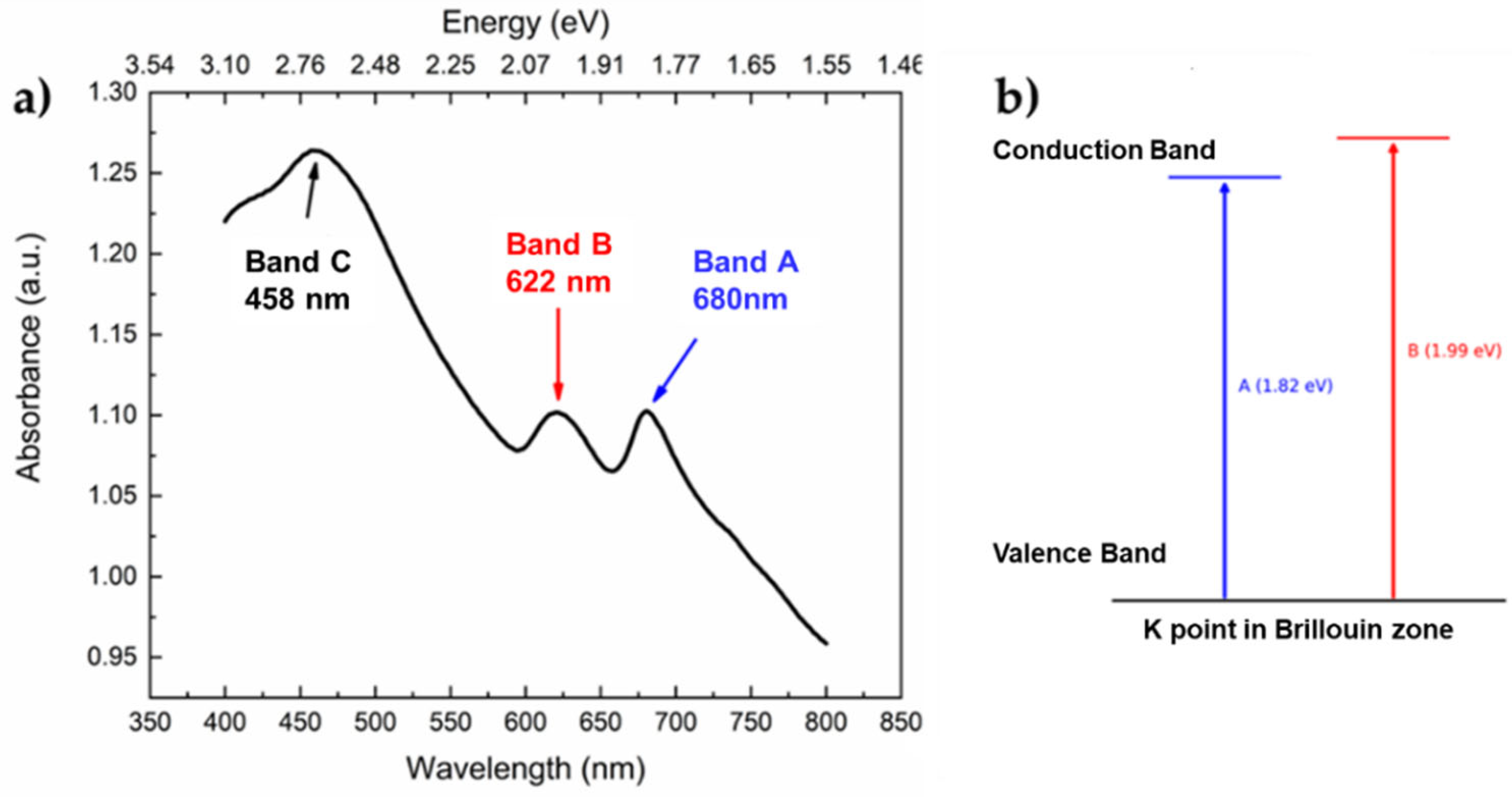
Figure 4.
Modified Tauc plot of the MoS2 colloidal suspension.
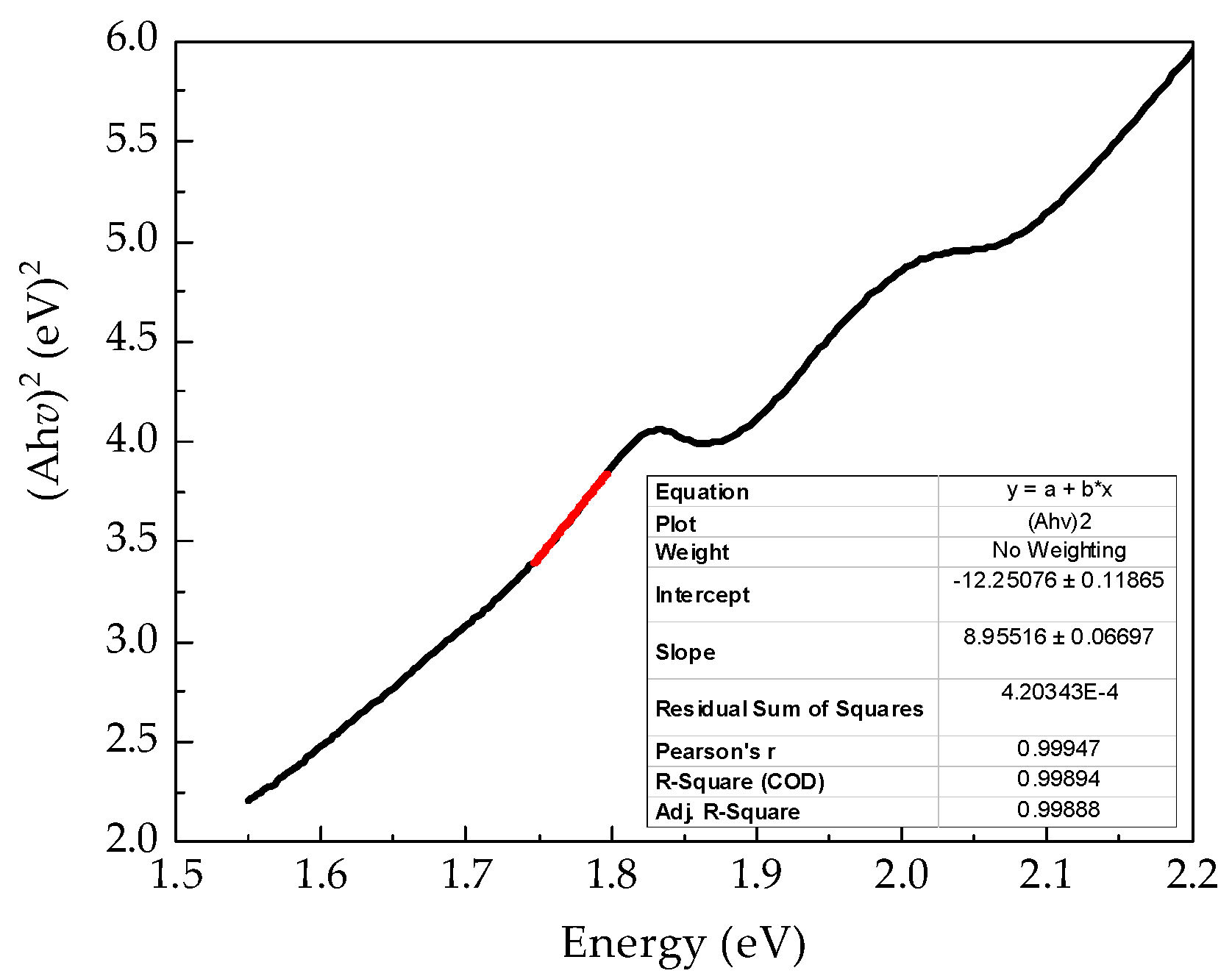
Figure 5.
Schematic representation of different sample positioning and related SEM micrographs: standard sample positioning (a,b) and ~90°-tilting (c,d).
Figure 5.
Schematic representation of different sample positioning and related SEM micrographs: standard sample positioning (a,b) and ~90°-tilting (c,d).
Disclaimer/Publisher’s Note: The statements, opinions and data contained in all publications are solely those of the individual author(s) and contributor(s) and not of MDPI and/or the editor(s). MDPI and/or the editor(s) disclaim responsibility for any injury to people or property resulting from any ideas, methods, instructions or products referred to in the content. |
© 2025 by the authors. Licensee MDPI, Basel, Switzerland. This article is an open access article distributed under the terms and conditions of the Creative Commons Attribution (CC BY) license (http://creativecommons.org/licenses/by/4.0/).
Copyright: This open access article is published under a Creative Commons CC BY 4.0 license, which permit the free download, distribution, and reuse, provided that the author and preprint are cited in any reuse.


