
Submitted:
31 October 2025
Posted:
03 November 2025
You are already at the latest version
Abstract
The growing interest in high-power amplifier for the terahertz (THz) Rader system leads to significant performance improvements of THz wave traveling-wave tubes (TWT). This article presents a detailed development of a G-band pulsed wave TWT with 120·W output power. Three approaches have been combined to improve the tube’s output power including proposing the modified folded waveguide (MFWG) slow wave structure (SWS), using large beam current, and adopting phase velocity tapering (PVT). Firstly, the MFWG SWS circuit has additional degree of freedom that can be used to achieve approximately 36% higher interaction impedance than that in the conventional folded waveguide (CFWG). Subsequently, the electron beam current was increased to approximately 100 mA to boost the DC power of the electron beam. Finally, the PVT technology dramatically enhanced the output power from 98 W to 143 W, concomitant with a notable increase in electronic efficiency from 4.75% to 7.03%. Hot experimental results show that the measured output power can be over 100 W at 20% duty cycle within a bandwidth of 5 GHz when the operation voltage and the current are 22.48kV and 103.5 mA, respectively. Besides, the maximum power is 121 W with the corresponding electronic efficiency of 5.1%. The proposed G-band 100 W TWT will have broad applications in far-distance high-resolution imaging.
Keywords:
G-band
; traveling wave tube
; hybrid folded waveguide
; phase velocity tapering
1. Introduction
Terahertz waves exhibit excellent penetration capability and high-resolution characteristics, providing new potential for synthetic aperture radar (SAR) applications. Their short wavelength enables high azimuth resolution even with relatively small antennas and apertures making SAR systems suitable for platforms with strict size and weight constraints while maintaining high frame rates. Additionally, the large bandwidth supports finely detailed range resolution. Video synthetic aperture radar (ViSAR) further enhances the ability to monitor and track dynamic targets in complex environments by generating time-continuous radar image sequences [1,2,3,4].
However, terahertz waves experience significantly higher atmospheric attenuation compared to microwaves, which generally restricts operation to specific transmission windows—such as the atmospheric window centered around 220 GHz in G-band. As a key component of terahertz ViSAR systems, the G-band traveling wave tube (TWT) amplifier plays a critical role in determining the overall technical performance and tactical capabilities of the radar system [5].
Therefore, improving the peak and average power of TWTs is the core issue in radar applications. As the operating frequency increases to the terahertz region, FWG, with its advantages of simple structure and large power capacity, is the best choice for THz TWTs, and has been widely studied by researchers both theoretically and experimentally. Northrop Grumman has made significant progress in FWG-TWT devices at 0.22 THz. The device can product output power greater than 50 W with in a bandwidth of 2.4 GHz [6]. Electron Devices Division of L3 Technology presented a tube of which the output power exceeds 20 W with the same bandwidth [7]. Beijing Vacuum Electronics Research Institute (BVERI), located in Beijing, China, has recently developed a family of TWTs operating in G band. In 2021, BVERI announced a pulsed G-band 50W TWT designed for radar systems [8]. More recently, in 2024, we demonstrated advances of a high efficiency 30-W G-Band Continuous Wave TWT [9]. In 2025 a 60W TWT operating with a 40% duty cycle was reported for use in THz radar applications [10]
Although the performance of TWTs has been greatly improved, power remains a key factor limiting the tactical indicators of the radar system. As established, the output power Po is related to the beam power Pbeam by the electron efficiency ηe according to the equation:
Po =ηe ×Pbeam =ηe × Uk × Ik.
where Uk and Ik represent the cathode voltage and current, respectively.
To achieve higher power, our work focused on increasing ηe and Ik. Therefore, the device was developed following the design methodology outlined below.
(1) The MFWG has been proposed to increase higher interaction impedance and ηe.
(2) A large beam current Ik is used to significantly increase DC power
(3) The phase velocity tapering technique was utilized to significantly enhance output power.
Through the aforementioned methodology, the development of a 100 W G-band TWT was systematically pursued, encompassing stages of analysis, design, fabrication, assembly, and hot testing. The prototype tube was tested under 20% duty cycle with a beam current of 103.5 mA and voltage of 22.48 kV. The saturation output power measured is over 100 W with 5 GHz bandwidth and the maximum power is 121 W with the corresponding electronic efficiency of 5.1%.
2. Proposal and Characteristics of the MFWG
2.1. MFWG SWS Evolving From CFWG SWS
Figure 1(a) is the vacuum model of CFWG. Figure 1 (b) and (c) are the front view and left side view respectively. The geometric parameters are defined as follows: “a” denotes the broadside length, “b” the narrow-side width, “p” the half-period, “r” the electron beam tunnel radius, and “h” the height of the straight section. The centers of the inner and outer arcs coincide and are located at the same position at the end of the straight waveguide as shown in Figure 1(b). Besides, the width of the narrow side stays constant throughout the circuit as illustrated in Figure 1 (b) and (c).
Figure 1(d) is the vacuum model of MFWG. Figure 1 (b) and (c) are the front view and left side view respectively. The centers of the inner and outer arcs no longer coincide but are determined by the heights of the inner and outer sides of the straight waveguide, respectively. The vertical distances between the centers and beam tunel for both the inner and outer bends are defined as “h1” and “h2”. The width of the narrow side no longer stays constant and the maximum width is “bf” as shown in Figure 1 (b) and (c).
As illustrated in Figure 1, the MFWG has additional degree of freedom that can be used to achieve higher interaction impedance in the CFWG. The structural difference results in significant improvements.
2.2. High Frequency Characteristics of the MFWG
The SWS, where beam–wave interaction is performed, largely determines the performance of the TWT, such as output power, bandwidth, gain, operating voltage. The high frequency characteristics include the dispersion relation and interaction impedance. Both indicators are analyzed using the Eigenmode Solver in CST Microwave Studio (MWS) [11], applied to a single unit cell of the SWS with periodic boundary conditions along the axial direction. By imposing a fixed periodic phase shift, the corresponding resonant frequency is obtained. The phase velocity is then derived from the relationship between the resonant frequency and the phase shift per period using the expression:
where f denotes the resonant frequency, p the length of one period, and θ the phase shift per period.
vp = 2πfp/θ,
The interaction impedance, which quantifies the coupling strength between the electron beam and the high-frequency electromagnetic field, is evaluated numerically based on its established definition. For the mth spatial harmonic, the interaction impedance is defined as follows:
The power carried by the TE₁₀ mode in the waveguide corresponds to Wrf. This value is obtained in CST MWS by integrating the Poynting vector over the entire cross-sectional area of the waveguide using the post-processing tools. Meanwhile, the amplitude Em of the mth spatial harmonic along the axis is computed via Fourier decomposition applied to the on-axis electric field distribution. Based on these computed quantities, a custom post-processing script is implemented to automatically evaluate the interaction impedance according to its definition.
A parametric study was conducted to comprehensively evaluate the performance l of the MFWG by varying the center positions of the inner and outer arcs. The results, presented in Figure 2, demonstrate that reducing the height “h1” significantly enhances the interaction impedance. Specifically, the value at the center frequency increases by 25%, from 2.5 ohms to 3 ohms. Concurrently, the normalized phase velocity rises from 0.280 to 0.284, resulting in an increase in the operating voltage from 21.29 kV to 21.94 kV.
Figure 3 shows influence of “h2”on cold characteristics. As the height of h2 increases, the variation of interaction impedance within the frequency band becomes more complex. Specifically, at the lower end of the band, the interaction impedance increases markedly—from 3.65 ohms to 4.0 ohms, representing a rise of approximately 10%—while its growth remains more gradual at higher frequencies. Concurrently, the normalized phase velocity decreases continuously from 0.280 to 0.272, and the corresponding operating voltage decreases from 21.29 kV to 20.02 kV. This is attractive to designers as the reduction in operating voltage is accompanied by a concurrent improvement in interaction impedance.
Figure 4 shows influence of simultaneous variation of structural parameters “h₁” and “h₂” on cold characteristics. When the height of “h2” increases while the height of “h1” decreases, the interaction impedance significantly increases throughout the entire frequency band. Specifically, at the lower end of the frequency band, the interaction impedance increased from 3.7 to 5.2 ohms, an increase of 40.5%. The interaction impedance at center frequency increased from 2.5 to 3.4 ohms, a 36% increase. The interaction impedance of the high-frequency end has increased from 1.8 to 2.4 ohms, an increase of 33.3%. The coincidence of normalized phase velocity curves means that there has been no change in operating voltage and bandwidth. This indicates that the combination of “h1” and “h2” can achieve a larger interaction impedance without increasing the operating voltage or sacrificing the operating bandwidth.
Building on the key performance metrics outlined above,the MFWG demonstrates superior output power capacity compared to the FWG, making it a more promising candidate for high-power device applications.
3. Generation and Focusing of the large Electron Beam Current
The use of a high-power electron beam can significantly enhance the output power of the G-band traveling-wave tube (TWT). Here, the beam current was successfully boosted to over 100 mA. This deliberate increase in current directly resulted in a proportional and substantial enhancement of the electron beam DC power, providing a much more robust foundation for efficient energy extraction. In accordance with the design specifications, the operating voltage and current have been set to 22 kV and 102 mA, respectively. However, designing a new optical system for operation in G band is never an easy task. Figure 5 shows the simulation model of electron gun and PPM system. The Pierce electron gun adopts an M-type cathode with a 10 A/cm2 load to generate 100 mA beam current. A pencil electron beam was formed and the current density was compressed to over 880 A/cm² using a focus electrode and an anode. The periodic permanent magnet (PPM) focusing system employs samarium-cobalt magnets and iron pole pieces. The period and outer diameter is 7.2 mm and 10mm, respectively. As shown in Figure 6, the on-axis Bz of peak value calculated using a CST 3D particle magnetic field solver is 0.72T. Simulations performed using the CST 3D particle tracking code confirm that the electron optical system successfully generates and propagates a 22 kV, 100 mA pencil beam with an average radius of 0.06 mm through a 0.12 mm-radius beam tunnel spanning 70 mm in length. The achieved beam transmission ratio was 100% in simulation.
4. Adopting the Phase Velocity Tapering Technique
The principle of a TWT is the interaction between an electron beam and radio frequency (RF) waves propagating along a slow wave structure. Under DC voltage acceleration, the speed of the electron beam is slightly higher than the phase velocity of the RF wave. During the interaction process, the electron beam continuously transfers its kinetic energy to the RF wave, amplifying it. The amplitude of the RF wave that obtains energy continuously increases, but at the same time, the electron beam also transfers a large amount of kinetic energy to the RF wave, causing its own velocity to slow down. After losing energy, the electron's velocity will gradually lag behind the RF wave, causing the two to lose synchronization. Once out of step, the energy exchange efficiency will sharply decrease, and even electrons will absorb energy from RF waves in reverse, limiting the output power and efficiency of the TWT. The phase velocity tapering (PVT) technique is a dynamic matching technique that dynamically adjusts the speed of microwave waves during amplification by changing the physical size of the SWS, so that it maintains the best synchronization state with the electron beam. The PVT technique has been widely used to improve the electronic efficiency [8,9,10].
In our design, the primary goal of circuit optimization is to maximize electronic efficiency. In addition, the PVT design must be effective within the required frequency bandwidth. Finally, the designed structure must be able to be precisely manufactured using existing processes. The structural parameter “p” is used to adjust the phase velocity. Figure 7 shows the circuit with the taper.
Figure 8(a) illustrates the output power of the MFWG TWT without and with the taper calculated by Microwave Tube Simulator Suite [12]. It is evident that the incorporation of a tapered section in the tube leads to a substantial improvement in output power across the entire operating frequency band. At 0.215 THz, the use of this taper enhances the output power from 98 W to 143 W and raises the electronic efficiency from 4.75% to 7.03%.
Figure 8(b) depicts the output power variation with circuit length for two circuits. Notably, MFWG TWT achieved twice energy exchanging.
5. Fabrication, Assembling and Hot Test
The high frequency circuit for the TWT is divided into two parts and fabricated using Nano computer numerical control (CNC) milling. Statistical analysis of the measurement results shows that the machining accuracy of the MFWG SWS is better than ±2 µm. During the high-frequency circuit machining process, the metal surface roughness is reduced through repeated micro-milling, resulting in a measured roughness of approximately 60 nm.
In addition to the electron optical system and high-frequency system developed in this article, the diamond window reported in the literature [9] were also used here.
After debugging, the transmission rate reaches 93%. No oscillation is detected
A schematic of the experimental setup is presented in Figure 9. The input power to the TWT is supplied by a solid-state amplifier-multiplier chain (AMC). Two directional couplers are employed to sample the input and output power levels, which are simultaneously measured using two independent THz power meters. The TWT operates in pulsed mode under optimized conditions at 22.48 kV and 103.5 mA. Thermal management is achieved through conduction cooling via the mounting plate.
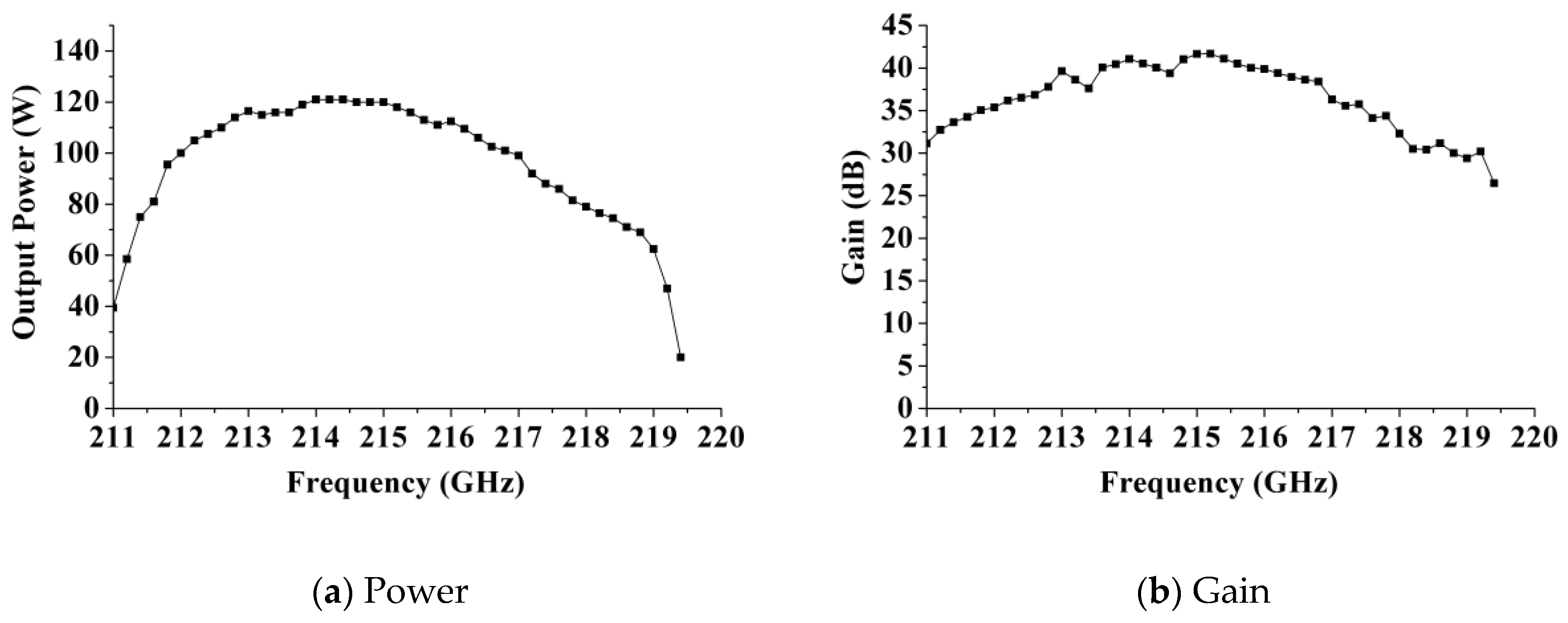
The measured saturation output power is shown in Figure 10 (a). The maximum power is 121W at 215GHz. The saturation output power is over 100 W in 212-217 GHz. The measured saturation gain is shown in Figure 10(b). The maximum gain is 41dB. The ripples of the gain are mainly caused by the reflections of the directional couplers and the waveguide joints.
6. Conclusions
This article proposes a modified folded waveguide (MFWG) and cold characteristics are analyzed and contrasted. Then,a 100 W pulsed traveling wave tube has been designed and developed based on this SWS. Owing to phase velocity tapper and higher beam current,the simulated output power has been promoted to 142W. Hot experimental results show that the measured output power can be over 100 W at 10% duty cycle within a bandwidth of 5 GHz when the operation voltage and the current are 22.48kV and 103.5 mA, respectively. And, the maximum power is 121 W with the corresponding electronic efficiency of 5.1%. The overall weight of the TWT is less than 1.9 kg. The proposed G-band 100 W TWT will have broad applications in far-distance high-resolution imaging.
Author Contributions
Design and simulation, X.B.; debugging and measuring, X.B, Y.D.; machining, X.X.; technical support, L.Z, P.P, J.C, J.F. All authors have read and agreed to the published version of the manuscript.
Funding
This research received no external funding.
Data Availability Statement
Not applicable.
Conflicts of Interest
The authors declare no conflicts of interest.
References
- Zhang, X.; Shkurinov, A.; Zhang, Y. Extreme terahertz science. Nature Photon. 2017,11,16–18. [CrossRef]
- Armstrong, C.M. The truth about terahertz. IEEE Spectr. 2012, 49, 36–41. [CrossRef]
- Wang, W.; An, D.; Zhou, Z. Preliminary Results of Airborne Video Synthetic Aperture Radar in THz Band. 6th Asia-Pacific Conference on Synthetic Aperture Radar (APSAR), Xiamen, China, 2019, pp. 1-4.
- Wu, F.; Li., S.; Lin, J. Study of Airborne THz ViSAR. 46th International Conference on Infrared, Millimeter and Terahertz Waves (IRMMW-THz), Chengdu, China, 2021, pp. 1-2.
- Kim, S.; Fan, R.; Dominski, F. ViSAR: A 235 GHz radar for airborne applications. IEEE Radar Conference, Oklahoma City, OK, 2018, pp. 1549-1554.
- Basten, M.; Tucek, J.; Gallagher, D.; Kreischer, K. 233 GHz high power amplifier development at Northrop Grumman. In Proceedings of the 2016 IEEE International Vacuum Electronics Conference (IVEC), Monterey, CA, USA, 2016; pp. 1–2.
- Armstrong, C.M.; Kowalczyk, R.; Zubyk, A.; Berg, K.; Meadows, C.; Chan, D.; Schoemehl, T.; Duggal, R.; Hinch, N.; True, R.B.; et al. A Compact Extremely High Frequency MPM Power Amplifier. IEEE Trans. Electron Devices. 2018, 65, 2183–2188. [CrossRef]
- Bian, X.; Pan, P.; Tang, Y.; Lu, Q.; Li, Y.; Zhang, L.; Cai, J.; Feng, J. Demonstration of a Pulsed G-Band 50-W Traveling Wave Tube. IEEE Electron Device Lett. 2020, 42, 248–251. [CrossRef]
- Bian, X.; Pan, P.; Du, X.; Song, B.; Zhang, L.; Wu, X.; Cai, J.; Feng, J. Demonstration of a High Efficiency and Wide Band 30-W G-Band Continuous Wave Traveling Wave Tube. IEEE Electron Device Lett.2024, 45, 1969–1972. [CrossRef]
- Bian, X.; Pan, P.; Du, X.; Feng, Y.; Li, Y.; Cai, J.; Feng, J. Design and Experiment of Modified Folded Waveguide Slow Wave Structure for 60-W G-Band Traveling Wave Tube. IEEE Microwave and Wireless Technology Lett., 2025. 35, 1194–1197. [CrossRef]
- CST User Manual. [Online]. Available: http://www.cst.com (accessed on Mar. 2,2024).
- Li, B.; Li, J.; Hu, Q.; Hu, Y.; Xu, L.; Huang, T.; Jin, X.; Zhu, X.; Yang, H. Recent Development to the Microwave Tube Simulator Suite. IEEE Trans. Electron Devices.2014, 61, 1735-1741. [CrossRef]
Figure 1.
Vacuum model and front view and left side view.
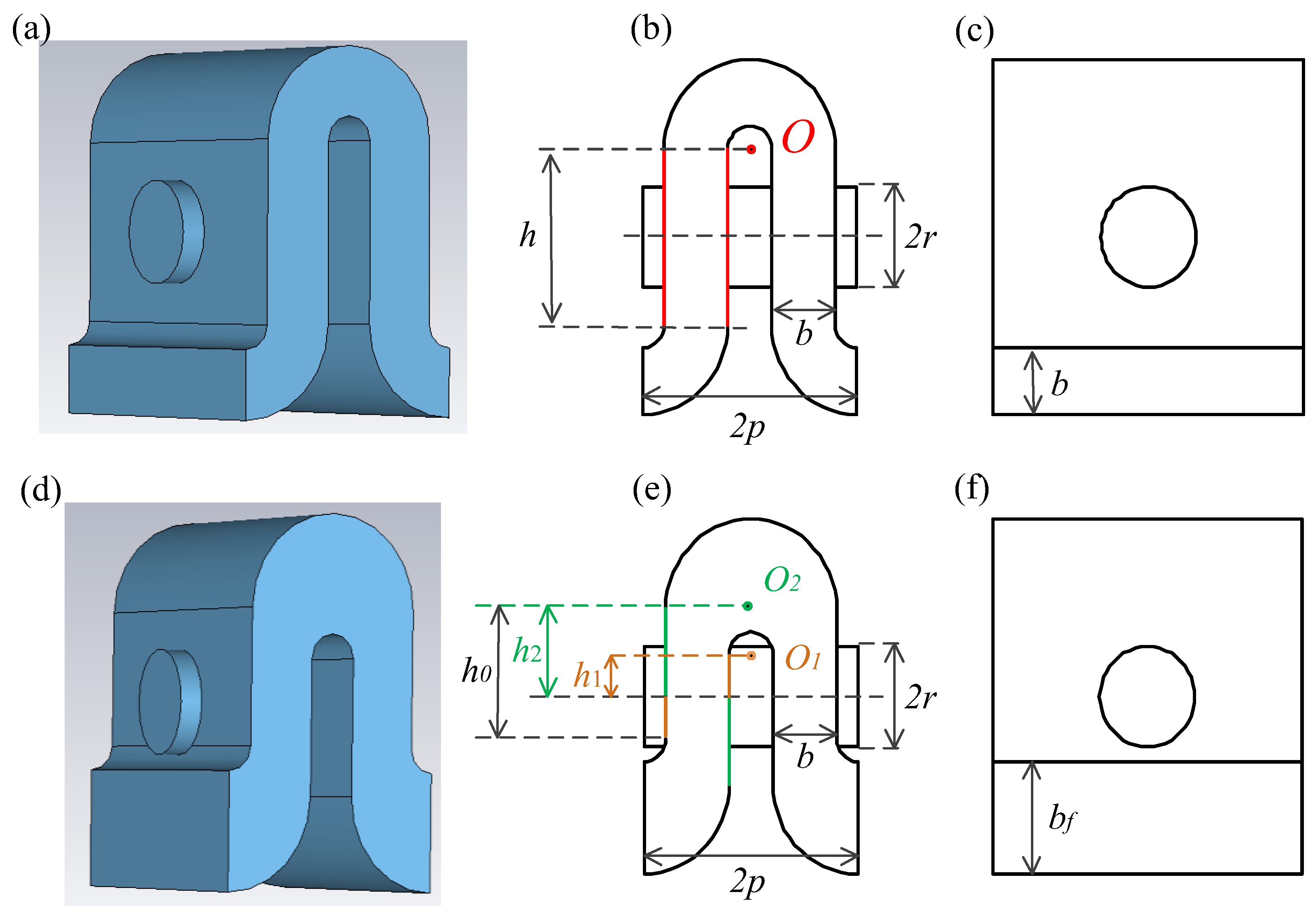
Figure 2.
Influence of “h1” on cold characteristics. (a) Interaction impedance. (b) vp/c.
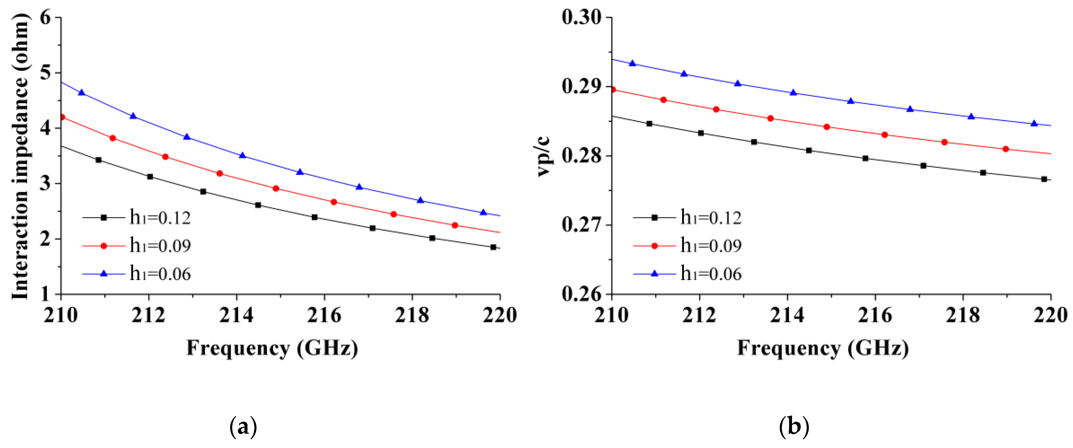
Figure 3.
Influence of “h2” on cold characteristics. (a) Interaction impedance. (b) vp/c.
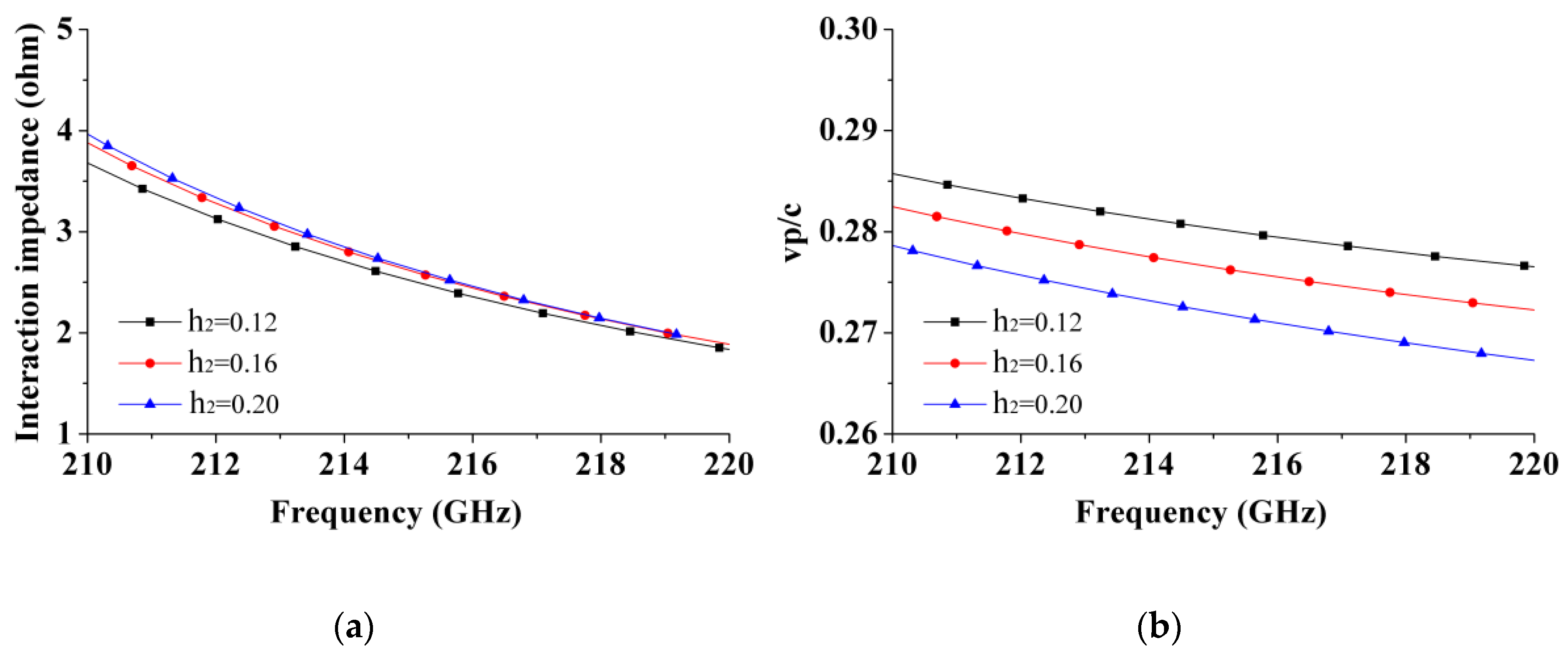
Figure 4.
Influence of simultaneous changes in “h1” and “h2” on cold characteristics. (a) Interaction impedance. (b) vp/c.
Figure 4.
Influence of simultaneous changes in “h1” and “h2” on cold characteristics. (a) Interaction impedance. (b) vp/c.
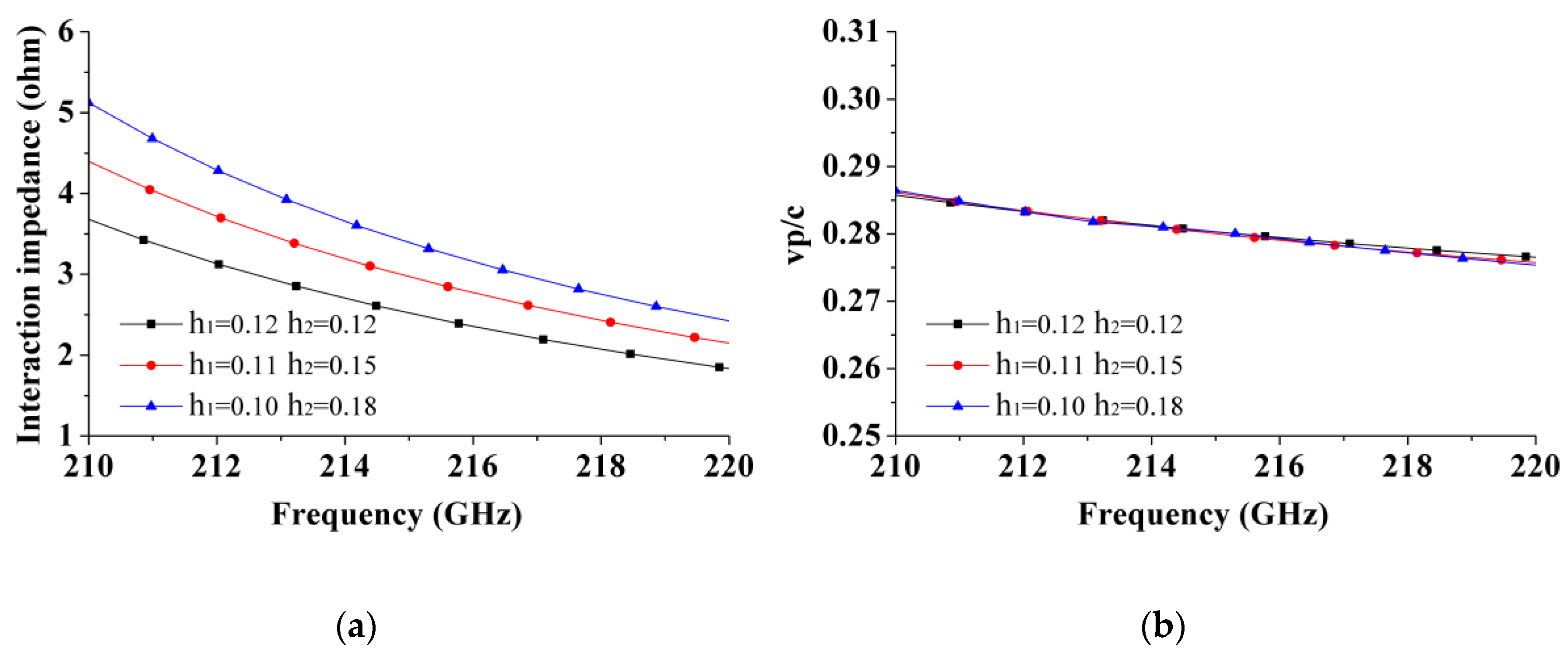
Figure 5.
Simulation model of electron gun and PPM system.
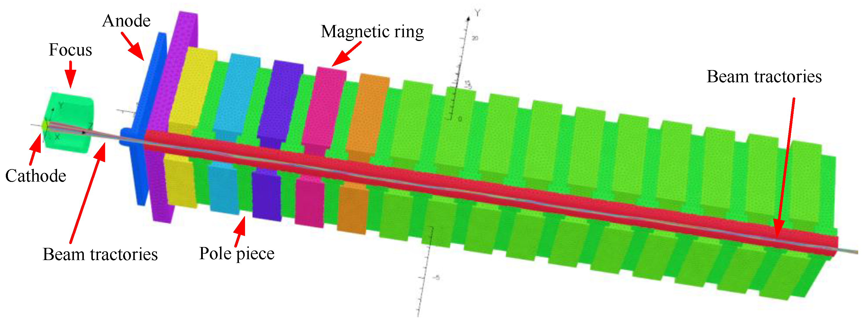
Figure 6.
Simulated longitudinal magnetic field distribution of PPM system and beam trajectories.
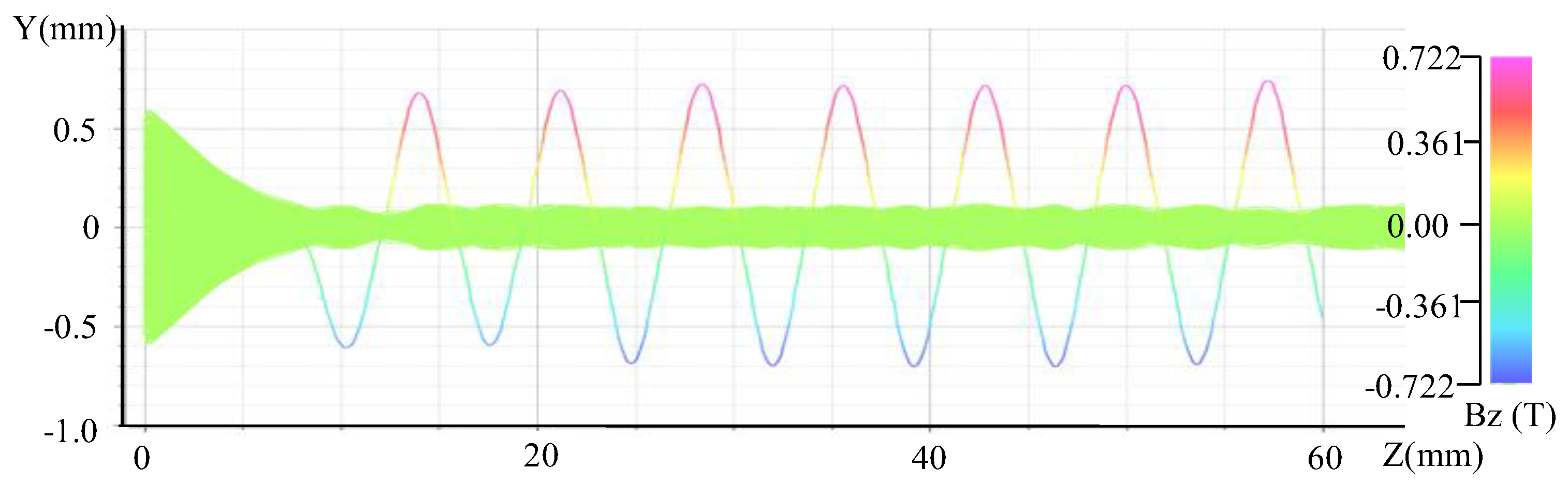
Figure 7.
Circuit diagram.
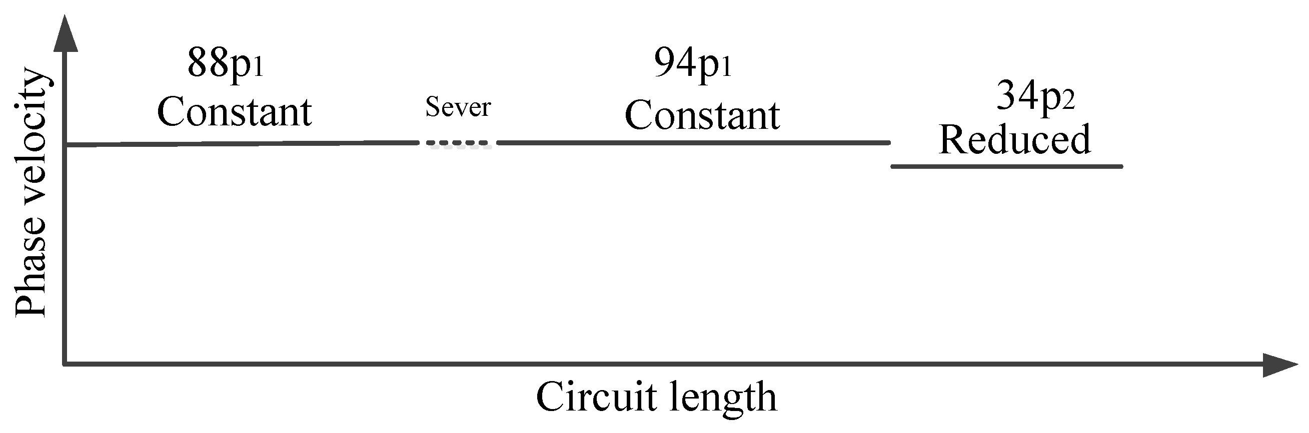
Figure 8.
(a) Output power predicted by MTSS. Power. (b) The growth curve of power along the interaction circuit.
Figure 8.
(a) Output power predicted by MTSS. Power. (b) The growth curve of power along the interaction circuit.
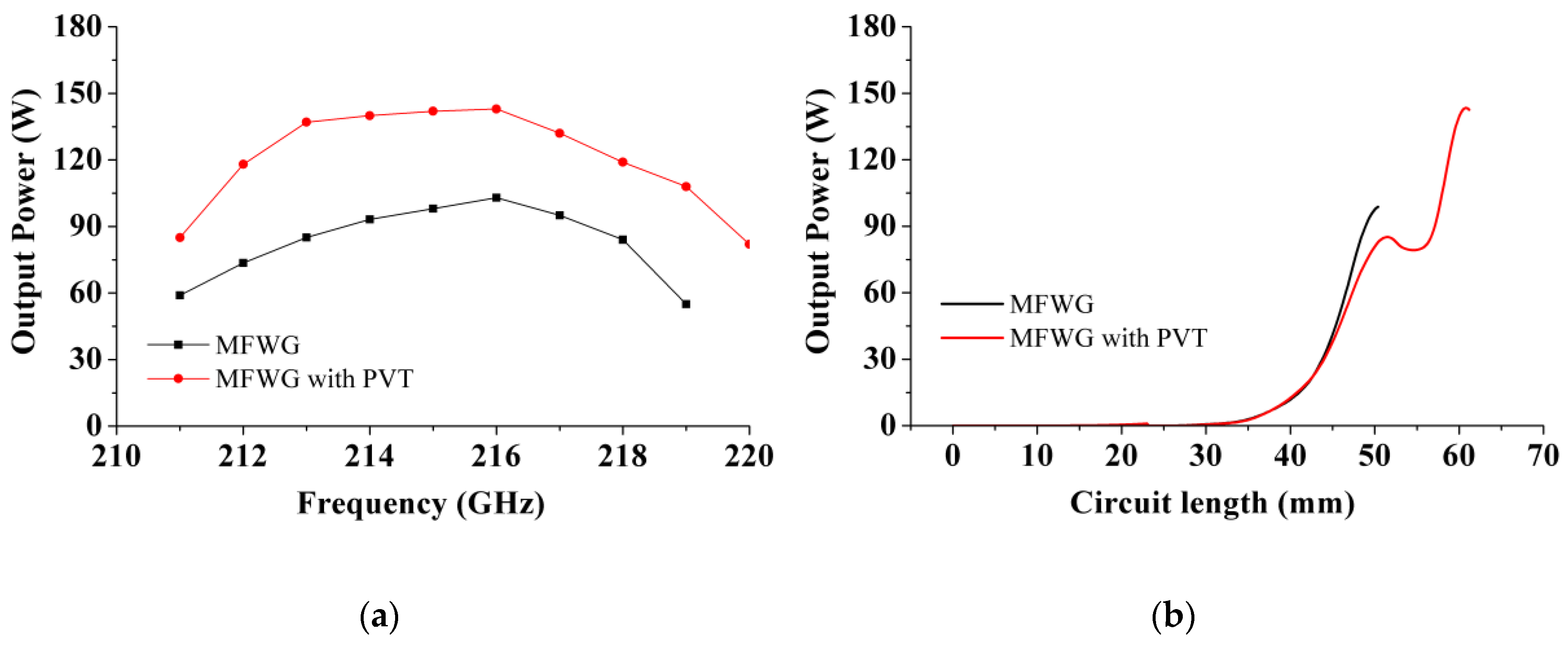
Figure 9.
The protype of tube and block diagram of the experimental setup.
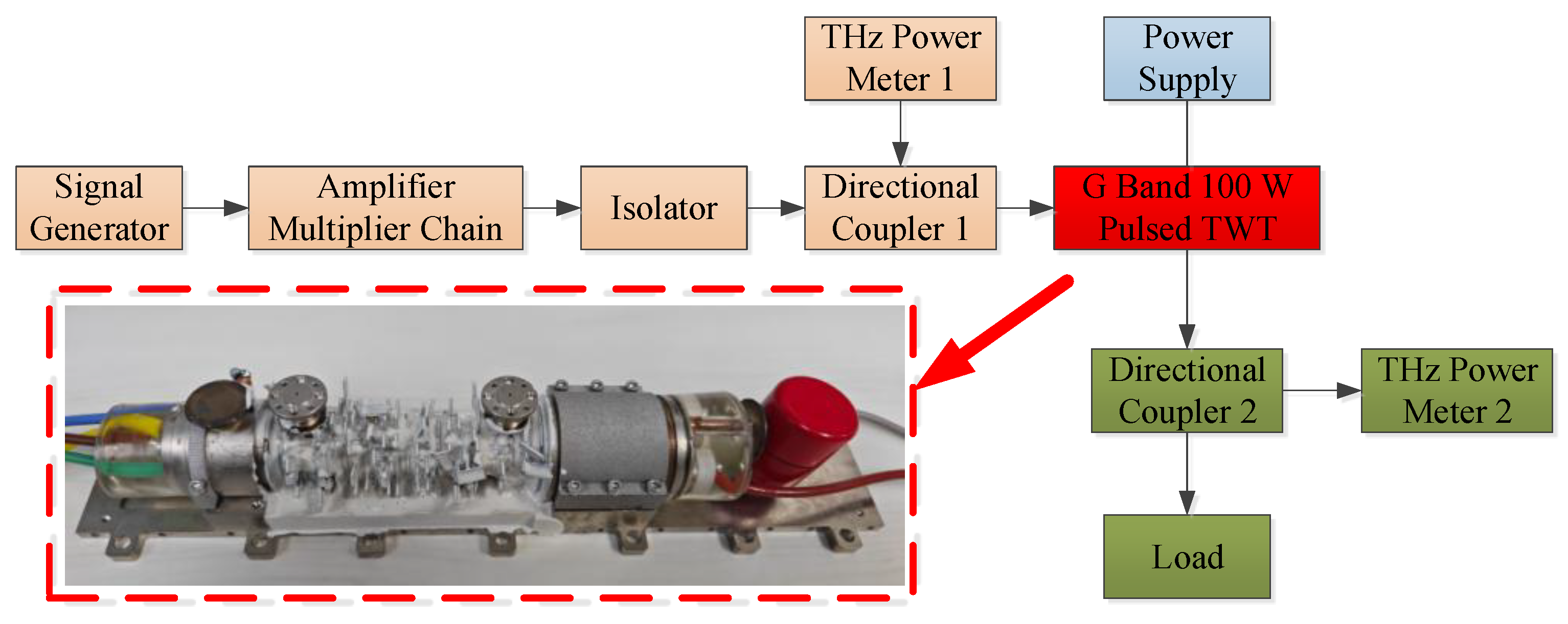
Figure 10.
Hot test results.
Disclaimer/Publisher’s Note: The statements, opinions and data contained in all publications are solely those of the individual author(s) and contributor(s) and not of MDPI and/or the editor(s). MDPI and/or the editor(s) disclaim responsibility for any injury to people or property resulting from any ideas, methods, instructions or products referred to in the content. |
© 2025 by the authors. Licensee MDPI, Basel, Switzerland. This article is an open access article distributed under the terms and conditions of the Creative Commons Attribution (CC BY) license (http://creativecommons.org/licenses/by/4.0/).
Copyright: This open access article is published under a Creative Commons CC BY 4.0 license, which permit the free download, distribution, and reuse, provided that the author and preprint are cited in any reuse.


