Submitted:
16 October 2025
Posted:
16 October 2025
You are already at the latest version
Abstract
A gate driver on array (GOA) circuits employed with amorphous indium-gallium-zinc oxide (IGZO) based thin film transistors (TFTs) have been successfully utilized to generate the driving signals for the commercialization of active matrix organic light-emitting diode (AMOLED) displays. The depletion-mode TFTs in GOA circuits can be completely turned off by the introduction of series-connected two-transistor and dual low voltage level power signals. Simulation results demonstrate that GOA exhibits high process stability with threshold voltage margin from -5V to +5V. Furthermore, GOA output characterization and mobility compensation effect are evaluated by the integration of GOA and pixel in a 31-inch 4K AMOLED display. Experimental results demonstrate that full swing driving pulses can be obtained by GOA. Finally, the stripe mura in display caused by mobility variation can be successfully eliminated by the introduction of GOA circuits.
Keywords:
AMOLED
; GOA
; IGZO-TFTs
; process stability
1. Introduction
Along with the rapid development of lightness and wearability in displays, active-matrix organic light-emitting diode (AMOLED) has become an emerging technology potentially capable of small volume and weight, fast response and wide color gamut [1,2,3,4]. Meanwhile, since the technology is highly compatible with ink-jet printing process, growing number of flat panel display manufacturers have proposed AMOLED roadmap [5]. Nevertheless, manufacturing cost has been the major challenge to the commercialization of AMOLED display, and therefore the utilization of AMOLED displays is limited to the premium consumer electronic market in worldwide [6]. A strong demand for thin film transistors (TFTs)-compatible, hybrid integrated circuit system with low cost and simplified manufacturing process has arisen. In this system, direct fabrication method of gate driver on array (GOA) circuit enabled by TFT process is utilized to generate gate-pulse signals instead of external gate driving chips and the related gate chip bonding process can be simplified [7,8].
Two well established TFT techniques have been explored to fabricate AMOLED backplane, i.e., low temperature poly-Si (LTPS) [9,10] and amorphous indium-gallium-zinc oxide (IGZO) [11,12]. LTPS TFTs present well-performed electrical properties that are characterized by their high mobility (~100cm2/V.s) and good high-temperature reliability (stable at temperature of 60°C), while complex process using an excimer laser annealing (ELA) treatment is required to improve the crystalline effect in poly-Si films [13]. The poorness of crystalline uniformity in Si films during ELA process and high ELA equipment cost limits the use of LTPS TFTs in high generation display manufacture line [14,15]. Recently developed IGZO films as channel materials in active layer demonstrates high uniformity over large scale [16,17]. Especially, IGZO-TFTs have been achieved in commercial application of AMOLED displays in the mainstream generation 8.5 line (glass size=2200mm×2500mm) [18].
The successful use of IGZO-TFTs to AMOLED displays has motivated investigations into the research of GOA with IGZO-TFTs, particularly circuit topology design with depletion-mode TFTs [19,20]. It should be noted that, recent work performed by LG’s researchers implies that IGZO-TFTs exhibit poor temperature reliability [21,22]. In their research, when displays are turned on, the transformation of operation temperature in displays causes brightness mura, rendering image quality sensitive to variations of mobility in TFTs. To enable the adoption of IGZO-TFTs in AMOLED display, pixel design with mobility compensation function has to be introduced to eliminate brightness mura across the display and it is necessary for IGZO-GOA to export high speed shift register signals, as well as driving pulses for mobility compensation function. However, AMOLED displays with GOA technology has not yet entered mass production phase, because most researches in IGZO-GOA focus on conventional shift register programing mode [23,24,25].
In this work, we demonstrated an external mobility compensation system for AMOLED displays, in which a IGZO-TFT based GOA circuit has been utilized to export shift register signals and external mobility compensation signals simultaneously. Subsequently, the mechanisms of external compensation technology and GOA topology were systematically investigated. Furthermore, the performance and reliability of GOA were evaluated by integrating GOA to a 31-inch 4K AMOLED display. Finally, mobility compensation procedure was performed to improve the image quality.
2. The Mechanism of the External Compensation System
The ability to detect mobility information of driving TFTs in pixels is fundamental for the commercialization of AMOLED displays based on IGZO-TFT technology. In order to maintain high picture quality, an external compensation system, shown in Figure 1, has been utilized to avoid the influence of mobility to luminance over the whole display. In this structure, a basic pixel cyclic unit is composed of three sub-pixels (R/G/B). According to display resolution (2160*3840, 4K), individual pixel is repeatedly expanded toward the horizontal and vertical direction, respectively. Accurate placement of sixteen source chips at the bottom side supplies significant display signals for this system. Each source chip is capable of supporting 720 data signals and 720 sense signals, corresponding to the number of data and sense lines in 2160*240 pixels. The overall data signals are timing-controlled and image-processed by two separate time-controller board, which is synchronized each other so that no image discrepancy occurs between left and right side of display. Meanwhile, GOA circuits are arranged symmetrically on both sides to provide driving signals for pixels.
The schematic of external compensation system can be seen in Figure 2a, each pixel circuit is composed of two switching TFTs (T2, T3), a driving TFT (T1) and a storage capacitor (Cst). Two scan signals (WR, RD), generated by GOA, are used to supply switching signals. Simultaneously, data voltage is utilized to control the gray scale in pixels. Furthermore, a high constant voltage (VDD, 24V) and a low constant voltage (VSS, 0V) are used to control the drain electrode voltage of T1 and cathode voltage of OLED. The establishment of 3T1C circuit ensures that the mobility message of T1 can be detected by an external sense system. In this system, the anode of OLED, referred to S in circuit, connects to source chip through metallic sense lines on glass. Each of the Spre and Sam switches alternatively performed a turn-on operation and a turn-off operation in source chips. Reference source (Vref, 1V) and analog-to-digital converter (ADC) are applied to reset the voltage in S and transfer voltage message to digital signal, respectively.
Figure 2b shows the time diagram of individual pixel at the emission stage. The operation can be divided into two stage. At first, WR and RD are simultaneously switched to a high voltage. Along with T2 and T3 are turned on, the data voltage (Vdata0, 1~5V) and Vref are separately written to the gate electrode and source electrode of T1. T1 works in the saturation regime, because the Vds (VDD-Vref) voltage is profoundly higher than Vgs-Vth (Vdata0-Vref-Vth) voltage, in which Vth represents the threshold voltage. The drain current of T1 is expressed as
Where W is the channel width, L is the channel length, Cox is the insulation capacitance between active layer and gate electrode. μ is the initial mobility. At this time, the lower voltage of Vref (1V) than the threshold voltage of OLED (2.5V) ensures OLED is compeletely turned off. Secondly, when WR and RD are discharged to a low voltage, T2 and T3 are switched off. Simultaneously, the voltages of G and S are coupled interactively to high voltage until OLED is turned on. Theoretically, the current penetrated through OLED is kept in accordance with I in equation (1). Since display starts to work, the operation temperature increases significantly and the drain current begins to deviate from the raw data in system. It is necessary to perform mobility compensation operation during display time.
Figure 2c indicates the mechanism of mobility compensation process, which is divided into five stages: In the first stage, RD and Spre are switched to high voltage. OLED device is turned off, since the voltage of S is reset to a low voltage Vref. In the next stage, T2 is turned on by switching WR from low voltage to high voltage. The voltage of G is written to a fixed data (Vdata_sense). The current flowing through T1 can be expressed as follows:
Δμ represents the variety of mobility. In the third stage, WR and Spre are switched to low voltage, and then the current flows toward external source chips through T3. The equation (3) shows the electron transfer process at this time.
t is the charging time, Csense is the parasitic capacitance of sense line. The voltage in S (Vs) recorded at the end of this stage can be detected using external sensing unit. Obviously, the relationship between Vs and mobility (µ+Δµ) can be established. Before display is turned on, the initial drain current Ids0 can be expressed as follow
Assuming mobility has been well compensated (Ids0=Ids1), it is easy to calculate mobility message based on equation (2)~(5).
It can be easily seen that the mobility (μ+Δμ) can be characterized through the variation of voltage in S. In the fourth step, Sam is switched on, and then Vs transfers from analog signal to digital signal by ADC. In the final step, T2 and Spre are turned on and a new data signal is written to pixel (data1). In order to obtain the same current in equation (1), Vdata1 can be calculated in the following equation.
According the equations (6) and (7), Vdata1 is shown in equation (8)
The time diagram of convenient GOA can be seen in Figure 3a. Shift register pulses, separated by blank time at the end of each frame, transport to display area row by row [26,27]. As shown in Figure 3b, in contrast to convenient shift register timing, the important point of this study is the introduction of driving pulses at blank time, because procedure of program stage can’t be disturbed by the operation of mobility compensation. A significant charge time is expected to maximize charging ratio in pixels [28]. As a result, it is necessary to minimize the blank time, because the blank time partially determines the active charging time for each row. In this display, the active charge time (1.85µs) has been identified for individual pixel by reducing blank time to 170µs.
3. GOA Circuit Schematic and Operation
Recent research performed by B. Kim, et al. indicates that IGZO-TFTs often act as depletion mode device [29]. The direct utilization of traditional GOA circuit may cause malfunction of circuit. Series-connected two-transistor (STT) structure has shown the potential to reduce the leakage in TFTs by introducing a feedback unit in circuit [30]. Meanwhile, dual low voltage level power (VGL) structure is used to reduce leakage current from TFTs, which primarily serves to decrease the gate to source voltage (Vgs). Figure 4 exhibits the schematic and time diagram of proposed GOA circuit, which is composed of a pull-up control (T11, T12) unit, pull-up (T21~T23) unit, pull-down unit (T31~T34, T71~T74), pull-down holding (T41~T410), inverter unit (T51~T58), feedback unit (T6), logical sense unit (T81~T85) and bootstrap capacitor (Cbt1~Cbt4). In this circuit, the use of STT structure is to decrease the leakage current of TFTs connecting to Q. Meanwhile, in order to improve the driving force in scan signals (WR, RD), dual VGL structure is utilized to decrease the leakage current in T41~T44.
Given the importance of the reliability in GOA, an investigation to introduce two group inverter unit and pull-down unit is performed in this study. This is necessary to be able to decrease the positive bias temperature stress (PBTS) effect in the TFTs and improve electric reliability of TFTs [31]. LC1 and LC2 are a group of low-frequency AC signals with opposite voltage phase, while CKa, CKb and CKc are a group of high-frequency AC signals. The operation of the proposed unit can be divided into the following periods:
(1) Program time: In the P1 stage, the carrying signal Cout(n-6) switches from a low voltage to a high voltage. At this time, Q is charged to a high voltage through T11 and T12. Cout(n), WR(n) and RD(n) are set to a low voltage when T21, T22 and T23 are turned on. LC1 is high voltage and the first inverter unit (T51, T53, T55, T57) is utilized to reverse the voltage between QB1 and Q. Simultaneously, QB2 maintains a low voltage and T41~T410 are turned off. LSP is switched to a high voltage, and then T81 and T82 are turned on. Subsequently, M rises to a high voltage. In the P2 stage, Cout(n-6) and LSP are switched to a low voltage, T11, T12, T81 and T82 are turned off, Q and M maintain a high voltage. In the P3 stage, CKa, CKb and CKc are switched to a high voltage. Consequently, in contrast to the voltage in phase P1, Q is bootstrapped to a higher voltage through Cbt1~Cbt3. Cout(n), WR(n) and RD(n) are switched to a high voltage. In the P4 stage, CKa, CKb and CKc are switched to a low voltage. Q is bootstrapped to a high voltage through Cbt1~Cbt3. Cout(n), WR(n) and RD(n) are released to a low voltage. In the P5 stage, Cout(n+6) is changed from a low voltage to a high voltage, T31 and T32 are turned on, Q is released to a low voltage and QB1 rises to a high voltage. At this moment, T42, T44, T46, T47 and T48 are turned on, Q, Cout(n), WR(n) and RD(n) maintain low voltage. In the P6 stage, Cout(n+6) switches to a low voltage, and then T31 and T32 are turned off.
(2) Blank time: In the B1 stage, M maintains a high voltage and Reset1 is changed from a low voltage to a high voltage. Since T84 is turned on, Q is charged to a high voltage (VGH) and QB1 transfer from a high voltage to a low voltage. Meanwhile, Cout(n), WR(n) and RD(n) are set to a low voltage. In the B2 stage, CKc transfers from a low voltage (VGL1) to a high voltage (VGH), due to the existence of Cbt1, Q is theoretical bootstrapped to a high voltage VGH+(VGH-VGL1)Cbt1/(Cbt1+Cbt2+Cbt3), and then RD(n) is charged to a high voltage. In the B3 stage, CKb switches from a low voltage to a high voltage and Q is bootstrapped to VGH+(VGH-VGL1)(Cbt1+Cbt2)/(Cbt1+Cbt2+Cbt3). WR(n) is charged to a high voltage. In the B4 stage, Since CKb changes from VGH to VGL, WR(n) is discharged from VGH to VGL. At this moment, Q is decreased to VGH+(VGH-VGL1)Cbt1/(Cbt1+Cbt2+Cbt3). In the B5 stage, WR(n) is charged to a high voltage due to the transform of a low voltage to a high voltage in CKb. In the B6 stage, CKb and CKc are changed to a low voltage. WR(n) and RD(n) are discharged to VGL. In the B7 stage, LSP and Reset2 change to VGH. Q is discharged to a low voltage through T33 and T34. Simultaneously, QB1 rises to a high voltage and T42, T44, T46, T47, T48 are turned on. Simultaneously, M is changed from VGH to VGL through T81 and T82. In the B8 stage, LSP and Reset2 switches to a low voltage, T81, T82, T33 and T34 are turned off.
4. GOA Circuit Schematic and Operation
Smart-spice simulation was performed to study the function of GOA circuit. Table 1 and Table 2 list the physics sizes of devices in GOA circuit and the amplitudes of input signals, respectively. It can be seen that TFT size varies from 10µm/8µm to 2500µm/8µm. Due to the significant difference of I-V performance between TFTs with various sizes, it is necessary to extract individual model card for each TFT size combining with their I-V characterizations. In order to improve the accuracy of simulation results from spice, the fitting curves in models must be highly coincident with their initial experiment results. Figure 5(a) indicates the comparison results between the experimental and simulated transfer characteristics of IGZO-TFT with W/L=10µm/8µm for T51 and T52. The gate-to-source voltage (Vgs) is varied from -15V to 25V by setting drain-to-source voltage (Vds) to 0.1V and 10V, respectively. Obviously, the experimental and simulated results are highly matched. Spice simulation results in Figure 5(b) show the output waveform of the 2160th GOA stage, which is smooth and clear without any distortion. Moreover, GOA exhibits good stability, which is confirmed by the output waveform when threshold voltage in TFTs shifts to -5V. Nevertheless, when Vth shifts by -6V, the high voltage is released in Q and the malfunction in GOA has taken place. When Vth shifts by 6V, the charging and discharging speed have been decreased, resulting in the distortion of output waveform, shown in Figure 5(c).
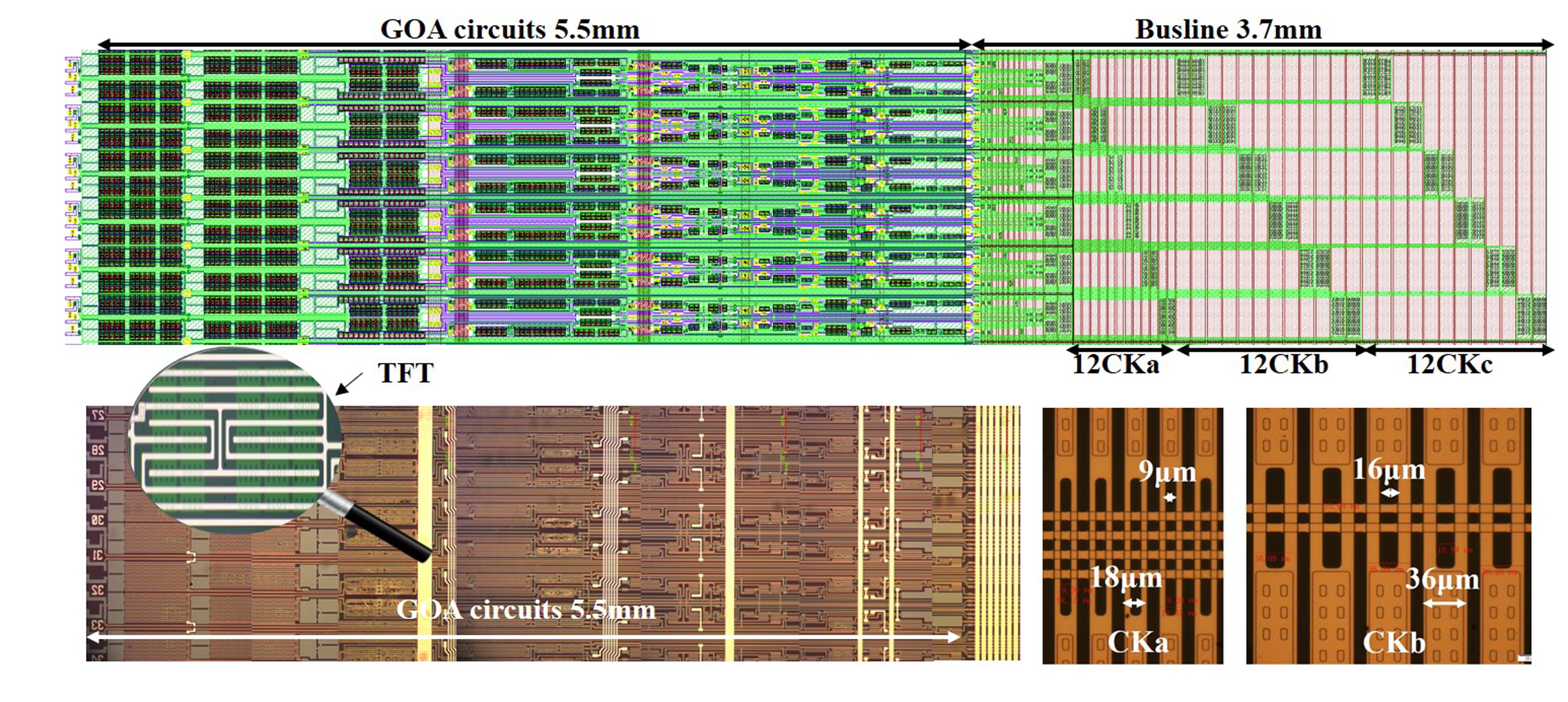
Figure 6 shows the layout of GOA with a width of 9.2mm, which is fabricated through top emission AMOLED manufacturing process in a G4.5 experimental line. To investigate GOA function, an oscilloscope was utilized to testify output waveforms from GOA, the results of which can be seen in Figure 7. During this frame, the system is set to carry out mobility compensation operation at the first stage of GOA, which can be successfully detected at blank time in Figure 7(a). Meanwhile, the measured output waveform of the 2160th stage is shown in Figure 7(b). GOA yield rising time (RT) and falling time (FT) of 5.2µs and 3.6µs for the GOA in the left side of display, respectively, as well as 5.5µs and 3.8µs for the right side. Theoretically, charging rate is equal to discharging rate for a stable signal source.
As a measure to maintain comparability, RT must be modified to the same level with FT (from -6V to 20V) because the potential difference at the rise stage is higher. After voltage modification, RT is decreased to 4.3µs for the left GOA and 4.5µs for the right GOA. The slight difference between RT and FT is due to the potential driving force difference during charging (0.15µs) stage and discharging (0.1µs) stage in external chips. The resistive load and capacitance load extracted from simulation tool for each scan line are 4.1K and 850pF (τ=3.5µs), respectively. Besides scan line, the RC loading in CK line is another important factor to affect the transport speed of signals. Depending on simulation result, the resistive load and capacitance load for each CK line are 0.26K and 884pF (τ=0.22µs), respectively. It can be easily concluded that the total delay time (τ=3.72µs) from simulation results fits well with the experimental FT result, illustrating that the discharging rate is fast enough to release the voltage in scan lines.
It has been found out that TFT characterization can be gradually recovered toward its initial performance after electric stress operation [32,33]. Since the display is turned off and stored under circumstance of room temperature for 2h, the output voltage recovers from 5.7V to 8.5V, illustrating that malfunction of GOA is caused by the deterioration of TFT performance. When display is turned on, the image in display starts to deteriorate. The working temperature, total current, luminance and OLED efficiency generated by display increase monotonically with operation time. The observation of stripe mura in Figure 8(a) suggests that the picture is affected by the variety of mobility in TFTs. External compensation technology is performed to eliminate the influence of mobility difference to image quality. Obviously, display image with high quality has been obtained after mobility compensation, shown in Figure 8(b).
5. Conclusions
We have demonstrated the feasibility of mobility compensation technology employing with GOA circuits in AMOLED displays. The working mechanisms of mobility compensation method and GOA technology are systematically investigated. Through the integration of a logical sense unit in GOA, driving pulses for mobility compensation process in pixels have been generated in scan signals at blank time. Moreover, due to the utilization of STT and dual VGL power signals, the depletion-mode TFTs can be completely turned off and GOA exhibits high stability with Vth process margin from -5V to 5V. Experimental results confirm that sequential pulse signals can be periodically transferred stage by stage in GOA. Finally, the image quality in display improves significantly by the introduction of mobility compensation technology.
Funding
This research received no external funding.
Acknowledgments
We gratefully acknowledge the funding from Shenzhen Science and Technology Program under grant (KJZD20230923114412026), and the Scientific Research Startup Fund for Shenzhen High-Caliber Personnel of SZPT (6022310051K, 6022310034K, LHRC20220402-2025) for this work.
Conflicts of Interest
The authors declare no conflict of interest.
References
- D. S. Salehi, S. Jung, B. C. Kim, J. H. Noh, I. S. Lee, N. B. Choi, S. Y. Park, H. J. Kim. Improvement of flicker phenomenon at low frequencies in AMOLED displays by applying compensation scheme of variable reset voltage. Scientific Reports, vol. 15, no. 1, pp. 12181, 2025. [CrossRef]
- Y. Shen, F. H. Chen, D. Yu, X. Liu, Y. Ma, X. Zhang, F. Cheng, X. Zhu, X. Zou. TFT Backplanes Doped by BF2 Ion for Improved Stability and AMOLED Display Quality. Advanced Electronic Materials, 2400989, 2025. [CrossRef]
- Y. Hu, L. Q. Guo, C. Huo, M. Dai, J. Ding. Transparent nano thin-film transistors for medical sensors, oled and display applications. International Journal of Nanomedicine, vol. 15, pp. 3597-3603, Jun, 2020. [CrossRef]
- J. Jin. W. Xu, L. Cheng. A Hybrid Single-Inductor Bipolar-Output Converter With a Concise PWM Control for AMOLED Displays. IEEE Journal of Solid-State Circuits, vol. 15, no. 1, pp. 4150-4161, 2024.
- Y. J. Lim, J. H. Yu, K. H. Song, M. H. Lee, H. Ren, B. J. Mun, G. D. Lee, S. H. Lee. Film patterned retarder for stereoscopic three-dimensional display using ink-jet printing method. Optics Express, vol. 22, no. 19, pp. 22661-22666, Sep, 2014. [CrossRef]
- T. Y. Zhao, D. D. Zhang, T. Y. Qu, L. L. Fang, Q. B. Zhu, Y. Sun, T. H. Cai, M. L. Chen, B. W. Wang, J. H. Du, W. C. Ren, X. Yan, Q. W. Li, S. Qiu, D. M. Sun. Flexible 64 × 64 Pixel AMOLED Displays Driven by Uniform Carbon Nanotube Thin-film Transistors. ACS Applied Materials & Interfaces, vol. 11, pp. 11699-11705, Mar, 2019. [CrossRef]
- W. J. Wu, L. R. Zhang, Z. P. Xu, L. Zhou, H. Tao, J. H. Zou, M. Xu, L. Wang, J. B. Peng. A High-Reliability Gate Driver Integrated in Flexible AMOLED Display by IZO TFTs. IEEE Transactions on Electron Devices, 2017, vol. 64, no. 5, pp.1991-1996, 2017. [CrossRef]
- W. J. Wu, J. W. Chen, J. S. Wang, L. Zhou, H. Tao, J. H. Zou, M. Xu, L. Wang, J. B. Peng, M. Chan. High-Resolution Flexible AMOLED Display Integrating Gate Driver by Metal Oxide TFTs. IEEE Electron Device Letters, PP. 1-1, 2018. [CrossRef]
- C. L. Lin, C. C. Hsu, P. S. Chen, P. C. Lai, P. T. Lee, P. Y. Kuo. Suppressing VTH Variations in LTPS Thin-Film Transistors With Current Scaling Ratio Modulation for AMOLED Display. IEEE Transactions on Electron Devices, PP. 1-5, June, 2018. [CrossRef]
- Y. Zhang, J. Li, R. Li, D. T. Sbircea, A. Giovannitti, J. Xu, H. Xu, G. Zhou, L. Bian, I. McCulloch, N. Zhao. Liquid-solid dual-gate organic transistors with tunable threshold voltage for cell sensing. Acs Applied Materials & Interfaces, vol. 9, pp. 38687-38694, Oct, 2017. [CrossRef]
- J. Y. Huh, S. B. Seo, H. S. Park, J. H. Jeon, H. H. Choe, K. W. Lee, J. H. Seo, M. K. Ryu, S. H. Ko Park, C. S. Hwang. Light and bias stability of a-IGZO TFT fabricated by r.f. magnetron sputtering. Current Applied Physics, vol. 11, pp. s49-s53, May, 2011. [CrossRef]
- Y. Zhang, G. Han, M. Qin, Y. Shen, X. Lu, Y. Yi, N. Zhao. Spectroscopic Study of Charge Transport at Organic Solid–Water Interface. Chemistry of Materials, vol. 30, pp. 5422-5428, July, 2018. [CrossRef]
- C. L. Lin, Y. C. Chen. A novel LTPS-TFT pixel circuit compensating for TFT threshold-voltage shift and OLED degradation for AMOLED. IEEE Electron Device Letters, vol. 28, no. 2, pp. 129-131, Feb, 2007. [CrossRef]
- Y. Zhang, W. Chen. A new LTPS TFT AC pixel circuit for an AMOLED. Journal of Semiconductors, vol. 34, no. 1, pp. 015009, Jan, 2013. [CrossRef]
- T. Goto, K. Saito, F. Imaizumi, M. Hatanaka, M. Takimoto, M. Mizumura, J. Gotoh, H. Ikenoue, S. Sugawa. LTPS Thin-Film Transistors Fabricated Using New Selective Laser Annealing System. IEEE Transactions on Electron Devices, PP:1-7, May, 2018. [CrossRef]
- J. S. Lee, S. Chang, S. M. Koo, S. Y. Lee. High-Performance a-IGZO TFT with gate dielectric fabricated at room temperature. IEEE Electron Device Letters, vol. 31, no. 3, pp. 225-227, Mar, 2010. [CrossRef]
- Y. S. Chun, S. Chang, S. Y. Lee. Effects of gate insulators on the performance of a-IGZO TFT fabricated at room-temperature. Microelectronic Engineering, vol. 88, no. 7, pp. 1590-1593, Feb, 2011. [CrossRef]
- Y Kusaka , N. Shirakawa , S. Ogura, J. H. Leppaniemi, A. Sneck, A. Alastalo, H. Ushijima, N. Fukuda. Reverse offset printing of semidried metal acetylacetonate layers and its application to a solution-processed IGZO TFT fabrication. ACS Applied Materials & Interfaces, pp. 1-12, Jul, 2018. [CrossRef]
- J. Kim, S. Bang, S. Lee, S. Shin, J. Park, H. Seo, H. Jeon. A study on H2 plasma treatment effect on a-IGZO thin film transistor. Journal of Materials Research, vol. 27, no. 17, pp. 2318-2325, June, 2012. [CrossRef]
- Z. Zong, L. Li, J. Jang, N. Lu, M. Liu. Analytical surface-potential compact model for amorphous-IGZO thin-film transistors. Journal of Applied Physics, 2015, vol. 117, no. 21, pp. 400-405, June, 2015. [CrossRef]
- H. J. Shin, S. Takasugi, W. S. Choi, M. K. Chang, J. Y. Choi, S. K. Jeon, S. H. Yun, H. W. Park, J. M. Kim, H. S. Kim, C. H. Oh. A novel OLED display panel with high-reliability integrated gate driver circuit using IGZO TFTs for large-sized UHD TVs. Sid International Symposium Digest of Technology Papers, vol. 28, no. 2, pp. 358-361, 2018.
- S. Takasugi, H. J. Shin, M. K. Chang, S. M. Ko, H. J. Park, J. P. Lee, H. S. Kim, C. H. Oh. Advanced compensation technologies for large-sized UHD OLED TVs. Journal of the Society for Information Display, 2016, vol. 24, no. 7-9, pp. 410-418, Apr, 2016. [CrossRef]
- B. Kim, S. C. Choi, S. Y. Lee, S. H. Kuk, Y. H. Jang, C. D. Kim, M. K. Han. A depletion-mode a-IGZO TFT shift register with a single low-voltage-level power signal. IEEE Electron Device Letters, vol. 32, no. 8, pp. 1092-1094, Jane, 2011. [CrossRef]
- X. Li, D. Geng, M. Mativenga, J. Jang. High-speed dual-gate a-IGZO TFT-based circuits with top-gate offset structure. IEEE Electron Device Letters, vol. 35, no. 4, pp.461-463, Apr, 2014. [CrossRef]
- B. Kim, S. C. Choi, S. H. Kuk, Y. H. Jang, K. S. Park, C. D. Kim, M. K. Han. A novel level shifter employing IGZO TFT. IEEE Electron Device Letters, vol. 32, no. 2, pp.167-169, Feb, 2011. [CrossRef]
- Y. Xue, C. H. Fang , B. X. Han, A. G. Tu, Z. G. Yang, G. Chaw, C. W. Liao, S. D. Zhang, Y. C. Wu, P. Y. Lu. Panel design technology for a 31-inch GOA drived AMOLED display with BYYB OLED structure and slim border, SID Symposium Digest of Technical Papers. vol. 60, no. 1, pp. 846-849, 2019. [CrossRef]
- D. H. Kim, H. J. Koo, M. G. Kang, K. Chun, U. Choi, Y. Ko, J. Jeon, C. Y. Jeong, Y. H. Jang, J. U. Bae, K. S. Park, S. Y. Yoon, I. B. Kang, Gate driver circuits for internal compensation type OLED display with high mobility oxide TFT. Sid Symposium Digest of Technical Papers, vol. 49, no. 1, pp. 40-43, 2018. [CrossRef]
- C. L. Lin, P. C. Lai, P. C. Lai, T. C. Chu, C. L. Lee. Bidirectional gate driver circuit using recharging and time-division driving scheme for in-cell touch LCDs. IEEE Transactions on Industrial Electronics, 2017. [CrossRef]
- B. Kim, H. N. Cho, W. S. Choi, S. H. Kuk, J. S. Yoo, S. Y. Yoon, M. Jun, Y. K. Hwang, M. K. Han. A novel depletion-mode a-IGZO TFT shift register with a node-shared structure. IEEE. Electron Device Letters, vol. 33, no. 7, pp. 1003-1005, Jul, 2012. [CrossRef]
- J. S. Kim, J. W. Byun, J. H. Jang, Y. D. Kim, K. L. Han, J. S. Park, B. D. Choi. A high-reliability carry-free gate driver for flexible displays using a-IGZO TFTs. IEEE Transactions on Electron Devices, 2018, vol. 65, no. 8, pp. 3269-3276, May, 2018. [CrossRef]
- C. L. Lin, M. H. Cheng, C. D. Tu, M. C. Chung. Highly reliable integrated gate driver circuit for large TFT-LCD applications. IEEE Electron Device Letters, vol. 33, no. 5, pp. 679-681, 2012. [CrossRef]
- M. Marinkovic, R. Takata, A. Neumann, D. V. Pham, R. Anselmann, J. Maas, J. L. Steen, G. Gelinck, I. Katsouras. Large-Area Processing of Solution Type Metal-Oxide in TFT Backplanes and Integration in Highly Stable OLED Displays. Sid International Symposium Digest of Technology Papers, vol. 14, no. 1, pp. 169-172, 2017.
- Y. Hara, T. Kikuchi, H. Kitagawa, J. Morinaga, H. Ohgami, H. Imai, T. Daitoh, T. Matsuo. IGZO-TFT Technology for Large-screen 8K Display. Sid International Symposium Digest of Technology Papers, vol. 53, no. 3, pp. 706-709, 2018. [CrossRef]
Figure 1.
The outline of external compensation system in displays.
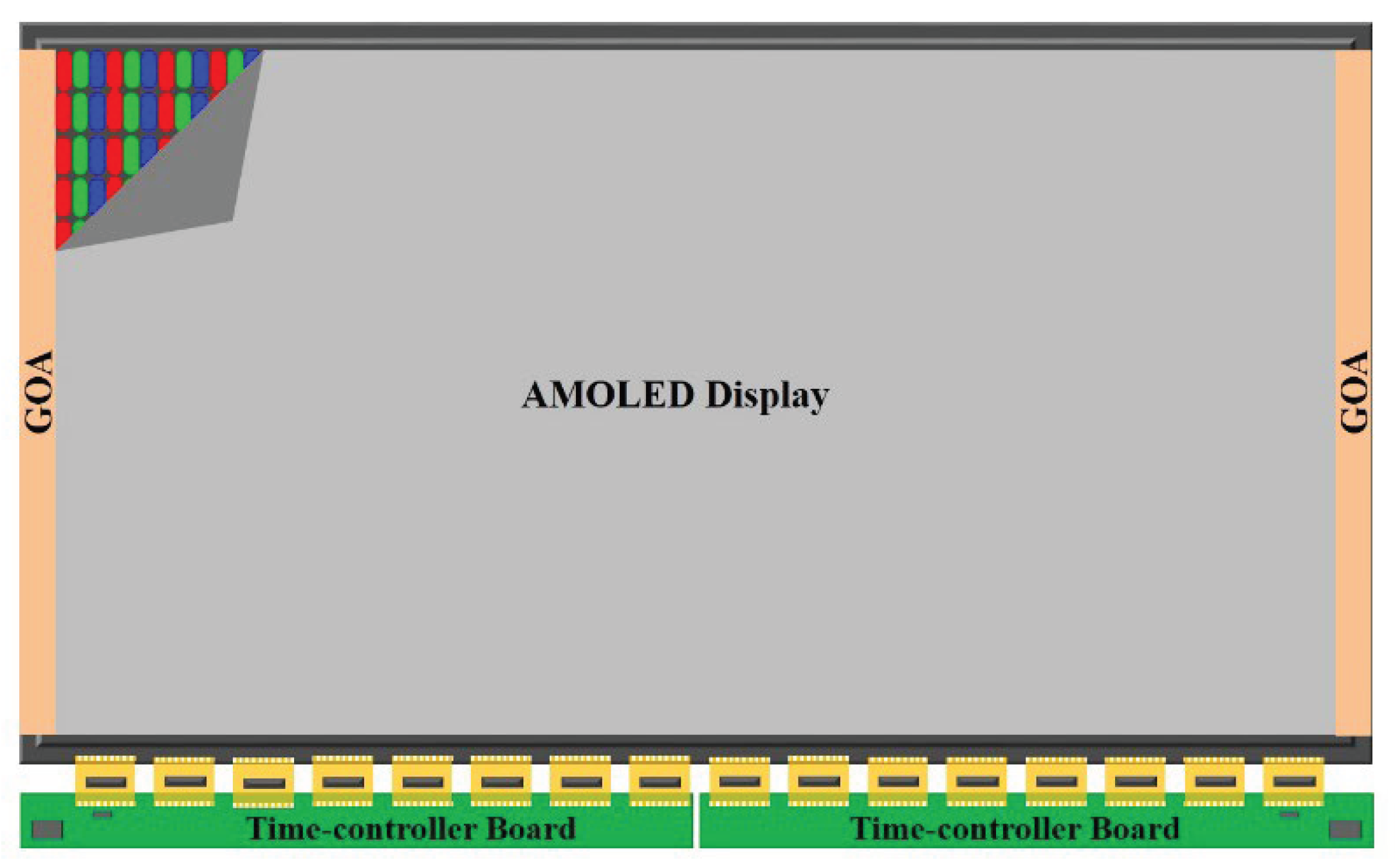
Figure 2.
(a) Schematic of external compensation system; (b) timing diagram at emission stage; (c) timing diagram at compensation stage.
Figure 2.
(a) Schematic of external compensation system; (b) timing diagram at emission stage; (c) timing diagram at compensation stage.

Figure 3.
The time diagram of (a) normal scan signal; (b) scan signal with mobility compensation function.
Figure 3.
The time diagram of (a) normal scan signal; (b) scan signal with mobility compensation function.
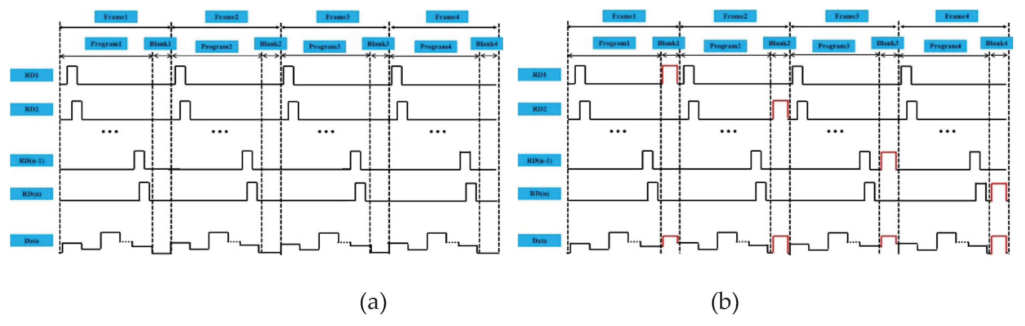
Figure 4.
(a) Schematic; (b) time diagram of proposed GOA.
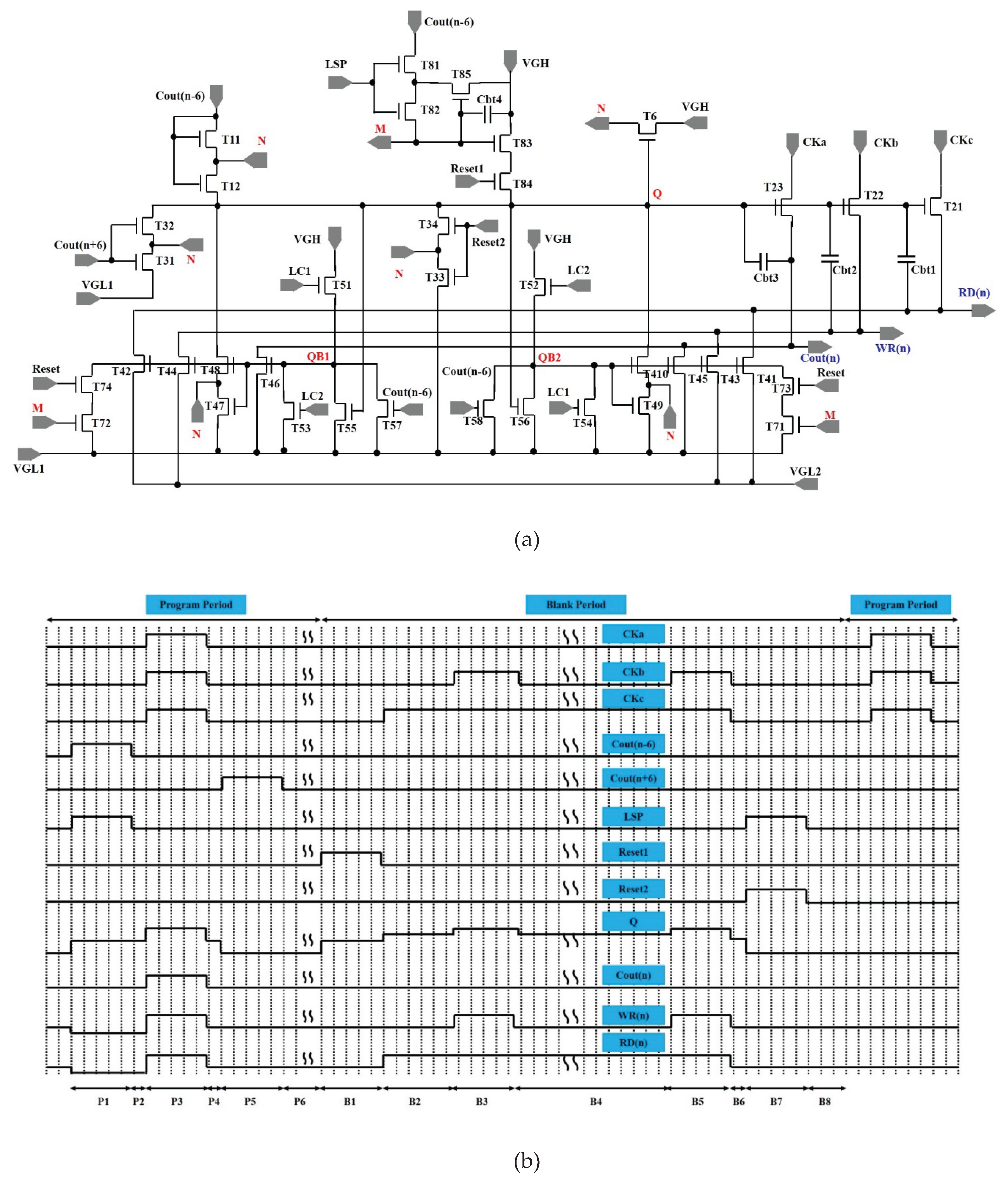
Figure 5.
(a) Measured and simulated transfer curves of IGZO TFT; (b) Simulation result of output waveforms when Vth shift by 0V and -6V; (c) Simulation result of output waveforms when Vth shift by 0V and 6V.
Figure 5.
(a) Measured and simulated transfer curves of IGZO TFT; (b) Simulation result of output waveforms when Vth shift by 0V and -6V; (c) Simulation result of output waveforms when Vth shift by 0V and 6V.
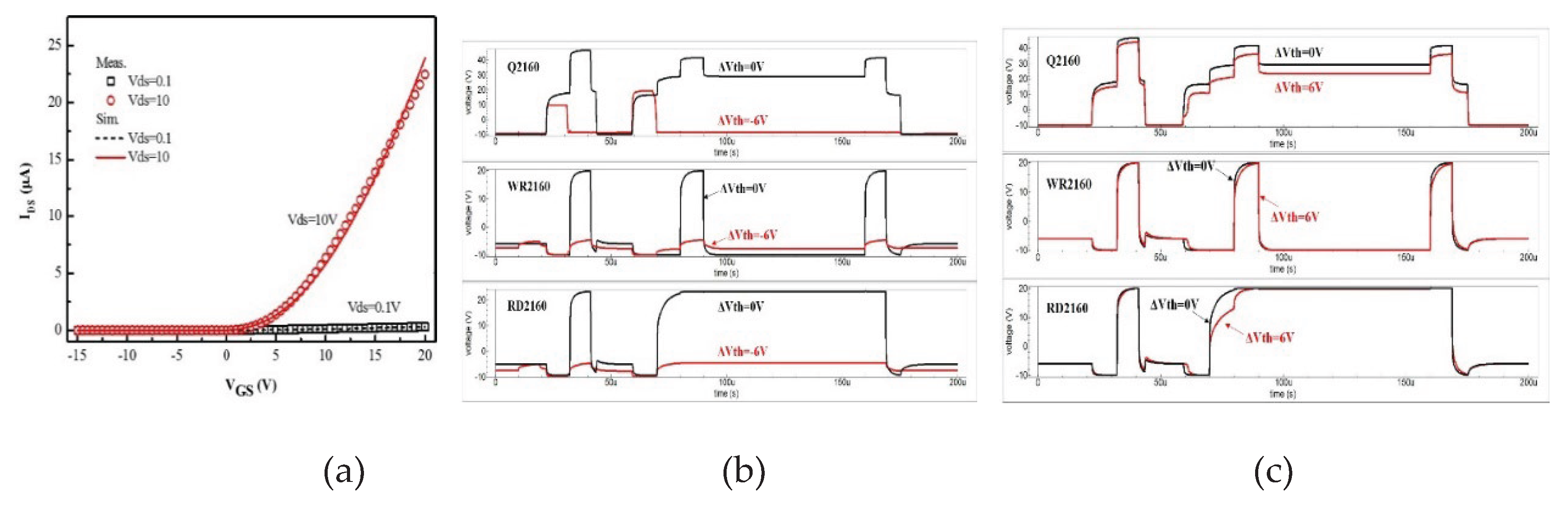
Figure 6.
Detailed layout of GOA.
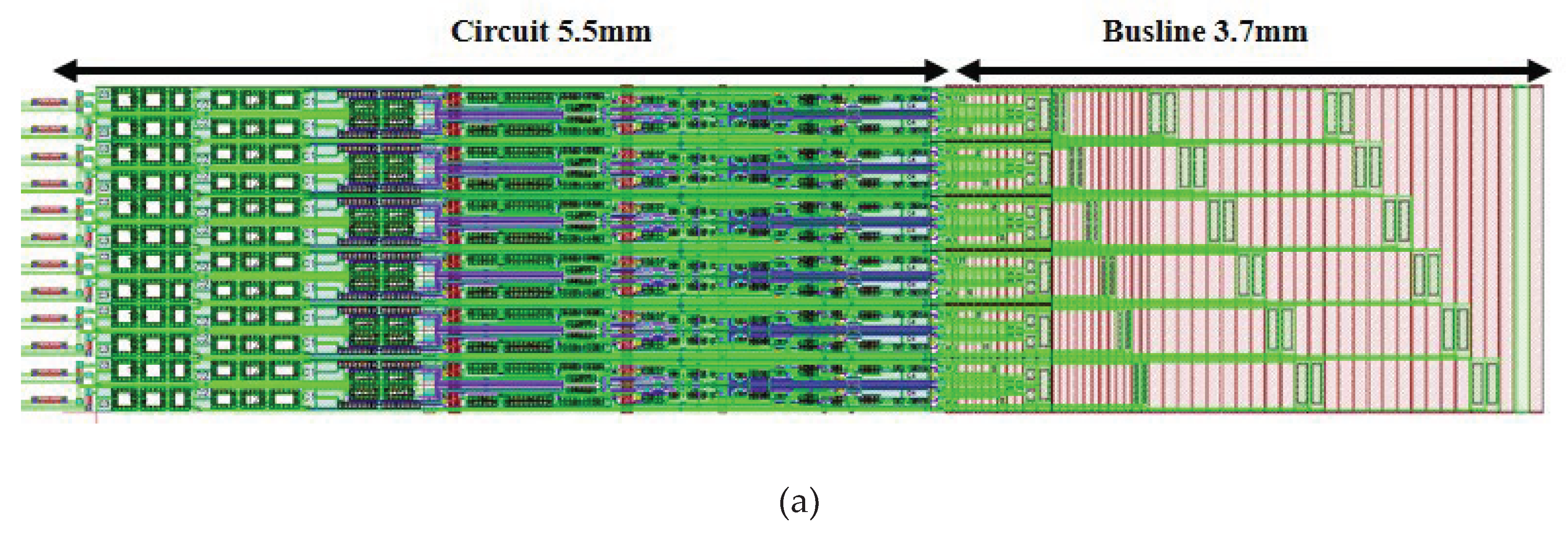
Figure 7.
GOA waveform (a) at blank time for the first stage; (b) for the 2160th stage.
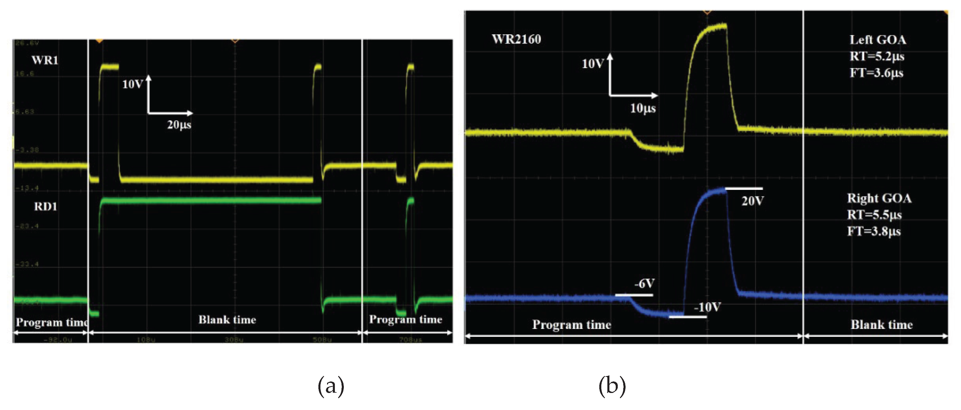
Figure 8.
Display image (a) before compensation; (b) after compensation.
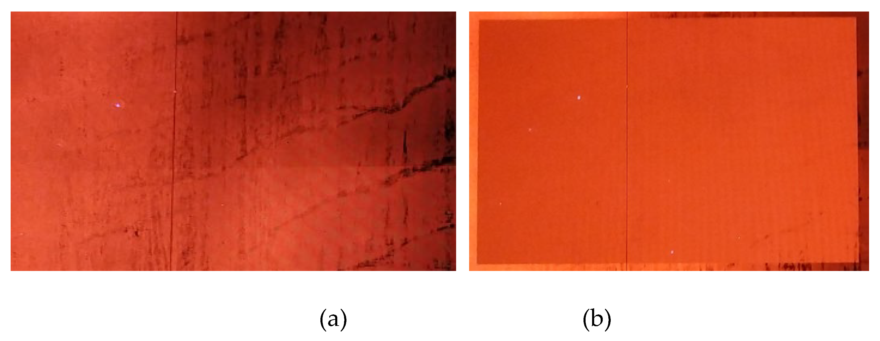

Table 1.
Parameters of devices in goa circuit.
| TFT/Capacitance Size | |
|---|---|
| T11/T12/T21 | 500µm/6.5µm |
| T22/T23 | 2500µm/6.5µm |
| T31~T34/T47~T410/T81~T84 | 100µm/6.5µm |
| T41~T44 | 300µm/6.5µm |
| T45/T46 | 150µm/6.5µm |
| T51/T52 | 10µm/8µm |
| T53~T56/T71~T74 | 50µm/6.5µm |
| T57/T58 | 25µm/6.5µm |
| T6 | 15µm/15µm |
| Cbt4 | 2.5pF |
| Cbt1/Cbt2/Cbt3 | 1.25pF |
Table 2.
Amplitude of input signals.
| GOA Input Signals | |
|---|---|
| CKa1~CKa12/CKb1~CKb12/CKc1~CKc12 | -10V~20V |
| LSP/Reset1/Reset2 | -10V~20V |
| LC1/LC2/STV | -10V~20V |
| VGH | 20V |
| VGL1 | -10V |
| VGL2 | -5V |
Disclaimer/Publisher’s Note: The statements, opinions and data contained in all publications are solely those of the individual author(s) and contributor(s) and not of MDPI and/or the editor(s). MDPI and/or the editor(s) disclaim responsibility for any injury to people or property resulting from any ideas, methods, instructions or products referred to in the content. |
© 2025 by the authors. Licensee MDPI, Basel, Switzerland. This article is an open access article distributed under the terms and conditions of the Creative Commons Attribution (CC BY) license (http://creativecommons.org/licenses/by/4.0/).
Copyright: This open access article is published under a Creative Commons CC BY 4.0 license, which permit the free download, distribution, and reuse, provided that the author and preprint are cited in any reuse.


