
Submitted:
15 October 2025
Posted:
20 October 2025
You are already at the latest version
Abstract
The permanent memory effect in Polymer Dispersed Liquid Crystal (PDLC) systems imparts unique properties to these devices, making them well-suited for digital memory applications. By investigating the impact of homogeneous alignment layer types on this effect, we successfully developed and tested a proof-of-concept prototype capable of recording information in both opaque and transparent states within a digital process.
Keywords:
polymer dispersed liquid crystal (PDLC)
; digital memory
; surface alignment layers
; information storage
1. Introduction
Liquid crystals (LCs) are a distinctive class of materials that possess properties intermediate between those of liquids and solid crystals, making them vital in various electro-optical applications, including displays and memory devices. The orientation of LC molecules, which is heavily influenced by surface alignment techniques, plays a crucial role in shaping their electro-optic response. When LC directors align along a specific axis, this ordered structure allows molecular dipoles to orient accordingly—a process that becomes especially significant under an electric field. Applying such a field induces weak dipoles that collectively create a net polarization, thereby boosting the field-induced reorientation of the liquid crystal.
However, the interaction of LCs with different substrate materials used in electro-optical devices can substantially influence their alignment. On Indium-Tin-Oxide (ITO) surfaces, the dominant van der Waals interactions between the substrate and LC molecules often weaken the intermolecular forces within the liquid crystal itself, leading to random surface alignment [1]. This disruption hampers bulk orientational order and restricts the effectiveness of a perpendicular electric field (∆ε > 0), as the strong surface anchoring tends to maintain the initial LC orientation, ultimately limiting the electro-optical response. Conversely, in configurations where homogeneous alignment is achieved, the directors of the LCs align parallel to the substrate, propagating this order into the bulk through intermolecular elastic interactions [2]. Surface molecules align with the polymer substrate to minimise surface free energy, thus reinforcing homogeneous alignment and increasing responsiveness under electric fields [1].
The orientation of LC directors under an applied electric field results from a dynamic balance between surface anchoring and dielectric torque, involving a careful interplay of elastic, electric, and interfacial contributions to the nematic free energy. In dielectrically positive liquid crystals, the orientation follows an out-of-plane rotation parallel to the field, whereas, in homeotropic alignments with dielectrically negative characteristics, the rotation is perpendicular to the field. Once the electric field is removed, the orientation of the liquid crystal bulk is dictated by boundary anchoring, which aims to minimise elastic energy. In memory-enabled systems, a sufficiently strong electric field can induce reorientation in both surface and bulk LC molecules, establishing a new preferred surface anchoring that can maintain this alignment even after the field is removed [3]. Interestingly, in configurations lacking alignment layers (e.g., ITO-only substrates), surface directors remain unchanged, preventing tilt above the threshold voltage and causing the bulk LCs to revert to a random configuration once the field is withdrawn.
Optical information storage in LC composites has been demonstrated previously [4,5,6,7,8,9,10,11,12,13], and the permanent memory effect of PDLCs developed in this study enables the design of novel digital memory devices based on write–read–erase cycles. While alignment layers have minimal impact on conventional Polymer Dispersed Liquid Crystal PDLC performance [14,15,16,17] —which lacks permanent memory—this work investigates their role in inducing a permanent memory effect. The developed PDLC exhibits 70% permanent memory, thermal stability, and reproducibility over multiple electric and thermal cycles, demonstrating its suitability for digital information recording, storage, and erasure via write–read–erase cycles.
2. Experimental
2.1. Materials and Methods
Nematic liquid crystalline mixture E7 was purchased from Merck. It is a eutectic mixture exhibiting a positive dielectric anisotropy at T = 20º and a nematic-isotropic transition temperature of TNI = 58ºC. It contains 4-cyano-4’-pentyl-1,1’-biphenyl (51%), 4-n-heptyl-4’-cyanobiphenyl (25%), 4,4’-n-octyloxycyanobiphenyl (16%), 4’-n-pentyl-4-cyanotriphenyl (8%) wt./wt.16. The initiator for the thermal polymerization was 2,2’-azobis(isobutyronitrile) (AIBN) purchased from Aldrich (used as received). The pre-polymer used was poly(ethyleneglycol) dimethacrylate with molecular weight 875 g mol-1 (PEGDM875) and was previously passed through a disposable inhibitor remover column from in order to eliminate the hydroquinone stabilizer, both from Aldrich.
2.2. Preparation of PDLCs Test Cells
The PDLCs were prepared by a homogeneous solution of 70 wt.-% (percentage by weight) of LC E7 and 30 wt.% of poly(ethyleneglycol) dimethacrylate with molecular weight 875 g mol-1 (PEGDM875) and 1 wt.% of thermal initiator, N,N-azobisisobutyronitrile (AIBN), that filled manufactured or commercial cells. The manufactured cells were constructed by a pair of commercial flat glass substrates model D256A-X000 provided by Instec Inc. (Figure 1). They are ITO (100 Ω; 0.023 ± 0.005 µm in thickness) coated glass substrates (soda-lime glass type) that were covered with a rubber polyimide (KPI-300B type) alignment layer to promote homogeneous alignment.
For cell assembly, glass substrates are spaced by a Mylar film formed along the edges, such that the faces of the glass substrates form a gap. The mylar spacer, which fixes the thickness of the gap, is about 23 µm thick. The substrates are held together by applying a sealing epoxy resin along the edge contour except for an inlet area where the pre-polymer and E7 mixture will be injected into the spacing between substrates.
The commercial cells supplied from Instec Inc. (Figure 2) have the same substrate features as ITO (100 Ω; 0.023 ± 0.005 µm of thickness) and a coated glass substrate (soda lime glass type) that was covered with a rubber polyimide (KPI-300B) alignment layer, also to promote a homogeneous alignment. The thickness of cells is about 20 µm.
Six types of PDLC cells were constructed by allowing the unidirectional rubbing direction of polyimide. An ITO-coated glass substrate that was covered with a rubber polyimide alignment layer on the upper glass substrate, to be perpendicular, parallel and anti-parallel to that at the lower glass substrate, with a cell gap of 23 μm by Mylar spacers. The cells were denoted by Perpendicular-PDLC, Parallel-PDLC and anti-parallel-PDLC, respectively. It is also assembled a cell with random planar alignment by non-rubbed ITO coated glasses and the cell gap was also ensured to be 23 μm by mylar spacers. This cell was denoted as ITO-PDLC. It was also prepared cells with homeotropic alignment by orientation layers with lecithin (lecithin-PDLC). Finally, it was also compared to a homogeneous alignment in anti-parallel configurations of unidirectionally rubbed polyimide orienting substrates in a commercial LC cell with 20 μm.
A handmade oven was used in thermal polymerizations, equipped with an auto-tune temperature controller provided by CAL Controls, model CAL 3300, and a resistance thermometer, Pt100/RTD-2, whose sensor has a temperature range from -200 to 400ºC.
2.3. Electro-Optical Characterization of PDLC Test Cells
For electro-optical characterization of PDLC films, the optical transmittance was measured by increasing and then decreasing the voltage applied to the cell. The light transmittance studies were performed using a diode array Avantes spectrophotometer (AvaLight-DHS and AvaSpec 2048) with a halogen lamp and optical fiber connections. A 633 nm wavelength was selected. The electric pulse (1 kHz) was generated by a programmable waveform generator (Wavetek 20MHz Synthesised Function Generator Model 90), producing alternating current (AC) wave with low amplitude (between 0 and 27 VRMS) for sample excitation. For the electro-optical measurements, an external electric field was applied across the PDLC film. The generator connected to a Vtrek TP-430 amplifier reaching a voltage of 47VRMS was linked to a 220V/9V transformer inversely connected and it increased the applied voltage by a factor of 24. A resistance (1Ω) had the purpose of securing the amplifier from short-circuits and another resistance (150kΩ) was used to standardize the voltage wave output. The amplifier was fed by a Kiotto KPS 1310 power supply. The output detector (AvaSpec-2048) was connected to a computer software data acquisition.
2.4. Conoscopic Observations of Liquid Crystal
The influence of alignment layer surfaces on the orientation of E7 liquid crystal molecules was confirmed through conoscopic observations using a monochromatic convergent beam in a glass LC cell. When the E7 n-director is parallel to the light path, a Maltese cross appears at the center of the field, as shown in Figure 3a. This demonstrates that, in a homeotropically aligned LC cell, the optic axis is oriented normal to the substrate surface. In contrast, in cells with homogeneous alignment produced by rubbed polyimide, the E7 n-directors orient parallel to the substrate surface, as illustrated in Figure 3b.
2.5. Electro-optical Properties of PDLC Test Cells
The electro-optical properties of PDLCs films were compared and it was found that the presence of an alignment layer greatly affected the permanent memory effect (Figure 4).
The enhancement of the permanent memory effect (PME) in PDLCs can be attributed to the influence of surface alignment layers. In the PEGDM875/E7 system, mesogenic molecules begin ordering at the substrate interface. During polymerization-induced phase separation, LC domains disperse within the polymer matrix while remaining anchored to the substrate according to its surface orientation [1]. Substrate anchoring can propagate into the bulk, with a thin layer of free LC potentially forming between the LC/polymer domains and the alignment layer [17].
In PDLCs without alignment layers (ITO substrates), nematic directors exhibit random planar orientation at the interface, whereas alignment layers impose controlled orientations: homogeneous alignment along the polyimide rubbing direction or homeotropic alignment via lecithin. The polymer-ball morphology, characterized by interconnected LC channels within polymer agglomerates, facilitates the transmission of surface anchoring into the bulk. This suggests a self-alignment mechanism of LC–prepolymer chains at substrate interfaces, as illustrated in Figure 5.
Under an applied electric field, the LC directors in the PDLC domains align parallel to the field, allowing incident light to pass through without scattering by matching the LC’s ordinary refractive index to that of the polymer matrix, rendering the PDLC transparent. Upon removal of the field, PDLCs with homogeneous alignment maintain a higher transparency (Figure 4c–f), whereas in ITO-PDLC cells, the scattering state is restored (Figure 4b).
Homeotropic anchoring yields high initial transparency (~30%) in the OFF state, as LC molecules are preferentially oriented perpendicular to the cell surface. Even without an applied field, light passes through the PDLC with minimal scattering due to refractive index matching (Figure 4a).
The key distinction between these PDLCs is the alignment layer at the glass-cell boundaries. In homogeneous PDLCs, the applied electric field can disturb the LC directors at the alignment surfaces. After the field is removed, these surface-oriented LC directors influence the bulk LC phase—dispersed continuously in the polymer matrix—stabilizing a new alignment state different from the initial configuration, thus enabling a permanent memory effect.
In contrast, in ITO-PDLC cells, the random planar orientation of LC molecules at the ITO surface is largely unaffected or only partially disturbed by the field. Upon field removal, elastic reorientation drives the bulk LC back to its minimal-energy state imposed by the random surface alignment, restoring light scattering (Figure 4b).
The next step is to evaluate the previously studied PDLC films for their potential in digital memory devices using a passive PDLC matrix.
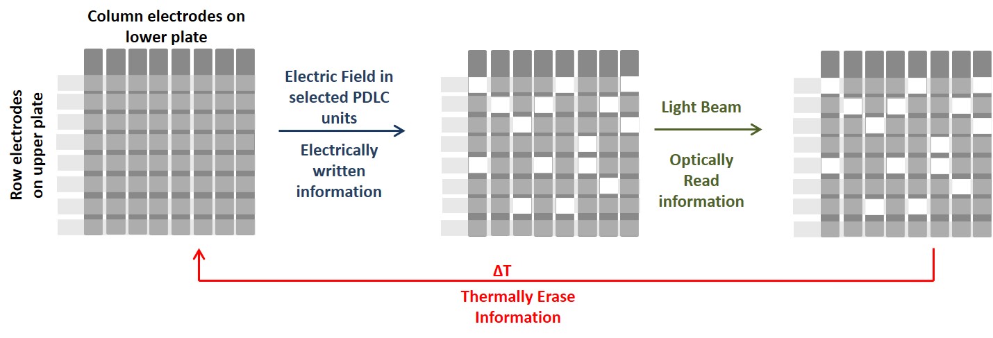
3. Manufacturing Passive PDLC Film Matrixes: Digital Memory PDLCs Devices Based on Electrical Writing Digital Information
Optical information storage in PDLCs exploits electrically written, optically read, and thermally erased operations within a multiplexed pixel array, where each pixel is a PDLC unit exhibiting a permanent memory effect (PME). Pixels are individually addressable, switching between transparent (ON) and opaque (OFF) states depending on the applied electric field.
In a passive-matrix configuration (Figure 6), conducting rows and columns serve as electrodes for selective pixel addressing. Applying an electric field to a pixel switches it to the transparent state, while unaddressed pixels remain opaque. Transparency is maintained after field removal due to the PME. Stored information can be optically read and erased thermally (up to the LC’s TNI), enabling repeated write–read–erase cycles.
3.1. Pattern Fabrication on ITO Covered with an Alignment Layer
The PDLCs with a permanent memory effect developed in this work provide a foundation for further investigations into their use as optical storage materials. To explore this application, a passive PDLC matrix display with an 8×8 pixel array, each pixel measuring 1×1 mm², was fabricated. A critical step in the fabrication process is the formation of patterned ITO substrates, achieved using photolithography.
The photolithography process begins by spin-coating a 16×16 mm ITO-coated glass substrate (20×25×1.1 mm) covered with a rubbed polyimide alignment layer with a positive photoresist, AZ-1518, which contains the photoactive compound diazonaphthoquinone (DNQ) [20]. After coating, the substrate is soft-baked at 110 °C for 4 minutes to remove solvents and improve adhesion. The developed photomask is then aligned in contact with the substrate, selectively exposing certain areas of the photoresist to UV light for several seconds.
Exposure to UV light induces chemical changes in the photoresist: the nitrogen atom is released from the aromatic ring, generating a highly reactive vacant orbital. One carbon atom shifts out of the ring and covalently bonds to an oxygen atom (Wolff rearrangement). In the presence of water, a subsequent rearrangement converts a double bond on the external carbon into a single bond with a hydroxyl group, producing a carboxylic acid that is more soluble in the NaOH developing solution than the original photoresist [20].
After development, the remaining photoresist serves as a mask for etching. Exposed polyimide areas are etched using an O₂–SF₆ plasma [21,22], and exposed ITO areas are chemically etched in aqua regia (HCl:HNO₃) by immersing the substrate vertically for 1 minute at 40 °C without stirring, as the etch rate increases with temperature. The photoresist is subsequently stripped with acetone, revealing line-shaped ITO electrodes with a width of 1 mm and a spacing of 1 mm, as shown in Figure 7.
Following the generation of the photomask, the lithography process can be schematic proceed as shown in Figure 8.
3.2. Line-shaped ITO Electrodes Covered with Polyimide Thickness Measurement
A mechanical profilometer (Ambios XP-Plus 200 Stylus) was used to estimate the film thickness of each eight line-shaped ITO covered with polyimide (PI) previously development in the photolithography process, as illustrated by Figure 9 a). In average each line has a thickness of 160nm. The line thickness profile exemplification is shown in Figure 9 b).
3.3. PDLC Passive Matrix Device Assembly
To demonstrate the principle of passive-matrix addressing, devices were constructed by sandwiching the PDLC mixture between two glass substrates. The top and bottom electrodes were patterned ITO layers coated with polyimide, arranged in perpendicular rows and columns (or vice versa). The intersection of a row and column defines a single display element, referred to as a pixel.
The cell thickness was maintained using 23 µm Mylar spacers along the substrate perimeter, sealed with epoxy resin. The cavity was filled with the PDLC mixture—PEGDM875 (1 wt.% AIBN) and E7 in a 30:70 wt.% ratio—via capillary action, and the cell was subsequently cured at 70 °C overnight. Each pixel corresponds to a PDLC unit located at the intersection of the row and column electrodes. The rows and columns are connected to integrated circuits that selectively apply voltage to individual pixels. Key specifications of the passive-matrix PDLC device are summarized in Table 1.
3.4. PDLC Passive Matrix Device Operation
The macroscopic effect of electrically written information in a passive PDLC matrix device was directly observed, as shown in Figure 10. Applying an AC voltage of 75.3 V RMS switched the selected pixel to the transparent state, while unselected pixels remained scattering. However, when the AC voltage exceeded 254.2 V RMS, unintended switching of the entire addressed row and column was observed (Figure 10c).
After the above pixel selected, optical information was also written in another pixel as shown in Figure 11.
4. Conclusions
The effect of surface alignment layers and the applicability of the permanent memory effect in digital memory devices were successfully investigated. Experimental results demonstrated that homogeneous alignment layers produced the greatest enhancement of the permanent memory effect in PDLC cells. Under these conditions, the feasibility of an 8×8 passive PDLC matrix as a material for optical storage devices was explored. The system allows repeated erasing and rewriting of information.
Funding
This work was supported by the Associate Laboratory for Green Chemistry LAQV REQUIMTE. which is financed by national funds from FCT-MCTES and by FEDER funds through the COMPETE 2020 Program.
References
- Lee W-K, Hwang SJ, Cho M-J, et al. CIS-ZnS quantum dots for self-aligned liquid crystal molecules with superior electro-optic propertiest. Nanoscale 2013, 5193–5199. [CrossRef]
- Yang, D.-K.; Wu, S.-T. Fundamentals of Liquid Crystal Devices; Lowe, Anthony, C., Sage, I., Eds.; John Wiley & Sons, Inc., 2015.
- Loiko V, a. , Zyryanov VY, Konkolovich a. V., Miskevich a. a. Light transmission of polymer-dispersed liquid crystal layer composed of droplets with inhomogeneous surface anchoring. Opt. Spectrosc. 2016, 120, 143–152. [Google Scholar] [CrossRef]
- Kato K, Tanaka K, Tsuru S, Sakai S. Reflective Color Display Using Polymer-Dispersed Cholesteric Liquid Crystal. Jpn. J. Appl. Phys. 1994, 33, 2635–2640. [Google Scholar] [CrossRef]
- Lucchetti L, Bella S Di, Simoni F. Optical storage of hidden images in ultraviolet- cured polymer dispersed liquid crystals Optical storage of hidden images in ultraviolet-cured polymer. Liq. Cryst. 2002, 29, 515–519. [Google Scholar] [CrossRef]
- Torgova S, Dorozhkina G, Novoseletskii N, Umanskii B. Investigation Of Memory Effect In Dichroic Dyes Based PDLC Films. Mol. Cryst. Liq. Cryst. 2004, 412, 513–2123. [Google Scholar] [CrossRef]
- Simoni F, Bella SDI, Lucchetti L, Cipparrone G, Mazzulla A. Polymer Dispersed Liquid Crystals As Optical Storage Materials. Mat.Res.Soc.Symp.Proc. 1999, 559, 65–74. [Google Scholar] [CrossRef]
- Cipparrone G, Mazzulla A, Nicoletta FP, Lucchetti L, Simoni F. Optical Storage Effect in Dye Doped Polymer Dispersed Liquid Crystals. Mol. Cryst. Liq. Cryst. 1998, 320, 249–263. [Google Scholar] [CrossRef]
- Mouquinho, A. , Barros, M.T., Sotomayor, J., Pre-Polymer Chain Length: Influence on Permanent Memory Effect of PDLC Devices. Crystals 2024, 14, 249. [Google Scholar] [CrossRef]
- Mouquinho, A. , Figueirinhas, J.L., Sotomayor, J., Digital Optical Memory Devices based on Polymer Dispersed Liquid Crystals Films: Appropriate polymer matrix morphology. Liquid Crystals 2020, 636–649. [Google Scholar] [CrossRef]
- Mouquinho, A. , Corvo, M.C., Almeida, P.L., Feio, G.M., Sotomayor, J., Influence of Chain Length of pre-Polymers in Permanent Memory Effect of PDLC assessed by solid-state NMR. Liquid Crystals 2020, 522–530. [Google Scholar] [CrossRef]
- Silva, M.C. , Figueirinhas, J.L., Sotomayor, J., Effect of an additive on the Permanent Memory Effect of Polymer Dispersed Liquid Crystal Films. Journal of Chemical Technology & Biotechnology 2015, 90, 1565–1569. [Google Scholar]
- Mouquinho, A. , Sotomayor, J., The Impact of Curing Temperature and UV Light Intensity on the Performance of PDLC Devices Exhibiting Permanent Memory Effect. Crystals 2024, 14, 571–584. [Google Scholar] [CrossRef]
- No Y, Jeon C. Effect of Alignment Layer on Electro-Optic Properties of Polymer-Dispersed Liquid Crystal Displays. Mol. Cryst. Liq. Cryst. 2009, 513, 98–105. [Google Scholar] [CrossRef]
- Marinov YG, Hadjichristov GB, Petrov AG, Marino S, Versace C, Scaramuzza N. Electro-optical response of polymer-dispersed liquid crystal single layers of large nematic droplets oriented by rubbed teflon nanolayers. J. Appl. Phys. 2013, 113, 064301–1. [Google Scholar] [CrossRef]
- Rajaram, C. , Hudson SD. Morphology of Polymer-Stabilized Liquid Crystals. Am. Chem. Soc. 1995, 7, 2300–2308. [Google Scholar]
- Drzaic, P.S. italic>Liquid Crystal Dispersions; Ong, H. L., Ed.; London, World Scientific Publishing, 1995.
- Instec_LC_cells_in_stock. Available at: http://www.instec.com/products1.php?sid=26.
- Parshin AM, Zyryanov VY, Shabanov VF. Alignment of liquid crystals by polymers with residual amounts of solvents. 2017, 1–8. [CrossRef]
- Mendes, LA. , Pinho R., Ácila L., Lima CRA, Rocco MLM. AZ-1518 Photoresist analysis with synchrotron radiation using high-resolution time-of-flight mass spectrometry. Polym. Degrad. Stab. 2007, 92, 933–938. [Google Scholar] [CrossRef]
- Turban G, Rapeaux M. Dry Etching of Polyimide in O -CF, and O -SF Plasmas. J.Electrochem.Soc.Solid-state Sci. Technol. 1983, 2231–2236.
- Koretsky MD, Reimer JA. A simple model for the etching of photoresist with plasma-generated reactants. Am. Inst. Phys. 1992, 72, 5081–5088. [Google Scholar]
Figure 1.
Schematic representation of a) top view of ITO glass substrate model D256A-X000 provided by Instec Inc (left) and b) lateral view of a manufactured LC cell (right) (adapted from 18).
Figure 1.
Schematic representation of a) top view of ITO glass substrate model D256A-X000 provided by Instec Inc (left) and b) lateral view of a manufactured LC cell (right) (adapted from 18).
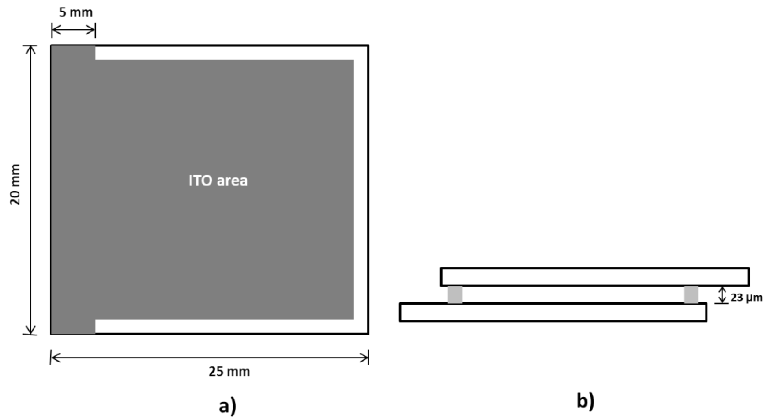
Figure 2.
Schematic representation of a top view (a, left) and lateral view (b, right) of a commercial LC cell model LC2-20.0 provided by Instec Inc (adapted from 18).
Figure 2.
Schematic representation of a top view (a, left) and lateral view (b, right) of a commercial LC cell model LC2-20.0 provided by Instec Inc (adapted from 18).
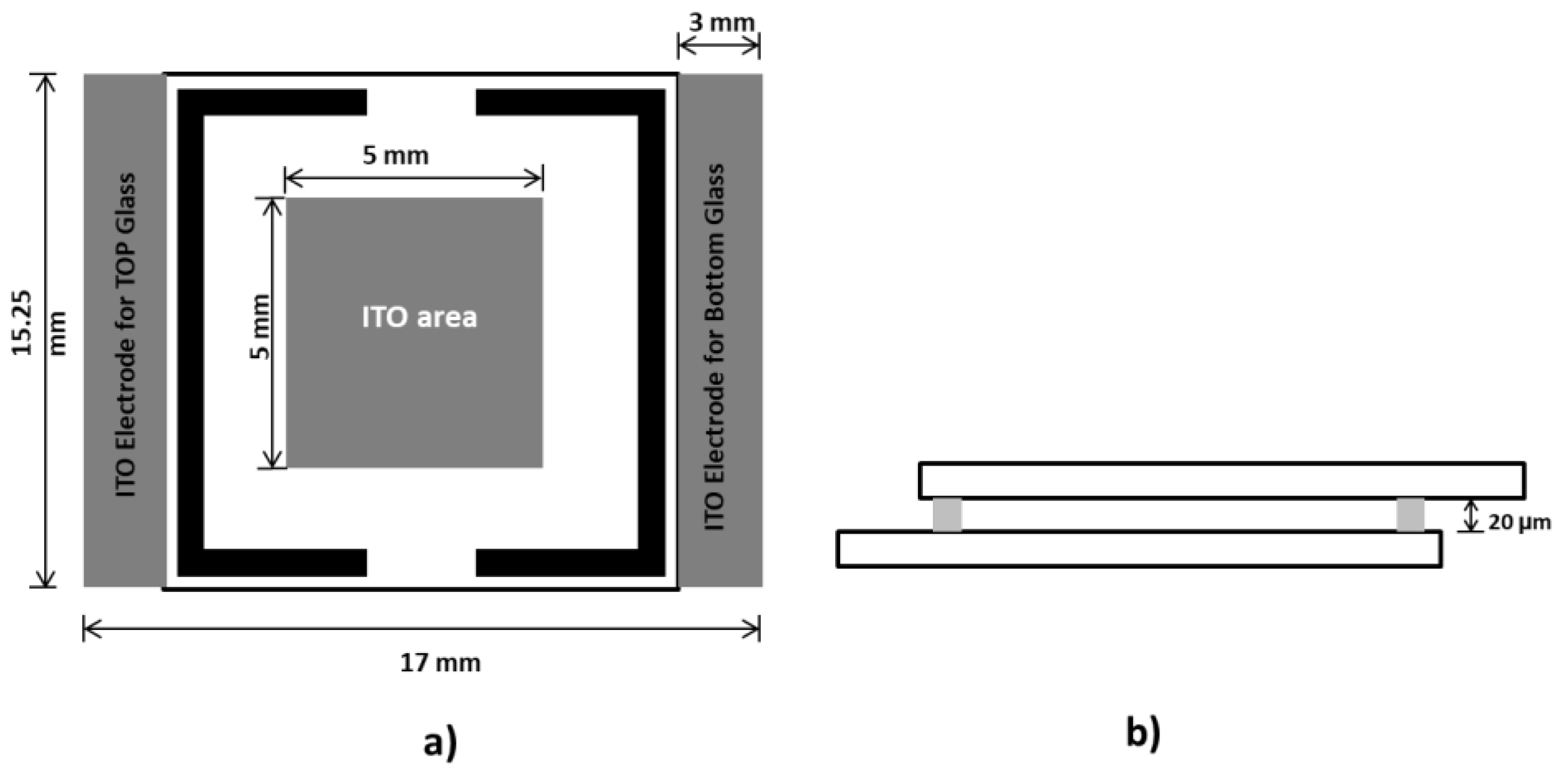
Figure 3.
Conoscopic images of a) homeotropic aligned of E7 and b) homogeneous alignment of E7.
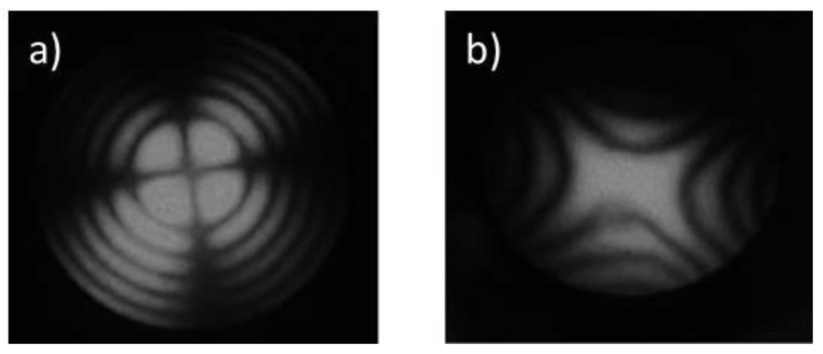
Figure 4.
The effect of the alignment layer on electro-optical (transmittance-electrical field) properties of PDLCs prepared by PEGDM875 (1 wt.% of AIBN)+E7 in a weight ratio of 30/70 (wt.%) and polymerized at 70 ºC, overnight: a) lecithin-PDLC (23 μm thick); b) ITO-PDLC (23 μm thick); c) commercial LC20-PDLC (20 μm thick); d) Perpendicular-PDLC (23 μm thick); e) Parallel-PDLC (23 μm thick) and f) anti-Parallel-PDLC (23 μm thick).
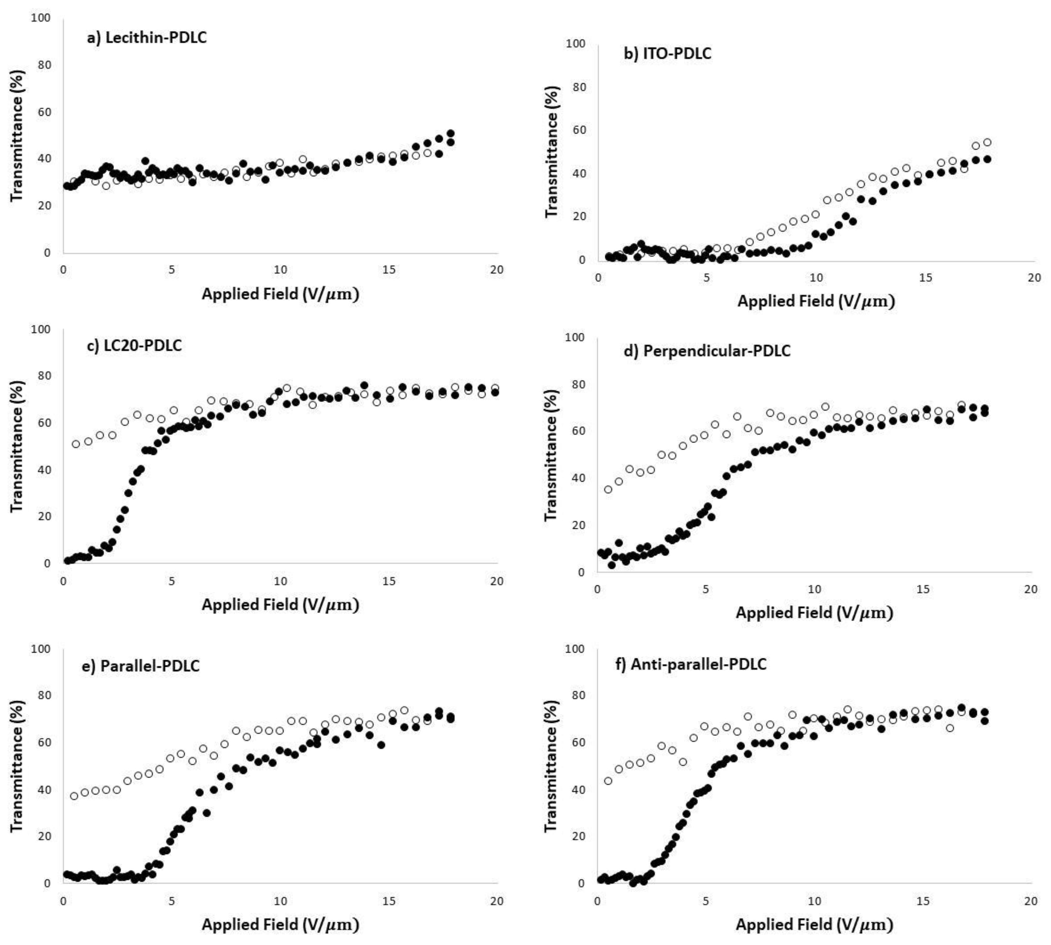
Figure 5.
Schematics of the arrangement of the pre-polymer and liquid crystal in a) homogeneous alignment-PDLC cell; b) homeotropic alignment-PDLC and c) random planar alignment- PDLC cell [16,19].
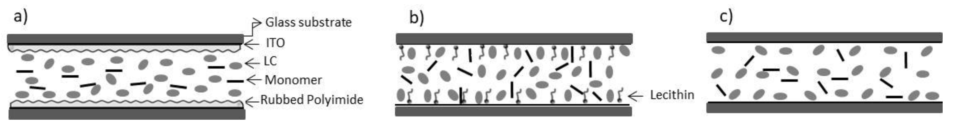
Figure 6.
Top view of a schematic representation of the working principle of optical storage materials in an 8 x 8 passive matrix using PDLC with permanent memory effect units (rows of electrodes on one piece of glass and columns of electrodes on the opposing piece of glass).
Figure 6.
Top view of a schematic representation of the working principle of optical storage materials in an 8 x 8 passive matrix using PDLC with permanent memory effect units (rows of electrodes on one piece of glass and columns of electrodes on the opposing piece of glass).
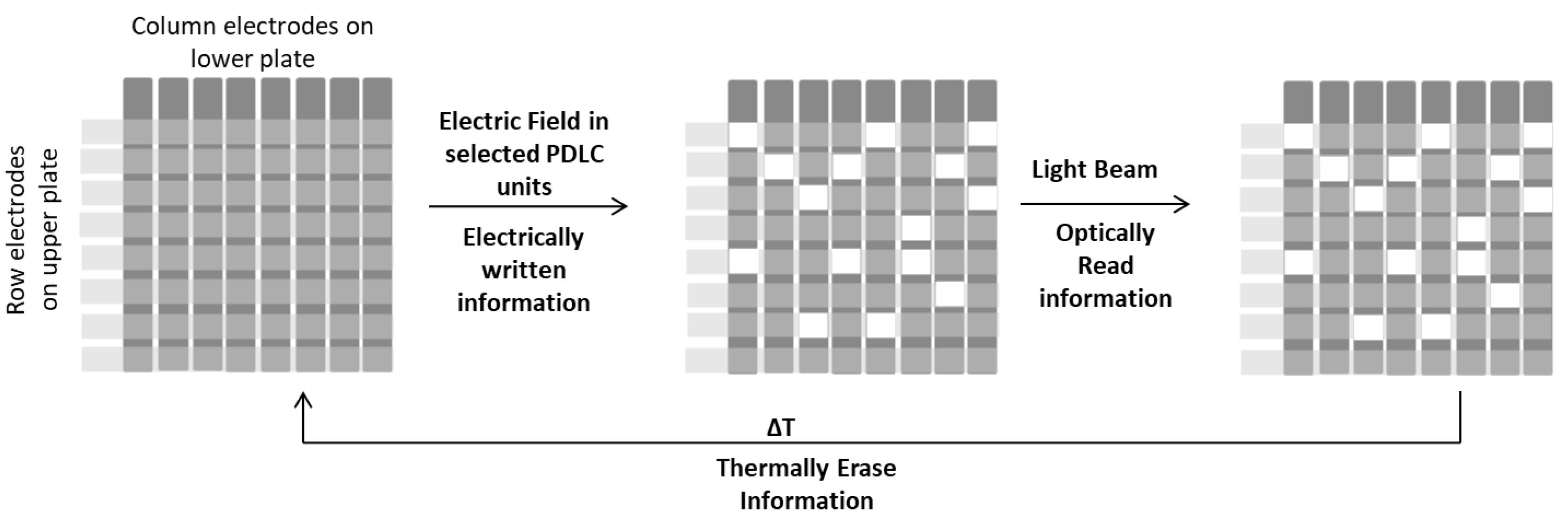
Figure 7.
Image of line-shaped ITO electrodes coated on the glass substrate.
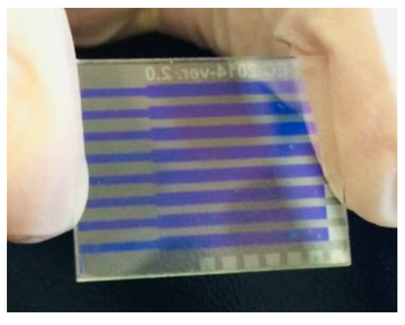
Figure 8.
Schematic illustration of photolithography process to making line-shaped ITO electrodes covered with polyimide.
Figure 8.
Schematic illustration of photolithography process to making line-shaped ITO electrodes covered with polyimide.
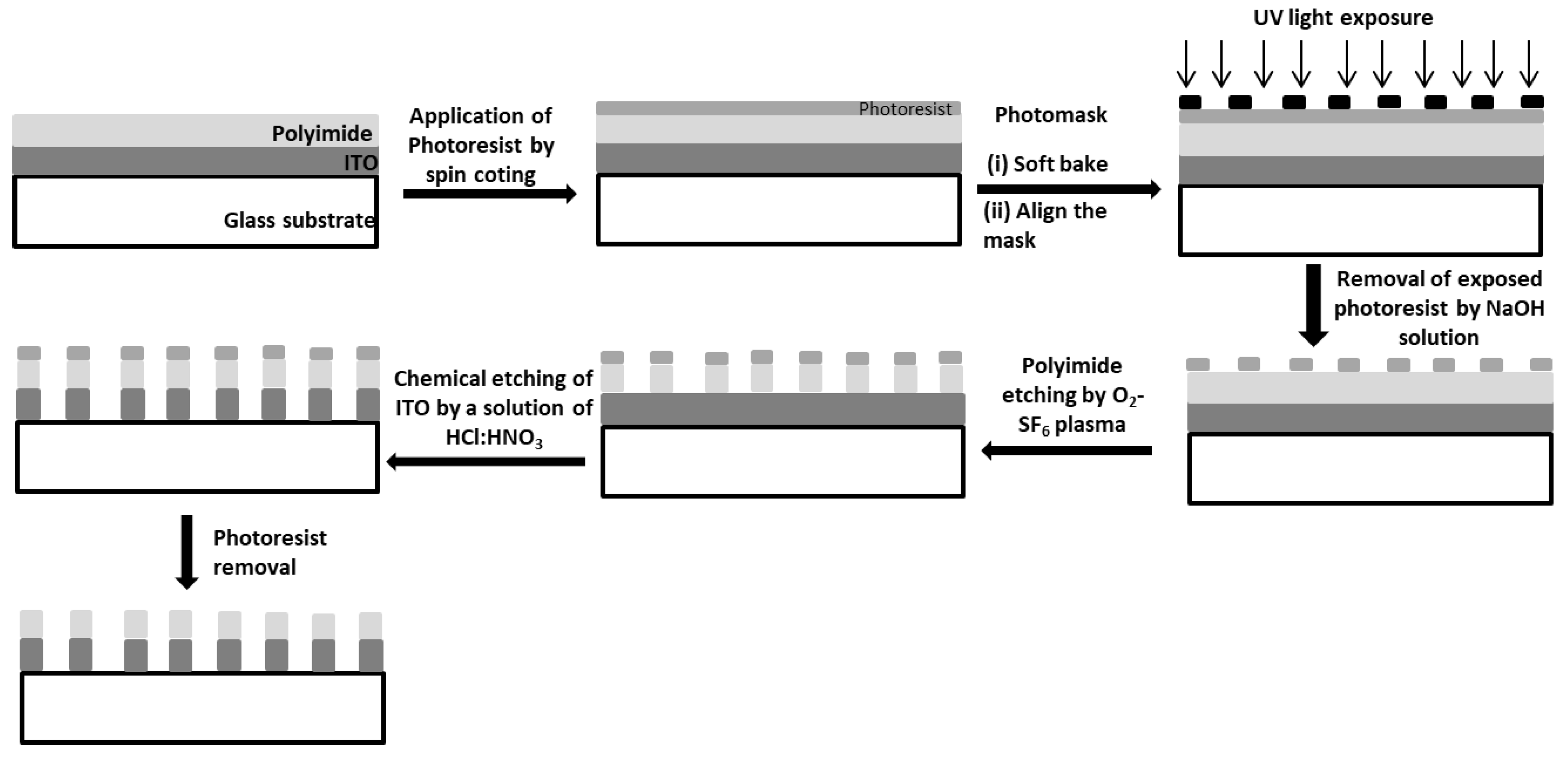
Figure 9.
Schematic illustration of the line thickness measure (a) and line thickness profile (b).
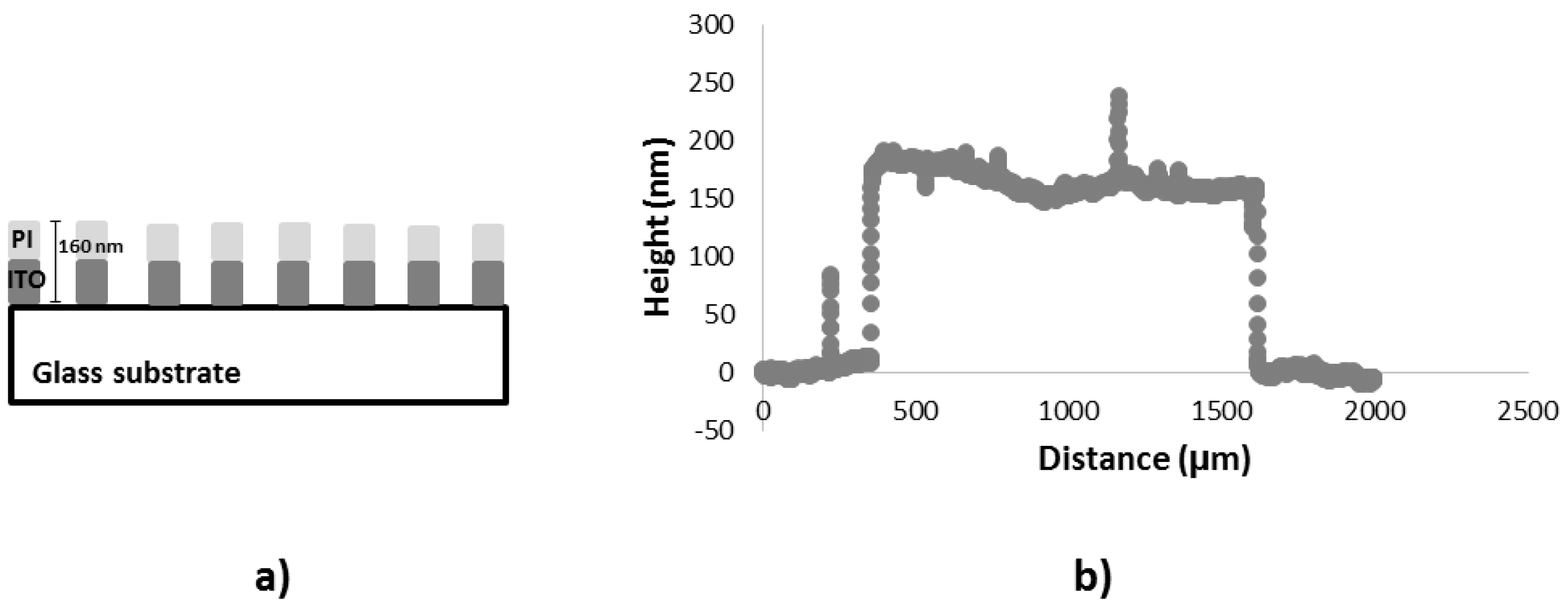
Figure 10.
Photographs of direct observation of the macroscopic performance of PDLC display example in an 8x8 passive matrix: Electrically written at 1 KHz with an applied voltage of a) 0 VRMS, b) 75.3 VRMS, c) 254.4 VRMS and d) after the applied voltage is switched off.
Figure 10.
Photographs of direct observation of the macroscopic performance of PDLC display example in an 8x8 passive matrix: Electrically written at 1 KHz with an applied voltage of a) 0 VRMS, b) 75.3 VRMS, c) 254.4 VRMS and d) after the applied voltage is switched off.
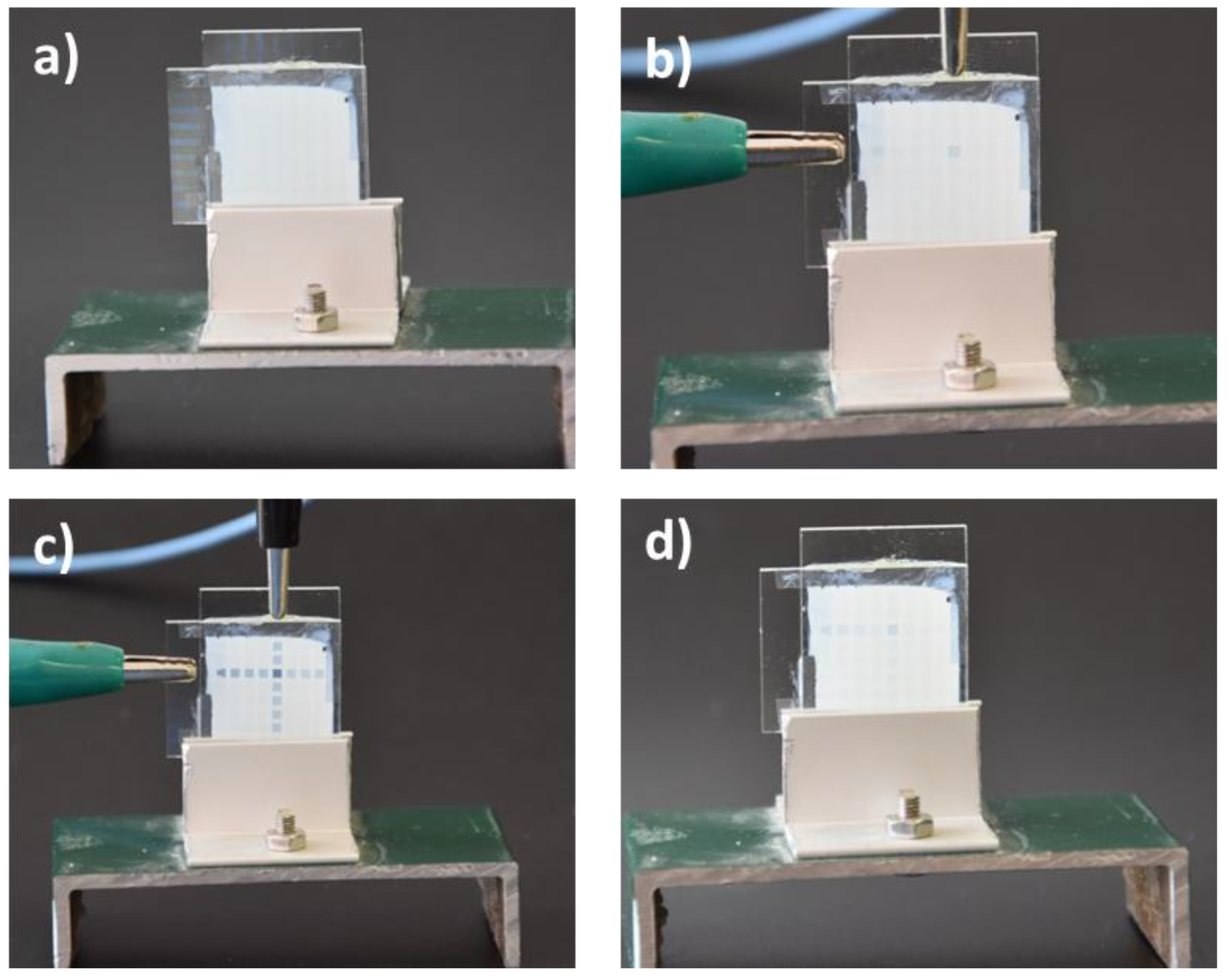
Figure 11.
Photographs of direct observation of the macroscopic performance of PDLC display example in an 8x8 passive matrix, demonstrating the electrically written information effect at 1 KHz with an applied voltage of a) 126.2 VRMS and in b) after the applied voltage is switched off.
Figure 11.
Photographs of direct observation of the macroscopic performance of PDLC display example in an 8x8 passive matrix, demonstrating the electrically written information effect at 1 KHz with an applied voltage of a) 126.2 VRMS and in b) after the applied voltage is switched off.
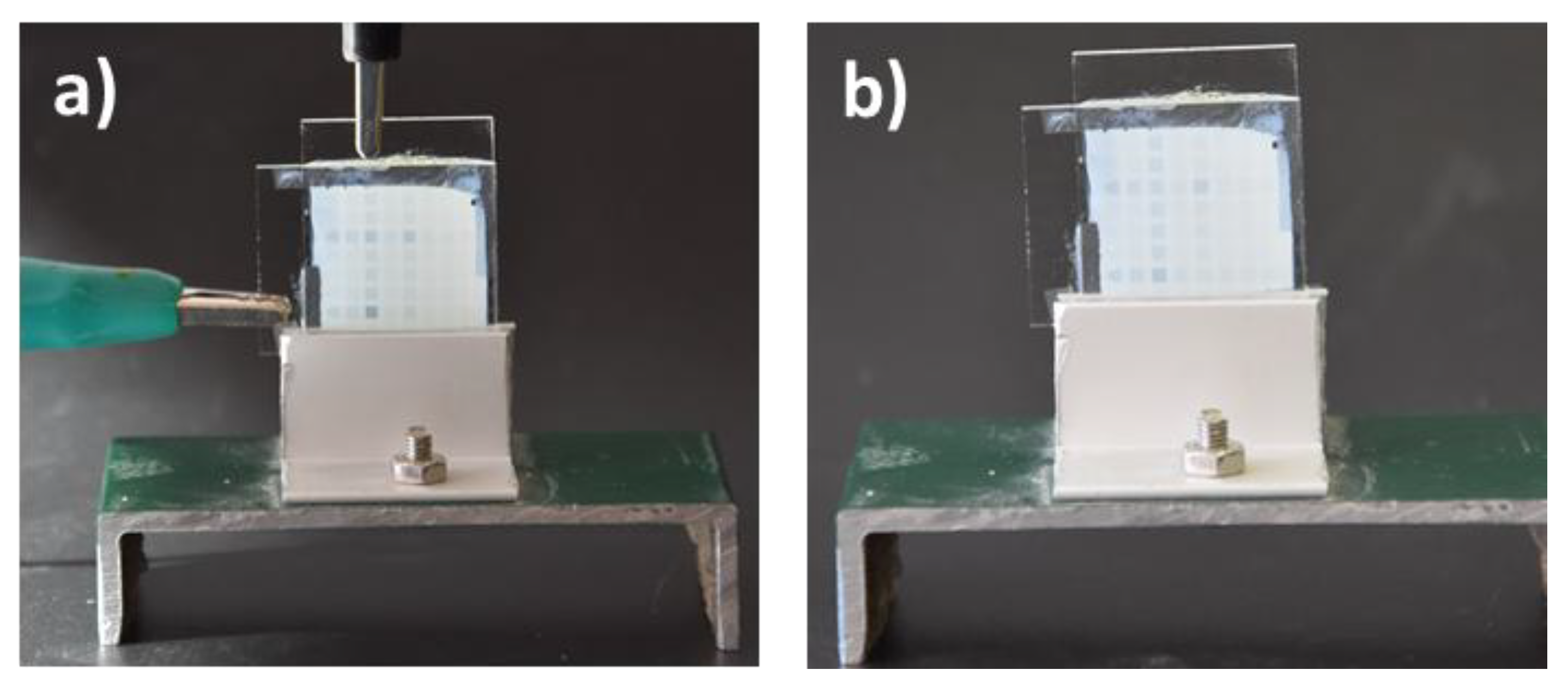

Table 1.
Specifications of passive matrix PDLC device.
| Substrate type | Patterned ITO covered with polyimide coated glass |
| Glass type | soda lime |
| Substrate size (mm2) | 25x25 |
| Active area (mm2) | 21x20 |
| Number of pixels | 8x8 |
| Pixel size (mm2) | 1x1 |
| Gap between pixels (mm) | 0.023 |
Disclaimer/Publisher’s Note: The statements, opinions and data contained in all publications are solely those of the individual author(s) and contributor(s) and not of MDPI and/or the editor(s). MDPI and/or the editor(s) disclaim responsibility for any injury to people or property resulting from any ideas, methods, instructions or products referred to in the content. |
© 2025 by the authors. Licensee MDPI, Basel, Switzerland. This article is an open access article distributed under the terms and conditions of the Creative Commons Attribution (CC BY) license (http://creativecommons.org/licenses/by/4.0/).
Copyright: This open access article is published under a Creative Commons CC BY 4.0 license, which permit the free download, distribution, and reuse, provided that the author and preprint are cited in any reuse.


