Submitted:
15 October 2025
Posted:
16 October 2025
You are already at the latest version
Abstract
Adding P and Sb into InAs produce InAsPSb alloys which offer exclusive opportunities to create optoelectronic devices for operations in the mid-infrared range. These materials are being used to design flexible nano-/micro-electronics. The InAs1-x-yPySbx/n-InAs (GaAs) quantum wells provide strong confinement of electrons and holes. This has changed the carrier capture efficiency, prevented charge leakage and improved performance of devices at higher temperatures. Very few structural and vibrational studies are known for InAs1-x-yPySbx films. Phonons play crucial role for assessing their electronic, and optical traits. Gas source MBE method is used here to prepare high-quality InAs1-x-yPySbx epilayers on n-InAs and/or GaAs substrates. InAs1-x-yPySbx suffer from immiscibility issues when As composition, is less than < 0.4. Results of systematic structural and phonon properties are reported using synchrotron extended X-ray absorption fine structure, Raman scattering and Fourier transform infrared reflectivity. Comprehensive simulations provided valuable information on the nearest-neighbor bond-lengths and vibrational features. These studies can be extended to many other technologically important materials.
Keywords:
InAs1-x(Px)Sbx/n-InAs (GaAs) epilayers
; GS-MBE
; synchrotron extended X-ray absorption fine structure
; Raman scattering
; Fourier transform infrared reflectivity
1. Introduction
Semiconductor based flexible micro-/nano electronic devices has modernized the living standards of peoples worldwide [1,2,3]. Efforts have been made to maintain the ecological balance by conserving natural resources as well as ensuring the safety of both current and future generations. Among III-V compounds, the indium pnictides (InP, InAs, InSb), their ternary InAs1-xSbx(Px) and quaternary InAs1-x-ySbxPy alloys are preferred due to direct band gap alignments [4,5,6,7,8,9,10]. These materials have played important roles for restructuring the landscape of conventional electronic technology. Historical milestones are achieved over the years by preparing epitaxially grown films. Novel digital products have been developed especially the light emitting diodes (LEDs), and laser diodes (LDs), etc. [1,2,3,4,5,6,7,8,9,10] Rapidly evolving innovations also helped reshaping/creating new business opportunities in photonic/optoelectronic industries. Several advanced modules are being integrated into low-powered and ultrahigh speed electronic circuits. These units have been employed to design portable nano-/micro- electronic devices for acquiring solutions in the growing needs of renewable energy, medical diagnostics, and optical communications.
Recently, III-V based photodetectors (PDs) are intensively employed for operations in the mid-wavelength infrared (IR) to long-wavelength IR region of the electromagnetic spectrum. Coupling optical sensors (OSs) with the PDs, and LEDs has enabled detecting absorption lines of pollutants in the environment [11,12]. Compared to solid-state and chemical-based sensing technology, the OSs have offered advantages of miniaturization for quick response -, and real-time detection of biogases in the extended short wavelength IR region. More recently, OSs are integrated in electronics for medical diagnostics (i.e., detecting biological molecules or pathogens in human body), drug analysis, ecological monitoring, and optical communications, etc. Such crucial developments have sparked research interests among scientists and engineers to design efficient electronic devices with low power consumption and high emission intensity [1,2,3,4,5,6,7,8,9,10,11,12].
Depending upon the composition x, the InAs1-x(Px)Sbx ternary alloys exhibit energy bandgap between 0.1 eV–1.34 eV. Significant lattice mismatch in the binary materials [13,14,15,16] leads to strain and intrinsic defects during the epitaxial growth of alloyed epilayers. Despite these constraints, ultrathin InAs1-x(Px)Sbx films are widely used as active medium in optoelectronic devices. Quaternary InAs1-x-ySbxPy alloys are employed as cladding layers for achieving high performance cascade lasers, PDs, and OSs. Due to bandgap tunability, the InAs1-xSbx/InAs1-x-ySbxPy multi-quantum-wells (MQWs) are favored to engineer 3 μm to 12 μm IR detectors. For unipolar carrier transport, the electrons and holes in MQWs can be well separated [17,18,19,20,21,22,23]. This reduces electron-hole (e-h) generation-recombination current and enable device operations at higher temperature, T. The exploitation of InAs1-x(Px)Sbx in active region without requiring aluminum has also helped simplifying the structural designs for fabricating photonic devices.
Irrespective of many positive features, the epitaxial growth of Sb-based materials has been and still is a challenge. Major issues to engineer device structures using InAs(P)Sb are linked to (a) the low vapor pressure of Sb, (b) limitations of kinetically controlled growth regime, (c) inexistence of chemically stable hydrides as precursors, and (d) lack of insulating substrates [24,25,26,27,28,29,30,31,32,33]. Despite these problems, attempts are made for creating alloys and heterostructures by using liquid phase epitaxy (LPE) [34], organo-metallic vapor phase epitaxy (OMVPE) [35,36,37,38,39,40], and molecular beam epitaxy (MBE) techniques [41,42]. Recently improved growth efforts along with superior Sb-based materials, have motivated both engineers and scientists to design bipolar junction transistors (BJTs), LDs, PDs, and OSs. Earlier reports [20,21,22] in InAs/GaSb type-2 SLs (T2SL) have advocated limited value of minority carrier lifetime due to the presence of Ga-related native defects. Now InAs/InAs1-xSbx based T2SL, with longer minority carrier lifetime, has been projected as an alternative system to InAs/GaSb for IR detection. Simple interface of InAs/InAs1-xSbx helps preparing it easily. Moreover, strain-engineered InAs/InAsSb LEDs have demonstrated room temperature (RT) electroluminescence between 2.7 μm - 3.3 μm.
Intrinsic carrier recombination in MQWs is a crucial process. Determined by radiative and Auger recombination, the carrier lifetime in InAs1-xSbx/InAs1-x-ySbxPy is influenced by alloy compositions x, y and strain. Compressive strain can reduce the Auger recombination and increases the radiative recombination rate. This behavior is not universal, it rather depends upon the choice of specific materials and structures. Nonradiative recombination is also a major channel. Possibilities involving Auger recombination exist, where the electron (e) and hole (h) pairs unite by transferring energy and momentum to another carrier rather than emitting photons. In this process, the probability of nonradiative Auger recombination increases exponentially as decreases. This reduces the efficiency of optoelectronic devices like solar cells and LEDs. Despite these issues, many efforts are made for the growth of InAs1-xSbx/InAs1-x-ySbxPy MQWs to design electronic devices for photonic applications [20,21,22]. The material systems with sharp and clean interfaces have advantages of normal incidence, with a broadband absorption.
Despite the successful growth of InAs1-x-ySbxPy/n-InAs or GaAs epilayers, very few attempts are made to study their structural and phonon characteristics. While the structural traits of these materials are influenced by alloy compositions x, y and lattice mismatch, their vibrational properties can have significant impact on the device performance through phonon scattering and thermal transport. For exploring these attributes, a variety of experimental techniques can be adopted. Methods that are frequently employed include Raman scattering spectroscopy (RSS), Fourier transformed infrared (FTIR) reflectivity [43,44,45], high resolution x-ray diffraction (HR-XRD) [41], transmission electron microscopy (TEM) [41], extended x-ray absorption fine structures (EXAFs) [46,47,48,49], electron paramagnetic resonance (EPR) [41], photoluminescence (PL) [41], spectroscopic ellipsometry (SE) [50,51], and electron energy loss (EEL) measurements [41] etc. For InAs1-x-ySbxPy epilayers, limited efforts are made using EXAFS, Raman scattering and FTIR spectroscopy for systematically assessing their structural and vibrational behavior. Meticulous evaluation of these properties is important to optimize device structures for achieving high-performance waveguide modulators, injection lasers, PDs, LDs, and LEDs [1,2,3,4,5,6,7,8,9,10,11,12].
This paper reports the results of our methodical studies (cf. Sec. 2, 2.1–2.4) by carefully analyzing the experimental data for assessing the structural and phonon characteristics of InAs1-x-ySbxPy epilayers. Except for the S4-S9 samples which are prepared on GaAs substrate, most other epilayers are grown on n-InAs by using gas source MBE (GS-MBE). TEM was used earlier to investigate the structural and chemical distributions of atoms [41]. For InAs1-x(P1-x)Sbx alloys the evaluation of Sb composition, x was achieved by performing electron probe microanalysis (EPMA) [41]. Hall studies with van der Pauw methods were conducted at RT on Be- and Si-doped InAs1-x(P1-x)Sbx/GaAs epilayers [41] to appraise their electrical properties. While the optical characteristics were reported by PL measurements [41] limited studies exist, however, on the phonon characteristics using FTIR and Raman scattering spectroscopy [43]. For Raman (cf. Section 3) studies, we have used a Renishaw In Via spectrometer equipped with a 576 × 400-pixel Peltier cooled (−70 ◦C) CCD detector. Besides RSS (cf. Section 4.3), the phonon characteristics are also examined by reflectivity measurements using a Bruker IFS 120 v/S Fourier transformed infrared spectrometer. Numerical simulations of the reflectivity spectra are achieved by adopting a standard methodology of multilayer optics (cf. Section 4.4) within the transfer-matrix-method (TMM) [52]. The structural traits of InAs1-x-ySbxPy epilayers are carefully assessed using the polarization dependent (cf. Section 4.5) synchrotron radiation SR-EXAFS measurements [46,47,48,49]. We have focused our attention on the EXAFS oscillations well above the P K-edge and In K-edge for selectively studying the P- and In-centered local surroundings in InAsPSb. Systematic simulations are performed to comprehend the SR-EXAFS data for attaining average coordination number, and the nearest neighbor In-Sb, In-P, and In-As bond lengths (cf. Section 4.5), etc. Meticulous studies are performed by exploiting IFEFFIT software package consisting of ATOMS, ATHENA, AUTOBK, ARTEMIS programs along with residual space mappings (RSMs) using a valence force field (VFF) model [41] for attaining the distortion energies in InAsPSb alloys. Results of structural and phonon properties on GS-MBE grown InAs1-x-ySbxPy samples are compared/contrasted (cf. Section 4) against the available experimental and theoretical data with concluding remarks presented in Section 5.
2. Experimental Procedures
High quality InAs1-x-ySbxPy/n-InAs (or GaAs) (001) samples used in different experimental investigations are grown by GS-MBE. Most epilayers of ∼1µm thickness are intentionally undoped and prepared by setting the surface temperature of substrate between ~ 470 oC - 480 oC.. Earlier, Hall measurements using van der Pauw method was performed on a few Be- and Si-doped samples for assessing their electrical properties [41]. TEM was also used to investigate the structural and chemical distributions of atoms in InAs1-x(P1-x)Sbx. Phonon and structural characteristics of InAs1-x-ySbxPy epilayers, are systematically appraised by exploiting Raman scattering spectroscopy, FTIR reflectivity, and SR-EXAFS measurements.
2.1. GS-MBE Growth of InAs1-x-ySbxPy Epifilms
Most of the InAs1-x-ySbxPy epilayers of diverse As, P and Sb compositions are grown by gas sourceVG-V80H reactor on n-InAs. Six samples S4-S9 are prepared on GaAs substrate (see Table 1) by carefully setting the temperature of substrates between ~ 470 oC - 480 oC. Pure PH3 gas is injected into the gas cell where the phosphine is cracked at 1000 ◦C for delivering P2. An Sb source is supplied by using an EPI cracking effusion cell. The Sb4 flux from the reservoir zone is further split in the cracking zone at 1050 oC to supply a mixed beam of the Sb2 dimer and Sb monomer. Conventional thermal effusion K-cell is employed with a splitting zone secured at 1000 ◦C to provide the flux flow of the group III indium. The fluxes of Sb and In sources are calibrated by an ion gauge, while the fluxes of As and P sources are controlled via the beam equivalent pressures (BEP) of the arsine and phosphine gases in the manifolds behind the micro-leaks of the gas cells. Cracking zones are set at ~ 1050 ◦C to supply a mixed beam of the Sb, As and Sb2, As2, respectively [41]. All the epilayers are prepared at a growth rate of ~1 μm/hr. In-situ reflection high energy electron diffraction (RHEED) patterns are used for monitoring the surface reconstructions. The compositions of As, P and Sb in InAs1-x-ySbxPy samples [41] determined by a JEOL JXA-8200 electron probe micro-analyzer are reported in Table 1.
2.2. Raman Scattering Spectroscopy
Raman scattering spectroscopy is a powerful and non-destructive technique for characterizing semiconductor materials [43,44,45]. It does not require special preparation of the samples. Different parameters including the intensity, width, peak frequency and polarization provide fruitful information on crystalline quality of the materials. For collecting the Raman scattering spectra (cf. Section 4.3) we have used a Renishaw In Via spectrometer equipped with a 576 × 400-pixel Peltier cooled (−70 ◦C) CCD detector. Spot size of ∼1.6 µm2 was obtained by a 50 × objective lens of a Leica DM2500M compound microscope. Spectral resolution of ∼1 cm−1 is achieved with a 1200-line mm−1 diffraction grating using a 50 µm entrance slit. A 100 mW LD operating at the wavelength of 785 nm (i.e., 1.58 eV which is higher than the bandgap of all the InAs1-x-ySbxPy alloys) is considered here. Power incident on the sample is set at ∼40 mW after allowing optical losses. A holographic notch filter is employed to block the unwanted reflections. Scans between 100 cm−1 to 800 cm−1 are carefully performed at several locations on each sample with a run of 16 accumulations to reduce the effects of noise. An exposure time of 10 s is used to minimize the heating effects while keeping the sample at room temperature. Some local lattice heating is inevitable, however, that resulted in the spectral peak broadening (cf. Section 4.3).
2.3. Infrared Spectroscopy
Besides RSS, we have also examined the phonon characteristics on GS-MBE grown InAs1-x-ySbxPy/n-InAs epilyers by measuring RT infrared reflectivity spectra using a Bruker IFS 120 v/S Fourier transform infrared (FTIR) spectrometer. IR studies are performed on each sample in the frequency range of 50 cm-1 –1000 cm-1 at near-normal incidence (by setting ~ 8o angle of incidence) with a resolution of ~2 cm-1. Valuable information is obtained from the reflectivity measurements. Numerical simulations of reflectivity spectra are achieved by carefully adopting a standard methodology of multilayer optics (cf. Section 4.4) within the transfer-matrix method [52]. Vibrational features of Raman and FTIR spectra in InAs1-x-ySbxPy/n-InAs epilayers have exhibited consistent results indicating a “three-phonon mode” behavior. For samples of higher As composition the InSb-like LO mode is not clearly visible (cf. Section 4.3) in Raman measurements. However, it appeared in the FTIR reflectance spectra. Our results have confirmed that the two methods are complementary to each other.
2.4. Synchroton Radiation Extended X-Ray Absorption Fine Structure
Ever since the availability of broadly tunable sources, the SR-EXAFS spectroscopy has been recognized as one of the most versatile structural characterization tools for studying the local atomic environments in both the crystalline and amorphous materials [46,47,48,49]. Information offered by SR-EXAFS spectra in different materials has included the assessment of average interatomic distances and number of chemical identities of neighboring atoms between 1.4 Å – 10 Å. On several GS-MBE grown InAs1-x-ySbxPy samples, we have collected the P K-edge, and In K-edge polarization dependent SR-EXAFS spectra in the fluorescence yield mode (cf. Section 4.5) using 16 A and 01 C beamlines at the National Synchrotron Radiation Research Center (NSRRC) in Hsinchu, Taiwan. In these measurements, the radiation fluxes were set at 3 × 10¹¹ photons/sec on a spot size of 0.5 × 0.4 mm and 3 × 10¹⁰ photons/sec on a spot size of 0.9 × 0.2 mm, respectively. At the 16 A beamline, a double crystal monochromator equipped with a Si (111) crystal and Ni-coated mirrors was used, while at the 01 C beamline, a monochromator with Pt-coated mirror was employed. A filter between the sample and detector window was inserted to help reduce the noise from scattering for improving the spectral quality. The fluorescence emitted from each sample was carefully evaluated with an argon filled Stern-Heald-Lytle type detector. The In K-edge EXAFS spectra of InAs1-x-ySbxPy epilayers are expected to exhibit signals (cf. Section 4.5) from In-P, In-As, and In-Sb bonds.
3. Theoretical Background
Vibrational characteristics of zincblende (zb) InP, InAs, and InSb materials can be assessed theoretically by studying their lattice dynamics. While indium pnictides share structural similarities, however, different atomic masses of P, As, and Sb have resulted in distinct phonon dispersions. In III-V semiconductors, the lattice dynamics has been extensively studied (cf. Section 3.1) by experimental [53,54,55,56] and theoretical methods [57,58]. Inelastic neutron scattering (INS) spectroscopy [53,54,55,56] provides the direct measurements of detailed phonon dispersion curves throughout the Brillouin zone (BZ).
3.1. Lattice Dynamics of InP, InAs, and InSb
Comparison of lattice dynamics [57,58] for indium pnictides by realistic lattice dynamical studies has revealed trends based on two important aspects: (a) increase of atomic mass of anion atoms (P→ As→ Sb), and (b) decrease of ionic character between their bonds. Compared to InAs and InSb, the optical phonon frequencies are highest for InP due to lighter P atom. Large gap between acoustic and optical phonon branches exists in InP than InAs. Due to heavier Sb, smaller gap is noticed in InSb. These traits have played important roles for analyzing the experimental FTIR reflectivity and Raman scattering spectroscopy data on InAs1-x-ySbxPy/n-InAs epilayers (see Section 4.3 and Section 4.4).
3.2. Analyzing IR Spectra of InAs1-x-ySbxPy Epilayers
Transfer matrix method is used for simulating the FTIR reflectivity spectrum of epitaxially grown heterostructures. The approach is based on propagation of electromagnetic waves into a stack of layers [52]. In epitaxially grown structures, TMM includes the effects of absorption, dispersion, as well as constructive and/or destructive interferences from multiple reflections within the layers. The method has been successfully used to comprehend thickness-, and composition-dependent IR spectra of different multilayer structures [52]. In Section 4.4 we have employed TMM for accurately assessing the observed FTIR reflectivity phonon features in GS-MBE grown InAs1-x-ySbxPy/n-InAs films.
3.3. Characterization of EXAFS Data on InAs1-x-ySbxPy Epilayers
Although, the SR-EXAFS at P K-edge and In K-edge is a specialized approach for determining local atomic environment around P- and In-centered atoms in InAs1-x-ySbxPy /GaAs epilayers the method, however, presents many challenges. In characterizing structural properties of complex systems, the EXAFS spectra provide valuable insights into bonding, coordination number, and neighboring atomic species [46,47,48,49]. The SR-EXAFS is effectively used for studying the short-range properties of InAsPSb which otherwise cannot be revealed by conventional methods. Energy required to excite a P K-edge (In K-edge) electron is in the X-ray regime, specifically at ~ 2150 eV (~ 27,940 eV). Working with soft X-rays introduces experimental challenges not present, in the hard X-ray EXAFS. Synchrotron radiation x-ray absorption spectral measurements are carried out at RT with spectra normalized to the intensity Io of the incident photon flux (cf. Section 4.5).
3.3.1. Distortion Energy
Distortion energy in InAs1-x-ySbxPy epilayers grown by GS-MBE on GaAs is caused by mismatch between the native (unstrained) and strained bond lengths of In-As, In-P, In-Sb. Comprehending distortion energy in terms of the changes in bond length is difficult to relate by a simple analytical expression. Distortion energy depends on the total energy of InAs1-x-ySbxPy, their bond lengths and compositions, x, y. Careful analysis of EXAFS data, with simulations of RSMs along with the average vertical az to horizontal lattice constant axy ratios are used for articulating the residual strain. A VFF model [59,60] is employed to express distortion energy with az/axy of the InAsPSb supercells. Consistent (cf. Section 4.5) with EXAFS data, the In-P, In-As and In-Sb bond lengths are found closer to those of the bulk binary materials. Strain is attributed to the non-vanishing distortion energy resulting from the difference in bond lengths between InP, InAs and InSb bonds.
4. Results and Discussions
Quaternary III-V alloy semiconductors InAs1-x-ySbxPy are commonly used as detectors and emitters in the MWIR optoelectronics [1,2,3,4,5,6,7,8,9,10,11,12]. Basic traits of these alloys include tunable bandgaps and lattice constant a which depend on their specific compositions, x, y. These fundamental features are required to design electronic devices for various applications. InAs1-x-ySbxPy involves three binary InP, InAs and InSb compounds of zb crystal structures. Growth of high-quality quaternary alloys can be difficult due to potential challenges of mismatch with substrates, compositional non-uniformity, and optimizing growth kinetics [4,5,6,7,8,9,10]. Lattice constant of quaternary InAs1-x-ySbxPy alloy can be adjusted by varying x, y. Techniques like step-graded or metamorphic buffer layers are also suggested to overcome the issues of lattice mismatch [1,2,3,4,5,6,7,8,9,10,11,12]. These developments have allowed flexibility in device design by preparing high-quality epilayers on lattice-matched InAs and/or GaAs substrates [35,36,37,38,39,40,41,42]. Such epilayers have been employed in strain-engineered heterostructures. Tensile-strained barriers are used compensating the high compressive strain in InAs1-xSbx/InAs1-x-ySbxPy QWs. Larger bandgap InAs1-x-ySbxPy barrier relative to active InAs1-xSbx layer is known for enhancing the carrier confinement. This choice of QW in LEDs has also led [29,30,31,32,33] to higher carrier extraction efficiency with improved quantum efficiency, and reduced efficiency droop.
4.1. Crystalline and Structural Properties
In Figure 1a) we have displayed the lattice constant a (Å) versus electron energy bandgap of several III-V compound semiconductors. Figure 1b) shows the calculated composition planes along with spinodal curves for different growth temperatures in the quaternary InAs1-x-ySbxPy alloys.
Open blue colored circles in Figure 1 b) represent the composition, determined by EPMA [41] for several GS-MBE grown samples (see Table 1). Composition plane, along with spinodal curves are calculated using delta lattice parameter (DLP) model [61]. Results are displayed for the growth temperatures of 400 oC, 600 oC, 800 oC and 1000 oC using green, blue, violet and black color lines, respectively. Calculations of spinodal curves assume thermodynamic equilibrium conditions. However, GS-MBE approach is generally thought to be far from the thermodynamic equilibrium. Thus, epitaxial growth kinetics has played important role in determining the materials’ structural characteristics. Several researchers have pointed out that as the depositing layer is slightly mismatched to the substrate, the effect of resulting coherent strain may decrease the critical, T of the spinodal point [41]. This allows meta-stable growth in the immiscibility region as shown in Figure 1 b). One may note that the six samples with low composition of arsenic are grown inside the immiscibility region. The lattice constant of InAs is 6.0583 Å, and the calculated lattice mismatch of the grown layers is found to be less than 0.4%, with only those samples within the immiscibility region having a lattice constant smaller than that of the InAs.
4.2. Comparative Lattice Dynamics of Indium Pnictides
Lattice dynamics of indium pnictides has been extensively studied by using experimental (e., IR and, Raman scattering spectroscopy) and theoretical methods [53,54,55,56,57,58]. Inelastic neutron scattering (INS) spectroscopy [54,55,56] is one of the most accurate techniques for measuring phonon dispersions of different materials including semiconductors. Experimental data on lattice dynamics has encouraged researchers to develop theoretical methods by exploiting both the first principles and phenomenological models. Ab initio studies are used for determining the atomic-scale vibrational properties of materials from their basic physical traits without including experimental data or empirical parameters. Such calculations have employed density functional theory (DFT) to solve the Schrödinger equation for accomplishing accurate descriptions of , and thermodynamic properties [57,58]. For InP, InAs and InSb, many ab initio calculations have employed commercial packages of ABINIT software and Quantum-Espresso programs for predicting their phonon and electronic characteristics [58]. Here, we have used a realistic rigid-ion-model (RIM) [57] and reported our calculations of (see Figure 2 ac)) for indium pnictides. Theoretical results are compared/contrasted reasonably well with the existing INS, RSS [53,54,55,56] data, and ab initio simulations [58].
Perusal of Figure 2 ac) show identical features of phonon dispersions for InP, InAs, and InSb materials because of their common zb structures. Results also revealed significant differences due to the variation of group-V anion P, As, Sb masses. Increasing mass ratio of the two atoms have demonstrated several key trends across the InP→ InAs → InSb series: (i) InP has the highest phonon frequencies of longitudinal optical LO () and transverse optical TO () modes with wider separation between its acoustic and optical branches, (ii) in InAs the phonon mode frequencies are lower than InP due to heavier As atom, and (iii) InSb showed the lowestphonon values than InP and InAs due to the involvement of heaviest mass of Sb.
4.3. Composition Dependent Raman Scattering Spectra
Raman scattering is a powerful and non-destructive method. It has been frequently used for exploring the vibrational features of both simple and complex ionic materials [43,44,45]. In the ternary and/or quaternary alloys, the RSS is employed for characterizing the composition dependent phonon modes. In epitaxially grown heterostructures, the analysis of Raman scattering data has helped assessing the crucial information on their structural, interfacial, strain, electronic transitions, confinement of acoustic phonons, as well as the photoexcited e-h plasmas for creating coupled-plasmon LO modes, [43,44,45], etc.
In Figure 3, we have displayed our RT results of the Raman scattering studies performed on eight different GS-MBE grown samples in the backscattering geometry. In this configuration, one would expect observing only the modes as the phonons are forbidden. The observation of both modes in InAs1-x-ySbxPy alloys are possibly caused by disorder. Results on different InAs1-x-ySbxPy/n-InAs samples with increasing values of As have provided useful information on: (a) the specific compositions of constituent materials, (b) disorder induced modes, and (c) lattice mismatch-induced strain between epilayers and substrates. In Figure 3, the vibrational features with shifts of Raman peaks of InP-, InAs-, and InSb-like modes are markedly visible. In InAs1-x-ySbxPy/n-InAs the observed phonon modes along with the presence of additional disorder-related broad bands are used for monitoring their overall crystalline quality, strain, and composition.
Raman scattering results in InAs1-x-ySbxPy/n-InAs epilayers (see Figure 3) have revealed InAs-like and modes (~218 cm-1) and (~238 cm-1)] when the As composition is increased between 0.219 to 0.98. As a guide to the eye, the InAs-type phonons are shown by using the orange and sky-blue curved lines. In samples with P composition between 0.264 to 0.725, the observed InP-like (~307 cm-1) and (~345 cm-1) modes are indicated by green and brown color arrows or curved lines. In InAs1-x-ySbxPy/n-InAs epilayers with Sb composition between 0.214 to 0.234, our Raman scattering measurements have identified a prominent InSb-like (~182 cm-1) phonon peak shown by a violet arrow or curved line. A broad phonon feature shown by black colored arrows near (~275 cm-1) that appeared between InAs- and InP- like modes is assigned as a disorder-activated optical phonon band within the immiscibility region [41] or as a InAs:P local vibrational mode. The ability of examining strain and disorder in GS-MBE grown samples can be valuable for evaluating the performance of photonic devices when they are integrated in MQWs. Clearly, the Raman scattering results have confirmed the prospects of “three-phonon-mode behavior”. The assignments of InP, InAs and InSb-like optical phonons are consistent and fully supported by our FTIR reflectivity, RIM results of phonon dispersions (see Figure 2 ac)) and other Raman scattering data (see: Table 2).
4.4. Composition Dependent Infrared Spectra
Very few measurements are known using FTIR reflectivity spectroscopy to comprehend the vibrational characteristics in InAs1-x-ySbxPy quaternary alloys. In the related III-V ternary AB1-xCx alloys, several IR and RSS experiments have provided strong basis of identifying phonon features in terms of their binary AB, AC compounds. Following Chang and Mitra [62], one can classify the one-phonon-mode behavior in GaxIn1-xP and two-phonon-mode behavior in InAs1-xPx(Sbx) ternary alloys. In the quaternary InAs1-x-ySbxPy compounds, however, the vibrational feature has not been firmly confirmed. Our FTIR measurements on GS-MBE grown InAs1-x-ySbxPy/n-InAs epilayers have revealed multiple phonon features with distinct vibrational bands. These characteristics are clearly linked to three In-P, In-As, In-Sb like bonds of the binary zb indium pnictides.
In Figure 4 a-f) we have reported our infrared reflectivity spectra on several GS-MBE grown InAs1-x-ySbxPy/n-InAs samples having different alloy compositions x, y. The experimental results recorded at RT, are displayed by using full blue color lines. The FTIR spectra are contrasted against our theoretical fit achieved by using TMM [52]. The simulated results are indicated by red color open squares. Clearly our experimental and theoretical results have confirmed the observed frequency shifts, influenced by In-P, In-As, In-Sb like phonon energies including the disorder activated modes. Consistent with the Raman scattering spectroscopy, the FTIR reflectivity results on samples with explicit alloy compositions x, y has provided a reasonably good theoretical fit. Undoubtedly, the FTIR spectra of InAs1-x-ySbxPy alloys have demonstrated a “three-phonon-mode” behavior.
4.4.1. Three Phonon Mode Behavior
Distinct optical phonon peaks corresponding to In-P, In-As, and In-Sb-like lattice vibrations are observed in Raman scattering (cf. Section 4.3) spectroscopy, as well as FTIR reflectivity measurements (cf. Section 4.4). Analyses of these results using RIM calculations of lattice dynamics have revealed InP, InAs and InSb like phonons along with alloys’ structural disorder modes (cf. Figure 5). Unlike III-V ternary alloys including Ga1-xInxP and InAs1-xSbx(Px) which displayed either one-phonon mode and two-mode behavior, respectively – in InAs1-x-ySbxPy alloys our studies have exhibited “three-mode” behavior of different bond types by observing their appropriate optical phonon peaks.
Summarizing the vibrational results on epitaxially grown InAs1-x-ySbxPy/n-InAs specimens, we have noticed that Raman scattering spectroscopy and FTIR reflectivity measurements are complementary to each. Theoretical analyses of experimental data have confirmed that: (a) InP-like modes are the most stable features across a wide range of P composition, (b) InAs-like phonons appear at higher As concentration, and (c) InSb-like modes are noticed only at higher Sb composition.
4.5. Composition Dependent SR-EXAFS Spectra
SR-EXAFS spectroscopy is a powerful technique commonly used for analyzing the local atomic structure of different materials [46,47,48,49]. It is an element-specific approach usually employed for probing atomic environment around the absorbing atom. When applied to InAs1-x-ySbxPy/GaAs epilayers, the SR-EXAFS spectra are extremely sensitive to the alloy compositions, x, y. Careful analysis of EXAFS data for such materials can provide valuable information of their bond lengths, coordination numbers, and local disorder.
In exploring polarization dependent SR-EXAFS data, we have studied experimental oscillations well above the P K-edge and In K-edge, respectively. These results helped us selectively studying the P- and In-centered local surroundings of GS-MBE grown samples. When the core-level electron is excited by incident x-ray, the resulting photoelectron scatters off the surrounding neighboring atoms. Interference patterns of such scattered photoelectrons with outgoing wave provided oscillations in the x-ray absorption coefficient μ [63]. For InAsPSb, the EXAFS spectra without double crystal monochromator (DCM) energy calibrations can cause systematic errors, rendering unreliable data (cf. Section 4.5.2).
Analysis of EXAFS oscillations via the Fourier transformation, have exhibited radial distribution χ(E) functions. These functions offer estimating distances and number of neighboring atoms from the absorbing atom. One can express the energy-dependent χ(E) using x-ray absorption coefficient μ, where the single scattering mechanism dominates. The function χ(E) may be evaluated by using the following relationship: [63]
In Equation (1), the term is the experimentally observed absorption coefficient; (E) is a smooth background function representing the x-ray absorption by an isolated atom; is the measured jump (‘edge-step’) in the absorption at the threshold energy (i.e., the binding energy of the core-level electron). In InAs1-x-ySbxPy epilayers, the x-ray absorption spectral coefficient μ as a function of E has revealed the sharp rise in intensities at the P K-edge and In K-edge, respectively. The absorption results initiated almost step-like functions with weak oscillatory wiggles observed beyond several hundred eV above the edge. The region closer to absorption edge is often dominated by the strong scattering processes including the local atomic resonances.
Since the EXAFS data is best described by the wave-like behavior of the photoelectron created in the x-ray absorption process, it has been a common practice to exploit the EXBACK program to convert the x-ray energy E to wavenumber of the photoelectron. This has helped us evaluating the χ(k) results as a function of from the raw data. Thus, we focused our attention on the region of EXAFS oscillations covering the x-ray photon energy E from nearly tens of eV above the absorption edge. The results are carefully analyzed for extracting the structural characteristics.
From the observed P K-edge and In K-edge EXAFS oscillations including the non-Gaussian disorder for the InAs1-x-ySbxPy materials, χ(k) is expressed in the single scattering and plane wave approximations: [63]
where, is the electron mean free path; is the atomic backscattering amplitude; the angular bracket < > is the thermal average; is the net phase shift; is an amplitude reduction factor due to many body effect; N is the coordination number; and R is the instantaneous bond length between the backscattering and absorbing atoms. From Eq. (2), it is obvious that one requires χ(k) – the key quantity for experimental analysis of the EXAFS data. Extraction of the EXAFS modulation function χ(k) is achieved from the raw absorption data (cf. Sec. 2.4) following the standard procedures described elsewhere [63].
In Figure 6 ab) we have reported the results of Fourier transformed EXAFS spectra χ(R) versus R between 0 to 6 Å in the P K-edge and In K-edge, respectively for the GS-MBE grown samples of different compositions x, y.
To fit the experimental EXAFS data of χ(R) (cf. Figure 6 ab)), we have adopted appropriate programs from the IFEFFIT package. These programs consist of ATOMS, ATHENA, AUTOBK, ARTEMIS that helped us converting the oscillating features of absorption coefficients to the Fourier transform spectra. The AUTOBK program [63] was exploited for removing the background contributions from the k-space signals. The perusal of Figure 6 a) in the P K-edge spectra for InAs1-x-ySbxPy samples has clearly revealed In-P bond lengths exhibiting nearly identical values, despite the changes in P compositions. These values of In-P bond lengths are closer to the bond length of bulk InP binary material [48]. For larger P compositions three distinct peaks at R ~2.1 Å, R ~3.9 Å, and R ~ 4.6 Å are linked representing to the scattering from first (P), second (In), and third (P) nearest neighbors (NNs), respectively [48]. Technically, the In K-edge EXAFS spectra are expected for providing the signals from In-P, In-Sb, and In-As bonds. From Figure 6 b), one can notice that for InAs1-x-ySbxPy samples with low As compositions, separate peaks representing to In-P [48] and In-Sb ~ 2.79 Å [49] bonds are evident. By increasing As composition, the peaks are spotted gradually merging into the In-As ~ 2.60 Å signal [46].
4.5.1. Valence Force Field Model Analysis of SR-EXAFS Spectra
To further explicate the EXAFS spectra, accurate numerical simulations are necessary. In InAs1-x-ySbxPy alloys, theoretical methods must account for the four atomic species forming In-P, In-As and In-Sb bonds, as well as compositions and carefully varying the bond lengths and bond angles. Here, we have adopted a VFF model to calculate the bond lengths which includes both the bond-stretching and bond-bending terms. Calculations are performed for the atomic positions in the InAs1-x-ySbxPy alloys of the In-centered configurations. Here, we have carefully selected the group III atom and used random numbers to consider the position of each group V atom in the supercell. The numbers of P, As and Sb atoms were chosen according to their mole fractions determined from EPMA. To fit the EXAFS signals we have meticulously adopted the ARTEMIS codes [63]. Choice of these arrangements are linked to the values of the bond-lengths close to In-P estimated in the EXAFS spectra.
Atomic positions in InAs1-x-ySbxPy alloys are carefully estimated by minimizing the total energy. Once the atomic positions with minimized energies are achieved by using a VFF– the output can be carefully exploited for simulating the reciprocal space maps of the quaternary alloys [59,60]. Modeling of RSMs is a sophisticated approach for predicting the atomic structure by linking it to the observed HR-XRD patterns in the quaternary alloys. We have used RSMs to inspect the lattice relaxation of InAsPSb grown on GaAs substrates to extract vertical az and horizontal axy lattice constants (see: Table 3). For details of this approach, we refer to one of our earlier papers [41] epilayers. The ratio az/axy describes the deformation of the crystal unit cell relative to its relaxed, unstrained state.
4.5.2. Calibrated SR-EXAFS Spectra
For complex alloy systems, the measurement of EXAFS spectra without DCM energy calibrations can introduce systematic errors, rendering the resulting data unreliable for quantitative analysis. The DCM energy calibration is an essential step to ensure that the detected absorption features correspond to the correct X-ray energies, which is critical for the structural analysis of InAsPSb alloys. Hence, the EXAFS data for materials must have their energy calibrations done before performing the quantitative fits. This is a critical prerequisite for accurate analysis, not an optional post-step. In Figure 7 ab) we have reported our P K-edge EXAFS spectral results on the GS-MBE InAsPSb samples before and after the DCM energy calibration.
Careful fitting procedure of EXAFS data (Figure 7 ab) has provided structural parameters (see: Table 4). These are linked to the definition of absorption edge energy [63].
In Table 4, we have listed the necessary EXAFS fitting parameters evaluated carefully before and after DCM energy calibrations. These parameters (cf. Section 4.5) include the amplitude reduction factor , relative square displacements , coordination number N, bond length R, and ΔR, etc. For InAs1-x-ySbxPy/GaAs epilayers, we have compared in Figure 8 the simulated bond length variation versus As composition. The displayed results include our meticulous analysis of the EXAFS data (Table 4) as well as the simulations of bond lengths from the VFF model. Clearly, the perusal of Figure 8 has indicated the alloy bond lengths which are closer to their values in the binary materials. The consistency of experimental and simulated results has also supported the validity of the two approaches.
4.5.3. Internal Distortion Energy in InAs1-x-yPySbx/n-InAs Epilayers
In Figure 9 a) we have plotted the simulated results of distortion energy as a function of az/axy for the GS-MBE grown InAs1-x-yPySbx/GaAs samples (Table 4). Figure 9 b) denotes the energy differences by using the energy at az/axy = 1 as a reference. In fact, we fixed the az/axy ratio and find the lowest distortion energy for each specified ratio for generating six curves displayed in Figure 9(a). The strain energy curves in Figure 9b) are calculated from the curves in Figure 9a) by subtracting the distortion energy with az/axy = 1 from each distortion energy (with different az/axy). Again, we have noticed that the strain energy curves coincide the results calculated using the elastic constants of the alloys and their values are much lower than the distortion energies. This result clearly suggests that the internal distortion is much stronger than the stress resulting from the lattice mismatch. Obviously, it supports our earlier argument that the internal distribution hinders the lattice relaxation. Thermal mismatch between InAsPSb and InAs substrate causes a thermal strain. However, its level being < 0.1 % is certainly negligeable.
5. Concluding Remarks
Epitaxial growth of different InAsPSb, AlGaAsSb and InGaAsSb ultrathin films has played valuable roles for designing high-performance, low-power integrated circuits, inter-band cascade lasers [65] and next-generation flexible and portable electronic devices [1,2,3,4,5,6,7,8,9,10,11,12]. Optimum performance of various device structures, involving these epilayers is contingent on their structural and lattice dynamical characteristics. Vibrational and structural behavior is generally influenced by the film thickness, alloy composition, interfacial strain and epitaxial growth conditions, etc. [8,9,10] In the nanostructured epilayers, the interaction of phonons with intrinsic and/or extrinsic charge carriers has been and still is a major issue for evaluating their role in thermal management, thermoelectric energy conversion, and thermal insulation of different electronic devices. Lack of such important basic traits has encouraged crystal growers to select appropriately the quaternary alloyed III-V semiconductor materials and meticulously prepare them epitaxially on different substrates viz., InAs, GaSb, GaAs and Si, etc. [1,2,3,4,5,6,7,8,9,10,11,12] Attempts are made by fine-tuning their structural and phonon properties for achieving specific electronic and optical responses in various electronic devices. Good quality InAs1-x-yPySbx/n-InAs (GaAs) samples of nearly ~1 mm thick films are successfully grown by GS-MBE technique. Systematic experimental measurements are performed on these epilayers by exploiting Raman scattering spectroscopy (cf. Section 4.3), high resolution FTIR reflectivity (cf. Section 4.4) and SR-EXAFS (cf. Section 4.5) techniques. These methods have played valuable roles for comprehending their vibrational and structural characteristics.
Combining the experimental reflectivity data with a standard methodology of multilayer optics using TMM approach has helped us assessing the refractive index and extinction coefficient for both the epilayers and substrate. The values of and are used for modelling the reflectivity spectra to achieve a very good agreement with the experimental data. The FTIR reflectivity results have complemented the Raman scattering data and provided a complete picture of phonon characteristics in the InAs1-x-yPySbx /n-InAs samples. Composition-dependent phonon shifts, linewidths and Raman intensity peaks offered valuable information about the crystalline quality of InAs1-x-yPySbx epilayers. While sharp and intense peaks have indicated the high-quality materials, the broadened and/or weak intensity features pointed out either to the structural defects and/or disorder in the GS-MBE grown samples (cf. Section 4.3). Most importantly, both the Raman scattering and FTIR reflectivity measurements have complemented each other by confirming a “three-phonon-mode” behavior in InAs1-x-yPySbx alloys. Vibrational frequencies of InAs-like, InSb-like, and InP-like modes are observed in these samples, while disorder-related dynamical features are noticed within and/or near the miscibility gap region. Defects previously described in the GS-MBE-grown InPSb epilayers [67] are also expected here in InAsPSb samples with lower Sb content than remainder of the films.
Structural features of InAs1-x-yPySbx/GaAs epilayers are carefully examined by measuring the EXAFS oscillations well above the P K-edge and In K-edge (cf. Section 4.5). By combining the standard procedures required to fit the EXAFS spectra with VFF approach [63], we have analyzed the SR-EXAFS data for comprehending the alloys’ local atomic structures. In a complex InAsPSb alloy with a potential of phase separation, the SR-EXAFS method helped us characterizing the short-range order which otherwise cannot be adequately attained by HR-XRD [15,16,17,18,19,20]. Analysis of In K-edge spectra provided results of the average bond lengths between In and its nearest neighbor, P, As and Sb atoms. It has been recently argued [66] that probing the P K-edge EXAFS spectra for different P-based materials is challenging as compared to the higher K-edge spectra due to potential self-absorption effects. In InAsPSb alloys, our analysis of P K-edge data offered complementary information of the local environment as obtained in the In K-edge spectra. Atomic positions in InAs1-x-ySbxPy alloys are carefully estimated by minimizing the total energy [41]. Once achieving the atomic positions with minimized energies in the quaternary alloys by VFF [41], the results are exploited for simulating RSMs for estimating az and axy of InAsPSb epilayers for evaluating the distortion energy [41]. The ratio az/axy has described the deformation of the crystal unit cell relative to its relaxed, unstrained state. Calculated results of the distortion energy in InAs1-x-ySbxPy alloys are noticed decreasing as a function of az/axy with the increase of As composition. The simulations have also indicated that the distortion energy increases when the ratio az/axy deviates from 1 – suggesting that greater lattice distortion requires more energy.
Author Contributions
DT has been responsible for the conceptualization, developing methodology, investigations for the computational analysis of results that are reported here and for writing the original manuscript. As a supervisor HHL, has provided important experimental information used here and feedback on the methodology used in the manuscript for assessing the structural, and phonon characteristics – checked, reviewed, and edited the original draft.
Funding
This research has received no external funding.
Data and code availability
The data that supports the findings of this study will be available from the corresponding author upon reasonable request.
Acknowledgments
The work reported here was performed at the Physics Department, University of North Florida (UNF) in Jacksonville, FL 32224. The author DT would like to thank Deanne Snavely, Dean College of Natural Science and Mathematics at Indiana University of Pennsylvania, for the travel support and Innovation Grant that he received from the School of Graduate Studies which made this research possible. H.H.L would like to acknowledge financial support from National Science and Technology Council under contract number NSTC114-2221-E-002-003. D.N.T. would also like to thank Jason Haraldsen of the UNF, Physics Department for providing the Origin 2017 software used in data analysis and graphing.
Conflict of interest
The author declares having no financial and/or competing interests.
References
- Bocu, R, Extended review concerning the integration of electrochemical biosensors into modern IoT and wearable devices. Biosensors 2024, 14(5): 214. [CrossRef]
- Pozdin, V.A.,; Dieffenderfer, J., Towards wearable health monitoring devices. Biosensors 2022, 12(5): 322. [CrossRef]
- Ahmad, H.; Andrade, A.; Song. E., Continuous real-time detection of serotonin using an aptamer-based electrochemical biosensor. Biosensors 2023, 13(11): 983. [CrossRef]
- Zhang, Anqi; Didier M, Didier, Nano-Bioelectronics, Chem. Rev. 2016, 116, 215−257. [CrossRef]
- Jiang, J.; Ma, Z.; Xu, Y., Multiferroicity in two-dimensional III–V indium pnictide optoelectronic materials, Phys. Chem. Chem. Phys., 2025, 27, 5773. [CrossRef]
- Roulleau, Léa; Vauche, Laura; Marsan, Didier; Boutry, Hervé; Colas, Léo; Doré, Jean-Baptiste; Divay, Alexis; CioccioIndium, Léa Di, Phosphide Semiconductor Technology for Next-Generation Communication Systems: Sustainability and Material Considerations, Sustainability 2025, 17, 1339. [CrossRef]
- Ghyselen, B.; Navone, C.; Martinez, M.; Sanchez, L.; Lecouvey, C.; Montmayeul, B.; Servant, F.; Maitrejean, S.; Radu, I. Large Diameter III–V on Si Substrates by the Smart CutProcess: The 200 mm InP Film on Si Substrate Example. Phys. Status Solidi A 2022, 219, 2100543. [CrossRef]
- Vanhouche, B.; Rolin, C.; Boccardi, G.; Boakes, L.; Winckel, L.V.; Ragnarsson, L.-Å.; Wambacq, P.; Parvais, B. Sustainability Analysis of Indium Phosphide technologies for RF applications. In Proceedings of the 2023, Antwerp, Belgium, 17–19 April 2023.
- Oliveira, A.; Valorge, O.; Dubarry, C.; Roelens, Y.; Zaknoune, M.; Lugo-Alvarez, J. RF Performances and De-Embedding Techniques of Passive Devices in 3D Homogeneous Integration at Sub-THz. In Proceedings of the 2023 53rd European Microwave Conference (EuMC), Berlin, Germany, 19–21 September 2023; IEEE: Berlin, Germany, 2023; pp. 616–619.
- Ciabattini, F.; Hamzeloui, S.; Arabhavi, A.M.; Ebrahimi, M.; Ostinelli, O.; Bolognesi, C.R. G-Band Large-Signal Characterization of InP/GaAsSb DHBTs with Record 38% Power Added Efficiency at 170 GHz. In Proceedings of the 2024 19th European Microwave Integrated Circuits Conference (EuMIC), Paris, France, 23–24 September 2024; IEEE: Piscataway, NJ, USA, 2024; pp. 335–338.
- Seo, Jaeyoung; Kim, Seongchan; Yeo, Dongjoon; Gwak, Namyoung; Oh, Nuri, Pnictide-based colloidal quantum dots for infrared sensing applications, Nano Convergence 2025, 12:26. [CrossRef]
- Jalali, Houman Bahmani; Trizio, Luca De; Manna, Liberato; Di Stasio, Francesco, Indium arsenide quantum dots: an alternative to lead-based infrared emitting nanomaterials, Chem. Soc. Rev., 2022, 51, 9861–9881. [CrossRef]
- Mano, Takaaki; Ohtake, Akihiro; Kuroda, Takashi, Lattice-Mismatched Epitaxy of InAs on (111) A-Oriented Substrate: Metamorphic Layer Growth and Self-Assembly of Quantum Dots, Phys. Status Solidi A 2024, 221, 2300767. [CrossRef]
- Ginterseder, Matthias; Franke, Daniel; Perkinson, Collin F.; Wang, Lili; Hansen, Eric C.; Bawendi, Moungi G., Scalable Synthesis of InAs Quantum Dots Mediated through Indium Redox Chemistry, J. Am. Chem. Soc. 2020, 142, 4088−4092. [CrossRef]
- Kim, Youngsik; Chang, Jun Hyuk; Choi, Hyekyoung; Kim, Yong-Hyun; Bae, Wan Ki; Jeong, Sohee, III–V colloidal nanocrystals: control of covalent surfaces, Chem. Sci., 2020, 11, 913. [CrossRef]
- Trindade, Tito; O’Brien, Paul; Pickett, Nigel L., Nanocrystalline Semiconductors: Synthesis, Properties, and Perspectives, Chem. Mater. 2001, 13, 3843-3858.
- DeWames, R. E.; Schuster, J.; DeCuir Jr., E. A.; Dhar, N. K., Recombination processes in InAs/InAsSb type II strained layer superlattice MWIR nBn detectors, SPIE Defense + Commercial Sensing, 2019, Baltimore, MD, United States, Proceedings Volume 11002, Infrared Technology and Applications XLV; 110020W (2019). [CrossRef]
- Tsai, Cheng-Ying; Zhang, Yang; Ju, Zheng; Zhang, Yong-Hang, Study of vertical hole transport in InAs/InAsSb type-II superlattices by steady-state and time-resolved photoluminescence spectroscopy, Appl. Phys. Lett. 2020, 116, 201108. [CrossRef]
- Moiseev, K. D.; Ivanov, E. V.; Romanov, V. V., Room-temperature electroluminescence in the InAsSbP/InAs0.95Sb0.05/ InAsSbP single quantum well, Journal of Luminescence 2024, 276,120856. [CrossRef]
- Nguyen, P. D.; Kim, D.; Jung, H. J.; Kang, T. I.; Park, S.; Kim, J. S.; Chun, B. S.; Lee, S. J., InP-based strain engineered InAs(Sb)/InAsPSb multiple quantum wells with tunable emission and high internal quantum efficiency enabled by Sb incorporation, APL Mater. 2024,12, 101102. [CrossRef]
- Wu, Donghai; Durlin, Quentin; Dehzangi, Arash; Zhang, Yiyun; Razeghi, Manijeh, High quantum efficiency mid-wavelength infrared type-II InAs/InAs1-xSbx superlattice photodiodes grown by metal-organic chemical vapor deposition, Appl. Phys. Lett. 2019,114, 011104; [CrossRef]
- Keen, James Alexander, Characterization and simulation of InAs/InAsSb structures for mid – infrared LEDs, (PhD thesis, Lancaster University 2018).
- Steenbergen, E.H.; Massengale, J.A.; Ariyawansa, G.; Zhang, Y.-H., Evidence of carrier localization in photoluminescence spectroscopy studies of mid-wavelength infrared InAs/InAs1-xSbx type-II superlattices, Journal of Luminescence 2016, 178, 451–456. [CrossRef]
- Vurgaftman, I.; Meyer, J.R.; Ram-Mohan, L.R. Band parameters for III–V compound semiconductors and their alloys, J. Appl. Phys. 2001, 89, 5815, and reference cited therein. [CrossRef]
- Behet, M.; Stoll, B.; Heime, K., Lattice-matched growth of InPSb on InAs by lowpressure plasma MOVPE, J. Crys. Growth 1992, 124, 389–394. [CrossRef]
- Heuken, M.; Eichel-Streiber, C.V.; Behres, A.; Schineller, B.; Heime, K.; Mendorf, C.; Brockt, G.; Lakner, H., MOVPE Growth of InPSb/InAs Heterostructures for Mid Infrared Emitters, J. Elect. Mater. 1997, 26, 1221. [CrossRef]
- Menna, R.J.; Capewell, D.R.; Martinelli, R.U.; York, P.K.; Enstrom, R.E., 3.06 μm InGaAsSb/InPSb diode lasers grown by organo-metallic vapor-phase epitaxy, Appl. Phys. Lett. 1991, 59, 2127. [CrossRef]
- Kurtz, S.R.; Biefeld, R.M.; Dawson, L.R.; Baucom, K.C.; Howard, A.J., Midwave (4 μm) infrared lasers grown by organo-metallic vapor-phase epitaxy, Appl. Phys. Lett. 1991, 59, 2127. [CrossRef]
- Stringfellow, G.B., Miscibility gaps in quaternary III/V alloys, J. Crys. Growth 1982, 58, 194–202. [CrossRef]
- Stringfellow, G.B., Spinodal decomposition and clustering in III/V alloys, J. Electron. Mater. 1982, 11, 903–918. [CrossRef]
- Stringfellow, G.B., Miscibility gaps and spinodal decomposition in III/V quaternary alloys of the type AxByC1− x− yD, J. Appl. Phys. 1983, 54, 404. [CrossRef]
- Onabe, K., Immiscibility in Type A1-xBxC1-yDy Strictly Regular Quaternary Solid Solutions. I. Unstable Regions, Jpn. J. Appl. Phys. 1983, 22, 663. [CrossRef]
- Onda, T.; Ito, R., Behavior of Miscibility Gaps in the Phase Diagrams of III-V Semiconductor Solid Solutions: Quaternary Systems of the Type AxB1-xCyD1-y, Jpn. J. Appl. Phys. 1991, 30, 1613. [CrossRef]
- Kato, T.; Matsumoto, T.; Ishida, T., LPE Growth of In1-xGaxAs1-yPy with Narrow Photoluminescence Spectrum on GaAs (111) B Substrates Jpn, J. Appl. Phys. 1982, 21 L667–L669. [CrossRef]
- Aardvark, A.; Mason, N. J.; Walker, P.J., The growth of antimonides by MOVPE, Progress in Crystal Growth and Characterization of Materials, 1997, 35, 207-241. [CrossRef]
- Cherng, M.J.; Cohen, R.M.; Stringfellow, G.B., GaAs1− xSbx growth by OMVPE, J. Electron. Mater. 1984, 13, 799–813. [CrossRef]
- Jou, M.J.; Cherng, Y.T.; Jen, H.R.; Stringfellow, G.B., OMVPE growth of the new semiconductor alloys GaP1− xSbx and InP1− xSbx, J. Cryst. Growth 1988, 93, 62. [CrossRef]
- Biefeld, R.M.; Baucom, K.C.; Kurtz, S.R.; Follstaedt, D.M., The growth of InP1-xSbx by metalorganic chemical vapor deposition, J. Cryst. Growth 1993, 133, 38. [CrossRef]
- Drews, D.; Schneider, A.; Werninghaus, T.; Behres, A.; Heuken, M.; Heime, K.; Zahn, D.R. T., Characterization of MOVPE grown InPSb/InAs heterostructures, Appl. Surf. Sci. 1998, 123–124, 746. [CrossRef]
- Reihlen, E.H.; Jou, M.J.; Fang, Z.M.; Stringfellow, G.B., Optical absorption and emission of InP1− xSbx alloys, J. Appl. Phys. 1990, 68, 4604.
- Tsai G., Wang; Wu, C.; Wu, C.; Lin, Y.; Lin, H.-H., InAsPSb quaternary alloy grown by gas source molecular beam epitaxy, J. Cryst. Growth 2007, 301–302, 134–8. [CrossRef]
- Benyahia, D.; Kubiszyn, Ł.; Michalczewski, K.; Ke˛błowski, A.; Martyniuk, P.; Piotrowski, J.; Rogalski, A., Molecular beam epitaxial growth and characterization of InAs layers on GaAs (001) substrate, Opt. Quant Electron 2016, 48:428. [CrossRef]
- Dmitriev, V.G.; Gurzadyan, G.G.; Nikogosyan, D.N. Handbook of Nonlinear Optical Crystals; Springer Series in Optical Sciences; Schawlow, A.L., Shimoda, K., Siegman, A.E., Tamir, T., Eds.; Springer: New York, NY, USA, 1996; Volume 64, ISBN 3-540-61275-0.
- Harima, H. Properties of GaN and related compounds studied by means of Raman scattering. J. Phys. Condens. Matter 2002, 14 R, 967. [CrossRef]
- Kwon, H.-J.; Lee, Y.-H.; Miki, O.; Yamano, H.; Yoshida, A. Raman spectra of indium nitride thin films grown by microwave-excited metalorganic vapor phase epitaxy on (0001) sapphire substrates. Appl. Phys. Lett. 1996, 69, 937–939. [CrossRef]
- Boscherini, F.; Pascarelli, S.; Lamberti, C.; Bordiga ‘, S.; Schiavini, G.M., Bond lengths at buried InAsP/InP interfaces in InP/InGaAs multi quantum wells, Nuclear Instruments and Methods in Physics Research B 1995, 97 387-391. [CrossRef]
- Wang, Y.R.; Lu, K.Q.; Li, C.X., Structural Study of GaSb, InSb Melts with XAFS Technique, J. Phys. IV France 1997, C2, 7; Colloque Supplément au Journal de Physique III d'avril 1997. [CrossRef]
- Schnohr, C. S.; Kluth, P.; Byrne, A. P.; Foran, G. J.; Ridgway, M. C., Comparison of the atomic structure of InP amorphized by electronic or nuclear ion energy-loss processes, Phys. Rev. B 2008, 77, 073204. [CrossRef]
- Krbal, M.; Kolobov, A. V.; Hyot, B.; André, B.; Fons, P.; Simpson, R. E.; Uruga, T.; Tanida, H.; Tominaga, J., Amorphous InSb: Longer bonds yet higher density, J. Appl. Phys. 2010, 108, 023506. [CrossRef]
- Adachi, S. Properties of Semiconductor Alloys: Group-IV, III–V and II–VI Semiconductors; Wiley: Hoboken, NJ, USA, 2009.
- Adachi, S. Properties of Crystalline and Amorphous Semiconductors; Kluwer Academic Publishers: Dordrecht, The Netherlands, 1999.
- Talwar, D.N., Transfer matrix method for calculating UV–Vis refectivity/ transmission spectra to assess thickness of nanostructured zb CdSe and ZnSe flms grown on GaAs (001), Appl. Phys. A 2023, 129, 44. [CrossRef]
- Yarnell, J. L.; Warren, J. L.; Wenzel, R. G.; Dean P. J., Neutron Inelastic Scattering I (International Atomic Energy Agency, Vienna, 1968) p. 301.
- Borcherds, P. H.; Alfrey, G. F.; Woods, A. D. B.; Saunderson, D. H., Phonon dispersion curves in indium phosphide, J. Phys. C: Solid State Phys. 1975, 8, 2022. [CrossRef]
- Price, D. L.; Rowe, J. M.; Nicklow, R. M., Lattice Dynamics of Grey Tin and Indium Antimonide, Phys. Rev. B 1971, 3, 1268 . [CrossRef]
- Borcherds, P. H.; Kunc, K., The lattice dynamics of indium pnictides, J. Phys. C 1978, 11, 4145. [CrossRef]
- Talwar, D.N.; Vandevyver, M., Pressure-dependent phonon properties of III-V compound semiconductors. Phys. Rev. B 1990, 41, 12129. [CrossRef]
- Giannozzi, Paolo; de Gironcoli, Stefano; Pavone, Pasquale; Baroni, Stefano, Ab initio calculation of phonon dispersions in semiconductors, Phys. Rev. B 1991, 43, 7231. [CrossRef]
- Martin, R. M., Elastic Properties of ZnS Structure Semiconductors, Phys. Rev. B 1970, 1, 4005. [CrossRef]
- Wu, Chen-Jun; Feng, Zhe-Chuan; Chang, Wen-Ming; Yang, Chih-Chung; Lin, Hao-Hsiung, Bond lengths and lattice structure of InP0.52Sb0.48 grown on GaAs, Appl. Phys. Lett. 2012, 101, 091902. [CrossRef]
- Stringfellow, G.B., Calculation of ternary and quaternary III–V phase diagrams, J. Crystal Growth 1974, 27, 21. [CrossRef]
- Chang, I.F.; Mitra, S. S., Long wavelength optical phonons in mixed crystals, Advances in Physics, 2006, 85, 359-404. [CrossRef]
- Talwar, Devki N.; Lu, Na; Ferguson, Ian T.; Feng, Zhe Chuan, High resolution synchrotron extended x-ray absorption fine structure and infrared spectroscopy analysis of MBE grown CdTe/InSb epifilms, J. Vac. Sci. Technol. A 2021, 39, 063401. [CrossRef]
- G-Morales, M. A.; V-Martínez, G. ; Cruz-Bueno, J. J.; Ramírez-López, M.; Camacho-Reynoso, M.; Rodríguez-Fragoso, P.; Mendoza-Álvarez, J. G.; Casallas-Moreno,Y. L.; Herrera-Pérez, J. L., Determination of lateral strain in InGaAsSb alloys and its effect on structural and optical properties, J. Mater. Sci. 2023, 58:16172–16183. [CrossRef]
- Zhang, Kedong; Lin, Yuzhe; Zheng, Wanhua; Yang, Rui Q.; Lu, Hong; Chen, Yan-Feng, Low threshold InAs-based interband cascade lasers grown by MBE, Journal of Crystal Growth 2022, 586 126618. [CrossRef]
- Tofoni, Alessandro; Tavani, Francesco; Persson, Ingmar; D’Angelo, Paola, P K-Edge XANES Calculations of Mineral Standards: Exploring the Potential of Theoretical Methods in the Analysis of Phosphorus Speciation, Inorg. Chem. 2023, 62, 11188−11198. [CrossRef]
- Klem, John F.; Hawkins, Samuel D.; Kim, Jin K.; Leonhardt, Darin; Shaner, Eric A.; Fortune, Torben R.; Keeler, Gordon A., GaSb-based infrared detectors utilizing InAsPSb absorbers, J. Vac. Sci. Technol. B 2013, 31, 03C115. [CrossRef]
Figure 1.
(a) Lattice constant a (Å) versus energyband gap of different III-V compound semiconductors. (b) Experimental alloy composition plane along with spinodal curves calculated for different growth temperatures for quaternary InAs1-x-ySbxPy alloys. Open blue colored circles represent the composition determined by EPMA for most of the GS-MBE grown samples (see Table 1). Composition plane, along with the spinodal curves are calculated using delta lattice parameter (DLP) model [61]. Solid red line shows lattice matching to InAs.
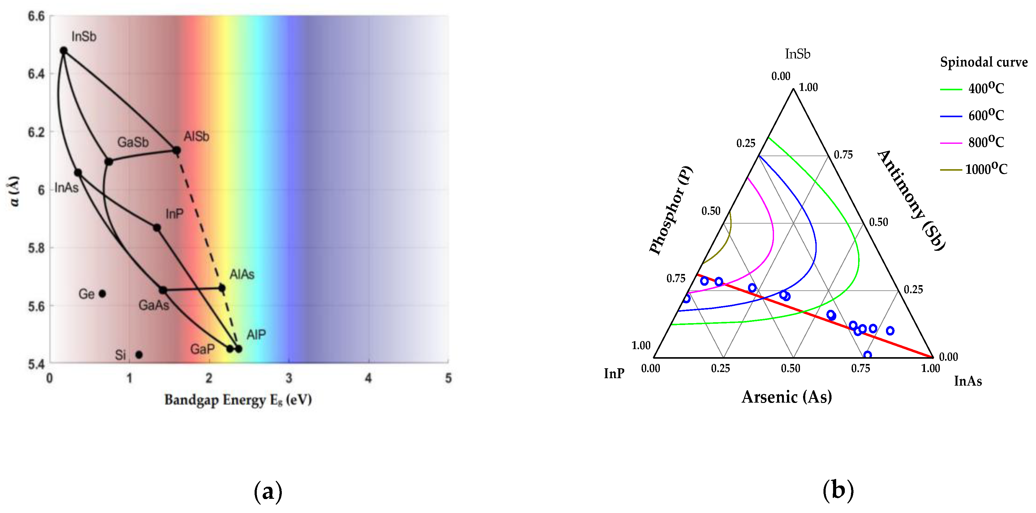
Figure 2.
Comparative study of our rigid-ion model calculations of the phonon dispersions (left panel) and one phonon density of states (right panel) for the zinc-blende indium pnictides: (a) InP, (b) InAs and (c) InSb materials. Full colored lines indicate RIM results [57] while different colored symbols represent data either from INS and/or Raman scattering spectroscopy [53,54,55,56].
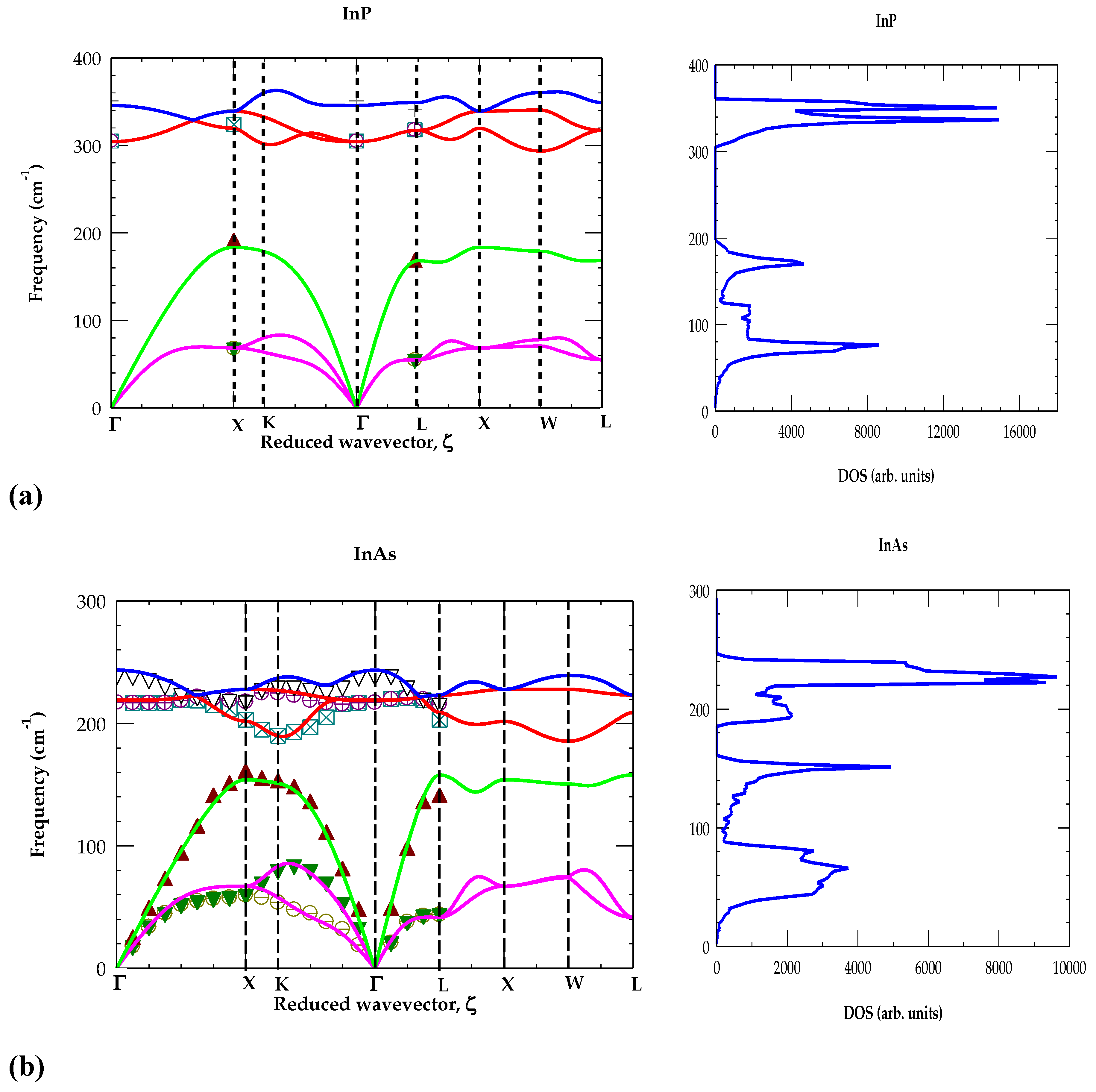
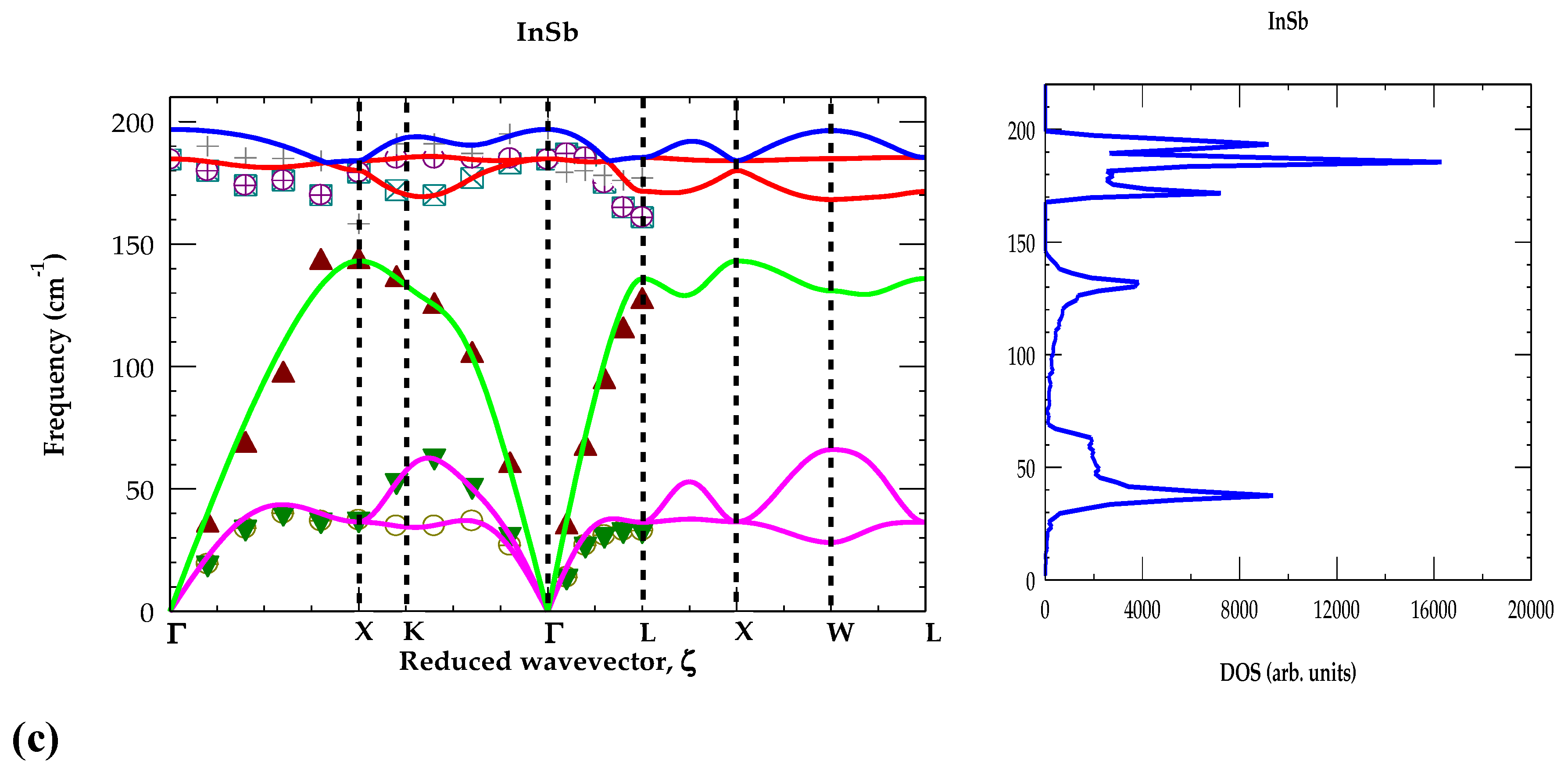
Figure 3.
Room temperature Raman spectra of eight different GS-MBE grown InAs1-x-ySbxPy/n-InAs samples with increasing As. Different colored curved lines are added as a guide to the eye showing major trends of vibrational peaks of three binary In-P, In-As and In-Sb components (see text).
Figure 3.
Room temperature Raman spectra of eight different GS-MBE grown InAs1-x-ySbxPy/n-InAs samples with increasing As. Different colored curved lines are added as a guide to the eye showing major trends of vibrational peaks of three binary In-P, In-As and In-Sb components (see text).
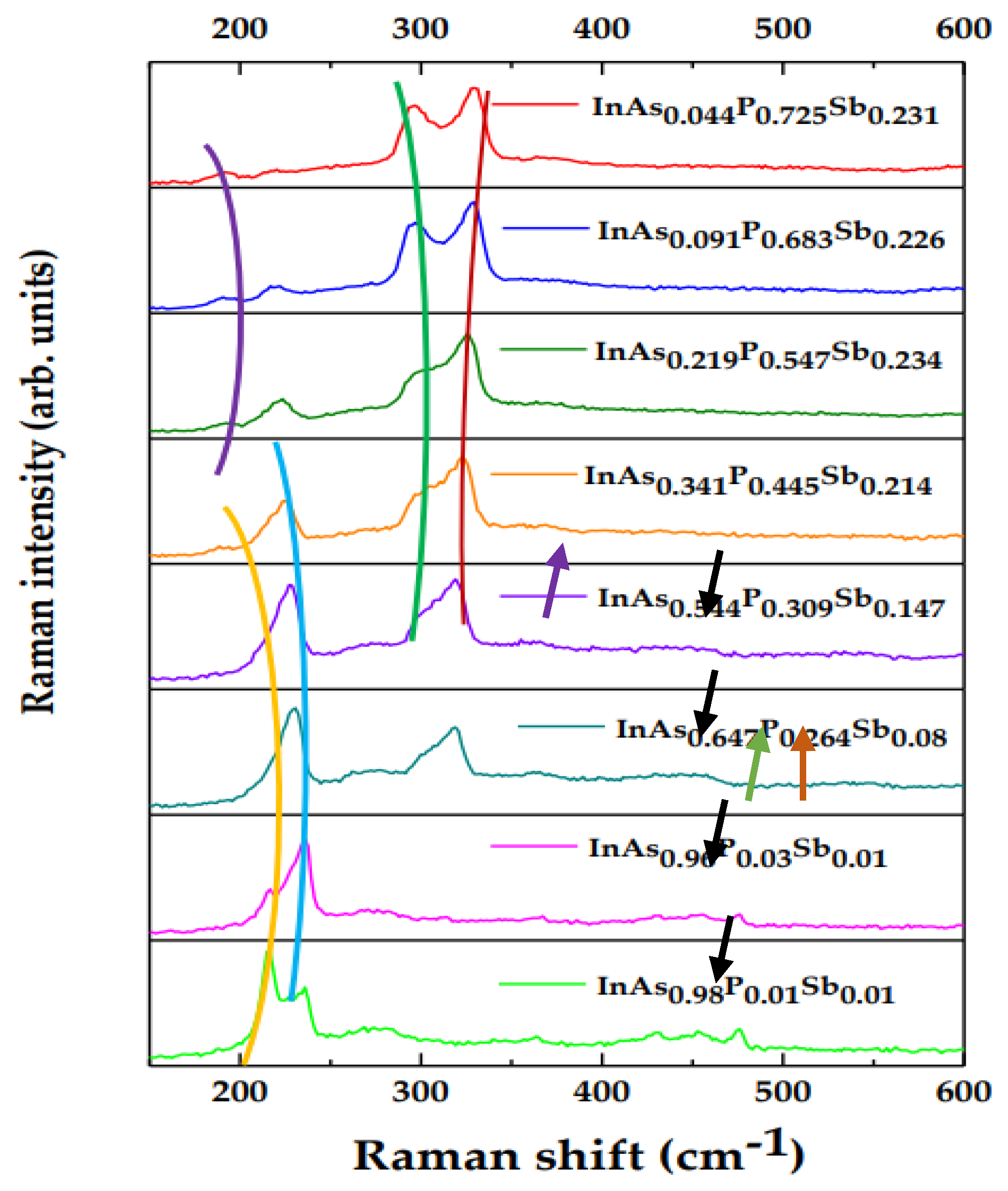
Figure 4.
Comparison of experimental FTIR spectroscopic data (blue colored lines) (a-c) of different compositions with a reasonably good theoretical fit obtained by using a transfer matrix method (red colored open square) for InAs1-x-ySbxPy/n-InAs epilayers (see text).
Figure 4.
Comparison of experimental FTIR spectroscopic data (blue colored lines) (a-c) of different compositions with a reasonably good theoretical fit obtained by using a transfer matrix method (red colored open square) for InAs1-x-ySbxPy/n-InAs epilayers (see text).
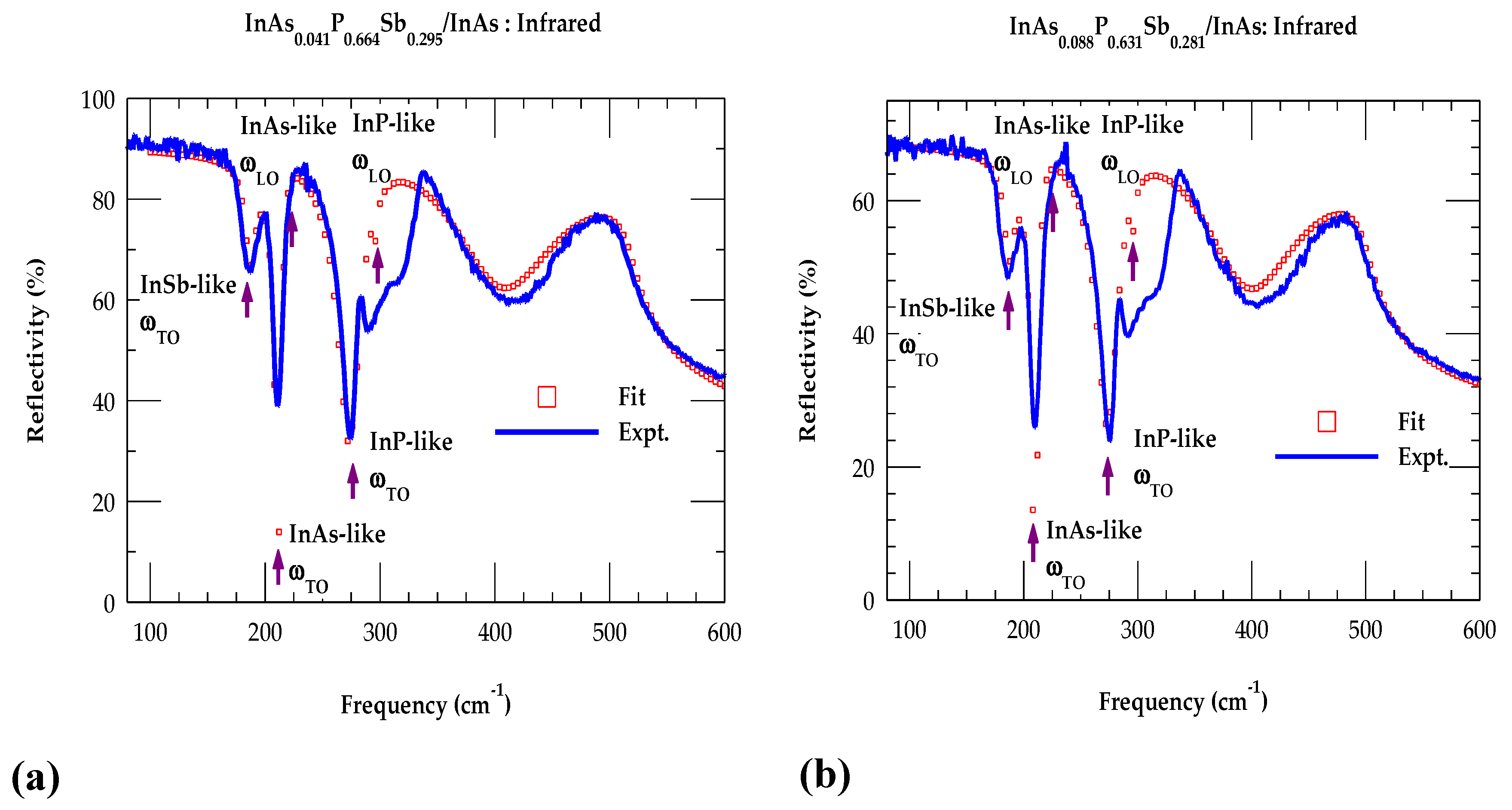
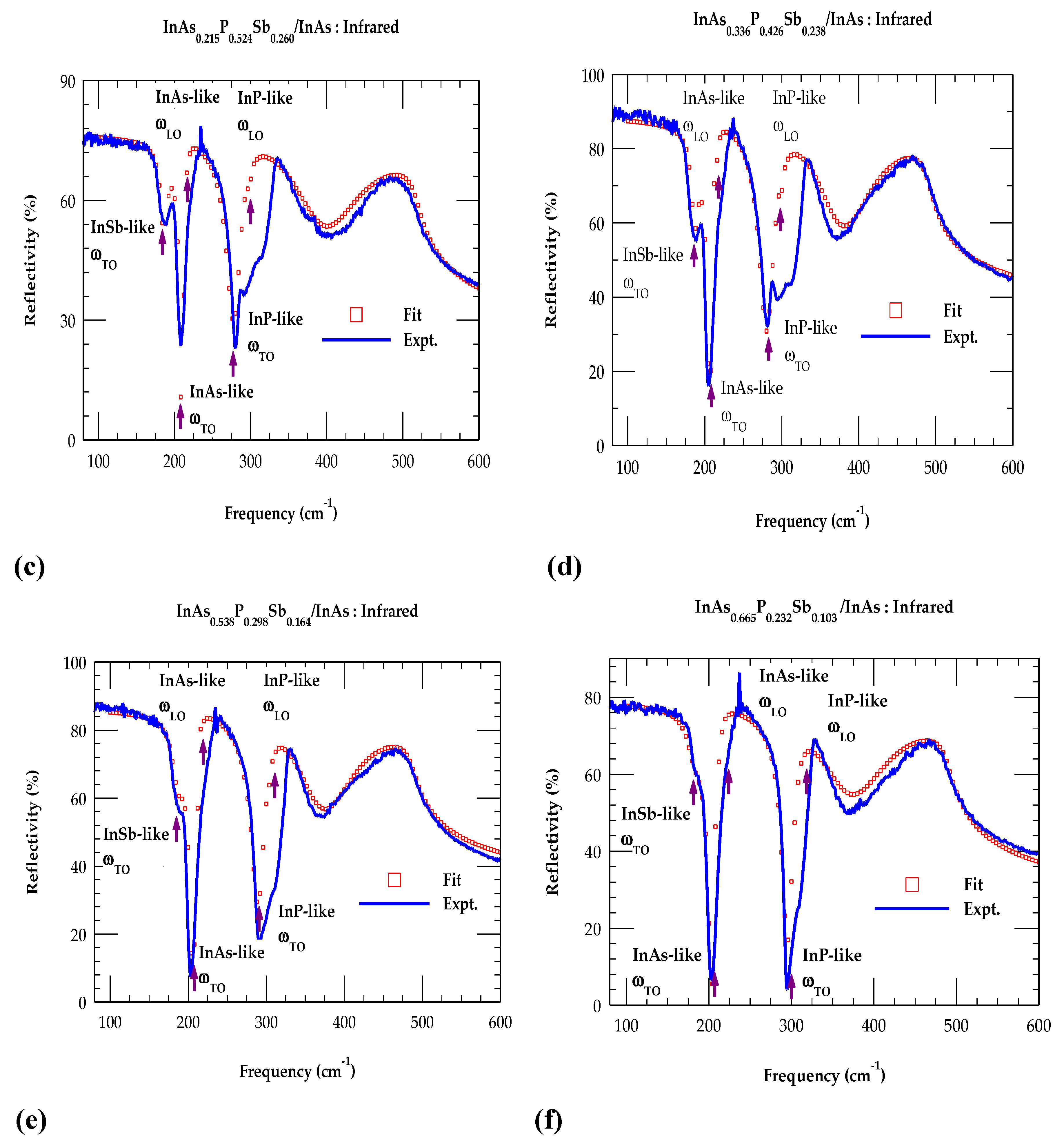
Figure 5.
Composition dependent three-phonon mode behavior in InAs1-x-ySbxPy quaternary alloys. Red solid triangles and blue solid inverted triangles represent the experimental data. observed by Raman scattering and FTIR spectroscopy (cf. Section 3.3 and 3.4).
Figure 5.
Composition dependent three-phonon mode behavior in InAs1-x-ySbxPy quaternary alloys. Red solid triangles and blue solid inverted triangles represent the experimental data. observed by Raman scattering and FTIR spectroscopy (cf. Section 3.3 and 3.4).
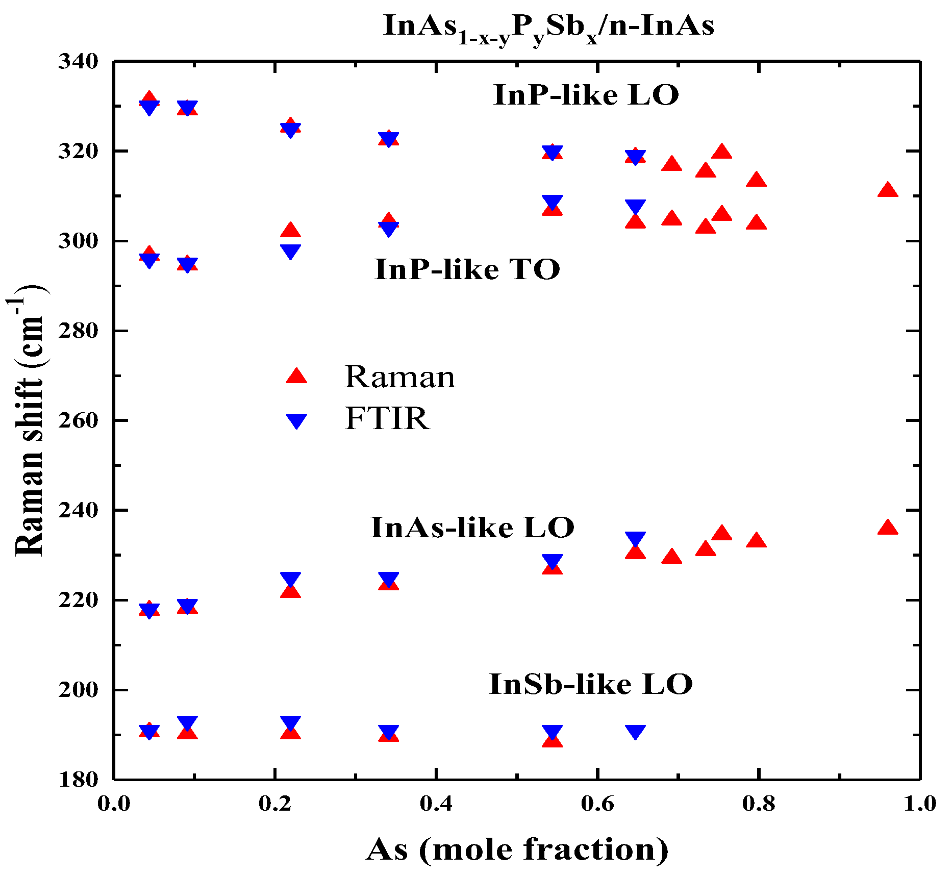
Figure 6.
(a) Fourier transformed EXAFS c(R) P K-edge spectra versus R for InAs1-x-ySbxPy/GaAs samples of different compositions x, y, (b) same key as 6 (a) but for c(R) In K-edge spectra versus R.
Figure 6.
(a) Fourier transformed EXAFS c(R) P K-edge spectra versus R for InAs1-x-ySbxPy/GaAs samples of different compositions x, y, (b) same key as 6 (a) but for c(R) In K-edge spectra versus R.
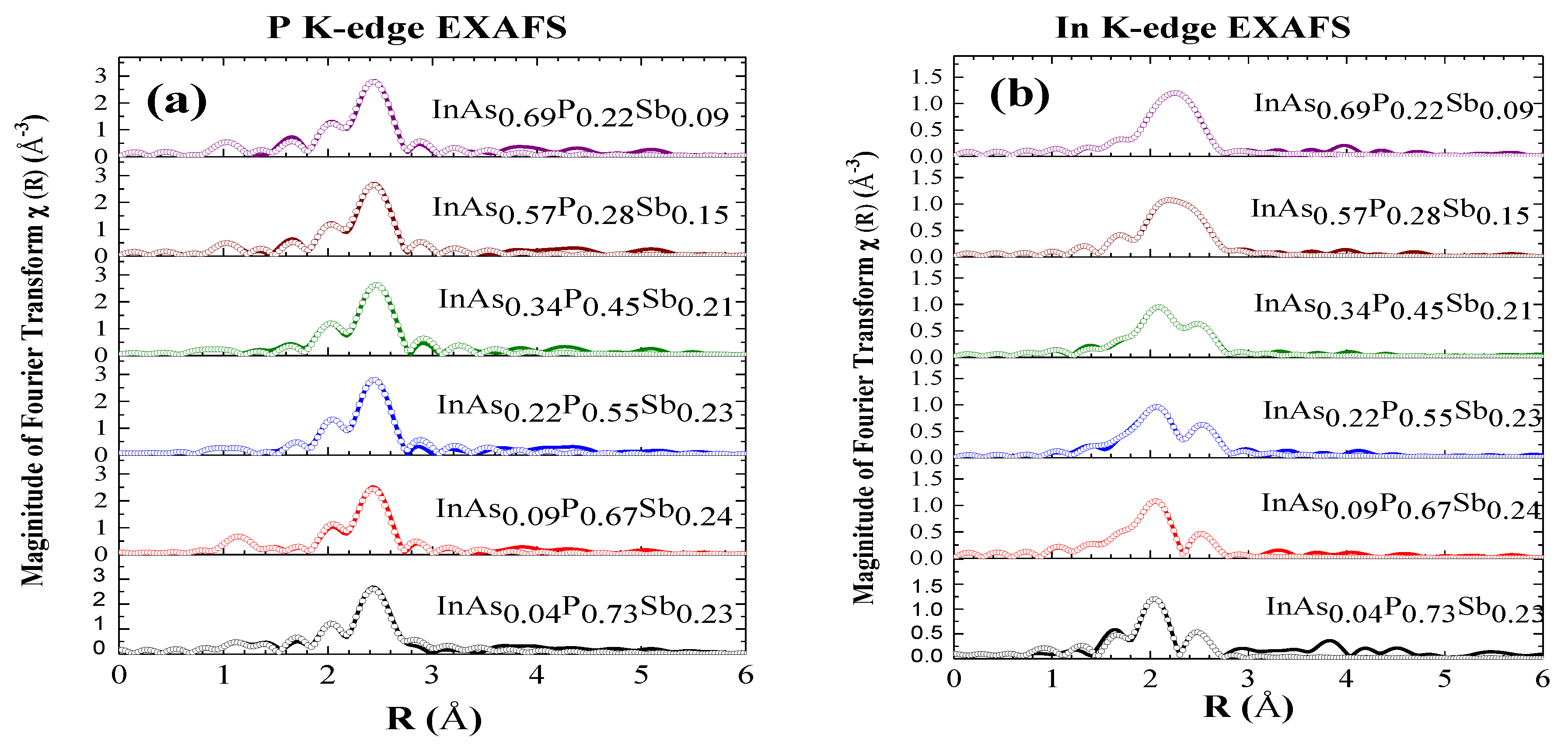
Figure 7.
(a) Fourier transformed EXAFS c(R) P K-edge spectra versus R for InAs1-x-ySbxPy samples of different compositions x, y, before double crystal monochromator energy calibration, Experimental results are indicated by using different color symbols, while the solid lines of different color represent the fitted data. (b) same key as 7 (a) but for c(R) In K-edge spectra versus R, after double crystal monochromator energy calibration.
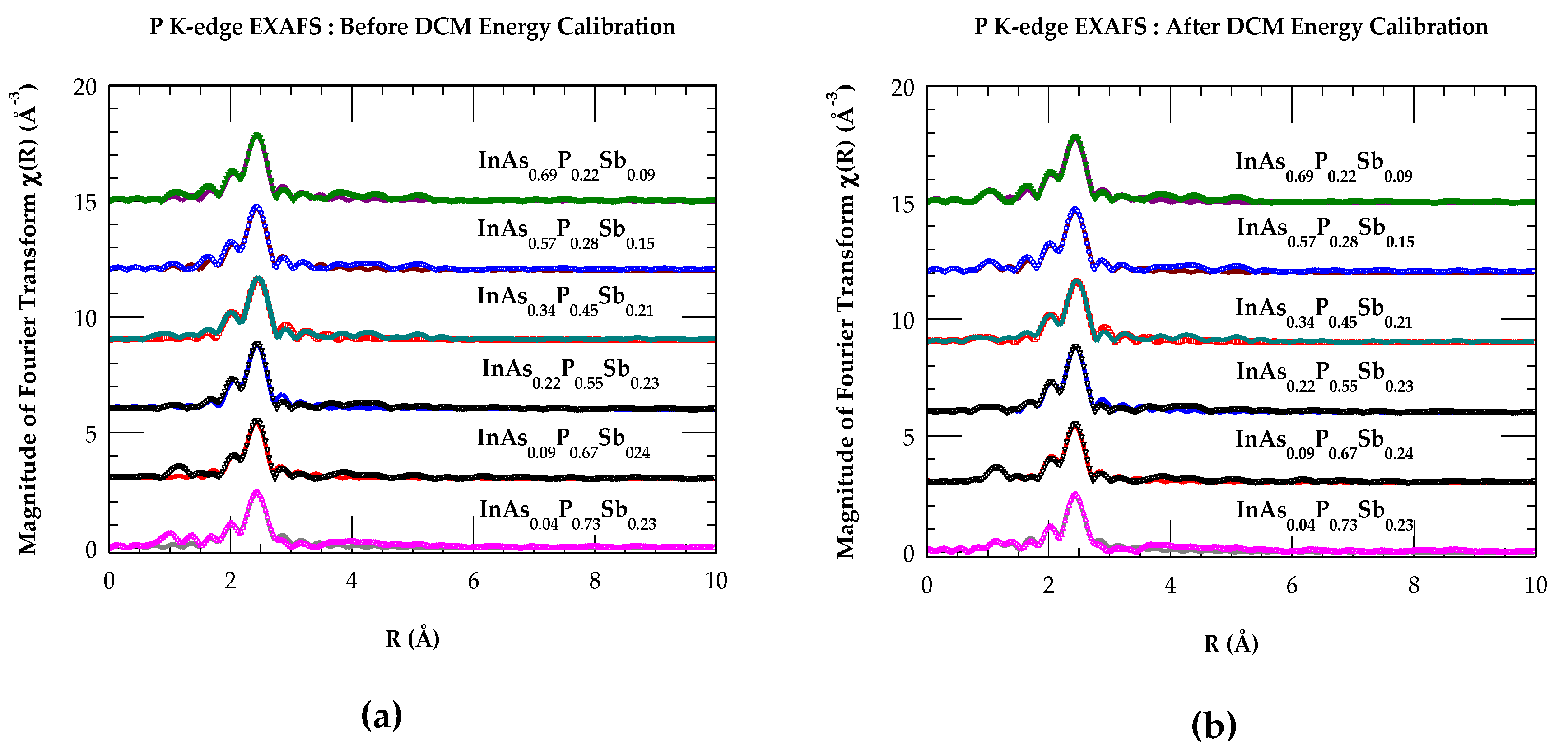
Figure 8.
Bond lengths variation as a function of As fraction for InAs1-x-ySbxPy/GaAs epilayers. The results represent careful analysis of the EXAFS data and by using a VFF model (see text).
Figure 8.
Bond lengths variation as a function of As fraction for InAs1-x-ySbxPy/GaAs epilayers. The results represent careful analysis of the EXAFS data and by using a VFF model (see text).
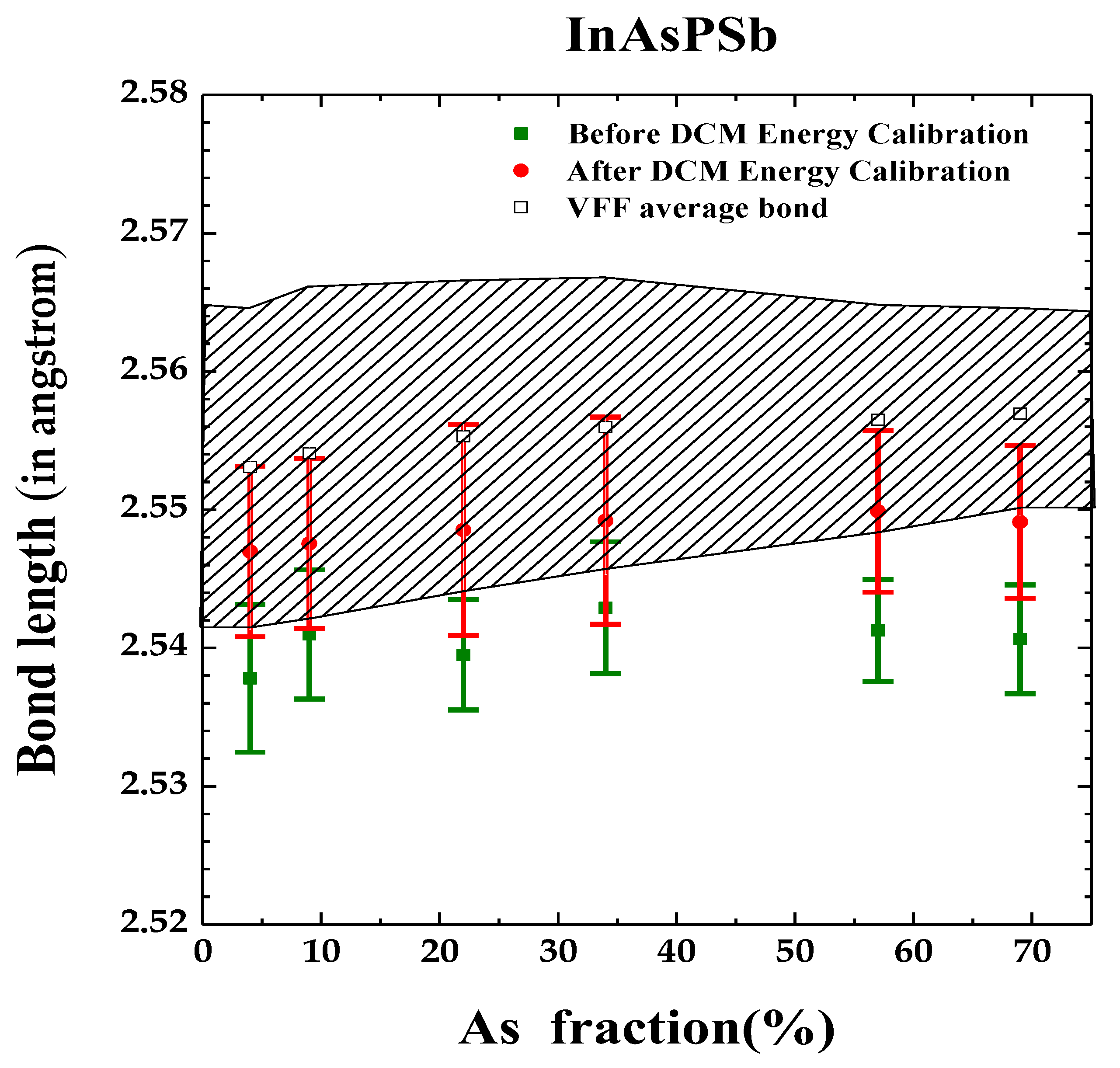
Figure 9.
(a) For InAs1-x-yPySbx/GaAs samples, different color curves represent the relationship between the distortion energy (cal./mole) and the ratio az/axy. Calculations are performed using a VFF model with supercells having different alloy compositions. The points with different color symbols on the curves correspond to the distortion energy values calculated by substituting lattice constants measured via the reciprocal space mapping (RSM). The distortion energy decreases as the As composition increases. (b) Each point in this plot denotes additional distortion energy generated when an InAs1-x-yPySbx sample deforms from the regular cubic to a structure measured by RSM. The curve represents strain energy calculated using a traditional method with experimental points lying on the strain energy curve (see text).
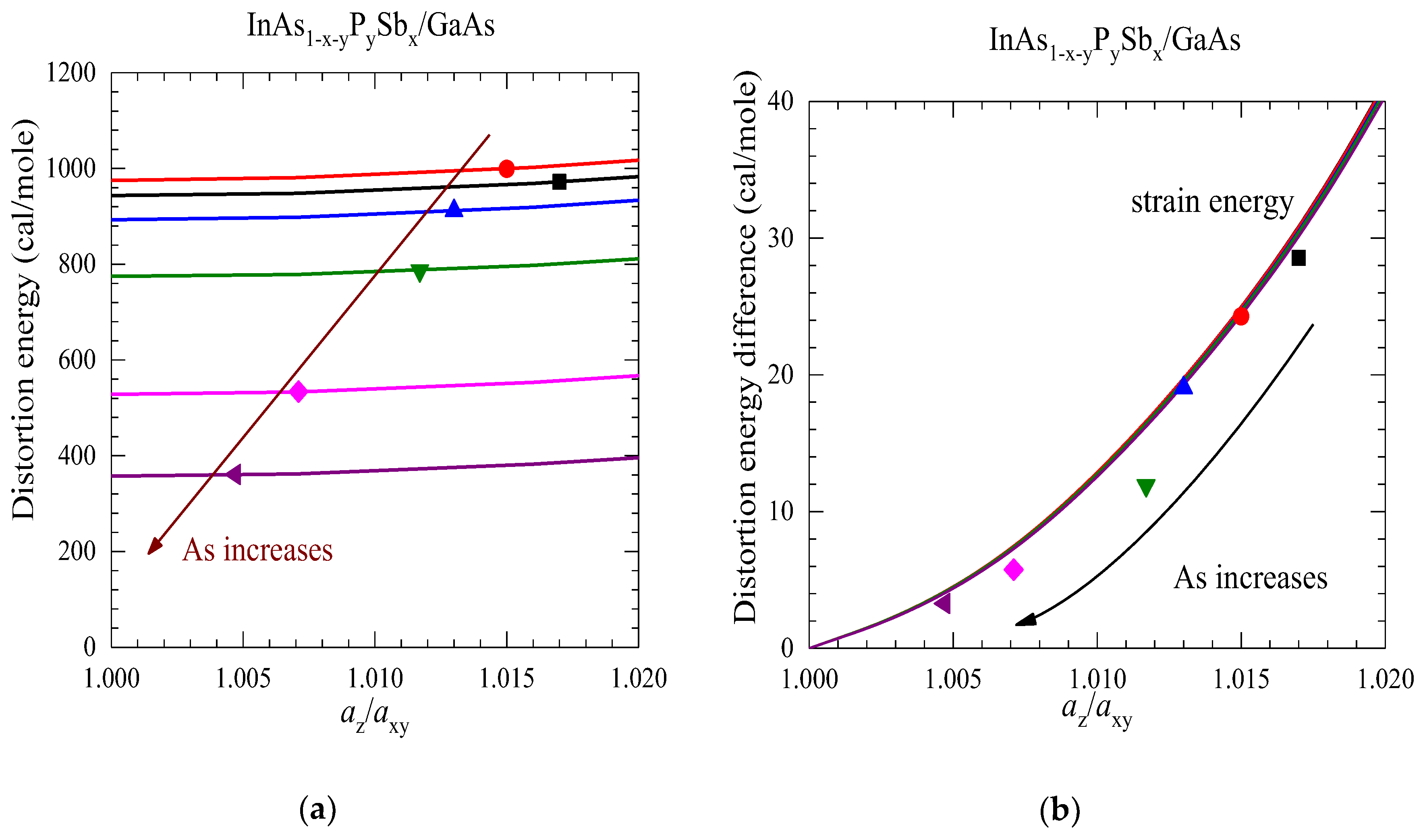

Table 1.
GS-MBE grown high quality InAs1-x-ySbxPy ∼1µm thick samples on n-InAs and GaAs using VG V80H reactor [41] by setting the substrate temperature between ~ 470 oC -480 oC. Compositions of As, P and Sb were determined by a JEOL JXA-8200 electron probe micro-analyzer [41] (see text).
| InAs1-x-ySbxPy samples |
AsH3 (Torr) | PH3 (Torr) |
In/Sb (BEP) | As | Sb | P |
|---|---|---|---|---|---|---|
| S1 S2 S3 S4 S5 S6 S7 S8 S9 S10 S11 S12 S13 S14 S15 S16 |
700 700 700 700 500 300 200 100 50 0 50 100 200 300 500 700 |
990 500 990 990 990 990 990 990 990 900 990 990 990 990 990 990 |
1.98 1.98 2.03 2.03 2.03 2.03 1.89 1.89 1.89 1.60 1.89 1.89 1.89 2.03 2.03 2.03 |
0.795 0.730 0.647 0.690 0.570 0.340 0.220 0.090 0.040 0.000 0.041 0.088 0.215 0.336 0.538 0.665 |
0.101 0.109 0.089 0.090 0.150 0.210 0.230 0.240 0.230 0.480 0.295 0.281 0.260 0.238 0.164 0.103 |
0.104 0.161 0.264 0.220 0.280 0.450 0.550 0.670 0.730 0.520 0.664 0.631 0.524 0.426 0.298 0.232 |
Table 2.
Rigid-ion-model (RIM) [57] calculation of optical phonon frequencies (in cm-1) of binary InP, InAs and InSb are compared with others. Atomic masses (amu) of group V atoms are also given.
Table 2.
Rigid-ion-model (RIM) [57] calculation of optical phonon frequencies (in cm-1) of binary InP, InAs and InSb are compared with others. Atomic masses (amu) of group V atoms are also given.
| Oura) | Others b) | ||||
| Binary Compound |
(cm-1) |
(cm-1) |
(cm-1) |
(cm-1) |
Atomic mass of group V atom |
| InP | 346 | 304 | 343.6-345.2 | 304.5-306.0 | 30.97 |
| InAs | 243 | 219 | 238.8 - 244.0 | 217.3-219.0 | 74.92 |
| InSb | 196 | 185 | 190.8-197.0 | 179.9-185.0 | 121.76 |
Table 3.
Summary of the EXAFS fitting results of vertical az, horizontal lattice constant axy and their az/axy ratio for different InAs1-x-yPySbx/GaAs GS-MBE grown epilayers.
Table 3.
Summary of the EXAFS fitting results of vertical az, horizontal lattice constant axy and their az/axy ratio for different InAs1-x-yPySbx/GaAs GS-MBE grown epilayers.
| InAs1-x-yPySbx | ||||||
|---|---|---|---|---|---|---|
| Sample # | As | P | Sb | az (Å) | axy (Å) | az /axy |
| S9 | 0.04 | 0.73 | 0.23 | 6.0633 | 5.9621 | 1.017 |
| S8 | 0.09 | 0.67 | 0.24 | 6.0705 | 5.9800 | 1.015 |
| S7 | 0.22 | 0.55 | 0.23 | 6.0916 | 6.0113 | 1.013 |
| S6 | 0.34 | 0.45 | 0.21 | 6.0941 | 6.0243 | 1.012 |
| S5 | 0.57 | 0.28 | 0.15 | 6.0818 | 6.0387 | 1.007 |
| S4 | 0.69 | 0.22 | 0.09 | 6.0623 | 6.0333 | 1.005 |
Table 4.
Summary of structural parameters (cf. Section 4.5) by fitting EXAFS results for different GS-MBE grown InAs1-x-yPySbx/GaAs samples before and after DCM energy calibration.
Table 4.
Summary of structural parameters (cf. Section 4.5) by fitting EXAFS results for different GS-MBE grown InAs1-x-yPySbx/GaAs samples before and after DCM energy calibration.
| InAs1-x-yPySbx | ||||||||||
|---|---|---|---|---|---|---|---|---|---|---|
| Sample # | a) | b) | ) a) | ) b) | N a) | N b) | R (Å) a) | R (Å) b) | ΔR a) | ΔR b) |
| S9 | 0.720 | 0.768 | 0.00356 | 0.00416 | 3.57723 | 4.11917 | 2.53780 | 2.54698 | 0.03454 | 0.01794 |
| S8 | 0.580 | 0.559 | 0.00253 | 0.00221 | 2.97051 | 3.15081 | 2.54098 | 2.54755 | 0.03620 | 0.01476 |
| S7 | 0.693 | 0.685 | 0.00261 | 0.00238 | 3.45424 | 4.46523 | 2.53950 | 2.54852 | 0.02482 | 0.00611 |
| S6 | 0.716 | 0.699 | 0.00257 | 0.00247 | 3.86432 | 4.22846 | 2.54290 | 2.54920 | 0.01483 | 0.01184 |
| S5 | 0.690 | 0.691 | 0.00261 | 0.00252 | 3.86611 | 4.79094 | 2.54127 | 2.54988 | 0.02560 | 0.01204 |
| S4 | 0.724 | 0.728 | 0.00259 | 0.00251 | 3.63522 | 4.636544 | 2.54062 | 2.54911 | 0.02218 | 0.01173 |
a) Before DCM energy calibration b) After DCM energy calibration
Disclaimer/Publisher’s Note: The statements, opinions and data contained in all publications are solely those of the individual author(s) and contributor(s) and not of MDPI and/or the editor(s). MDPI and/or the editor(s) disclaim responsibility for any injury to people or property resulting from any ideas, methods, instructions or products referred to in the content. |
© 2025 by the authors. Licensee MDPI, Basel, Switzerland. This article is an open access article distributed under the terms and conditions of the Creative Commons Attribution (CC BY) license (http://creativecommons.org/licenses/by/4.0/).
Copyright: This open access article is published under a Creative Commons CC BY 4.0 license, which permit the free download, distribution, and reuse, provided that the author and preprint are cited in any reuse.


