Submitted:
09 October 2025
Posted:
09 October 2025
You are already at the latest version
Abstract
We developed a 2.2um Backside Illuminated (BSI) Global Shutter (GS) pixel with true charge-domain Correlated Dou-ble Sampling (CDS). A thick-film epitaxial deep DTI (Deep Trench Isolation) process was implemented to enhance 1/PLS (Parasitic Light Sensitivity) using a dual depth DTI structure. The thickness of the epitaxial substrate was 8.5 um. This structure was designed using optical simulation. By using a thick epitaxial substrate, it is possible to reduce the amount of light that reaches the memory node. Dual-depth DTI, which shallows the DTI depth on the readout side, makes it possible to read signals from the PD to the memory node smoothly. To achieve this structure, we developed a process for thick epitaxial substrate, and the dual-depth DTI can be fabricated with a single mask. This newly developed pixel rep-resents the smallest ever charge-domain GS pixel to date. Despite its compact size, this pixel achieved high QE (83%) and 1/PLS of over 10,000. The pixel maintains 80% of its peak QE at ±15 degrees. 1/PLS is stable even when the F# is small.
Keywords:
CMOS image sensor
; global shutter
; charge domain
; parasitic light sensitivity
; dark current
; modulation transfer function
1. Introduction
The demand for small pixel-size Global Shutter (GS) sensors, which can take images without distortion for fast-moving objects continues to grow. This function is highly desirable for machine vision and high-grade movie camera. Previously, we demonstrated a Front-Side Illuminated (FSI) 2.5µm GS pixel using a light pipe structure [1]. However, in FSI, as the pixel size becomes smaller, the proportion of the wiring area increases, and the optical aperture becomes smaller. The BSI structure is suitable for enlarging the optical aperture, achieving high QE, and expanding the degree of freedom in wiring design. Consequently, the development of BSI GS pixels is underway [2]. Another critical requirement for small pixels and low photon counts is noise suppression. Charge-domain pixels are particularly well-suited for reducing pixel noise, making them ideal for visible light sensors [3,4]. However, BSI introduces challenges in suppressing PLS. For a high-performance GS sensor, the target 1/PLS value should be around 10,000 or higher. In addition, PLS needs to be suppressed even when the F# becomes small. Furthermore, even if the pixel size becomes smaller, a wide angular response is required. In this paper, we present a 2.2µm charge-domain BSI GS pixel with best-in-class performance, achieved through an especially deep dual-depth DTI structure and a thick-epi process.
2. Device Structure
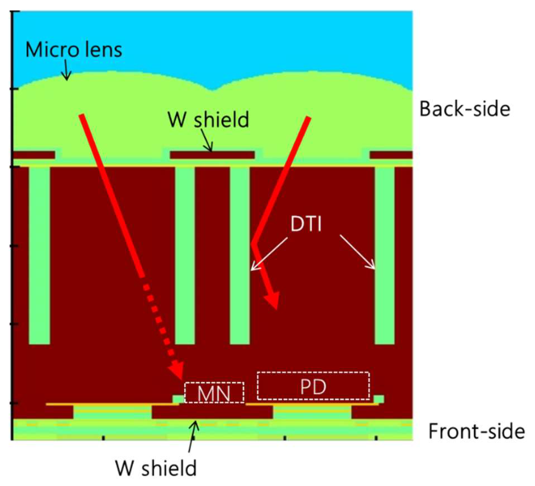
Figure 1 presents a basic cross-section of the charge-domain type BSI GS pixel [5]. Incident light is focused by a micro-lens and directed to the Photo Diode (PD) area, which is surrounded by DTI. A fully buried Memory Node (MN) is positioned near the front-side surface to store charges until readout. This fully buried MN structure is effective in reducing dark current, as previously reported [6].
PLS arises when photoelectrons are generated in the MN or when electrons generated elsewhere in the pixel are collected by the MN. This parasitic signal can introduce image artifacts in GS operation, particularly in highly dynamic scenes. PLS from photoelectrons generated outside the MN can be effectively mitigated through device design that ensures the PD collects all generated photoelectrons. In BSI pixels, Tungsten shield (WS) is implemented on both, the front and back sides [7,8]. The WS on the backside prevents direct incidence of light into the MN. On the other hand, the WS on the front side prevents reflected light from the wiring layer from entering the MN. Light penetration into the MN is further minimized by DTI.
3. Development of 2.2 um BSI Charge Domain Global Shutter Pixel
3.1. Optical and Pixel Design
The optical design will be described below. First, the effect of DTI will be described. Since the DTI is filled with a material with a low refractive index, such as an oxide film, the light inside the Si is totally reflected by the DTI. This significantly reduces the penetration of light into the MN. However, below the bottom of the DTI, the light in the PD is not reflected and light penetrates into the MN. Therefore, deeper DTI is important for suppressing PLS.
Figure 3.
Effects of DTI structure and points for improvement.
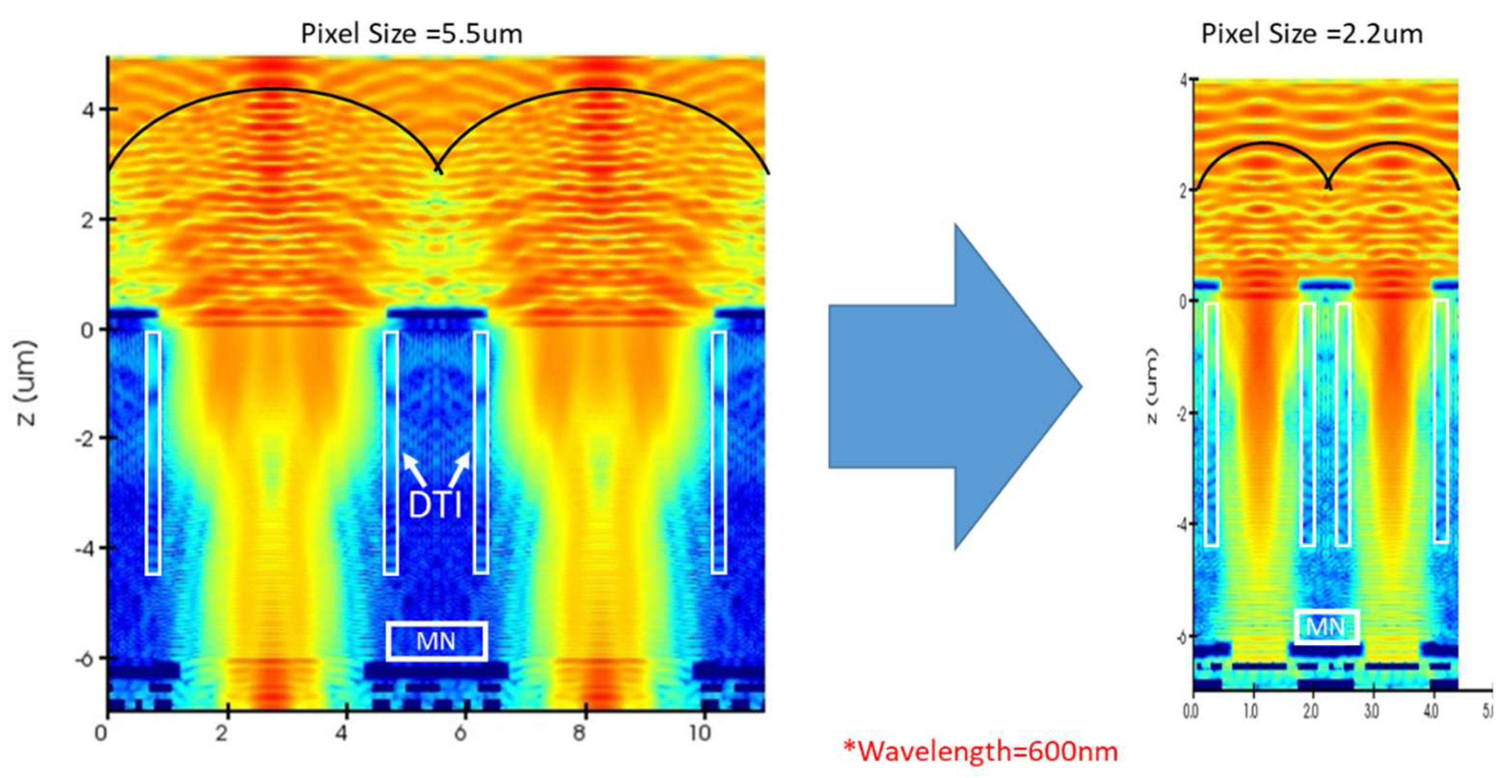
Next, the effect of reducing the pixel size will be described. Figure 4 compares the electric field distribution when the pixel size is 5.5 um and when it is 2.2 um. Both are the results of optical simulations, and the epi thickness was set to 6 um. When the pixel size is 5.5 um, the distance between the focused point and the MN is large, so little light penetrates the MN. On the other hand, when the pixel size is 2.2 um, the distance between the focused light and the MN is close, so the light easily penetrates into the MN. Thus, as the pixel size becomes smaller, it becomes easier for light to penetrate into the MN, so increasing the depth of DTI is effective but not sufficient.
Figure 4.
Impact of pixel size reduction.
Since it was predicted that simply deepening the DTI would not be sufficient to suppress PLS in small pixels, we investigated increasing the thickness of the epitaxial film. Figure 4 shows the relationship between epitaxial film thickness and absorption. When the epitaxial film thickness is 6 um, blue light is completely absorbed by the silicon. Green light is also almost completely absorbed. However, only about 9% of red light is absorbed. As can be seen from Figure 4, the thicker the epitaxial film, the more red light is absorbed, so a thick epitaxial film is desirable. However, there is a limit to how thick the film can be due to the actual manufacturing process. Therefore, we decided to increase the epi thickness in the newly developed BSI GS. By increasing the epi thickness to 8.5 um, only red light reaches the MN, and blue and green light do not reach the MN, resulting in a significant improvement in PLS. The combined use of thick Epi and deep DTI is expected to significantly reduce PLS. However, when forming deep DTI, care must be taken when reading out signals from PDs.
Figure 4.
Relationship between epitaxial film thickness and absorption.
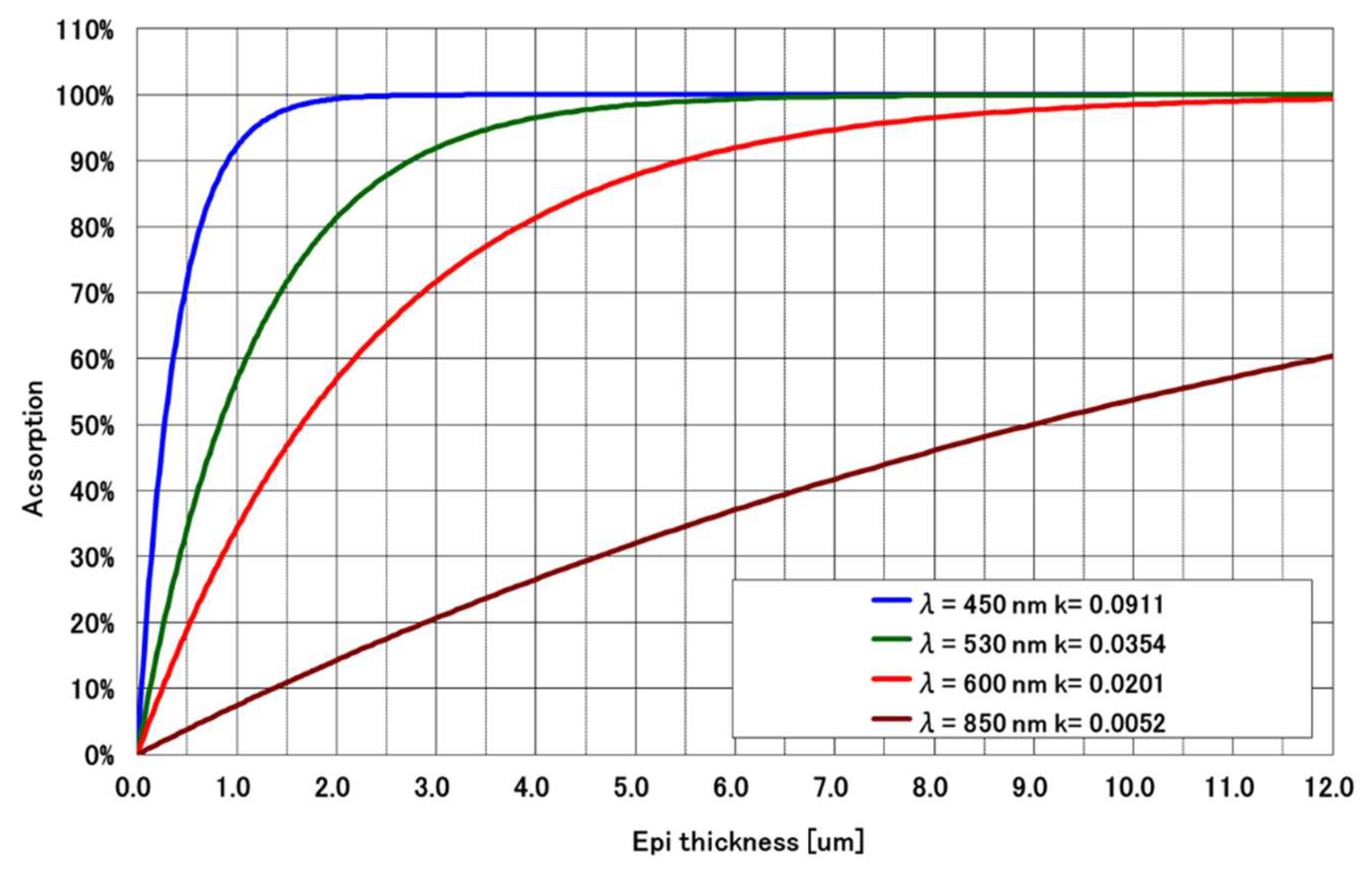
Figure 4 shows the bottom shape of the DTI of the newly developed BSI_GS. The DTI depth is different between the readout side and the non-readout side of the MN. Two primary factors determine the depth of DTI on the readout side. First, a gap of approximately 1.5 um is necessary to enable signal readout from the PD to the MN. Second, it is essential to suppress electron diffusion current within the p-type well from reaching the memory node.
Figure 4.
Dual depth DTI structure.
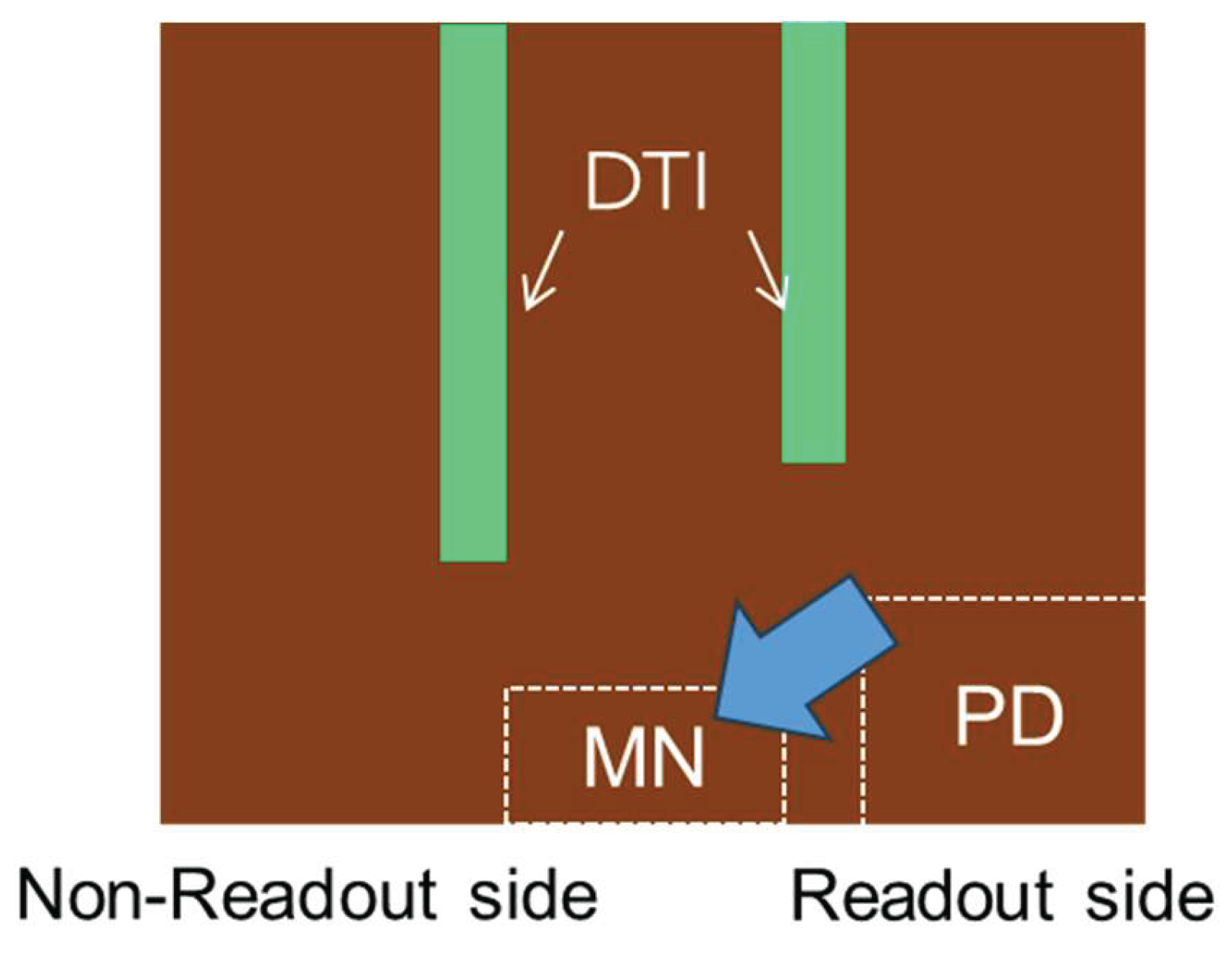
Figure 5 illustrates the expected electron diffusion current flow in the p-type well surrounding the memory node. When a deeper DTI is implemented on the readout side, photo-generated electrons located between the two DTIs are likely to diffuse toward the memory node due to the absence of alternative electron pathway within the p-type well. This diffusion current contributes as an additional source of PLS. In contrast, a shallower DTI on the readout side allows these electrons to be drained into the photodiode, thereby reducing PLS. The DTI on the non-readout side should be as deep as possible to prevent light from penetrating into the MN, so a dual-depth DTI structure was adopted.
Figure 6 shows the results of optical simulations using the 3D-FDTD method, highlighting the effects of a thicker epitaxial layer and deeper DTI. The deep DTI effectively blocks light from reaching the MN, while a thicker epitaxial layer reduces light penetration. A 6µm epitaxial thickness allows green and red light to reach the MN, making PLS reduction difficult. However, with an 8.5µm epitaxial thickness, green light is entirely blocked, and red light intensity is significantly reduced. This ensures low PLS under short-wavelength light sources used in inspection and measurement applications. Next, the optimal DTI depth was determined through TCAD simulations, indicating that an epitaxial thickness of 8.5µm and DTI depths of 7.2µm and 7.5µm would achieve a 1/PLS of over 10,000.
3.2. Process Design
The main process challenges involved fabricating the thick epitaxial layer and the deep dual-depth DTI structure. For the first time, we employed an 8.5µm-thick epitaxial layer in a BSI GS pixel, comparable to the thickest commercial BSI GS products. We newly optimized the wafer thinning process down to 8.5um epitaxial layer which was made of the new starting material. In accordance with the thick-epi-process, alignment mark was also optimized to meet the requirement of process feasibility and alignment accuracy for both of front-side and back-side as shown in Figure 7. Mark fabrication process has evolved from that of the conventional BSI. The dedicated mark process comprises of the deep etching and deep-trench filling. The dual-depth DTI structure (7.2µm and 7.5µm) was achieved with a cost-effective, single-mask process. The DTI layout, including its length and width, were carefully optimized and the actual DTI depth was successfully realized to meet the desirable depth above by using single etching process.
Although DTI sidewalls are a known sources of photodiode dark current, which is typically proportional to DTI depth, we successfully suppressed dark current by optimizing the DTI formation process, which includes DTI etching condition, surface treatment process and the film formation process for passivation and filling within the DTI.
4. Results
Figure 8 presents the cross-section of the newly developed BSI GS sensor, fabricated using a 65nm stacked BSI process with three Cu layers on the sensor wafer. The superior performance of the dual-depth DTI and thick epitaxial substrate was confirmed.
Figure 9 shows QE curves for both color and monochrome samples. The QE for the green pixel (530nm) reached 73%, while the QE for blue (450nm) and red (600nm) pixels were 66% and 68%, respectively. The peak QE of the monochrome sample was 83% at 550nm. Despite the small pixel size, a high QE was achieved.
Figure 10 presents the wavelength dependence of 1/PLS, demonstrating values exceeding 10,000 for wavelengths of 570nm or less. This means that devices that use blue or green as a light source do not need to worry about PLS.
Figure 11 illustrates the F# dependence of 1/PLS, showing that the monochrome sample achieved 1/PLS of 10,380 (-80.3dB) at F#=9, while a sample with a 6µm epitaxial thickness had a lower 1/PLS of 4,300. These values are very close to the results of optical simulations. The thick epitaxial and dual-depth DTI structures suppress the deterioration of PLS even when the F# is smaller.
Figure 12 shows the angular response of QE. Despite the small pixel size, QE remains above 80% of the peak value within a range of ±15 degrees.
Figure 13 compares dark current levels between a 6µm epi process and the new deeper-epi, deeper-DTI process. By optimizing DTI etching and buried material, dark current was minimized despite increased DTI depth.
Table 1 summarizes the pixel performance, highlighting a noise level of 0.6e- due to the charge-domain GS-CDS architecture. The pixel array MTF is at least 40% at Nyquist frequency, making this a best-in-class high-resolution, low-noise global shutter sensor.
5. Conclusions
We developed the world’s smallest charge-domain 2.2µm BSI GS pixel, suitable for high-resolution machine vision sensors and consumer applications. To mitigate 1/PLS degradation from pixel miniaturization, we implemented a thicker epitaxial layer and a dual-depth DTI structure. A novel thick-film epi process was developed, achieving a peak QE of 83% (monochrome). The pixel maintains 80% of its peak QE at ±15 degrees.
The 1/PLS achieved 10,380 at F#9, meeting the target of over 10,000. Even at F#2.8, 1/PLS remained high at 9,770 (79.8dB). This innovative design successfully enhances GS sensor performance, offering industry-leading noise suppression and light sensitivity.
Author Contributions
Conceptualization, T.Y. and M.T.; pixel layout and design, M.T.; optical design, T.Y. and Y.N.; chip design, F.A.; process design, Y.N. and M.T.; evaluation, M.T., Y.N. and D.V.; writing—original draft preparation, T.Y., and M.O.; writing—review and editing, M.O., M.T., and T.Y.; supervision, F.A.; project administration, M.O.
Conflicts of Interest
The authors declare no conflict of interest.
References
- T.Yokoyama, et al., High Performance 2.5um Global Shutter Pixel with New Designed Light-Pipe Structure. In Proceeding of the IEDM 2018, San Francisco, USA, 2018.
- Y. Kumagai, et al., Back-Illuminated 2.74um-Pixel-Pitch Global Shutter CMOS Image Sensor with Charge-Domain Memory Achieving 10k e-saturation Signal. In Proceeding of the IEDM 2018, San Francisco, USA, 2018.
- Wang, X.; Bogaerts, J.; Vanhorebeek, G.; Ruythoren, K.; Ceulemans, B.; Lepage, G.; Willems, P.; Meynants, G. A 2.2M CMOS Image Sensor for High Speed Machine Vision Applications. In Proceedings of the IS&T/SPIE Electronic Imaging, San Jose, CA, USA, 26 January 2010; Volume 7536. [Google Scholar]
- Meynants, G. Global shutter pixels with correlated double sampling for CMOS image sensors. Adv. Opt. Technol. 2013, 2, 177–187. [Google Scholar] [CrossRef]
- Lauxtermann, S.; Lee, A.; Stevens, J.; Joshi, A. Comparison of Global Shutter Pixels for CMOS Image Sensors. In Proceedings of the 2007 International Image Sensor Workshop, Ogunquit, ME, USA, 7–10 June 2007. [Google Scholar]
- M. Tsutsui, et al., Development of Low Noise Memory Node in a 2.8um Global Shutter Pixel with Dual Transfer. In Proceedings of the 2017 International Image Sensor Workshop, Hiroshima, Japan, 2017; pp.28.
- Yokoyama, T.; Tsutsui, M.; Nishi, Y.; Mizuno, I.; Dmitry, V.; Lahav, A. High Performance 2.5 um Global Shutter Pixel with New Designed Light-Pipe Structure. In Proceedings of the 2018 International Electron Devices Meeting, San Francisco, CA, USA, 1–5 December 2018. [Google Scholar]
- Velichko, S.; Hynecek, J.J.; Johnson, R.S.; Lenchenkov, V.; Komori, H.; Lee, H.W.; Chen, F.Y. CMOS Global Shutter Charge Storage Pixels with Improved Performance. IEEE Trans. Electron Devices 2015, 63, 106–112. [Google Scholar] [CrossRef]
- Mabuchi, K.; Nakamura, N.; Funatsu, E.; Abe, T.; Umeda, T.; Hoshino, T.; Suzuki, R.; Sumi, H. CMOS Image Sensor Using a Floating Diffusion Driving Buried Photodiode. In Proceedings of the 2004 International Solid-State Circuits Conference, San Francisco, CA, USA, 15–19 February 2004. [Google Scholar]
- K.Ito et al., A Back Illuminated 10um SPAD Pixel Array Comprising Full Trench Isolation and Cu-Cu Bonding with Over 14% PDE at 940nm In Proceeding of the IEDM 2020, Virtual Session, 2020.
Figure 1.
Cross section BSI_GS sensor.
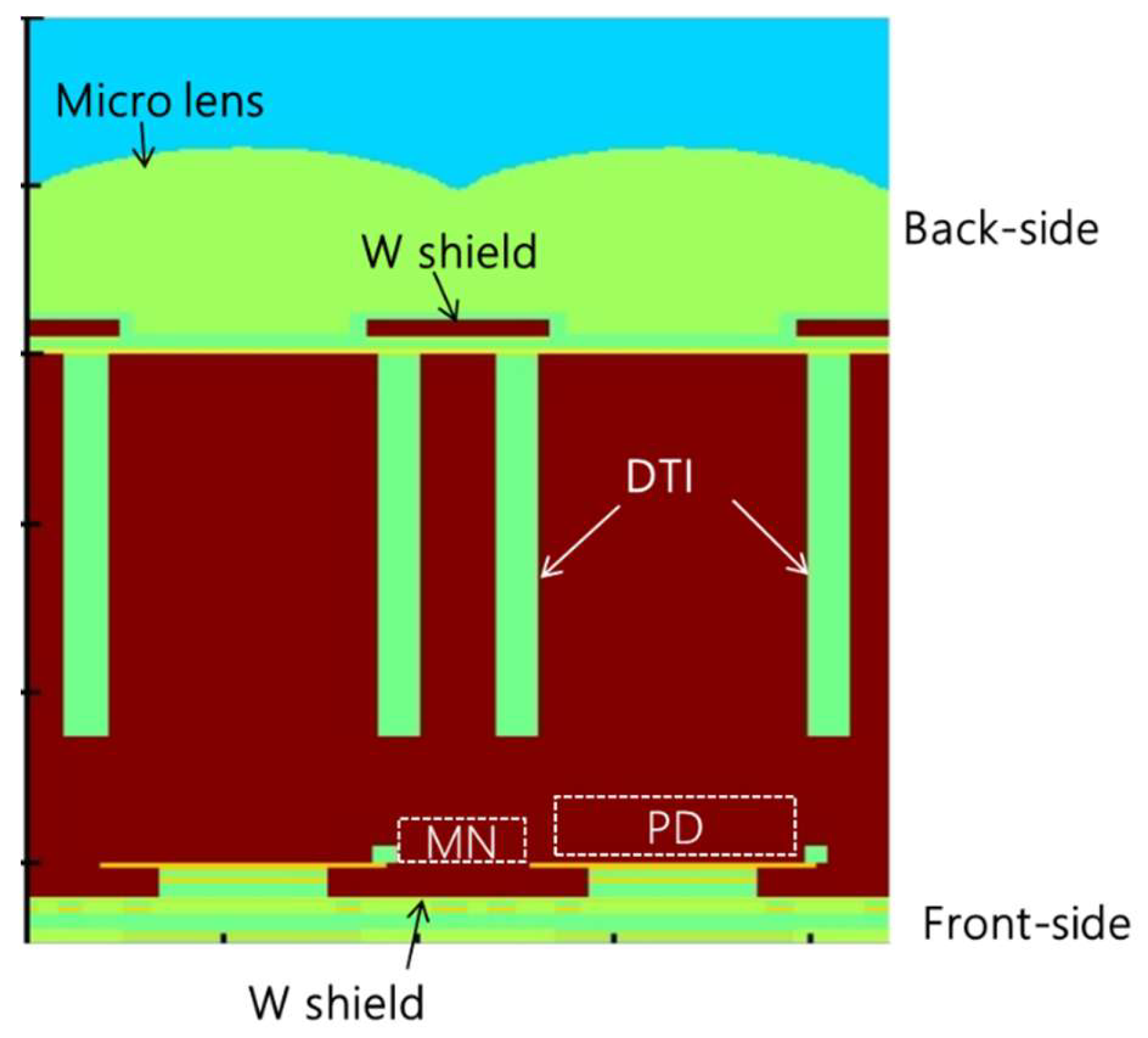
Figure 2.
Pixel circuit schematic of GS pixel.
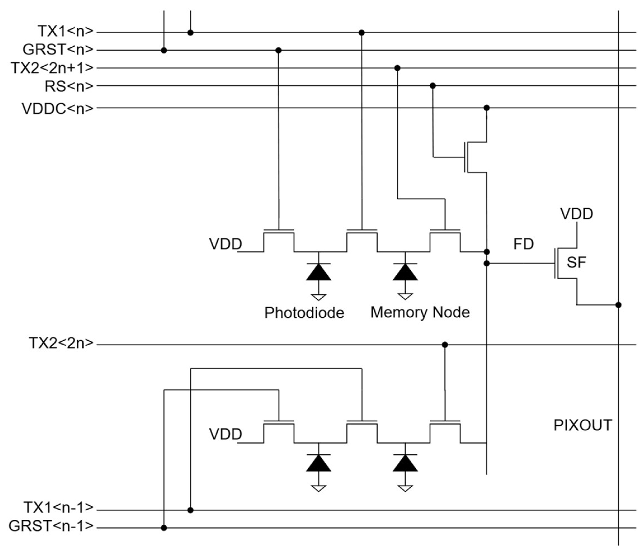
Figure 5.
Schematics illustrating diffusion current flow of electron in the p-type well surrounding the memory node, comparing (a) deeper DTI and (b) shallower DTI configurations on the readout side.
Figure 5.
Schematics illustrating diffusion current flow of electron in the p-type well surrounding the memory node, comparing (a) deeper DTI and (b) shallower DTI configurations on the readout side.
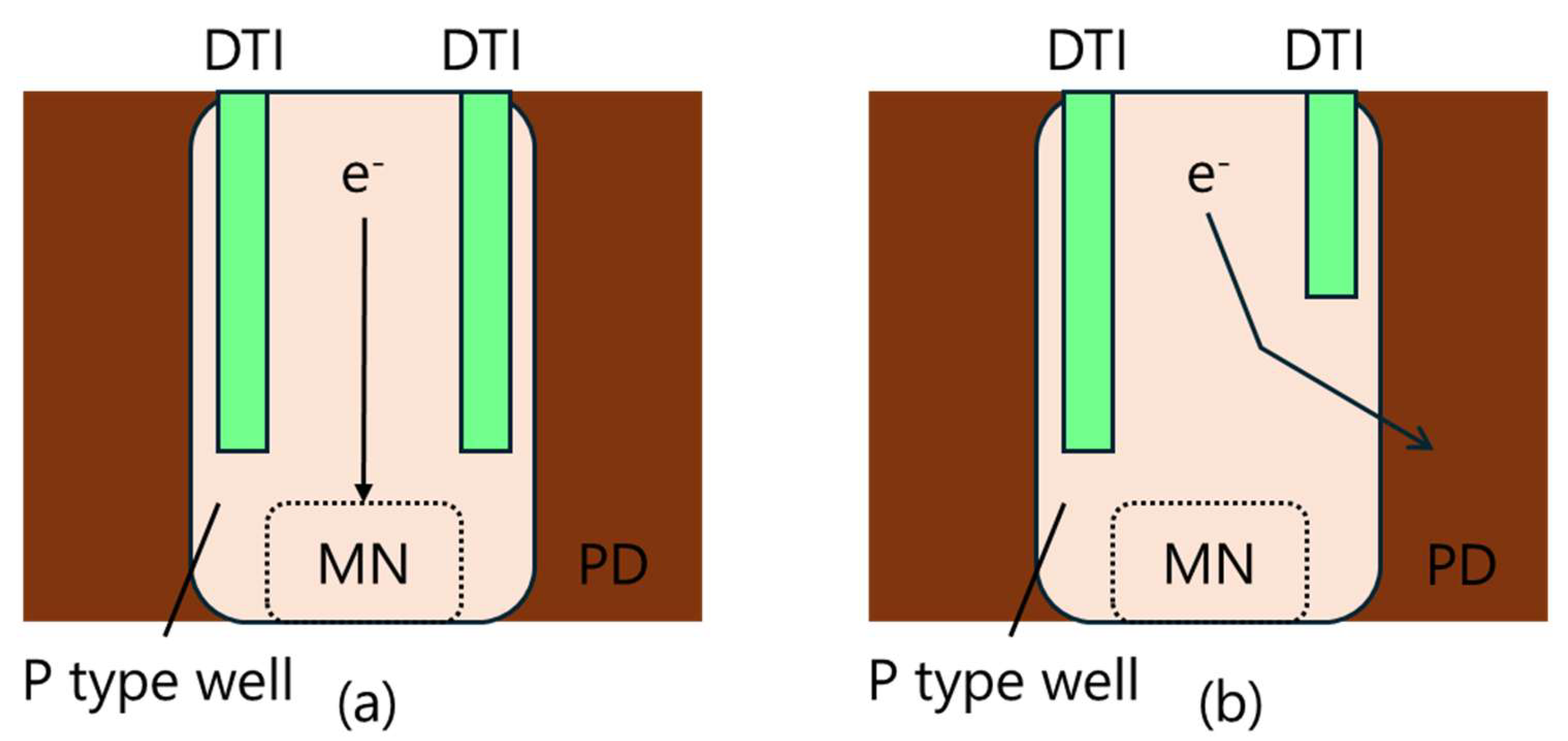
Figure 6.
Simulation results and developed structure.
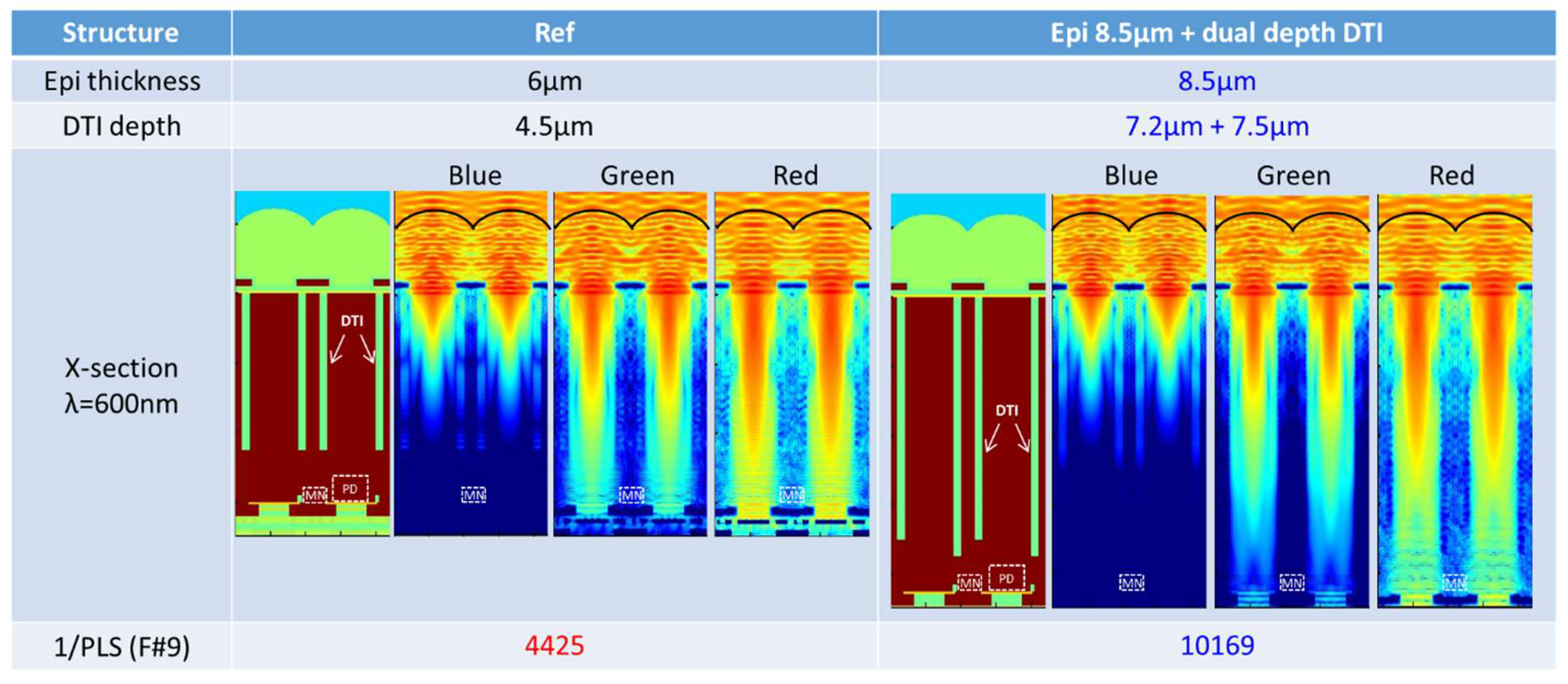
Figure 7.
Key process structure of the dual depth DTI and the alignment mark fabrication.
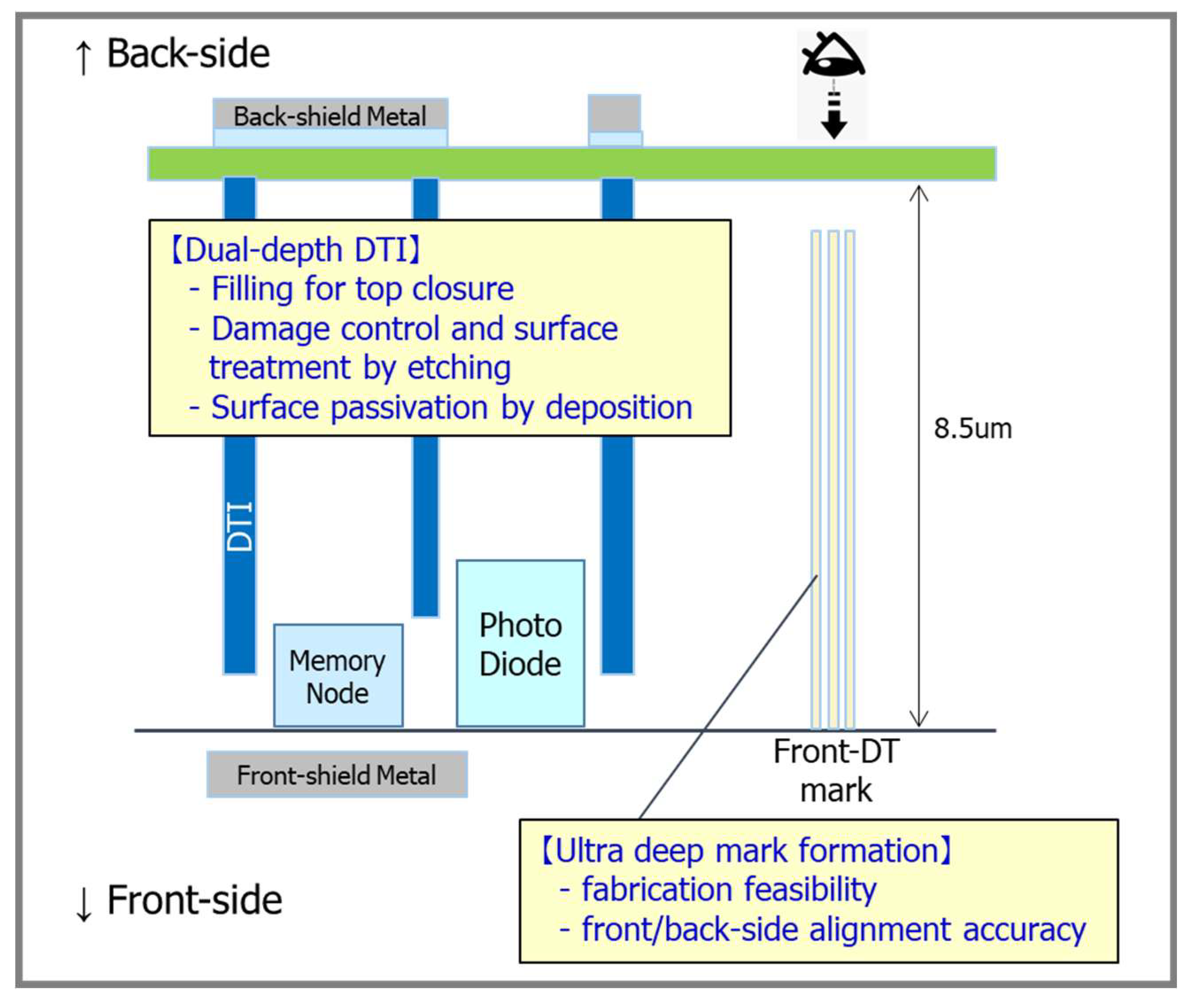
Figure 8.
Cross section of the dual depth DTI.
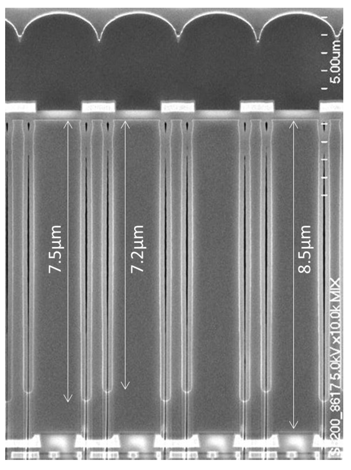
Figure 9.
QE curve (Color & Mono).
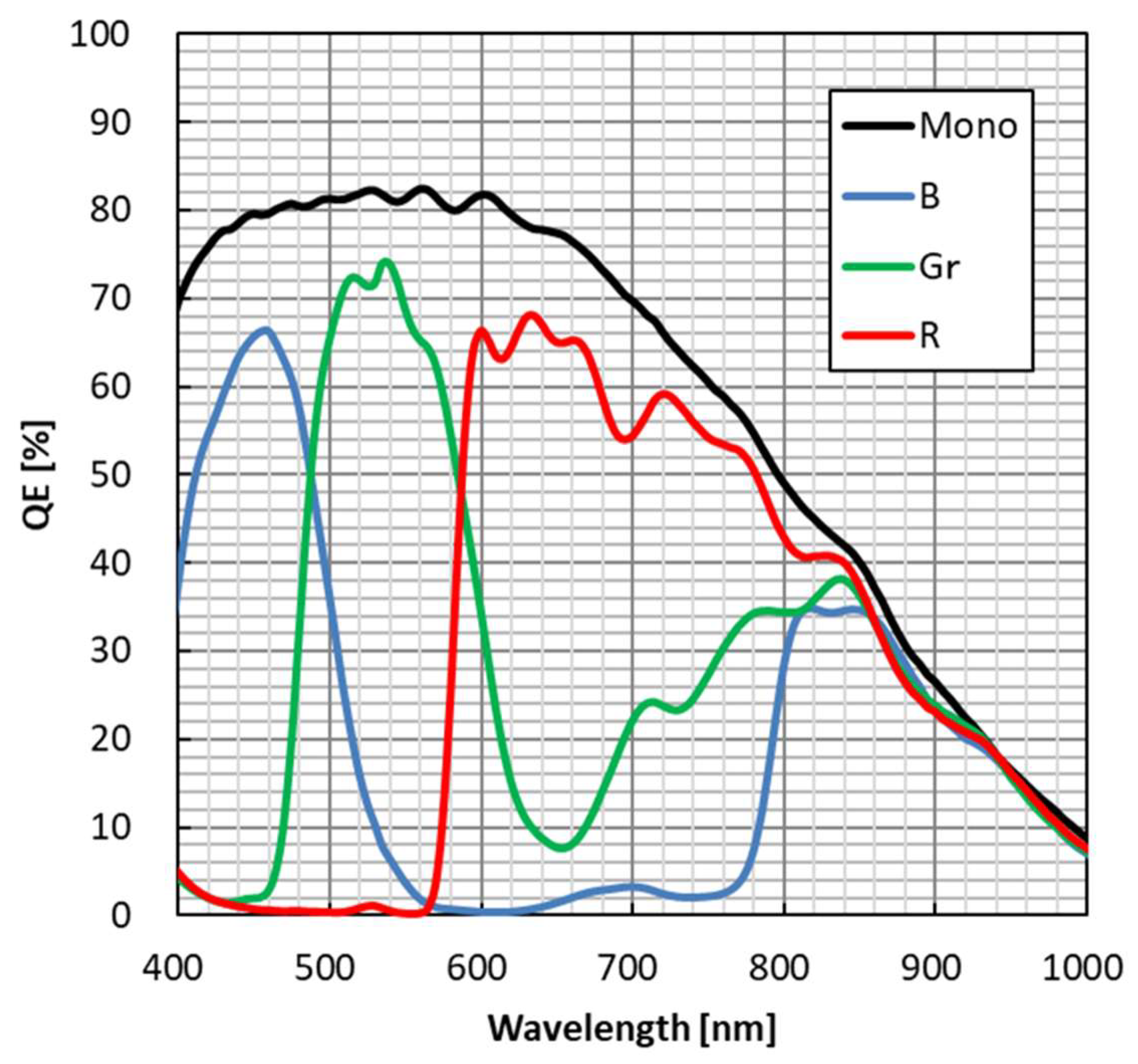
Figure 10.
Wavelength dependence of 1/PLS (Mono).
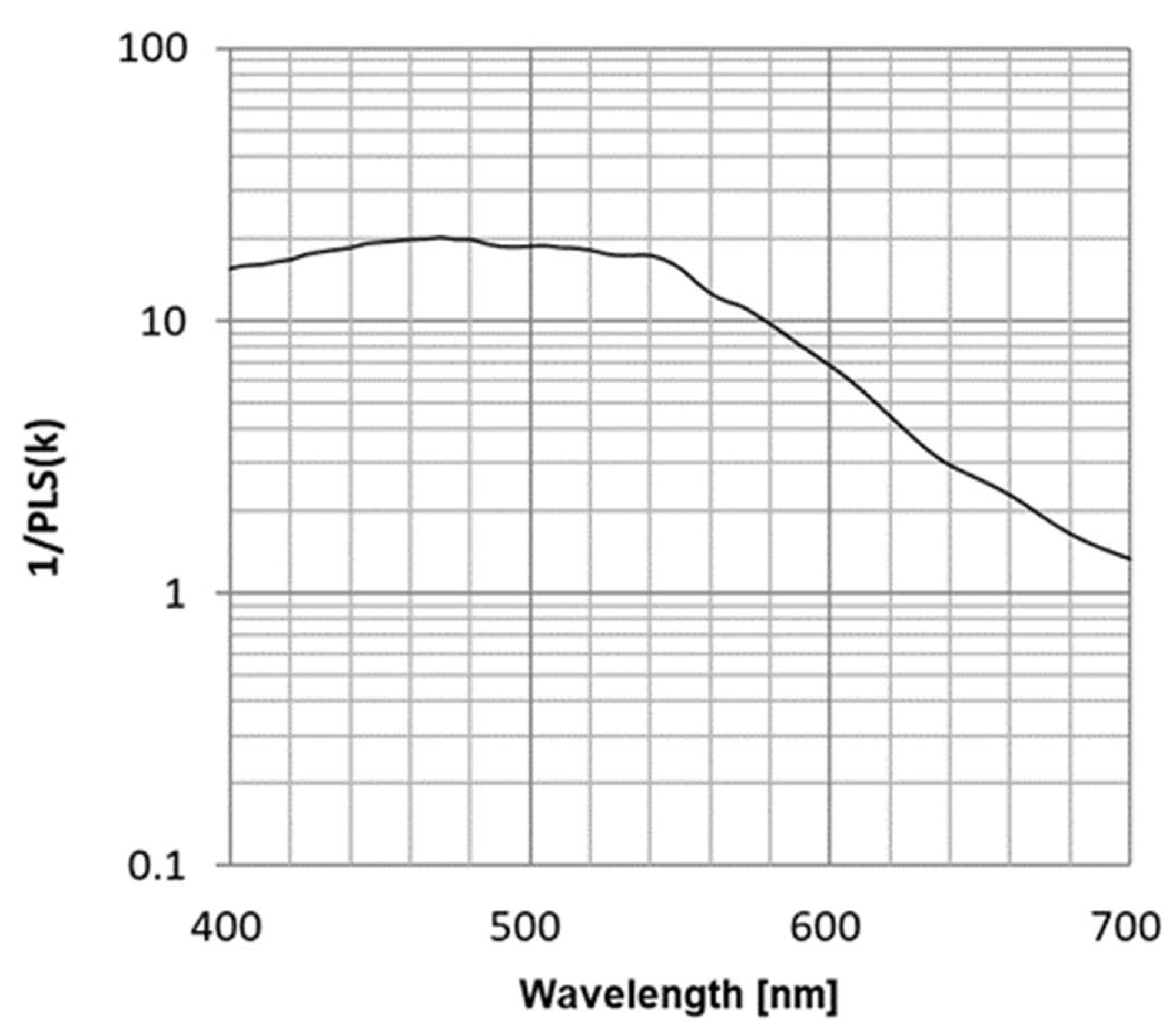
Figure 11.
F#dependence of 1/PLS (Mono).
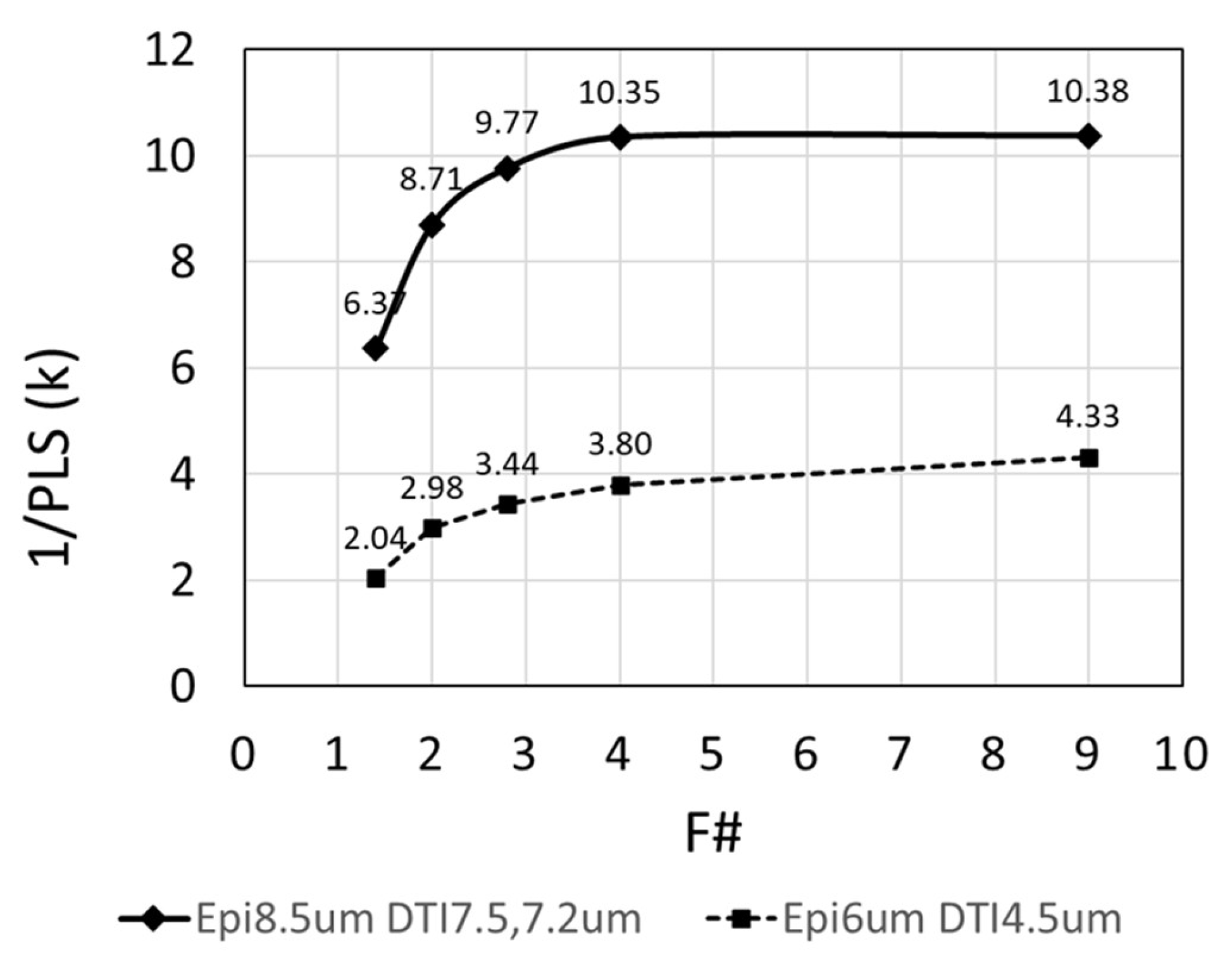
Figure 12.
Angular response of QE.
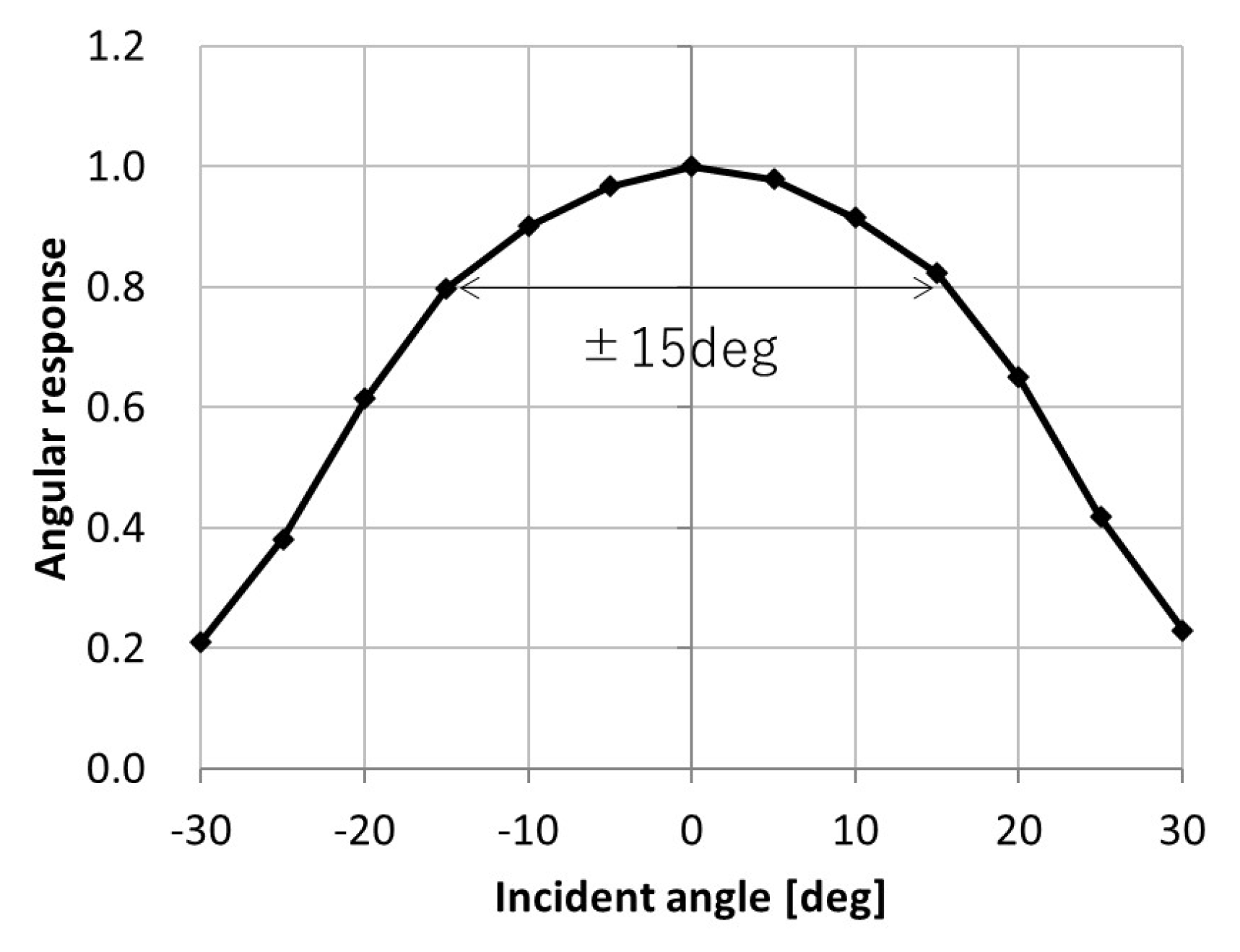
Figure 13.
Comparison of dark current.
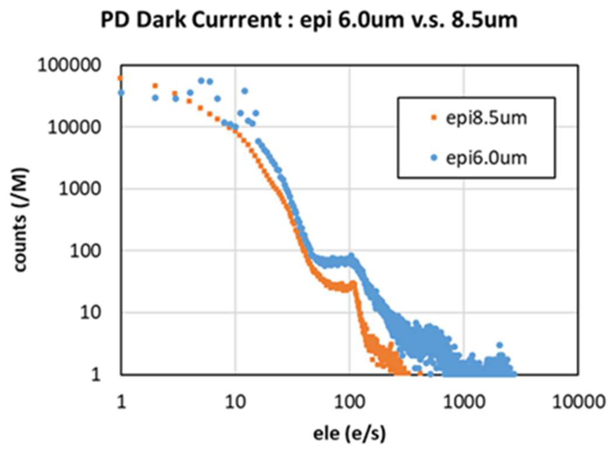

Table 1.
Pixel performance.
| Process Technology | 65nmCIS BSI |
| Pixel Size | 2.2 μm × 2.2 μm |
| Peak QE (Mono) | 83% |
| 1/PLS (F#9, white light, Mono) | 10380 |
| Angular response (80%) | >15 degrees |
| MTF @Nyquist frequency | >40% |
| Linear Full Well Capacity | 5400 ele |
| Pixel noise @SF out (25 deg.C) | 0.6 ele |
Disclaimer/Publisher’s Note: The statements, opinions and data contained in all publications are solely those of the individual author(s) and contributor(s) and not of MDPI and/or the editor(s). MDPI and/or the editor(s) disclaim responsibility for any injury to people or property resulting from any ideas, methods, instructions or products referred to in the content. |
© 2025 by the authors. Licensee MDPI, Basel, Switzerland. This article is an open access article distributed under the terms and conditions of the Creative Commons Attribution (CC BY) license (http://creativecommons.org/licenses/by/4.0/).
Copyright: This open access article is published under a Creative Commons CC BY 4.0 license, which permit the free download, distribution, and reuse, provided that the author and preprint are cited in any reuse.


