Submitted:
01 October 2025
Posted:
02 October 2025
You are already at the latest version
Abstract
VCSEL has aroused extensive enthusiasm in scientific research and applications. However, thermal resistance has seriously limited such devices’ performance for a long time, especially in high-power single-chip large-area VCSEL array module. In addition, thermal resistances of every component of the module are not clear and not exact until now. Here, the thermal characteristics of a 808nm VCSEL module were analyzed by electrical transient measurement, which consists of a 6 mm×6 mm, 85W AlGaAs/GaAs VCSEL array chip encapsulated on a submount and water-cooled heat sink. The authentic and quantitative components of the device’s thermal resistance were clearly segmented and rapidly obtained using the structure function algorithm within merely 25 seconds. The packaging thermal resistance together accounts for astonishing 70% of the total thermal resistance when the loading current is 8 A. Among them, Rsubmount and Rsolder2 are the main focus areas which add up to 54% .We also applied the spectroscopy method to calculate the total thermal resistance of the module from another perspective for the comparative verification of the former method. The values obtained by the two methods are relatively close. More importantly, the research will pose positive significance and indicative effect on reducing main thermal resistances of the VCSEL array module.
Keywords:
VCSEL array module
; thermal resistance
; electrical transient measurement
; structure function
; spectroscopy method
1. Introduction
In recent years, vertical cavity surface emitting laser (VCSEL) has been one of highly promising lasers, which is extensively applied in industry, consumer electronics, medical treatment, military, and so on [1,2,3]. To meet the demand for high-power lasers, single VCSEL array chip with tens of thousands of luminous points within only a few millimeters has been developed in a single chip, which owns laser power from tens to hundreds of watts [4]. However, this also brings a serious heat accumulation problem into the VCSEL array [5]. The situation severely impairs the performance of the VCSEL array such as resulting in increasing threshold current, reducing electro-optical conversion efficiency and impairing working life [6]. So, Thermal resistance analysis is extremely instructive, which is one of the most useful indicators for semiconductor lasers [7,8]. Thermal management for VCSEL array is especially important. However, the exact thermal resistance distribution of the VCSEL array module with cooling is not clear until now [9,10]. The results of finite element simulation are overly idealized and neglect the thermal resistances within the interface transition areas, which leads to the simulation result is usually lower than the actual thermal resistance. In addition, the VCSEL array chip with extremely complex micro/nano architectures is difficult to simulate accurately. Furthermore, simulation consumes a great deal of time even more than several days to calculate [11,12,13]. The electrical measurement technique is a popular method to obtain and analyze the thermal resistance of various power devices such as insulated gate bipolar transistor (IGBT), and so on [14,15,16,17]. More importantly, the method is convenient and accurate. It will not cause any damage to the devices and can obtain the exact distribution of various thermal resistances of the devices under test. However, electrical measurement can not get authentic thermal resistance compositions of the whole module apart from the water cooling part of the module due to limited heat capacity in reality. The spectroscopy method can serve as an important supplementary method to obtain the overall device thermal resistance of the laser module. As stated above, accurate and quantitative thermal resistance analysis in high-power VCSEL array module has a vital role and positive effect on improving its performance.
In this research, we combined electrical transient method and spectroscopy method to quickly and accurately ascertain thermal resistances distribution of the VCSEL array module. First of all, the electrical way is very practical, which is based on the linear relationship between the forward voltage and the semiconductor chip’s junction temperature. By the method, we carefully analyzed the thermal resistance distribution in the VCSEL array module at different loading currents by the structure function method. Then, we applied the spectroscopy method to obtain the total thermal resistance of the module to compare with the aforementioned method. The combination of the two methods is mutually beneficial to dialectically analyze the thermal resistance compositions of the VCSEL array module.
2. Materials and Methods
2.1. Materials Introduction
The 808nm, 6 mm×6 mm, AlGaAs/GaAs top-emitting VCSEL array chip’s main schematic is shown in Figure 1a. The VCSEL array chip is mainly made of P contact electrode layer, P-type distributed Bragg reflector (DBR), oxide aperture, active region, N-type DBR, GaAs substrate, and N contact electrode layer, and so on. The schematic of the VCSEL array module with remote cooling packaging style is shown in Figure 1b.
The module consists of the single VCSEL array chip, the special solder layer 1, the aluminum nitride heat sink submount, the special solder layer 2, and the water cooled heat sink. The packaging form is usually defined as the remote cooling, which is widely used for high-power VCSEL array modules for a long time. Here, the chip with thousands of luminous points is thined to no more than 100μm and then metallized. Nano silver sintering is used between the VCSEL array chip and the submount to ensure no void inside the whole solder layer, which is extremely important. Because the void will cause excessive thermal resistance, which will result in local burning of the VCSEL array. The thickness of the solder layer 1 is merely less than 5μm which is achieved under the process, 20Mpa, 200℃, 90min. At the same time, the solder layer’s thermal conductivity can reach up to 200W/m•K, which is a satisfactory thermal interface. The submount is made of aluminum nitride material which owns thermal expansion coefficient which is similar to gallium arsenide to relieve packaging stress. Double side welding method with indium is used to connect submount and water cooling heat sink. On the one hand, the method is used to reduce voids in the solder layer 2. On the other hand, it also alleviate packaging stress for that indium is so soft which is usually as suitable solder for laser module. The thickness of the solder 2 is about 10μm. The water-cooled heat sink is made of purple copper, which is processed by wire electrical discharge machining to form multi-channel array. By that, we can enhance the ability of convective heat transfer with water or other coolants to dissipate the heat of the module. The channel width of the water cooling heat sink is about 300μm, and the ratio of channel width to wall thickness is about 1:1 in this water-cooled heat sink.
The threshold current of the chip is about 5A. The power/ current/ voltage (PIV) chart is shown in Figure 2, when the module was in continuous wave operation on a water-cooled heat sink, the water temperature was set at around 20℃ and the water flow rate was set at 25L/min to maintain the flow state in turbulence.
The laser power tester was used for laser power detection which is based on the principle of thermo-electric conversion. When the current was set at about 27A, the laser power of the module reached the peak power of about 85W. Then, the output laser power of the module began to decrease due to insufficient heat dissipation of the remote cooling module. To more intuitively reflect the thermal resistance effect of the module, the power conversion efficiency (PCE) curve is shown in Figure 3.
The maximum electro-optic conversion efficiency approached 40% of the module occurs at a loading currents of about 9A~15A. Thereafter, the efficiency started to rapidly decay as the current was gradually loading. As mentioned above, the thermal resistance effect severely limits the electro-optic conversion efficiency of the module. Therefore, detailed thermal resistance analysis of the VCSEL array module is extremely meaningful.
The thermal resistance is a key indicator of thermal performance in semiconductor lasers. The JEDEC standard No.51-1 defines it as [18]:
In this equation(1),refers to the heat dissipation power, refers to the junction temperature of the chip, refers to the ambient temperature. When the VCSEL array is loaded with input current, heat will generate inside the chip and packaging structure, which contains joule heating, scattering absorption, spontaneous emission, carrier leakage, band alignment, and so on. Once the loading current exceeds the threshold current (), the VCSEL array chip will emit laser.
2.2. Structural Function Method
The structural function method for measuring thermal resistance refers to utilizing the linear relationship between the voltage and the temperature of the semiconductor junction. During the heating or cooling process of the semiconductor laser, the transient temperature curve can be obtained by rapidly measuring the junction voltage of the device. With the thermal RC network analysis theory, the transient temperature response curve is analyzed into a thermal RC network, and then transformed into a differential structure function curve by mathematical processing. Thus, a detailed analysis for the thermal resistance of each layer in the device packaging can be well done [19]. Semiconductor devices are generally packaged into multi-layer structures composed of different materials [20]. Within the thermal conduction path of a device, different materials exhibit varying thermal resistances and thermal capacities, leading to distinct temperature responses. Therefore, semiconductor devices and their packaging structures can be regarded as one-dimensional thermal networks. At t=0, we apply heat power to the device, and then the junction voltage of the device is measured to obtain the curve of temperature variation with time during the temperature rise process, which is called the transient response curve. The curve can be equivalent to the response of a Foster RC network model with n units. The response can be expressed as a linear combination of exponential terms with n different time constants:
In the formula (2), represents the thermal response curve,=× is the time constant of the Noi RC, refers to the amplitude coefficient of the exponential term, the time constant spectrum. Real thermal systems exhibit a continuous distribution of time constants expressed in integral form:
Introducing the exponential time variable z=ln t, is expressed as:
For the spectrum of unknown time constants , formula (4) is a devolution type differential equation. Taking the derivative of both sides with respect to z, we obtain:
In the formula (5), W(z)=exp,represents convolution operation. Therefore, after measuring the thermal response curve, it is transformed into an exponential time variable form. Take the derivative of it, then, by performing a deconvolution operation based on equation (5), we can obtain the time constant spectrum of the one-dimensional thermal structure . So, the thermal resistance Ri and thermal capacity Ci in the Foster network can be extracted. In fact, the point-to- point heat capacity in the Foster network has no practical physical significance. Therefore, it is necessary to transform the Foster network into the Cauer network with point to ground thermal capacity model. The N pieces RC units obtained from the Cauer network can be used to approximately describe the heat transfer structures of the device. The thermal response curve of the junction temperature is determined by the structural function of the device. In addition, the structural function is defined as the ratio of heat capacity per unit length to thermal resistance per unit length, that is:
In the formula, x is the linearity of the one-dimensional thermal conduction path.
Along the heat transfer path, we sum up the thermal resistance and heat capacity of each RC unit to get R(x) and C(x). By comparing with them,the distribution of the structural function along the thermal conduction path x can be obtained. In fact, the commonly used structure in thermal resistance test instruments is the differential structure function, which is the function value obtained by differentiating C(x) with respect to R(x):
Considering a thin material with a cross-sectional area of A and a thickness of dx. Its heat capacity can be represented as dC=cAdx. The thermal resistance can be represented as dR=dx/eA. In the formula, c is the volumetric heat capacity. e is the thermal conductivity of the material. Therefore, the differential structure function of equation (7) can be expressed as:
For a certain structure along the heat flow path, both c and e are constants, while the heat flow cross-sectional area A gradually increases due to thermal diffusion effects. There are local peaks or troughs on the curve of the differential structure function. This is caused by the sudden changes in c and e, indicating that the heat flow has reached a new material. Therefore, by analyzing the curve of the differential structure function, we can identify and analyze the internal layer structures of the devices and their thermal conductivity characteristics [20].
The temperature rise and the thermal resistance in the VCSEL array are measured by electrical transient measurement technique. The electrical method is according to the linear relationship between the forward voltage and the junction temperature variation, which is defined as [21]:
is the forward voltage difference of the VCSEL array between before and during operation. means a temperature coefficient. We measured the forward voltages at a steady diminutive current of 1mA under various temperatures from 28℃ to 68℃, in 10℃ per step. The current was loaded with Keithley 2400 source meter, which can keep the stability of the testing data. The ambient temperature was regulated and kept by a constant temperature bath, the temperature tolerance can be controlled within ±0.05℃. Then, we obtained a clear linear proportionality constant, which is about -11mV/℃ at the tiny current of 1mA, as shown in Figure 4.
The thermal resistance of the module was tested by a thermal resistance tester at working currents from 2A to 8A with IT6722A DC power supply, in 2A per step, which is around the threshold current of 5A of the top-emitting VCSEL array chip. The module was set at a stabilized temperature of about 25℃during the thermal transient measurement with a thermostatic bath, as shown in Figure 5.
The laser power was measured by Newport Laser power tester. In addition, the thermal power was acquired by the equation:
means the thermal power. I means the operating current, V means the operating voltage, means the laser power. The VCSEL array was operated at a set current within only 15 seconds, which is enough to keep the device at a steady state. Then, it was quickly switched from just working state to a measurement state to check the forward voltage under a sensor current of only 1 mA. In addition, Due to the fast cooling of the water-cooled module, the cooling time for testing can be completed within merely 10 seconds. The switching process was quick enough within 1μs. With the equation(1) and (9), we can obtain the thermal resistance curve and the transient cooling curve. The transient cooling curve can be switched to a transient temperature rise curve by a mathematical inversion [21,22,23,24]. To get clearer detailed information on the heat conduction process of the module, we analyzed its thermal resistance composition using the transient temperature rise curve with structure function algorithm.
2.3. Spectroscopy Method
The structural function method has considerable advantages in detecting the composition of the module thermal resistance. However, the method has a deficiency in accurately detecting the thermal resistance of the overall water cooling laser module. In this regard, the spectroscopy method is more suitable. GaAs semiconductor lasers are made of direct band gap materials: the junction temperature changes linearly with laser wavelength, which is defined as [25]:
In the above equation, T means the junction temperature variation of the laser chip. λ means wavelength variation. λ(T) means temperature drift coefficient. Firstly, we obtained the temperature drift coefficient by observing the variation of pulse laser wavelength under 5A, 100μs, 100Hz with a stable junction temperature by gradually changing environmental temperature. The ambient temperature was adjusted and controlled by a thermostatic bath instrument shown in Figure 6.
We applied Avantes spectrometer to monitor laser wavelength. Due to the high power of the laser, we used the laser reflection method with a mental plate above to reduce overly intense laser spectral intensity for detection to avoid damaging the instrument. When the temperature was set at constant 25℃, the spectral distribution test is shown in Figure 7, the center wavelength at the low duty cycle is approximately 802.60nm, which is commonly known as cold temperature wavelength. As depicted in Figure 8, the temperature drift coefficient is about 0.056nm/K.
Then, we employed the wavelength drift method to monitor the laser wavelength variation with various operating currents, thereby inferring the junction temperature rise with thermal power, and subsequently calculating the total thermal resistance of the device. To get convenient detection and calculation for the thermal resistance of the laser module, equation (1) can be transformed into the following form [26]:
In the above equation, is the thermal resistance. means the thermal power. We tested the voltage, the laser power, and the wavelength of the VCSEL array module at several different loading currents: 5A~35A, at continuous working condition. These test parameter data are shown in Table 1:
3. Results and Discussion
3.1. The Thermal Resistance Analysis by Structure Function Method
Figure 9 shows the differential structure function of the VCSEL array module at loading current 8 A, and the total thermal resistance of the module is nearly 0.45 K/W. There are four peaks, which respectively correspond to the thermal resistance of the VCSEL array chip, Rchip, the solder layer 1, Rsolder1, the aluminum nitride submount, Rsubmount, the solder layer 2, Rsolder2, and the resistance of the cooling module, Rcooling.
By the differential structure function, we found that every part’s segmented thermal resistance corresponds to the device composition and the thermal resistances are dominated by packaging design. The encapsulation thermal resistances together account for over 70% of the total thermal resistance of the module. The thermal resistance distribution of the module at loading current of 8 A is shown in Figure 10.
Figure 11 similarly shows the cumulative structure function analysis of the VCSEL array module at the same loading current 8 A. This form also plainly presents the thermal resistances accumulation of the module from another perspective. The above analysis facilitates us to carry out the task of reducing thermal resistance with a clear objective.
Methods such as wafer bonding may be an effective approach for reducing interface thermal resistance between the chip and the submount. Furthermore, directly forming the embedded microchannel inside the submount for the module will also effectively reduce the thermal resistances from Rsubmount, Rsolder2, and Rcooling. By the above improvements and efforts, even with a high thermal power density as high as hundreds of kilowatts per square centimeter, the junction temperature of high-power laser chips will be ultimately reduced by our continuous efforts.
3.2. The Thermal Resistance Analysis by Spectroscopy Method
On the other hand, by the data from the differential structure function, we are not able to obtain accurate thermal resistance values about water-cooled heat sink and also the total thermal resistance of the module. Furthermore, in this research, the thermal resistance tester using the structure function algorithm is limited within 10 A, which can not cover the entire the whole current range from 0 A to 35 A. So, we tried to analyze the overall thermal resistance of the VCSEL array module by the spectroscopy method. By the above data from Table 1, we calculated with the equation 10 and the equation 12. Furthermore, we obtained the function among thermal resistance, thermal power and loading current, as depicted in Figure 12.
As the loading current increases, the thermal power of the laser module rapidly increases. The thermal resistance of the laser module is generally between 0.3 K/W~0.5 K/W and not constant along with the chip’s work status. When the current of 15 A was applied, the lowest thermal resistance of the device is approximately 0.27 K/W. Correspondingly, as depicted in Figure 3, the power conversion efficiency reaches a peak range at nearly the same interval. This may stem from two aspects. Firstly, the chip works best in this range. Secondly, the cooling capacity of the packaging structure can effectively control the temperature of the module within this thermal power range. Afterwards, as the thermal power increases, the heat dissipation level of the cooling module became even less able to meet the heat dissipation requirement. The chip junction temperature begins to continuously rise. Then, the module begins to show thermal rollover. This also highlights the importance of changing the packaging structure and improving the heat dissipation level for the VCSEL array module to reduce its thermal resistance effect.
4. Conclusions
The thermal resistances of the 808nm high-power AlGaAs/GaAs VCSEL array module were respectively investigated by electrical transient measurement and spectroscopy method. The quantitative data about thermal resistances values of the module were measured and quickly obtained within less than 0.5 minute. The structure function algorithm was applied to ascertain the quantitative data of the thermal resistance compositions. The results reveal that the total thermal resistance mainly consists of the solders and the submount, which ultimately causes a significant increase in the junction temperature of the VCSEL array chip. The two methods comprehensively explained the influence of thermal resistance on the VCSEL array module from two perspectives. The total thermal resistance of the module is approximately 0.45 K/W and not constant as the chip’s real time mode. When the loading current is 8 A, the packaging thermal resistance accounts for as high as 70% of the total thermal resistance of the module. Rsubmount and Rsolder2 are the main components which add up to about 54% of the total thermal resistance.
The above quantitative analyses will provide accurate results and constructive suggestions for the unremitting efforts to reduce the thermal resistance of the high-power VCSEL module. So, there is a lot of room for optimization in reducing the thermal resistance of the VCSEL array module. The thermal resistances from the Rsubmount and the Rsolder2 are the foci, which need to be significantly reduced. The solder may be replaced by wafer bonding to significantly reduce the Rsolder1. Integrating manifold microchannel cooling within the submount may significantly reduce the thermal resistance of the VCSEL array module.
Author Contributions
Conceptualization, DZ.L.; methodology, DZ.L.; software, DZ.L.; validation, T.L.; formal analysis, T.L.; investigation, T.L.; resources, X.X.; data curation, T.L.; writing—original draft preparation, DZ.L.; writing—review and editing, T.L.; visualization, T.L.; supervision, ZY.Y.; project administration, ZY.Y.; funding acquisition, ZY.W. All authors have read and agreed to the published version of the manuscript.
Funding
This research was funded by the Beijing Natural Science Foundation Program (Grant No.212009).
Institutional Review Board Statement
Not applicable.
Informed Consent Statement
Not applicable.
Data Availability Statement
The original contributions presented in the study are included in the article,further inquiries can be directed to the corresponding author.
Acknowledgments
The authors would like to sincerely thank Avantes corporation for providing technical support and measuring device in testing VCSEL array.
Conflicts of Interest
Not applicable.
References
- Liu J, Zhao F, Tang Z, et al. Advances in high-power vertical-cavity surface-emitting lasers[J]. Journal of Physics D: Applied Physics, 2024, 57(35): 353001. [CrossRef]
- Li Y, Li C, Wei X, et al. High-power 786nm VCSEL-pumped Tm: YAG laser[C]//Solid State Lasers XXXIV: Technology and Devices. SPIE, 2025, 13341: 254-260. [CrossRef]
- Li J Y, Yang J, Wang H, et al. Compact temperature-insensitive high-energy VCSEL side-pumped Nd: YAG laser with a VRM output coupler[J]. Applied Optics, 2025, 64(5): 1134-1138. [CrossRef]
- Lei C, Choquette K D, Zhou D, et al. Progress on high-power high-brightness VCSELs and applications[J]. Vertical-Cavity Surface-Emitting Lasers XIX; SPIE: Bellingham, WA, USA, 2015.
- Wang C, Li C, Wang Z. Analysis of optical and thermal properties of 940-nm vertical-cavity surface-emitting lasers[J]. Optical and Quantum Electronics, 2022, 54(7): 438. [CrossRef]
- Filipchuk A, Nechay K, Ulkuniemi R, et al. Thermal management optimization in high-power 3D sensing VCSELs[C]//Components and Packaging for Laser Systems VIII. SPIE, 2022, 11982: 84-89.
- Wang J, Yuan C, Li Y, et al. Direct-to-chip immersion liquid cooling for high-power vertical-cavity surface-emitting laser (VCSEL)[J]. Applied Thermal Engineering, 2025, 269: 126137. [CrossRef]
- Yuan C, Li Y, Wang Y, et al. Thermal management of high-power vertical-cavity surface-emitting laser arrays[J]. IEEE Transactions on Electron Devices, 2023, 70(12): 6421-6426. [CrossRef]
- Seurin J F, Xu G, Miglo A, et al. High-power vertical-cavity surface-emitting lasers for solid-state laser pum**[C]//Vertical-Cavity Surface-Emitting Lasers XVI. SPIE, 2012, 8276: 64-73.
- Filipchuk A, Nechay K, Ulkuniemi R, et al. Thermal management optimization in high-power 3D sensing VCSELs[C]//Components and Packaging for Laser Systems VIII. SPIE, 2022, 11982: 84-89.
- Mimura M, Miyamoto T. Thermal conductivity reduction effect of thin layer on thermal resistance of vertical cavity surface emitting lasers[J]. Japanese Journal of Applied Physics, 2018, 57(8S2): 08PD02. [CrossRef]
- Qi Y, Li W, Liu S, et al. Optimized arrangement of vertical cavity surface emitting laser arrays to improve thermal characteristics[J]. Journal of Applied Physics, 2019, 126(19). [CrossRef]
- Namvar B, Uusitalo T, Virtanen H, et al. Improving p-doped DBRs operation at cryogenic temperatures: Investigating different mirror geometry[J]. IEEE Photonics Journal, 2024, 16(4): 1-9. [CrossRef]
- Wang Q, Zhou Y, Lu X, et al. Thermal resistance optimization of GaN-on-Si materials for RF HEMTs based on structure function method and static-pulsed I–V measurements[J]. Applied Physics Letters, 2025, 126(14). [CrossRef]
- Guo C, Cui S, Tsai W, et al. Measuring double-sided thermal resistance of press-pack IGBT modules based on ratio of double-sided heat dissipation[J]. IEEE Transactions on Electron Devices, 2023, 70(4): 1776-1781. [CrossRef]
- Górecki P, Górecki K, Kisiel R, et al. Investigations of an influence of the assembling method of the die to the case on thermal parameters of IGBTs[J]. IEEE Transactions on Components, Packaging and Manufacturing Technology, 2021, 11(11): 1988-1996. [CrossRef]
- Hwang W J, Lee T H, Choi J H, et al. Thermal investigation of GaN-based laser diode package[J]. IEEE Transactions on components and packaging technologies, 2007, 30(4): 637-642. [CrossRef]
- Electronic Industries Association.Integrated circuit thermal measurement method-electrical test method.EIA/JEDEC Standard, JESD51-1,1995.
- Feng S, Xie X, Lu C, et al. The thermal characterization of packaged semiconductor device[C]//Sixteenth Annual IEEE Semiconductor Thermal Measurement and Management Symposium (Cat. No. 00CH37068). IEEE, 2000: 220-226.
- Székely V, Van Bien T. Fine structure of heat flow path in semiconductor devices: a measurement and identification method[J]. Solid-state electronics, 1988, 31(9): 1363-1368.
- Yuezong Z, Shiwei F, Xuesong X, et al. Study of thermal characteristics of semiconductor light-emitting devices[J]. Journal of Semiconductors, 2006, 27(2): 350-353.
- Feng M X, Zhang S M, Jiang D S, et al. Thermal characterization of GaN-based laser diodes by forward-voltage method[J]. Journal of Applied Physics, 2012, 111(9).
- Zhang G C, Feng S W, Zhou Z, et al. Evaluation of thermal resistance constitution for packaged AlGaN/GaN high electron mobility transistors by structure function method[J]. Chinese Physics B, 2011, 20(2): 027202.
- Shieh, Brian, et al. "Empirical Modeling and measurement of the Pulsed Junction Temperature of VCSEL." 2019 20th International Conference on Electronic Packaging Technology (ICEPT). IEEE, 2019. [CrossRef]
- Liu X, Wang J, Wei P. Study of the mechanisms of spectral broadening in high power semiconductor laser arrays[C]//2008 58th Electronic Components and Technology Conference. IEEE, 2008: 1005-1010. [CrossRef]
- Jimenez J, Tomm J W. Spectroscopic Analysis of optoelectronic semiconductors[M]. Switzerland: Springer, 2016.
Figure 1.
(a) Main schematic of VCSEL array chip (b) Schematic of VCSEL array module.
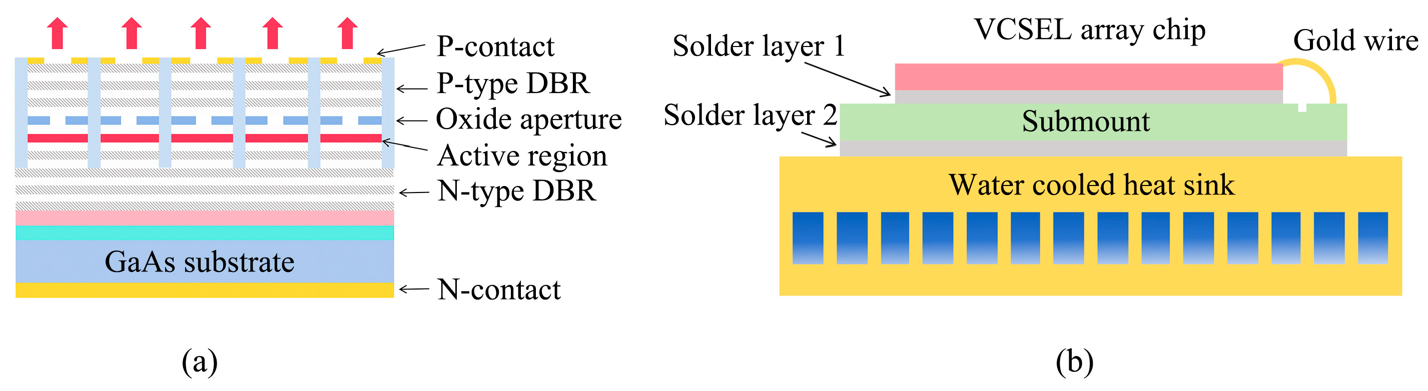
Figure 2.
PIV curve of the VCSEL array module .
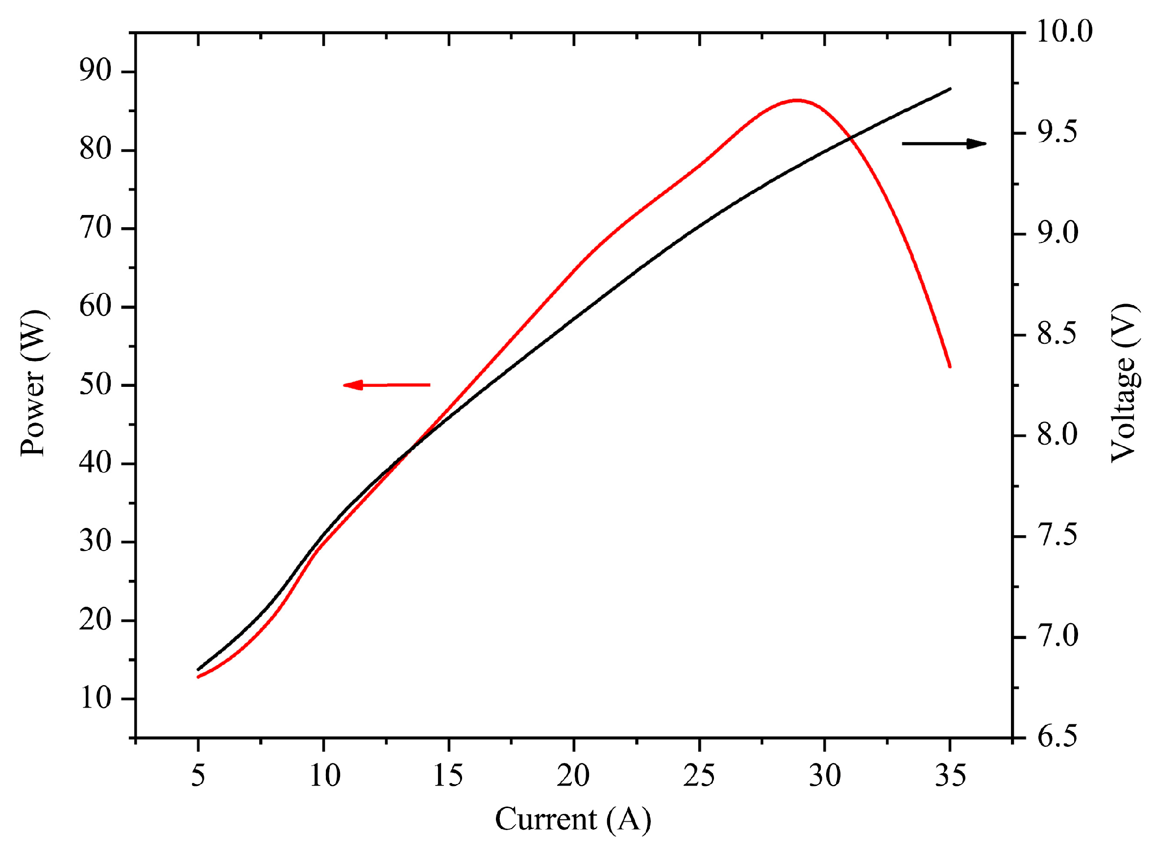
Figure 3.
Power Conversion Efficiency (PCE) curve of the VCSEL array module.
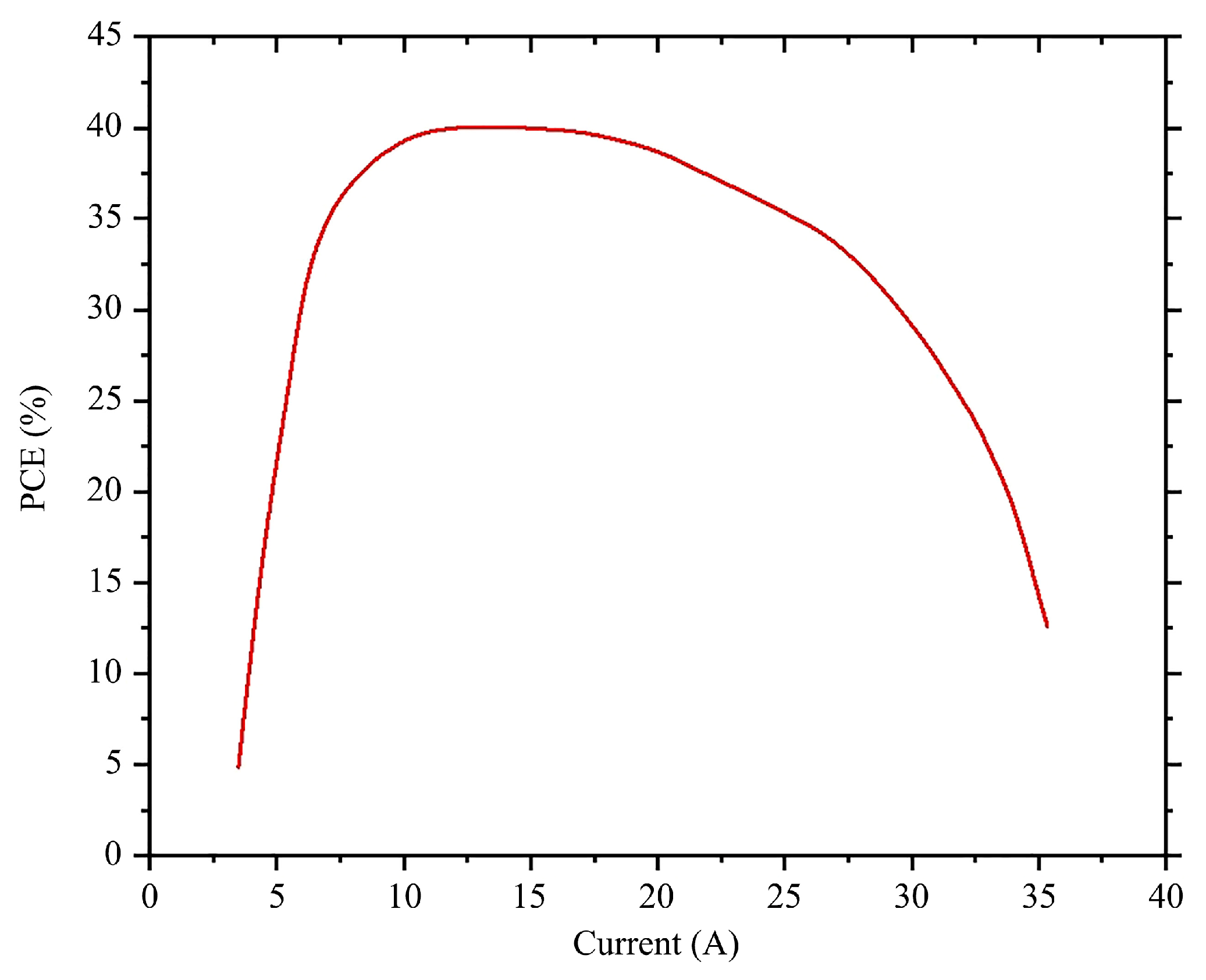
Figure 4.
Forward voltage as function of temperature.
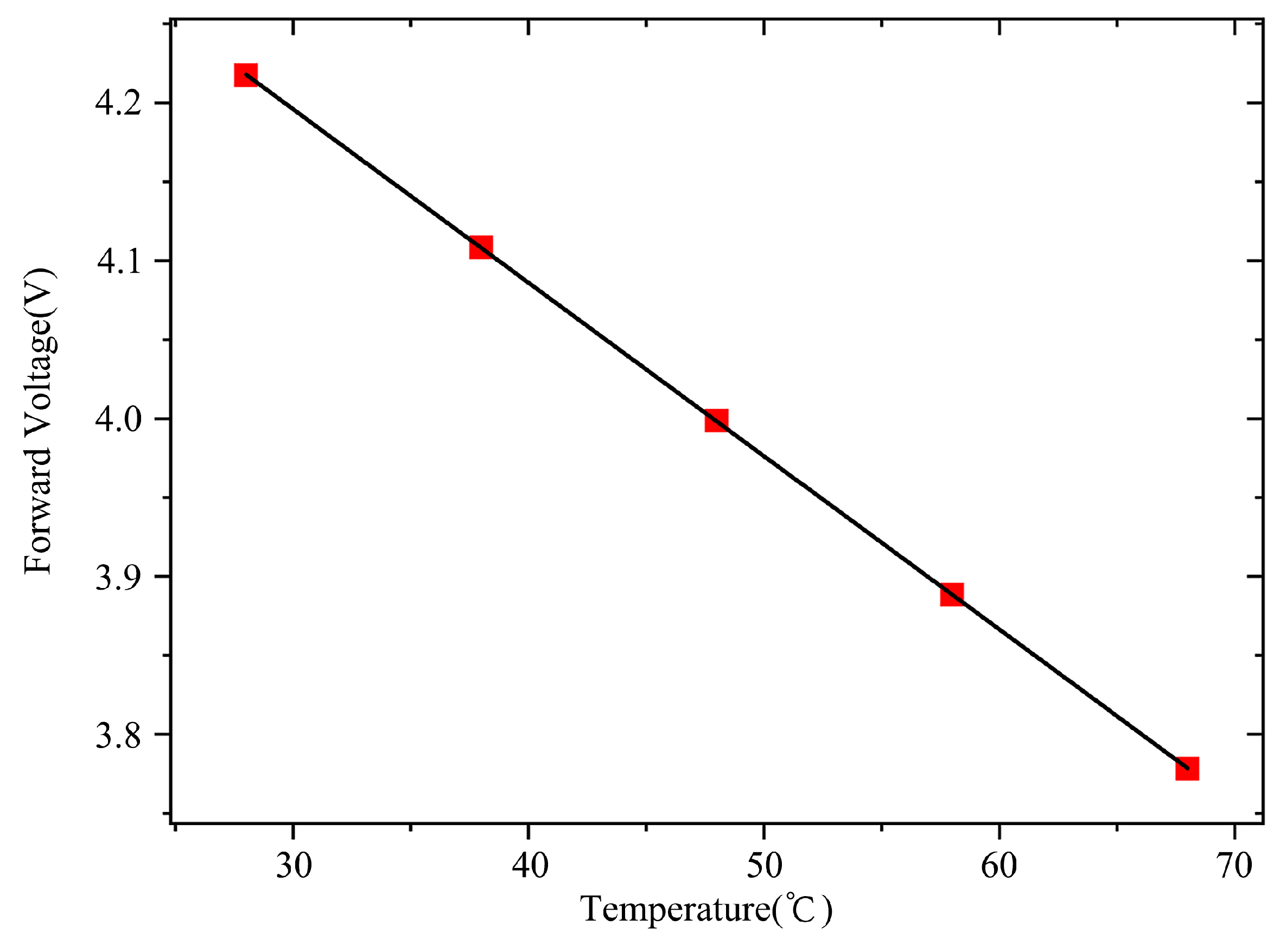
Figure 5.
Thermal resistance testing system.
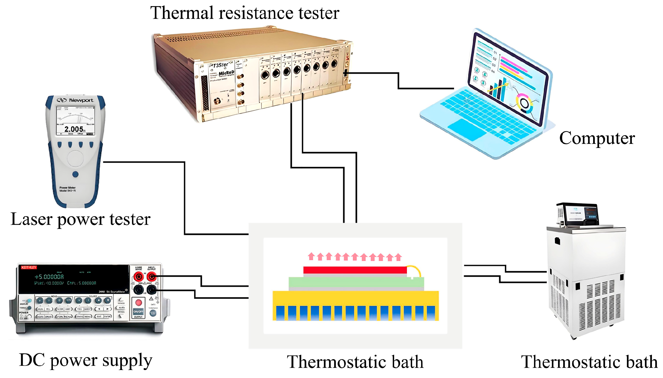
Figure 6.
Spectroscopy method testing system.
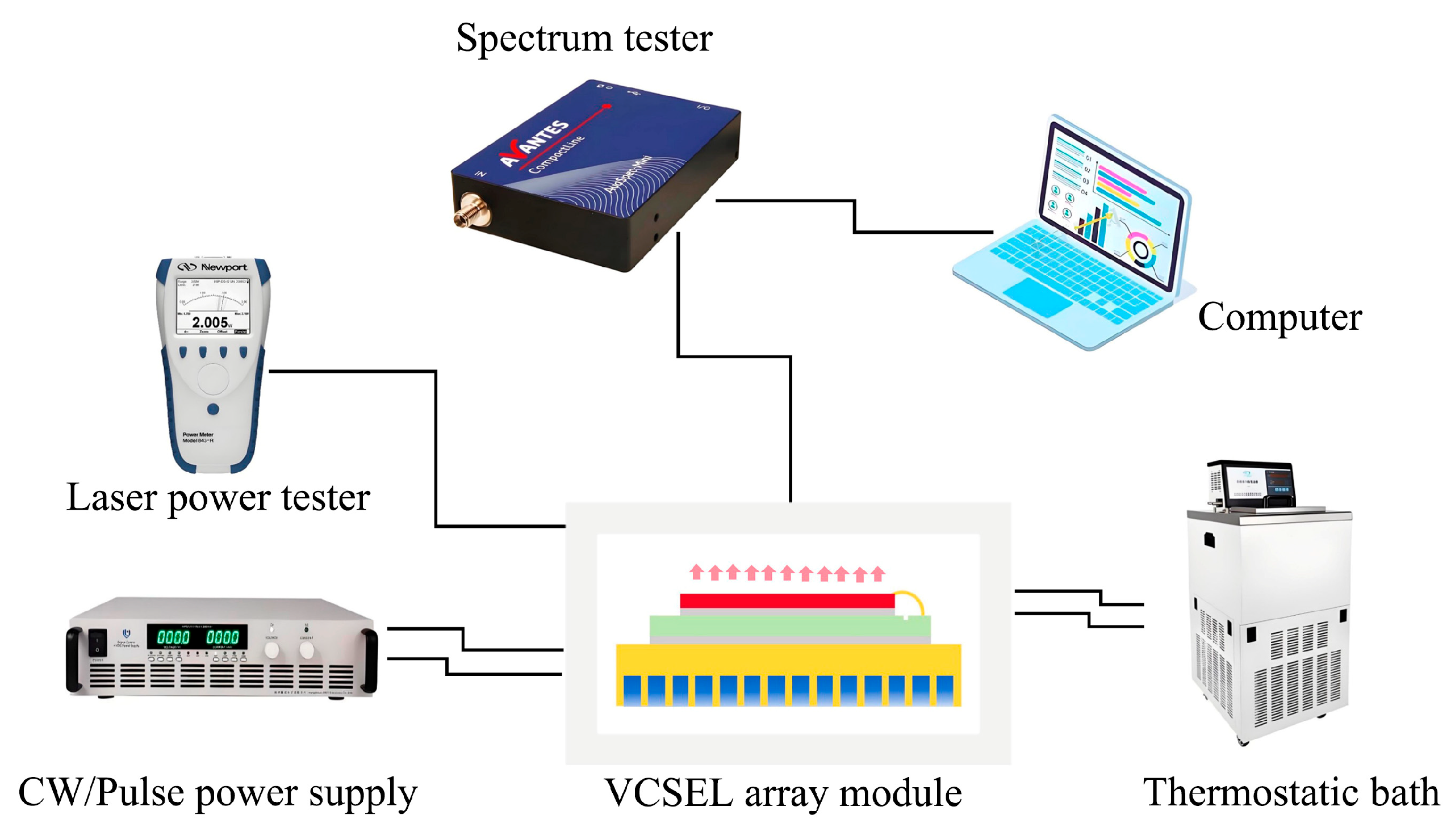
Figure 7.
Spectral distribution at 25℃ and low duty pulse working state.
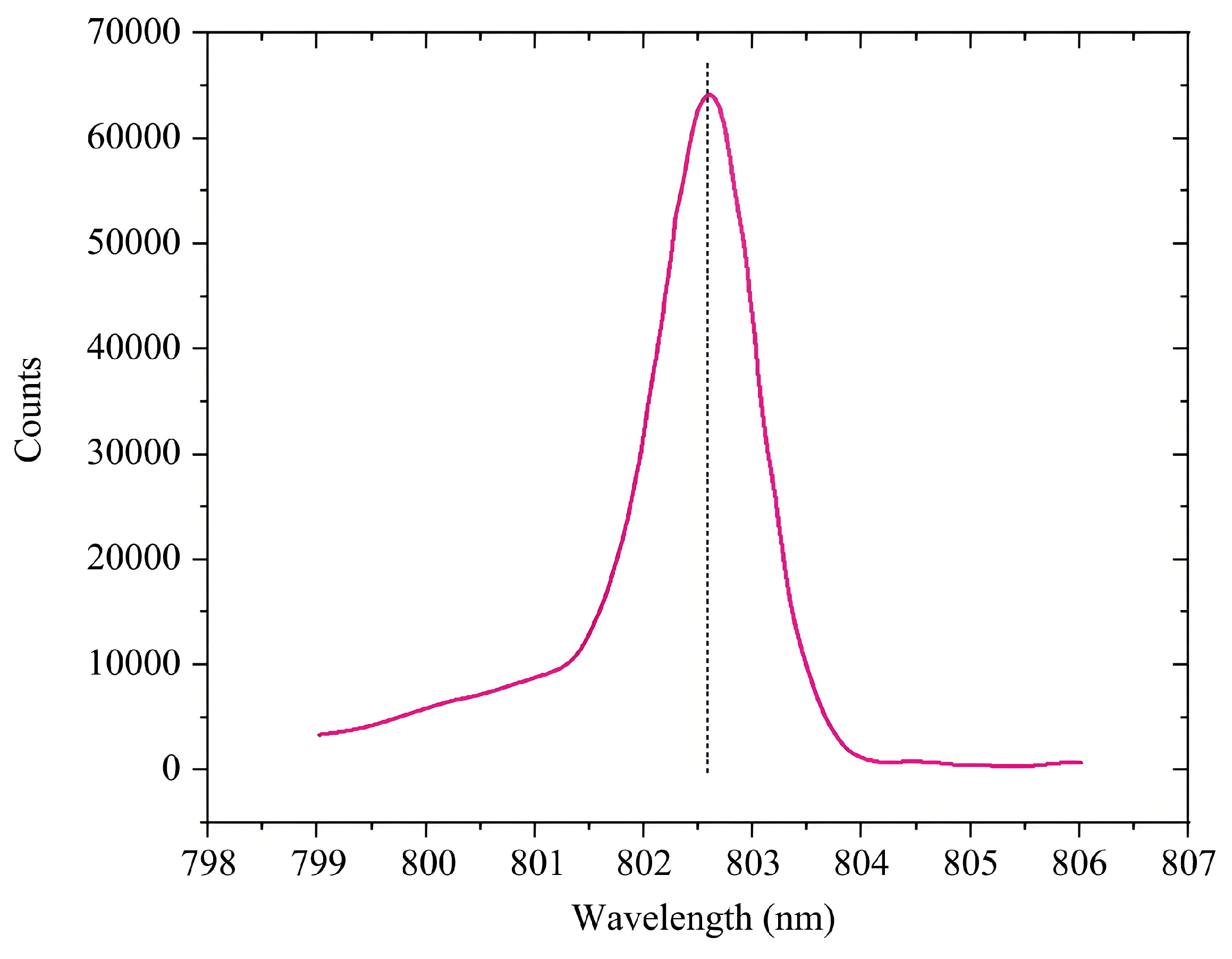
Figure 8.
Wavelength as function of the temperature.
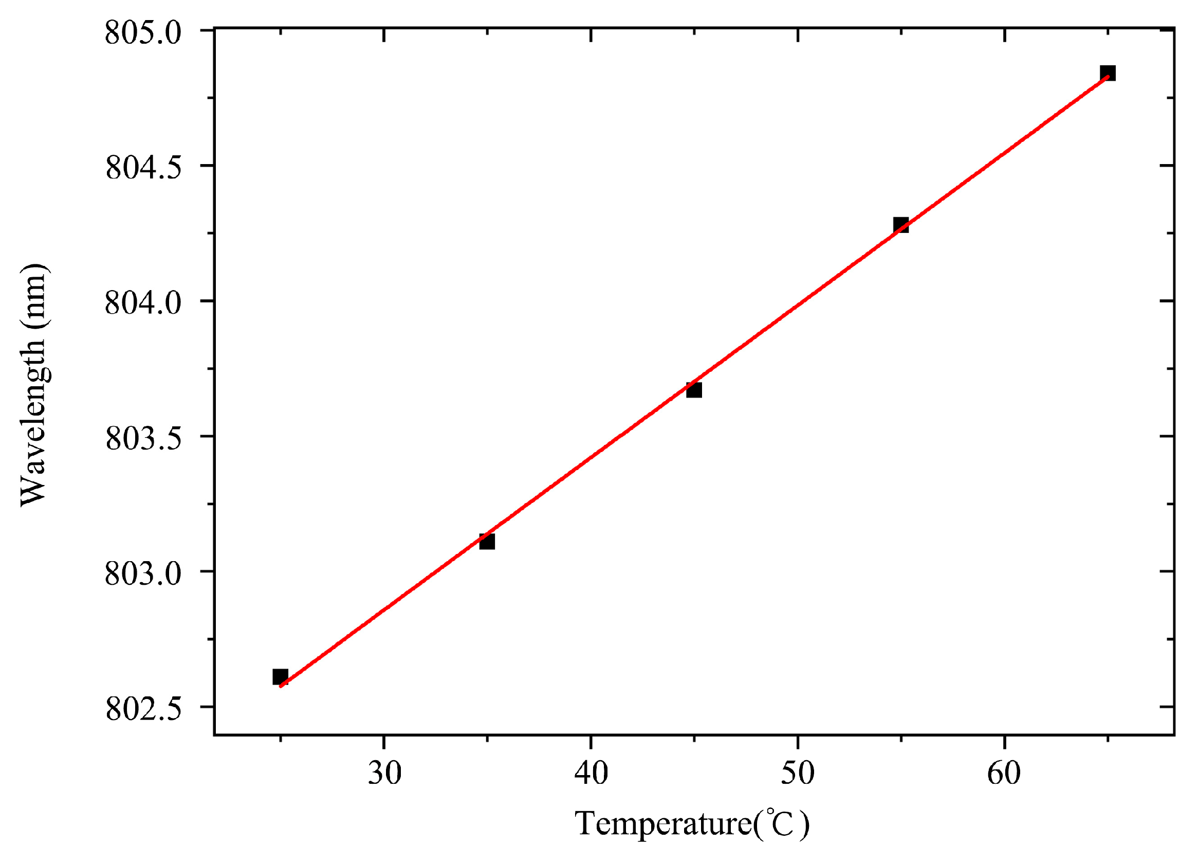
Figure 9.
Differential structure function at loading current 8A.
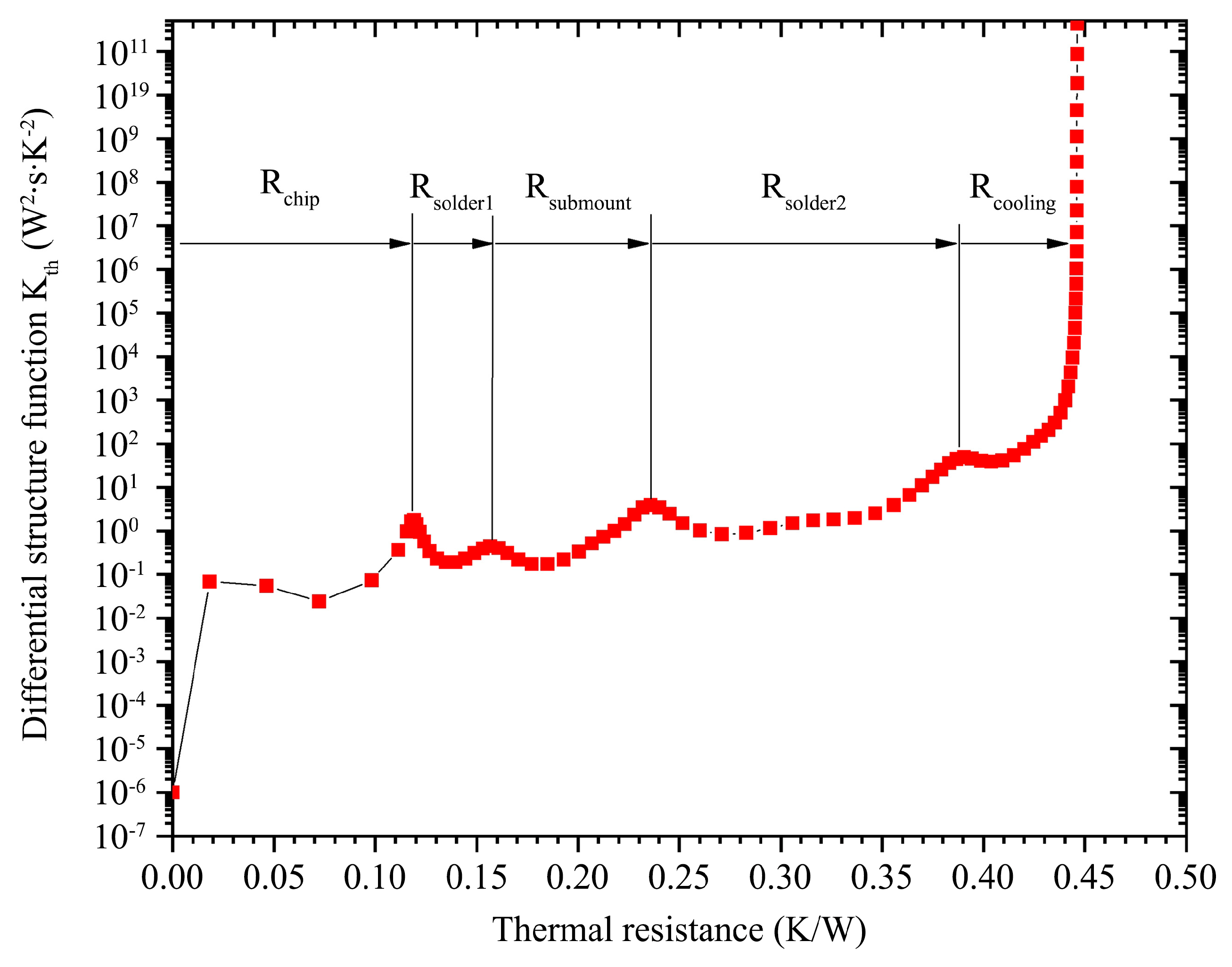
Figure 10.
Thermal resistances distribution of the module at loading current 8 A.
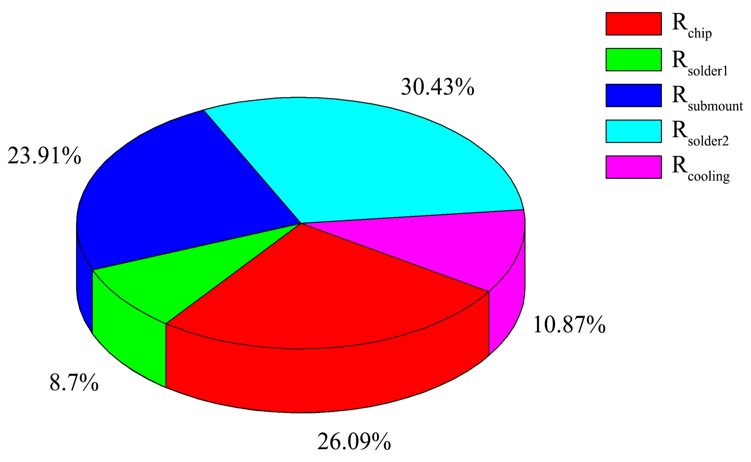
Figure 11.
Cumulative structure function at loading current 8A.
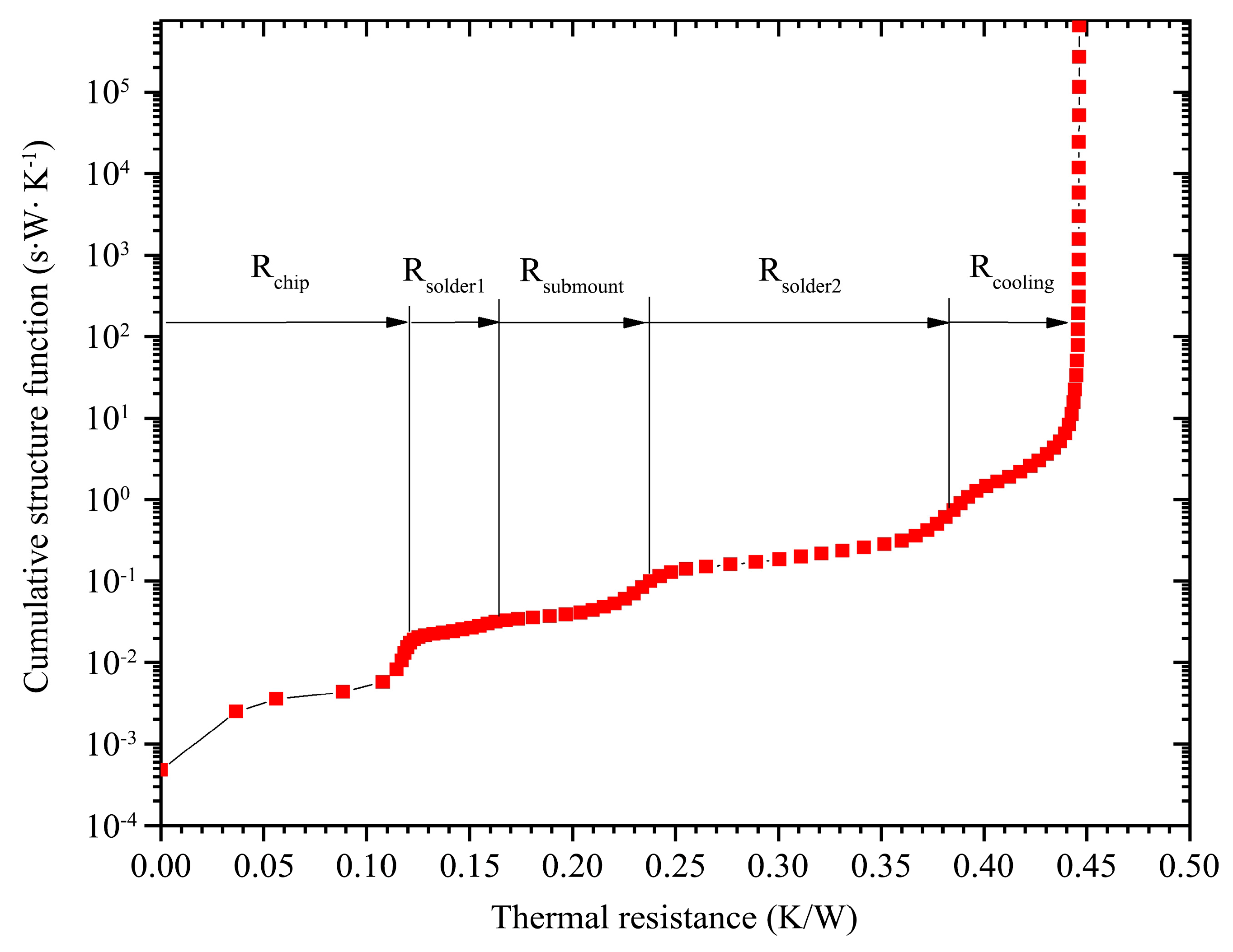
Figure 12.
Thermal resistances and thermal powers as function of various loading currents .
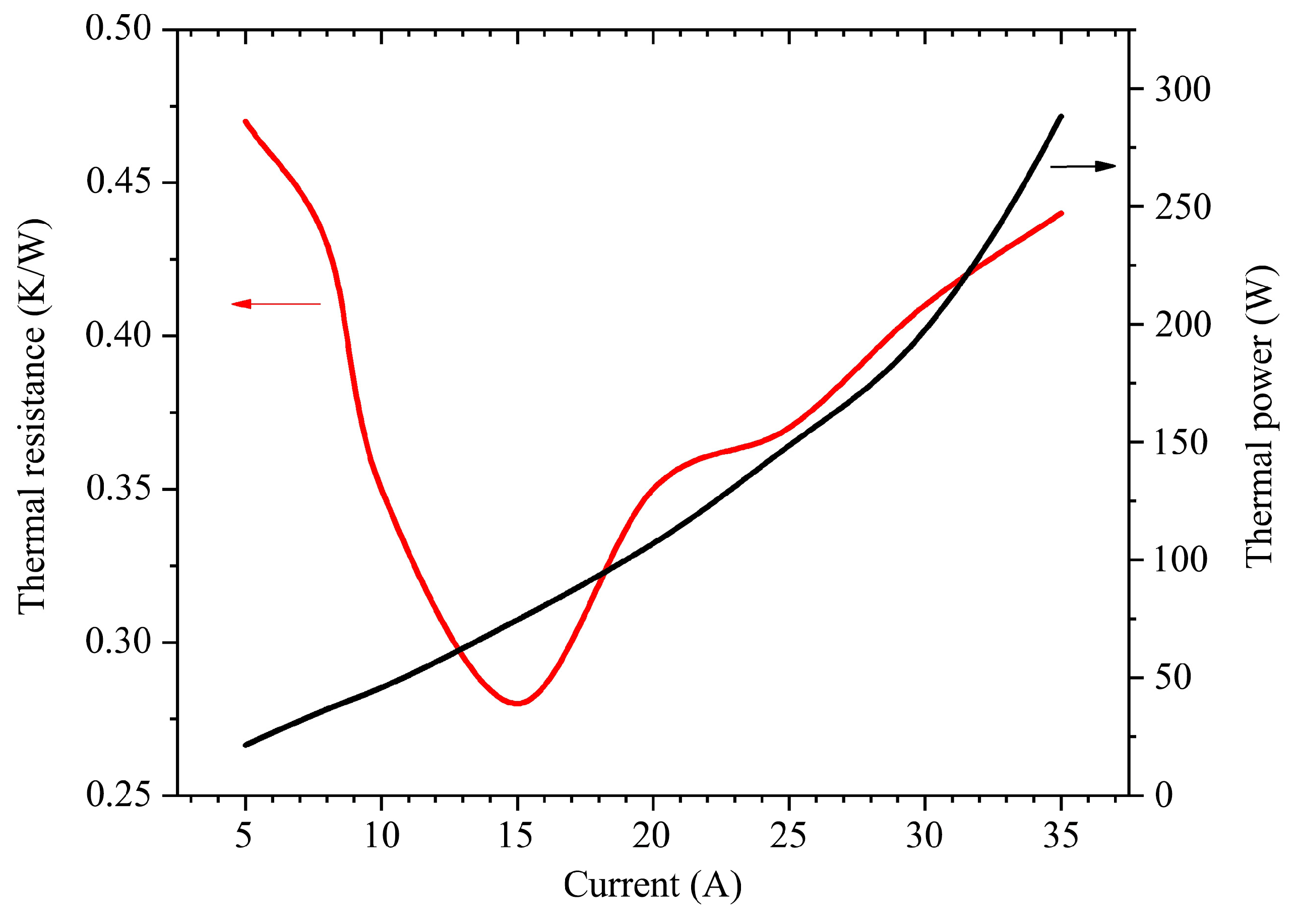

Table 1.
Test parameter data of the VCSEL array module.
| Current(A) | Voltage(V) | Laser power(W) | Wavelength(nm) | Thermal power(W) |
|---|---|---|---|---|
| 5 | 6.84 | 12.8 | 803.16 | 21.4 |
| 8 | 7.14 | 20.5 | 803.41 | 36.6 |
| 10 | 7.56 | 29.8 | 803.50 | 45.8 |
| 15 | 8.10 | 47.0 | 803.78 | 74.5 |
| 20 | 8.58 | 64.6 | 804.67 | 107.0 |
| 25 | 9.06 | 82.2 | 805.90 | 144.3 |
| 30 | 9.42 | 85.0 | 807.13 | 197.6 |
| 35 | 9.72 | 52.4 | 809.58 | 287.8 |
at continuous working condition.
Disclaimer/Publisher’s Note: The statements, opinions and data contained in all publications are solely those of the individual author(s) and contributor(s) and not of MDPI and/or the editor(s). MDPI and/or the editor(s) disclaim responsibility for any injury to people or property resulting from any ideas, methods, instructions or products referred to in the content. |
© 2025 by the authors. Licensee MDPI, Basel, Switzerland. This article is an open access article distributed under the terms and conditions of the Creative Commons Attribution (CC BY) license (http://creativecommons.org/licenses/by/4.0/).
Copyright: This open access article is published under a Creative Commons CC BY 4.0 license, which permit the free download, distribution, and reuse, provided that the author and preprint are cited in any reuse.


