Submitted:
22 September 2025
Posted:
23 September 2025
You are already at the latest version
Abstract
Aerogels represent an extraordinary class of materials characterized by remarkable properties, including an exceptionally high porosity (approximately 99.8%), minimal weight, extraordinarily low density, low thermal conductivity, a diminished dielectric constant, and a reduced refractive index. These attributes arise from their extensive micro-meter-sized pores. In recent years, there has been a notable surge of interest in carbon or carbon nanotube (CNT) based aerogels due to their compelling potential across various applications, encompassing sensors, energy systems, and catalysis, among others. In the context of our ongoing investigation, we have successfully synthesized lightweight aerogels by incorporating copper and carbon nanotubes (Cu-CNT) through electrospinning. Intriguingly, these aerogels exhibit an electrical conductivity of approximately 0.5x10³ S/cm, positioning them within the realm of semiconductors. Concurrently, their density measures approximately 1.669 g/c.c (similar to CNTs), underscoring their notably low mass. These semi-conductive aerogels, uniquely characterized by their lightweight nature and expansive surface area (approximately 442 m2/g), manifest considerable potential across a spectrum of applications. This includes catalytic processes, energy storage mechanisms, bio-sensing technologies, thermoelectric systems, and the burgeoning domains of micro and wearable electronics. The distinctive combination of properties within these aerogels augments their suitability for these diverse applications, offering the prospect of innovative and impactful advancements in various scientific and technological arenas.
Keywords:
electrospinning
; carbon nanotubes-CNTs
; aerogels
; electrical conductivity
1. Introduction
Aerogels stand as a distinctive category of porous gel materials, wherein the liquid component is replaced by air, preserving the material’s shape without any reduction in size. They can be likened to foams, exhibiting a diversity of shapes and sizes. Notably, aerogels boast a multitude of exceptional traits, including high porosity, minimal thermal conductivity, remarkably low density, a diminished dielectric constant, and a reduced refractive index, making them exceptional among dense man-made materials. The structure of an aerogel is characterized by an intricate network of branched structures, forming an exceedingly porous framework with nanometer-scale dimensions. These exceptional attributes render aerogels applicable across a wide spectrum of potential uses[1,2].
The majority of aerogels have been synthesized using either silica [1] or pyrolyzed organic polymers [3]. Silica aerogels garnered interest for their structural, radiation-detecting, and thermal insulating properties, while pyrolyzed polymers found applications in battery electrodes and supercapacitors [3].Despite being technically categorized as foams, aerogels can manifest in diverse shapes and hierarchical structures. Notably, carbon, iron oxide, semiconductor nanostructures, gold, and copper can also yield aerogels, as illustrated in Figure 1. For instance, Cao et al. synthesized silica and titania-silica (TiO2-SiO2) aerogels boasting ordered and disordered mesopores [4]. These aerogel blocks displayed permeability and exhibited a transition-regime diffusion behavior. Enhanced titanium content led to pore and volume shrinkages, resulting in diminished flux. Similarly, lightweight vanadium aerogels were formulated via nanocasting of an isocyanate-derived polymer onto a complex worm-like skeletal framework[5]. These vanadium aerogels exhibit promise as ideal materials for thermal insulation and impact protection in contexts like liquid hydrogen storage tanks, vehicles, and personal armor for impact protection. Diverse aerogels have been reported, including those based on alumina Al2O3[6], various metal oxides (CeO2, Pr2O3, Nd2O3, Al2O3, Ga2O3, Fe2O3, ZrO2) [7,8] , oxides (CO2), and sulfides (CdS) [9] , along with complex oxides such as TiO2-SiO2 and Fe2ZnO4 [4,10] . However, these fabrication methods often necessitate controlled conditions like pressure drying, cross-linking, and supercritical drying. Furthermore, while carbon-based aerogels can be derived from organic polymers like polybenzoxazine, and pure silica aerogels are prone to brittleness and cracking.
To address these limitations, the incorporation of small-diameter carbon nanotubes (CNTs) emerges as an exciting avenue for conductive aerogels, as CNTs offer mechanical stiffness and enhanced electrical conductivity[11,12]. Additionally, CNT-based composite aerogels form electrically percolating networks through van der Waal interactions, even at very low volume fractions[13,14]. Electrospinning, a promising method for producing nanofibers, offers a means to enhance conductive metal-CNT (Cu-CNT) aerogels through structural and mechanical synergies. This paper introduces a novel approach involving electrospinning to create Cu-CNT-based aerogels with expansive surface areas and highly interconnected networks. Electrospinning harnesses the potential of Cu-CNTs to amplify structural and mechanical attributes. Specifically, small-diameter CNTs (SWCNTs and MWCNTs) are chosen due to their exceptional nanotube-level conductivity [12,13]. Assemblies of these nanotubes serve as valuable aerogel precursors, forming electrically percolating networks even at minute volume fractions [14] and remaining elastic in concentrated suspensions through van der Waals interactions [15,16].
2. Materials and Methods
Materials
Poly(vinylpyrrolidone) (PVP) with a molecular weight of 1.3 × 10^5, Copper (II) sulfate pentahydrate (CuSO4·5H2O), and Single-Walled Carbon Nanotubes (SWCNTs) were procured from Sigma Aldrich. The SWCNTs, known as P3-SWCNT, possess a purity exceeding 90% and a metal content ranging from 5-7 wt%. Methanol of analytical reagent grade was obtained from Thermo Fisher Scientific in Singapore.
Sample Preparation
A total of 0.6 g of Copper (II) sulfate pentahydrate (CuSO4·5H2O) with a 60% concentration was combined with 0.75 mL of Methanol and subjected to stirring for a duration of 5 hours. Simultaneously, in a separate sample vial, 0.005 g of Single-Walled Carbon Nanotubes (SWCNTs) with a 0.15% concentration was mixed with 0.25 mL of Methanol and subjected to continuous stirring for an equivalent period of 5 hours. Subsequently, 0.05 g of Poly(vinylpyrrolidone) (PVP) at a concentration of 5% was introduced into the vial containing the SWCNTs, and the stirring was sustained for an additional 3 hours. Once a clear solution was achieved, the solution containing SWCNTs was amalgamated with the CuSO4·5H2O solution, and the combined mixture was subjected to stirring for an additional 5 hours.
Electrospinning of Cu/CNT Aerogel
The Cu-SWCNTs solution was employed for the process of electrospinning[27,28,29]. To facilitate this, a 3 mL syringe with an 18G needle was employed for loading the solution. The flow rate was set at 0.8 mL/h, and the distance between the rotating substrate and the needle’s tip was maintained at 12 cm. A voltage of 25 kV was applied between the two electrodes. Throughout the electrospinning process, the humidity level within the electrospinning chamber was carefully maintained at approximately 50%. The resultant electrospun fibers, characterized by their uniformity, were collected on an aluminum substrate. To eliminate any residual solvent within the fibers, they underwent vacuum drying for a duration of 12 hours. Subsequently, the fibers were contorted into a wired configuration [30] . To ensure stability, these electrospun wires were subjected to an air oven at 100°C for a period of 1 hour. Following this, the temperature gradually elevated to 450°C at a rate of 1°C per minute, a step designed to eliminate the polymer present within the fibers. Despite these treatments, the Cu-CNT fibers retained their CuO-CNT composition. A subsequent annealing step was performed at 600°C for 2 hours within an air atmosphere. This step involved a ramp rate of 5°C per minute. It is anticipated that this annealing process will induce the transformation of continuous fibers into diverse porous structures through calcination.
3. Results
Surface Morphology and EDX Analysis
The microstructures and nanostructures were examined using scanning electron microscopy (SEM), specifically the JSM-6701 model from Asia Pte. Ltd. The morphologies obtained have been illustrated in Figure 2. In Figure 2 (a & b), it is discernible that porous structures are evident, showcasing an effective interconnectivity between particles. Impressively, the original fiber shapes have been preserved. Moving to Figure 2c, the imagery reveals that the carbon nanotubes (CNTs) are seamlessly embedded within the copper (Cu) particles, and a cohesive physical association between Cu and CNTs is evident. Figure 2d provides an Energy Dispersive X-ray Spectroscopy (EDS) representation, confirming the presence of copper. It is noteworthy that these distinctive porous formations have been christened as Cu-CNT aerogels, aptly capturing their composition and unique characteristics.
Crystal Structures
The crystal structures of the electrospun Cu-CNT aerogels were subjected to characterization through powder X-ray diffraction (XRD), utilizing Cu Kα (1.5406 Å) radiation within a 2θ range spanning from 20° to 80°. As demonstrated in Figure 3, distinct and well-defined peaks emerge at 42.6°, 50.3°, and 72.5°, corresponding to diffractions originating from the (111), (200), and (220) planes of copper, as per the JCPDS reference code 04-836. These diffraction peaks align with the distinctive face-centered cubic (FCC) copper peaks [31]. Additionally, a sharply defined peak at 29.0° corresponds to the (002) plane of carbon nanotubes (CNTs).
Notably, the Cu (200) peak is employed for the purpose of estimating the surface area (Sa), which is calculated using the formula Sa = 6 / (dhkl * ρ) [30]. Here, ρ represents the density and is given by the equation ρ = (nM / NV), where n stands for the number of atoms within the unit cell, M signifies the molecular weight, N denotes Avogadro’s number, and V signifies the volume of the unit cell. Employing these calculations, the resulting estimated surface area is approximately 442 m²/g.
XPS Elemental Analysis
X-ray photoelectron spectroscopy (XPS), facilitated by the VG ESCA 220i-XL Imaging XPS instrument, was employed for the purpose of detecting the constituent elements and discerning their oxidation states within the composition.
The Cu-CNT aerogels were affixed onto a sample holder utilizing conductive Copper double-sided tape and were promptly introduced into the XPS system for analysis. The measurement process adhered to standard software and methodologies. The analysis depth reached a maximum range of 4-8 nm. Elemental identification and determination of oxidation states were carried out through survey spectra and high-resolution spectra analyses, respectively.
Distinctive peaks corresponding to Cu2P were identified and deconvoluted into peaks labeled P1 through P7. Peaks P1 and P2 were attributed to Cu2p3/2 with binding energies of 929.2 eV and 931.1 eV, while peaks P5 and P6 corresponded to Cu2p1/2 with energies of 949.5 eV and 951.5 eV. The energy difference (~1.9 eV) between Cu2p3/2 and Cu2p1/2 and the separation of these peaks (~20.3 eV) align well with the established values for pure metallic copper[32]. Notably, the spin-orbit component of Cu2p1/2 appeared broader than the Cu2p3/2 peak, resulting in a shorter Cu2p1/2 peak.
Furthermore, broad satellite peaks designated as P3, P4, and P7 were observed at 937.4 eV, 940.2 eV, and 958.9 eV, respectively [33]. The intensities of these peaks (P3, P4, and P7) facilitated the determination of their compositional contributions as follows: 46.03% C, 20.27% O, and 33.67% Cu. For the confirmation of Cu bonds, Cu LMM Auger spectra were also examined and presented in Figure 5a. While distinguishing between Cu2O, CuO, and Cu–Cu bonds based solely on Cu 2p peak positions proved challenging (as depicted in Figure 4), the Cu LMM peak positions for Cu2O, CuO, and Cu–Cu bonds were distinctly displayed at 573.05 eV, 571.25 eV, and 568.12 eV, respectively. Though the peaks corresponding to Cu2O and CuO were not pronounced, their significant contribution remained evident.
Furthermore, the presence of pure metallic Cu was unequivocally confirmed by the Auger spectra derived from XPS data, indicating a binding energy of approximately 568.12 eV (as shown in Figure 5a). This peak closely aligns with the binding energy reported in the literature [32] . Additionally, the absence of an O1s doublet and the presence of a singlet peak in Figure 5b affirm the presence of pure metallic copper, negating the presence of oxygen.
FTIR Analysis
The chemical bonds and functional groups within the electrospun Cu-CNT aerogels were thoroughly examined and documented through Fourier-transform infrared spectroscopy (FTIR), using a Thermo NI-COLET AVATAR 360 spectrometer. The analysis was conducted across the spectral range of 400 cm⁻¹ to 4000 cm⁻¹, employing a resolution of 4 cm⁻¹ for 64 scans. In Figure 6, several characteristic peaks were identified and attributed to specific components. Peaks at 1053, 1226, 1396, 1718, 2304, 2926, 3375, and 3722 cm⁻¹ are ascribed to the distinct characteristics of CNTs. Peaks at 1099 and 1718 cm⁻¹ correspond to C=O groups, while asymmetric and symmetric stretching of C-H bonds manifest at 2304 and 2926 cm⁻¹. The broader bands observed at 3375 and 3722 cm⁻¹ can be attributed to OH groups [31]. Notably, the Copper peaks are not as sharply defined, but those ranging from 980 to 1050 cm⁻¹ could possibly be associated with copper [34,35,36,37,38,39,40,41,42,43] . No new additional peaks were observed, suggesting that the bonding between Cu and CNT is predominantly physical in nature. The presence of Cu does not induce fundamental structural alterations in the basic configuration of CNTs [31].
Figure 6b presents the acquired Raman spectroscopy data, revealing significant peaks closely related to CNTs. The prominent G band appears around 1580 cm⁻¹ and is associated with all carbon-based materials. For SWCNTs, the G band splits into two components: one around 1590 cm⁻¹ (G+), originating from the vibration of carbon atoms along the nanotube axis and sensitive to charge transfer from dopant additions, and another at approximately 1570 cm⁻¹ (G-), attributed to vibrations of carbon atoms along the circumferential direction of SWCNTs. An additional band near 1355 cm⁻¹, referred to as the D band, is associated with defects or disorder in CNTs, such as amorphous carbon, vacancies, and heteroatoms. The D band is believed to arise from a double-resonance process. The G′ band, an overtone of the D band, appears around 2700 cm⁻¹. The integral intensity ratio ID/IG is approximately 0.6, suggesting that the structure of the nanotubes remains intact during the attachment of copper. Notably, the peaks D and G in the nanocomposite spectrum are broadened, possibly due to the attachment of functional groups and copper particles to the nanotube surface, resulting in structural deformations. This observation supports the confirmation of the presence of Cu-related nanocomposites within the sample. The ratio (R) of ID/IG is commonly used to describe the relationship in intensity between the two peaks. A larger ratio indicates an increased presence of defects in the CNTs, implying greater structural instability. These defects may stem from uneven carbon atom alignment.
Electrical Conductivity
The electrical conductivity of the Cu-CNTs aerogels was determined at room temperature using a four-point probe working station. Current-voltage characteristics were measured employing a digital electrometer and a stabilized power supply. This method involves the utilization of a linear array comprising four equally spaced tips that are pressed onto the material’s surface. A small current (I) is passed through the outer two probe tips from a constant-current source, while the voltage drop (V) is measured between the inner two probe tips. Figure 7 illustrates the room temperature conductivity of Cu-CNTs based aerogels measured using the four-probe method, yielding a value of 1.5x10³ S/cm which is among the highest reported to date [26]. Notably, the CNTs volume fraction is exceptionally low, at 0.6 wt%, resulting in a reduction in density by 5.6% (5.2 kg m⁻³). The specific conductivity achieved is nearly double the normal electrical conductivity at such volume fractions, surpassing that of other metal conductors [44].
The electrical conductivity of Cu/CNTs composites is influenced by the individual conductivities of Cu and CNTs, as well as the interfacial conductivity between them. The presence of non-bonding states between CNTs and Cu leads to a weak interface, enhancing the likelihood of inelastic scattering of electrons and thereby elevating interfacial resistance. One effective strategy to enhance interfacial bonding involves increasing the CNTs content to augment the interfacial bonding phases and strengthen the bonding forces. Through the reduction of interfacial resistance at Cu-CNTs interfaces, electrical conductivity is enhanced. Additionally, these formed interfacial bonds contribute to load transfer and dispersedly reinforce the composite.
Comparatively, it is evident that the Cu composite doped with CNTs exhibits superior overall properties, underscoring the benefits of enhanced interfacial bonding and improved conductivity.
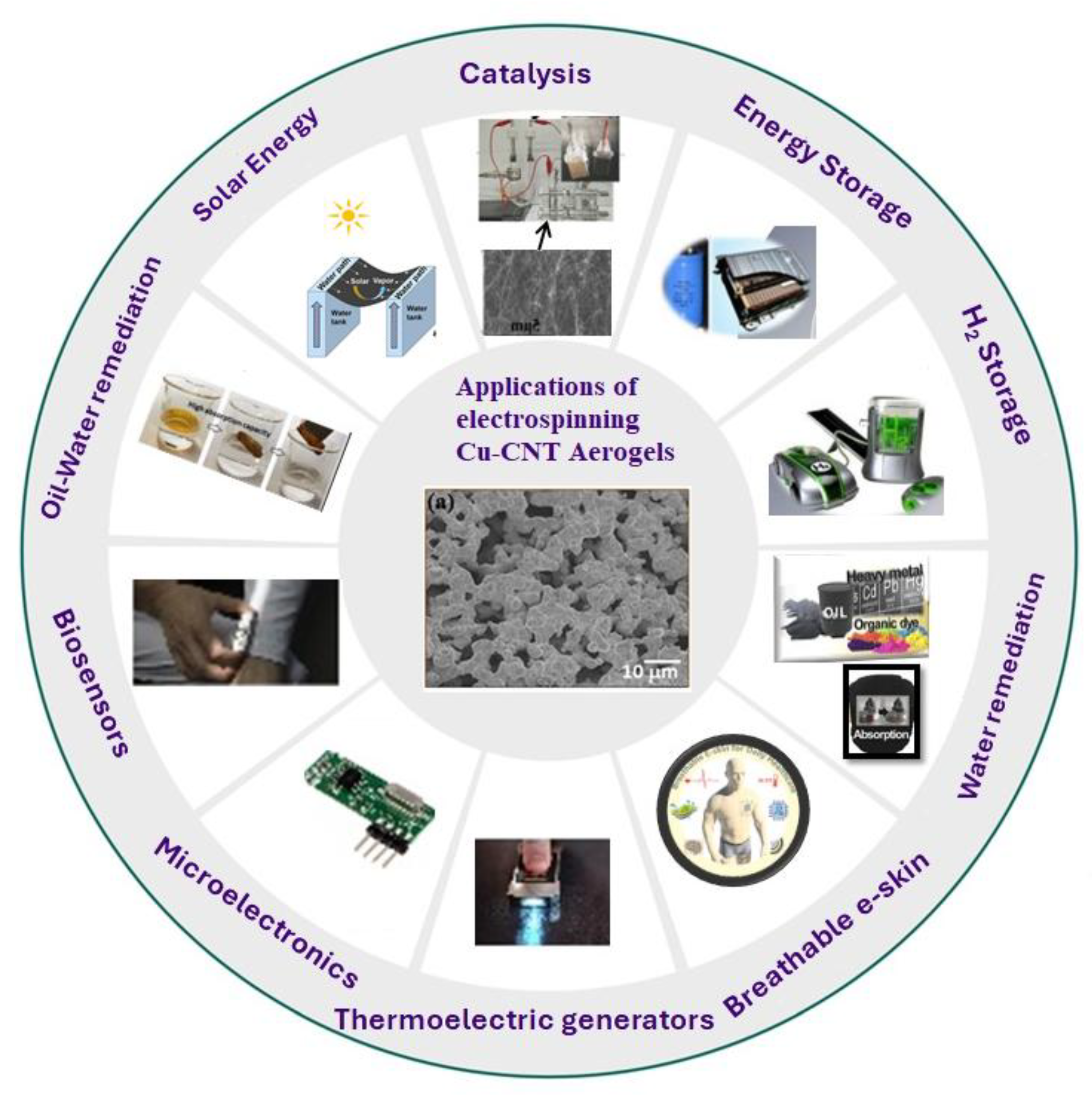
Potential Applications of Cu-CNT as Aerogels
Electrospun Cu-CNT nanofiber-based aerogels hold significant potential for a wide array of applications spanning diverse fields. These applications encompass biosensors, supercapacitors, batteries, solar cells, hydrogen energy storage, breathable electronic skin[45], catalysis [46] , thermoelectric generators, microelectronics, and more. As previously mentioned, the unique properties of electrospun Cu-CNT aerogels include high porosity, low density, and a hierarchy of open pores.
In the context of energy storage, the suitability of these aerogels as efficient electrode materials is evident. Key requisites for effective electrode materials encompass high chemical and mechanical stability to ensure a prolonged cycle life, superior electrical conductivity to facilitate rapid electron transfer, hierarchical open pores to facilitate swift mass transfer, and a substantial specific surface area to accommodate a greater number of reaction sites. Figure 8 illustrates the extensive range of commercial applications that Cu-CNT aerogels can serve. On a microscopic scale, these aerogels consist of delicate networks of clustered nanoparticles, often endowed with unique attributes such as remarkable strength-to-weight and surface-area-to-volume ratios.
Historically, the majority of aerogels have been constructed using silica (for applications like radiation detectors and thermal insulation) or pyrolyzed organic polymers (for battery electrodes and supercapacitors), serving as ultralightweight structural media. The novel contribution of this research lies in the fabrication of Cu-CNT aerogels through electrospinning, introducing a novel class of aerogels based on carbon nanotubes (CNTs). The utilization of electrospinning for Cu-CNT aerogel fabrication enables precise manipulation of network properties. This versatility allows for fine-tuning CNT concentrations, optimizing CNT dispersion processes, reinforcing networks with materials like polyvinylpyrrolidone (PVP), and infusing or backfilling them with polymeric fluids. Through this approach, we are empowered to explore an array of possibilities and applications for these remarkable materials.
Moreover, these Cu-CNT aerogels have demonstrated real-time practical applicability, as they can be easily soldered into functional circuits. This attribute underscores the promising potential of electrospun Cu-CNT aerogels as lightweight and versatile materials, heralding a novel approach in various domains. The strength of this innovative system lies in its distinctiveness, offering scalability to industrial levels and presenting opportunities for numerous other applications.The versatility of electrospun Cu-CNT aerogels opens doors to a wide range of possibilities. These materials hold promise in applications such as field-effect transistors, single-electron transistors, microelectronics, semiconductors, conducting composites, supercapacitors, batteries, nano electronics, doping, magnetic nanotubes, and hydrogen storage. The ability to apply these aerogels across such a diverse spectrum of fields underscores their potential impact and the far-reaching opportunities they present.
Conclusions
In summary, our study has led to the development of a high-performance electrically conductive Cu-CNT aerogel with remarkable properties. The achieved electrical conductivity is approximately 0.5x10³ S/cm, accompanied by a low density of 1.669 g/c.c. Additionally, the estimated surface area is on the order of ~442 m²/g. The comprehensive confirmation studies conducted through SEM, XRD, XPS, FTIR, and Raman spectral analyses have unequivocally validated the presence of both copper and CNTs within the Cu-CNT aerogel system. These findings pave the way for a multitude of potential commercial applications for Cu-CNT aerogels. Notably, their unique combination of properties positions them as promising candidates for catalytic applications, sensors, and various types of storage devices. The substantial evidence presented in this study underscores the potential and versatility of Cu-CNT aerogels, rendering them a valuable addition to the realm of advanced materials with broad-ranging practical implications.
Author Contributions
Conceptualization, methodology, experimental validation, data collection, formal data analysis, by M.S.; and data analysis, writing-original draft preparation, writing review editing, validation by V.J.B.; Supervision, project administration, funding acquisition S.R. All authors have read and agreed to the final version of the manuscript.
Funding
This research received no external funding.
Data Availability Statement
Not applicable.
Acknowledgments
MS and VJB thank Seeram Ramakrishna.
Conflicts of Interest
The authors declare no conflict of interest.
References
- L.W. Hrubesh: J Non Cryst Solids, 1998, vol. 225, pp. 335–42.
- R.W. Pekala: J Mater Sci, 1989, vol. 24, pp. 3221–7.
- R.W. Pekala, J.C. R.W. Pekala, J.C. Farmer, C.T. Alviso, T.D. Tran, S.T. Mayer, J.M. Miller, and B. Dunn: J Non Cryst Solids, 1998, vol. 225, pp. 74–80.
- S. Cao, N. S. Cao, N. Yao, and K.L. Yeung: J Solgel Sci Technol, 2008, vol. 46, pp. 323–33.
- H. Luo, G. H. Luo, G. Churu, E.F. Fabrizio, J. Schnobrich, A. Hobbs, A. Dass, S. Mulik, Y. Zhang, B.P. Grady, A. Capecelatro, C. Sotiriou-Leventis, H. Lu, and N. Leventis: J Solgel Sci Technol, 2008, vol. 48, pp. 113–34.
- M.S. Bono, A.M. M.S. Bono, A.M. Anderson, and M.K. Carroll: J Solgel Sci Technol, 2010, vol. 53, pp. 216–26.
- J. Liao, P. J. Liao, P. Liu, Y. Xie, and Y. Zhang: Science of The Total Environment, 2021, vol. 768, p. 144212.
- Benad, F. Jürries, B. Vetter, B. Klemmed, R. Hübner, C. Leyens, and A. Eychmüller: Chemistry of Materials, 2018, vol. 30, pp. 145–52.
- J.L. Mohanan and S.L. Brock: J Solgel Sci Technol, 2006, vol. 40, pp. 341–50.
- P. Brown and L.J. Hope-Weeks: J Solgel Sci Technol, 2009, vol. 51, pp. 238–43.
- M.B. Bryning, D.E. M.B. Bryning, D.E. Milkie, M.F. Islam, L.A. Hough, J.M. Kikkawa, and A.G. Yodh: Advanced Materials, 2007, vol. 19, pp. 661–4.
- J. Kong, E. J. Kong, E. Yenilmez, T.W. Tombler, W. Kim, H. Dai, R.B. Laughlin, L. Liu, C.S. Jayanthi, and S.Y. Wu: Phys Rev Lett, 2001, vol. 87, p. 106801.
- L.A. Hough, M.F. L.A. Hough, M.F. Islam, P.A. Janmey, and A.G. Yodh: Phys Rev Lett, 2004, vol. 93, p. 168102.
- B. Vigolo, C. B. Vigolo, C. Coulon, M. Maugey, C. Zakri, and P. Poulin: Science (1979), 2005, vol. 309, pp. 920–3.
- M.B. Bryning, M.F. M.B. Bryning, M.F. Islam, J.M. Kikkawa, and A.G. Yodh: Advanced Materials, 2005, vol. 17, pp. 1186–91.
- S.S. KISTLER: Nature, 1931, vol. 127, pp. 741–741.
- T.F. Baumann, G.A. T.F. Baumann, G.A. Fox, J.H. Satcher, N. Yoshizawa, R. Fu, and M.S. Dresselhaus: Langmuir, 2002, vol. 18, pp. 7073–6.
- J. Zou, J. J. Zou, J. Liu, A.S. Karakoti, A. Kumar, D. Joung, Q. Li, S.I. Khondaker, S. Seal, and L. Zhai: ACS Nano, 2010, vol. 4, pp. 7293–302.
- Q. Zhou, B. Q. Zhou, B. Jin, J. Chen, Y. Xiao, S. Chu, and R. Appl Organomet Chem. [CrossRef]
- S.M. Zhang, S.L. S.M. Zhang, S.L. Jin, M.L. Jin, X. Shao, and R. Zhang: Adv Mat Res, 2014, vol. 1061–1062, pp. 112–9.
- X. Xiao, Y. X. Xiao, Y. Xu, X. Lv, J. Xie, J. Liu, and C. Yu: J Colloid Interface Sci, 2019, vol. 545, pp. 1–7.
- K. Li, M. K. Li, M. McGuire, A. Lupini, L. Skolrood, F. List, B. Ozpineci, S. Ozcan, and T. Aytug: ACS Appl Nano Mater, 2020, vol. 3, pp. 6863–75.
- Fest, F. Tristán, W. Perez-Vigueras, G.J. Labrada-Delgado, D. Meneses-Rodríguez, and S.M. Vega-Díaz: Carbon Trends, 2023, vol. 10, p. 100235.
- Karan, N.S. Sharma, M. Darder, Y. Su, S.M. Andrabi, S.M.S. Shahriar, J. V. John, Z. Luo, M.A. DeCoster, Y.S. Zhang, and J. Xie: ACS Omega, 2024, vol. 9, pp. 9765–81.
- X. Lu, P. X. Lu, P. Lin, Y. Huang, X. He, C. Yi, J. Sun, M.U. Farid, A.K. An, and J. Advanced Fiber Materials. [CrossRef]
- Zhang, Z. Qu, C. Ruiz-Agudo, L. Yang, B. Chi, Y. Kong, and F. Wang: Carbon N Y, 2025, vol. 234, p. 120020.
- V.J. Babu, R.P. V.J. Babu, R.P. Rao, A.S. Nair, and S. J Appl Phys. [CrossRef]
- M. Sireesha, V. M. Sireesha, V. Jagadeesh Babu, and S. Ramakrishna: RSC Adv, 2015, vol. 5, pp. 103308–14.
- V.J. Babu, D.V.B. V.J. Babu, D.V.B. Murthy, V. Subramanian, V.R.K. Murthy, T.S. Natarajan, and S. J Appl Phys. [CrossRef]
- V. Jagadeesh babu, S. V. Jagadeesh babu, S. Vempati, Y. Ertas, and T. Uyar: RSC Adv, 2015, vol. 5, pp. 66367–75.
- Y. Fu, L. Y. Fu, L. Zhang, and G. Chen: Carbon N Y, 2012, vol. 50, pp. 2563–70.
- L. Martin, H. L. Martin, H. Martinez, D. Poinot, B. Pecquenard, and F. Le Cras: The Journal of Physical Chemistry C, 2013, vol. 117, pp. 4421–30.
- T. Boningari, D.K. T. Boningari, D.K. Pappas, P.R. Ettireddy, A. Kotrba, and P.G. Smirniotis: Ind Eng Chem Res, 2015, vol. 54, pp. 2261–73.
- S. Hamamda, A. S. Hamamda, A. Jari, S. Revo, K. Ivanenko, Y. Jari, and T. Avramenko: Nanoscale Res Lett, 2017, vol. 12, p. 251.
- K. Chu, C. K. Chu, C. Jia, and W. Li: Applied Physics A, 2013, vol. 110, pp. 269–73.
- Firkowska, A. Boden, A.-M. Vogt, and S. Reich: J Mater Chem, 2011, vol. 21, p. 17541.
- K. Chu, C. K. Chu, C. Jia, W. Li, and P. Wang: physica status solidi (a), 2013, vol. 210, pp. 594–9.
- M. Ciszewski, D. M. Ciszewski, D. Janas, and K.K. Koziol: Batteries, 2019, vol. 5, p. 60.
- Maqbool, F.A. Khalid, M.A. Hussain, and N. Bakhsh: IOP Conf Ser Mater Sci Eng, 2014, vol. 60, p. 012040.
- C.L.P. Pavithra, B. V. C.L.P. Pavithra, B. V. Sarada, K. V. Rajulapati, T.N. Rao, and G. Sundararajan: Sci Rep, 2014, vol. 4, p. 4049.
- N.F. Khusnun, A.A. N.F. Khusnun, A.A. Jalil, S. Triwahyono, N.W.C. Jusoh, A. Johari, and K. Kidam: Physical Chemistry Chemical Physics, 2016, vol. 18, pp. 12323–31.
- M.B. Bazbouz, A. M.B. Bazbouz, A. Aziz, D. Copic, M. De Volder, and M.E. Adv Electron Mater. [CrossRef]
- A.A. Sahraei, H.N. A.A. Sahraei, H.N. Saeed, A. Fathi, M. Baniassadi, S.S. Afrookhteh, and M.K. Besharati Givi: Science and Engineering of Composite Materials, 2017, vol. 24, pp. 345–52.
- Subramaniam, T. Yamada, K. Kobashi, A. Sekiguchi, D.N. Futaba, M. Yumura, and K. Hata: Nat Commun, 2013, vol. 4, p. 2202.
- V.J. Babu, M. V.J. Babu, M. Anusha, M. Sireesha, S. Sundarrajan, S.S.A. Abdul Haroon Rashid, A.S. Kumar, and S. Ramakrishna: Polymers (Basel), 2022, vol. 14, p. 2219.
- V. Jagadeesh Babu, S.S.A. V. Jagadeesh Babu, S.S.A. Abdul Haroon Rashid, S. Sundarrajan, and S. Ramakrishna: Sustainable Chemistry, 2023, vol. 4, pp. 26–37.
Figure 1.
Evolution of Electrospun Cu-CNT conductive aerogels and related Aerogels/CNT Milestones starting from 1931 after the invention of Kistler in 1931[Ref [16,17,18,19,20,21,22,23,24,25,26]].
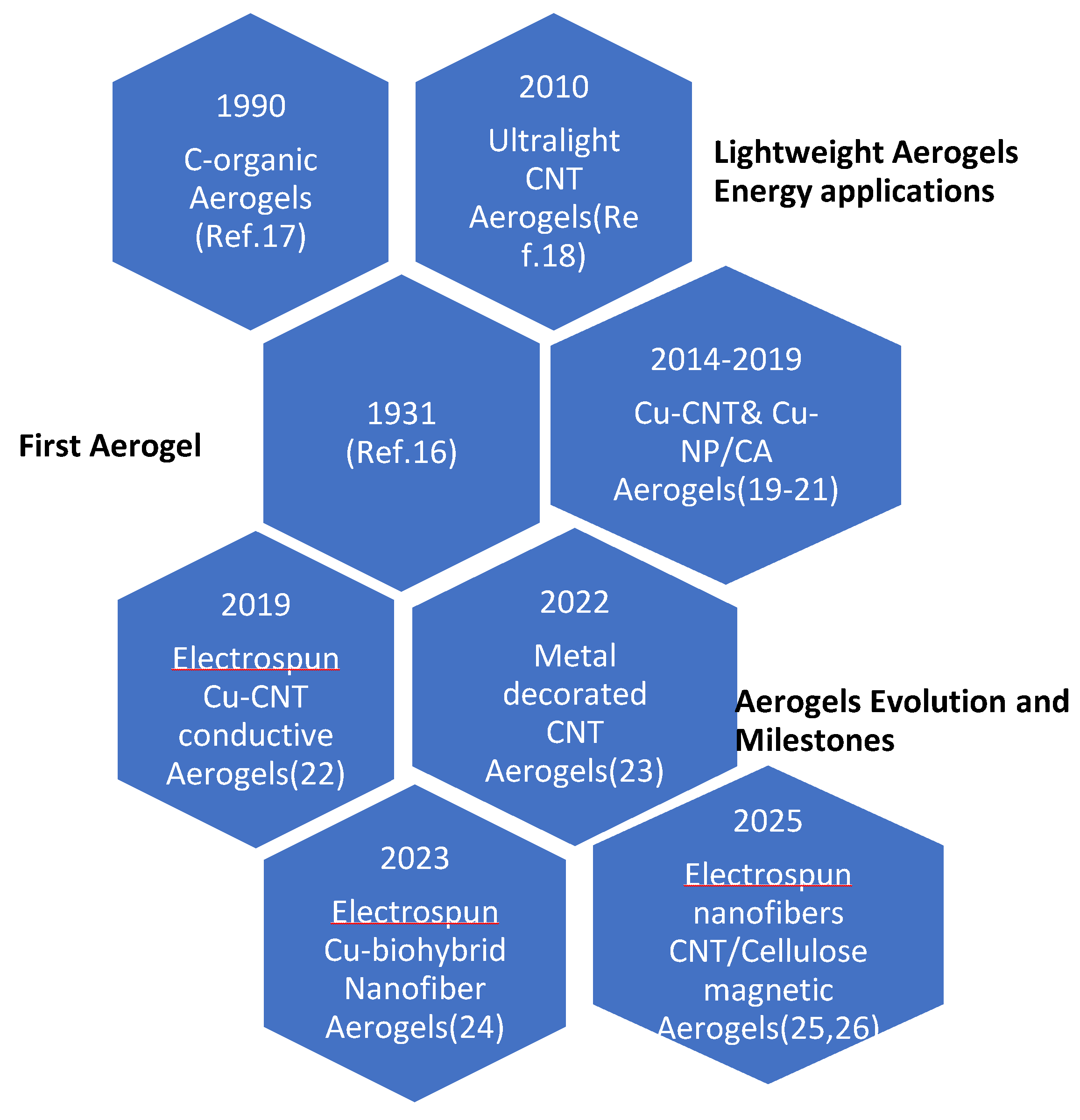
Figure 2.
SEM images of electrospun (a) Cu-CNTs different location showing interconnected network (b) Cu-CNT at higher magnifications showing connectivity (c) CNTs are clearly seen at magnification x50,000 and (d) EDS showing only pure Copper is present.
Figure 2.
SEM images of electrospun (a) Cu-CNTs different location showing interconnected network (b) Cu-CNT at higher magnifications showing connectivity (c) CNTs are clearly seen at magnification x50,000 and (d) EDS showing only pure Copper is present.
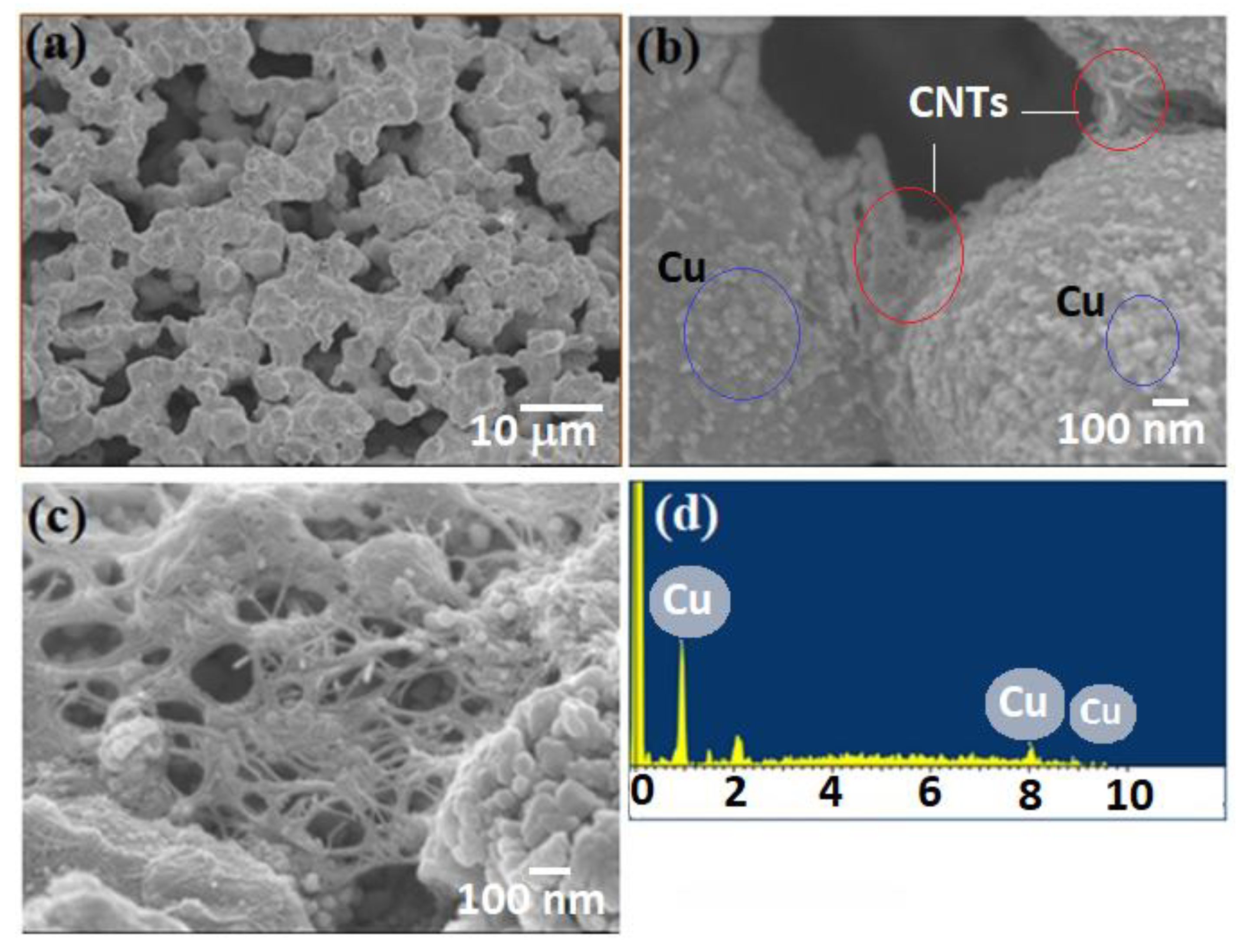
Figure 3.
XRD showing (a) Cu and CNTs present in the Cu-CNTs system. The inset peak C (002) comes from the CNTs especially (b) by fitting peak Cu (200) the surface area is estimated about ~442 m2/g, the table infers that the peak fitting values centred at 43.376 of 2θ.
Figure 3.
XRD showing (a) Cu and CNTs present in the Cu-CNTs system. The inset peak C (002) comes from the CNTs especially (b) by fitting peak Cu (200) the surface area is estimated about ~442 m2/g, the table infers that the peak fitting values centred at 43.376 of 2θ.
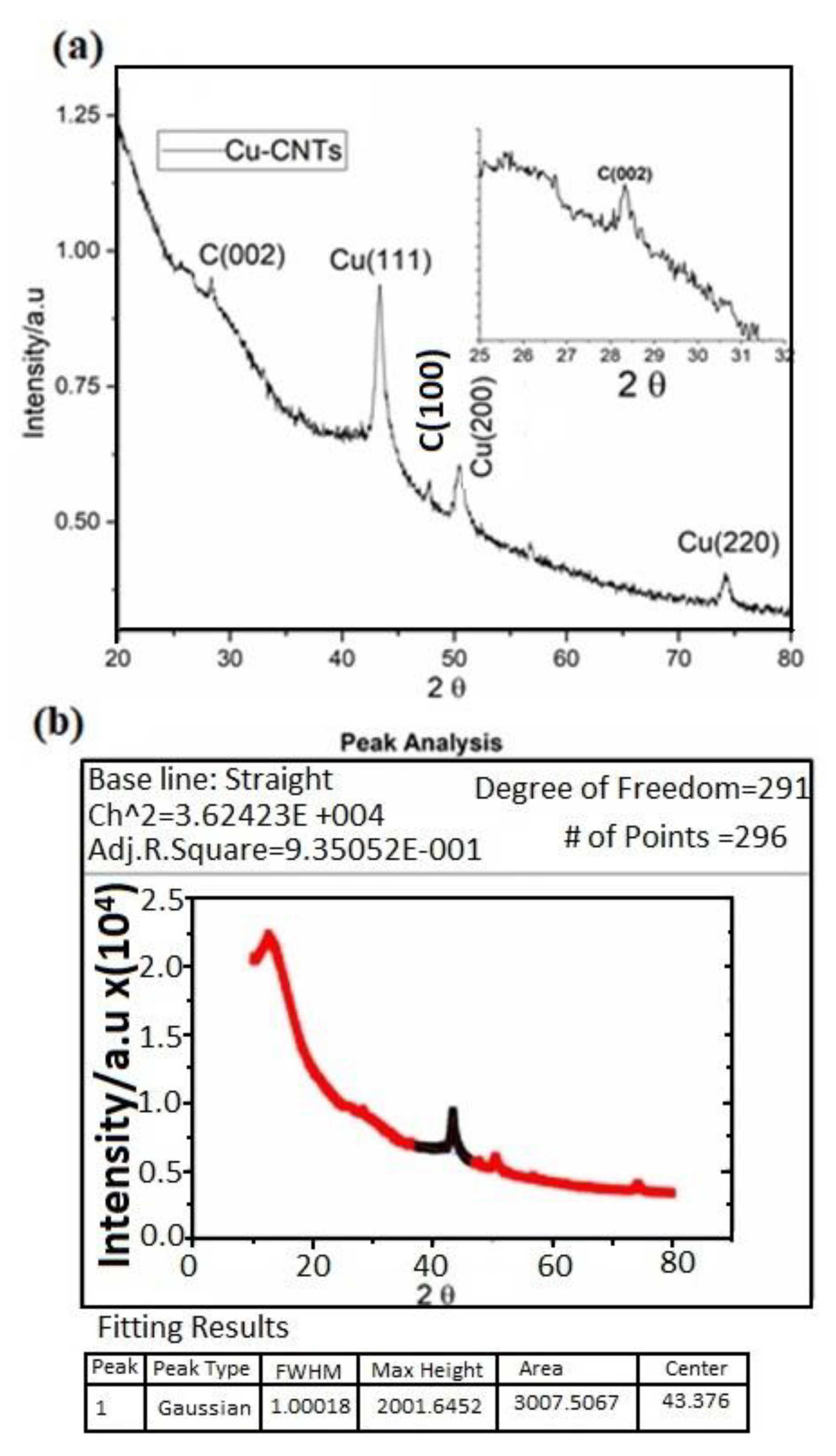
Figure 4.
(a) XPS survey spectra for the Cu-CNT wire and (b) XPS Cu2p for Cu-CNTs wire shows about seven peaks including three satellite peaks.
Figure 4.
(a) XPS survey spectra for the Cu-CNT wire and (b) XPS Cu2p for Cu-CNTs wire shows about seven peaks including three satellite peaks.
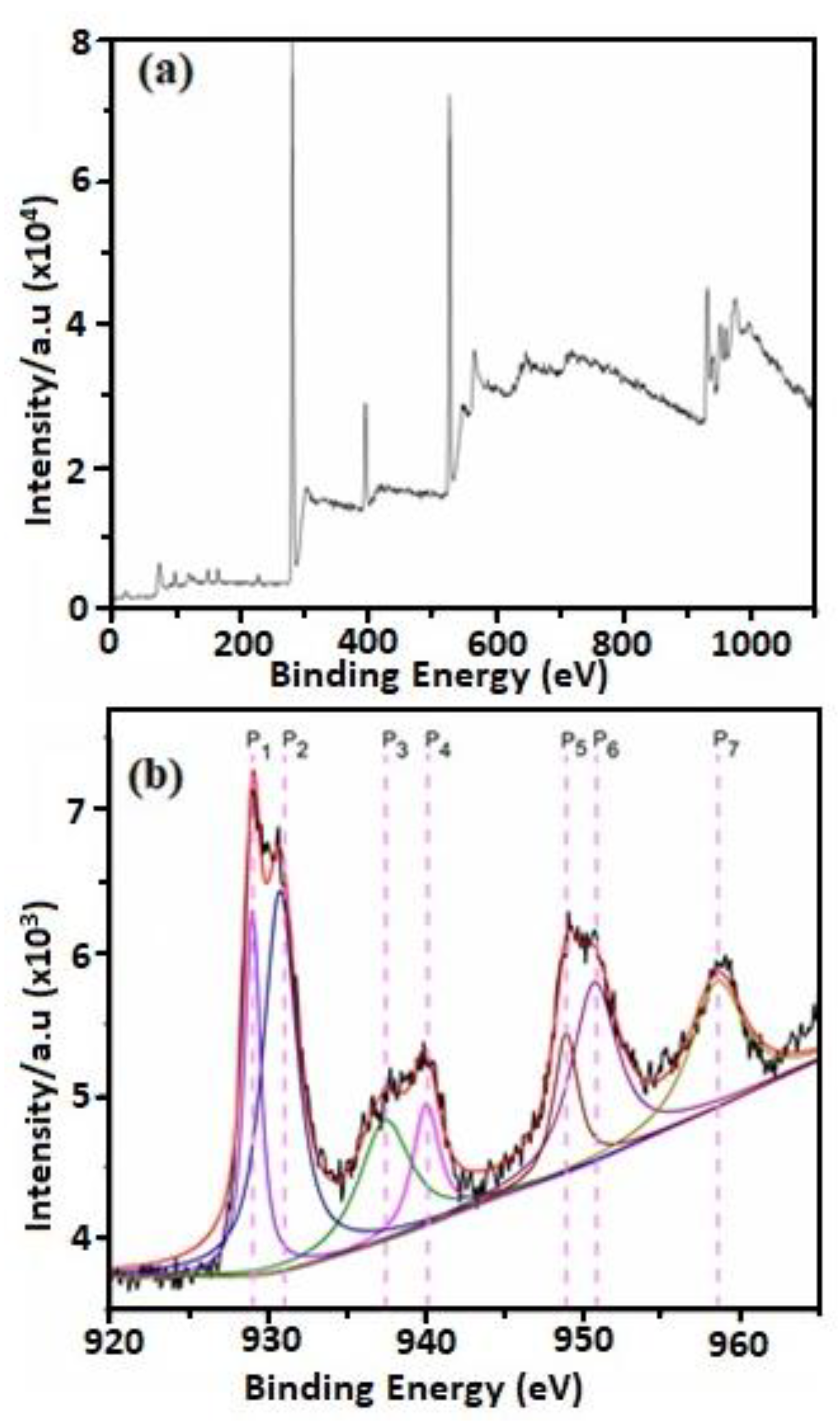
Figure 5.
(a) Auger Spectra from XPS identification of pure metallic copper and (b) O1s peak from XPS.
Figure 5.
(a) Auger Spectra from XPS identification of pure metallic copper and (b) O1s peak from XPS.
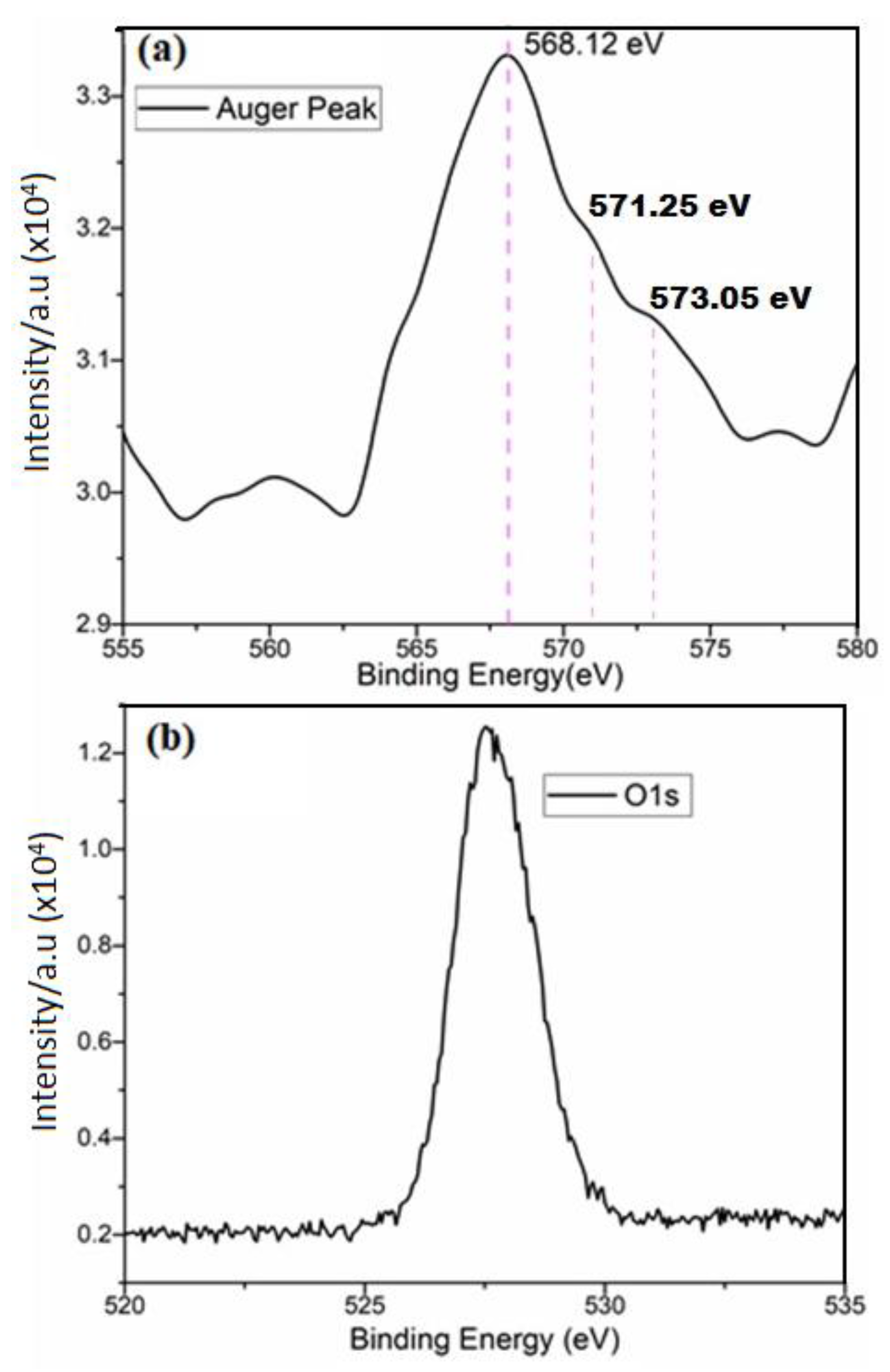
Figure 6.
(a)FTIR spectra showing Cu and CNTs presence and (b) Raman spectroscopy for the Cu-CNT aerogel.
Figure 6.
(a)FTIR spectra showing Cu and CNTs presence and (b) Raman spectroscopy for the Cu-CNT aerogel.
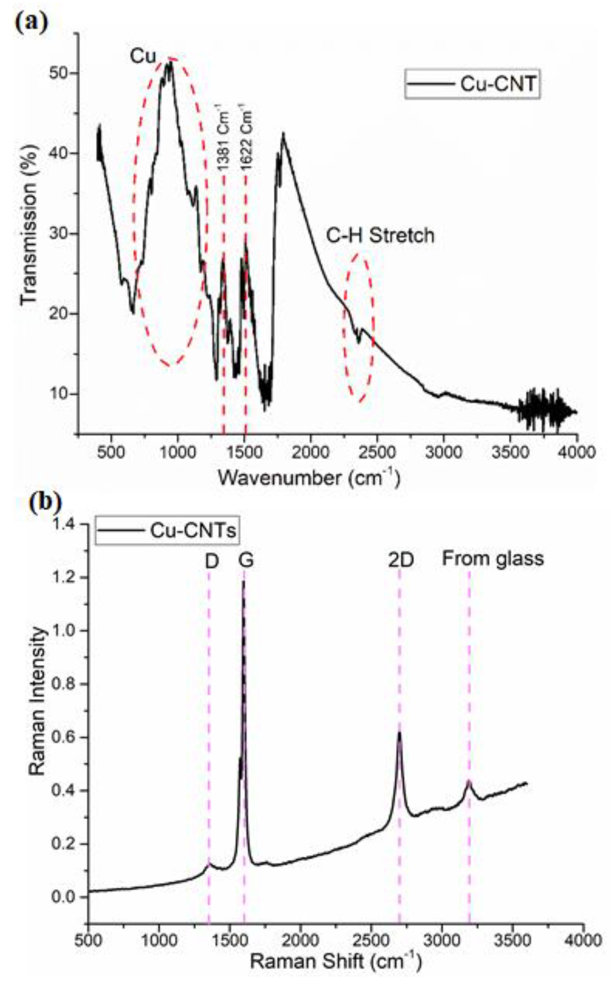
Figure 7.
Electrical measurements using four probes on electrospun Cu-CNT aerogels.
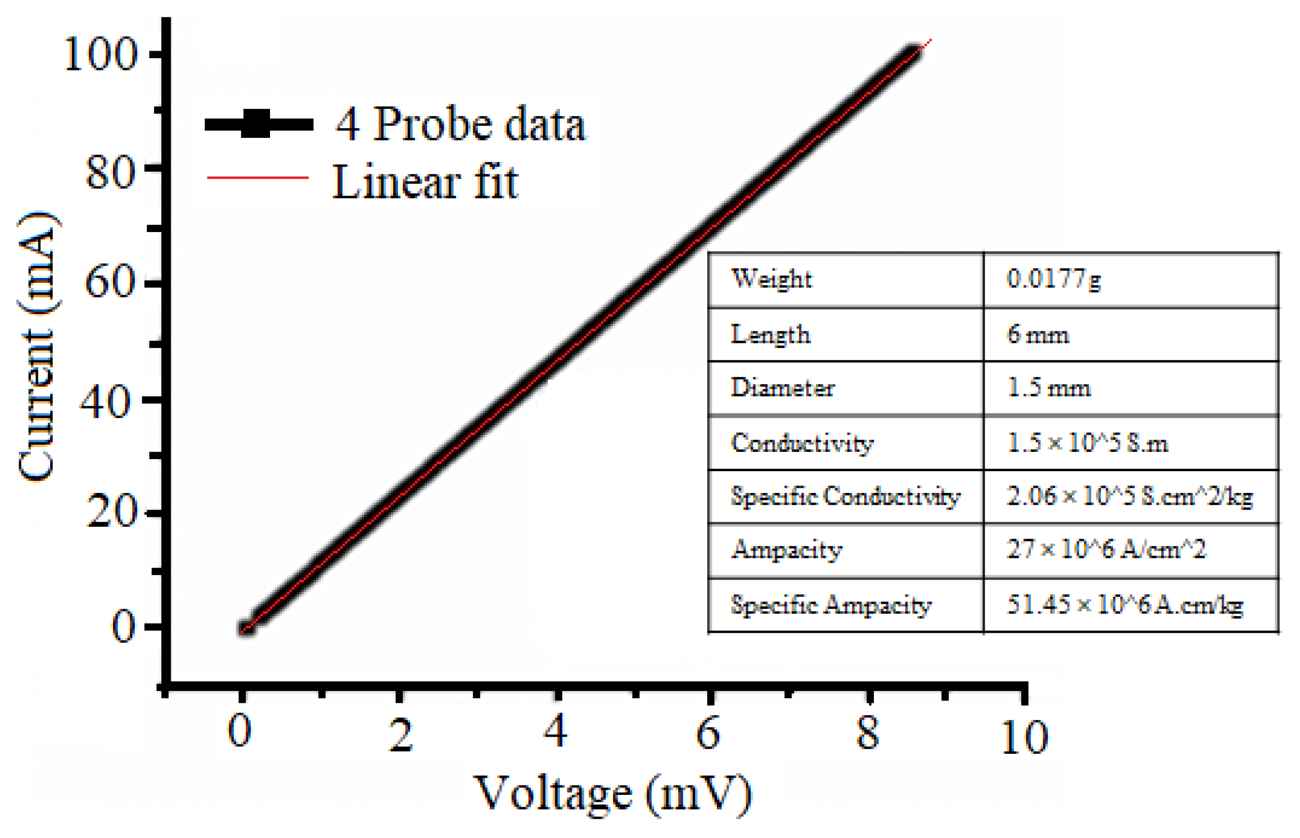
Figure 8.
Cu-CNT aerogels showing commercial/research oriented applications.
Disclaimer/Publisher’s Note: The statements, opinions and data contained in all publications are solely those of the individual author(s) and contributor(s) and not of MDPI and/or the editor(s). MDPI and/or the editor(s) disclaim responsibility for any injury to people or property resulting from any ideas, methods, instructions or products referred to in the content. |
© 2025 by the authors. Licensee MDPI, Basel, Switzerland. This article is an open access article distributed under the terms and conditions of the Creative Commons Attribution (CC BY) license (http://creativecommons.org/licenses/by/4.0/).
Copyright: This open access article is published under a Creative Commons CC BY 4.0 license, which permit the free download, distribution, and reuse, provided that the author and preprint are cited in any reuse.


