Submitted:
03 September 2025
Posted:
04 September 2025
You are already at the latest version
Abstract
Roll-to-roll production of thin organic and large-area electronic (TOLAE) devices often involves a 2-step process per functional layer: an un-pattered continuous deposition of the film and subsequent structuring process by for instance laser ablation. Thin film organic devices should be protected using ultra-barrier films. To perform laser ablation of functional layers on top of such barrier films, in particular that of transparent electrodes, an unprecedented selectivity of laser ablation is required to completely remove the layers without damaging the thin-film barrier layers underneath. When performing highly-selective laser ablation of indium tin oxide (ITO) on top of silicon nitride (SiN) barrier layers, we observed the emergence of visible large-scale patterns due to local variations in ablation quality. Our investigations using a very sensitive Raman spectroscopy setup show that the ablation variations originate from minute optical path length differences present in the heat-stabilized plastic substrates and locally consequential destructive or constructive interference occurs between the reflected light from the back of the substrate and incoming laser beam. By performing laser ablation under an angle such that the reflected and incoming laser beam do not spatially overlap, highly-selective uniform laser ablation can be performed, even for two transparent overlapping layers.
Keywords:
laser ablation
; roll-to-roll
; large-area processing
; photovoltaics
; thin-film electronics
1. Introduction
Polyethylene terephthalate (PET) is the preferred substrate in thin organic and large-area electronic (TOLAE) devices due to the combination of its optical transparency and low price [1,2]. For applications such as organic light emitting diodes (OLEDs) and organic- or perovskite photovoltaics (OPVs or PSC) the deposition and annealing temperatures during processing require the use of heat-stabilized (bi-axially stretched) PET (150 °C). When process temperatures up to 220 °C are required, heat-stabilized PEN can be used [3]. Since TOLAE devices are typically extremely sensitive to degradation by the ambient, the devices have to be encapsulated with a thin film barrier stack from both top and bottom side, since the water vapor transmission rate (WVTR) of the substrate itself is at least 6 orders of magnitude too high to protect the device with a sufficient life time [4]. From a cost and practical point of view, an unstructured roll-to-roll (R2R) deposition of each layer is preferred, directly on top of a barrier film. After completion of the device, a second barrier foil can be laminated on top and, thereby, limiting the stack to contain 2 plastic films. Compared to the more conventional 3-film approach, where a separate PET or PEN substrate is used as base for device fabrication and after which the whole stack is sealed with 2 separate barrier films, the fabrication directly on the barrier film leads to a significant cost reduction and in fact a better performance, since PET/PEN substrates by themselves contain small amounts of residual water that will degrade the device over time. For the realization of R2R thin film electronics, the individual layers have to be structured separately with a stand-alone process, such as laser ablation.
Over the last decades, laser patterning of indium tin oxide (ITO) on glass and PET substrates [5,6,7,8] has been investigated intensively for photovoltaics (PV) and display applications [9,10,11,12,13,14]. Here, the main requirement is the complete removal of the transparent conductive (TC) material in the laser track and (partial) damage to the substrate underneath is largely inconsequential. Fewer studies have investigated laser ablation of functional layers deposited directly on top of barrier films [15,16,17]. Direct laser structuring of layers on top of thin-film barriers is much more challenging as selective removal of the layers is required while barrier properties are to be maintained, i.e., no damage should occur to the thin-film barrier underneath. In particular, when a transparent layer has to be structured on top of a transparent barrier layer and no clear wavelength-selective ablation can be performed, careful tuning of the laser ablation process parameters are required, possibly in combination with tuning of the optical properties of the layers. For example, Naithani et al. reported that selective laser ablation can be achieved by changing the optical properties of the barrier film [18].
In a previous study, we already reported on the investigations of direct laser structuring of TC layers, the so-called P1 scribe, deposited on top of R2R produced barrier films for its use as bottom electrode in R2R PV applications [19]. In that report, the process window for laser structuring of the TC layer was performed in such a way that a) no damage is introduced to the barrier film and b) full electrical isolation in the TC layer is achieved. During these process investigations, irregular ablation of the TC layer was observed. In this report we investigate the origin of the irregular ablation quality.
Here, we used the same stack as previously reported [19] with the most commonly used transparent electrode material, indium tin oxide (ITO) deposited on top of a state-of-the-art R2R produced barrier film, consisting of a heat-stabilized PET substrate with an organic planarization layer (OCP, organic coating for planarization) and a single hydrogenated amorphous silicon nitride (SiN) barrier layer; i.e. PET/OCP/SiN. The barrier films have been extensively quantified using the optical Ca-test [20] and show an overall WVTR < 10-6 g.m-2.day-1, which is determined by the intrinsic properties of the SiN due to the extremely low pinhole density present, i.e. ~ 0.03 pinholes/cm2 (determined from 1250 cm2 barrier film per individual barrier test). Logically, any damage induced by laser ablation, resulting in pinholes or cracks in the SiN, will have detrimental effects on overall barrier performance, resulting in fast degradation of the device processed on top.
During the laser ablation process investigations, irregular ablation of the ITO was observed. These irregularities are best described as local changes in the ablation diameter and ablation depth within a single laser track. The pattern of irregularities seems to result from a large-scale effect originating in the samples since it spans multiple laser tracks over a large area and is independent of the ablation direction. The variations along the laser tracks have a significant effect as they lead to either unwanted local barrier damage by over-ablation or insufficient isolation due to non-removed TC layer by under-ablation. Furthermore, the variations in ablation quality hamper the precise determination of a process window for highly-selective laser ablation.
Comparable laser ablation studies do not show these strong variations along the laser track, which is likely due to the fact that all have been performed with the layers directly on top of plastic substrates or glass [6,21,22,23] and damage underneath the ablation track is non-critical. In literature, laser induced damage or patterns [24,25,26,27,28,29] are either ripples on the surface with a period distance which is similar to the laser wavelength range or patterns induced by the biaxial stretching of the PET, so-called naps and walls [30]. The periodicity of these wall structures is in the range of 1 µm up to 8 µm. The patterns we observed have a periodicity at a much larger scale, in the range of 1 mm up to 1 cm. Here, we focus on the long-range laser inconsistencies that appear during the TC laser ablation and provide solutions for uniform highly-selective ablation on top of plastic substrates and barrier foils.
2. Materials and Methods
The substrate used for laser ablation was a R2R produced barrier film (WVTR < 10-6 g.m-2.day-1) with ITO as transparent conductor. The barrier film consist of a heat stabilized PET of 125 µm thickness, an organic coating for planarization (OCP) of 22.3 µm thickness and a low-temperature hydrogenated silicon nitride (SiN) inorganic barrier layer of 150 nm thickness; PET/OCP/SiN. Samples from the roll-to-roll barrier film were cut out and a 135nm thick ITO layer is deposited on the barrier film by sputtering.
A 1064 nm picosecond laser (Talisker Ultra, Coherent) was used to laser structure ITO (P1 scribe) and stop on the SiN layer. A square area of 3x3 cm was fully covered with laser scribes of 3 cm in length, with a spacing of 100 µm. To look in detail at the optical properties of the barrier films and the emerged interference patterns upon ITO ablation, Raman spectroscopy was used.
A Raman spectroscopy setup was used with a laser with 633 nm wavelength exciting the sample through an optical microscope objective. The lateral resolution and depth specificity is determined by the choice of microscope objective. The light coming back from the sample, of which the majority will be reflected laser light, is passing a filter which eliminates all light with a wavelength ≤ 633 nm. All wavelengths longer than 633 nm are detected by the system and analyzed with dedicated software.
The accompanying software can analyze the spectrum with a mathematical method by splitting up the detected spectrum in several components (so called principal components, PCs) that build up the total spectrum. Each of these components can represent a physical property of the sample. The PCs are orthogonal functions that contain the most variance in the original spectrum. The equation of the PCs can be written as follows [31];
where is the original Raman spectroscopy data, ,…… are the orthogonal principle components of the original data and ,,…… are the coordinate values or scores that project the original Raman spectroscopy on the new orthogonal principle components. When an area of a sample is scanned by Raman, the changes in each of the principal components can be plotted in a mapping by giving a colour difference for the amount of change in component. Hence, for each element or property of the spectrum (physical or mathematical) a mapping can be made of the strength or variation of that component over the sample area and we can see if the large-scale pattern that we like to analyse appears as an optical effect in the detected signal.
3. Results and Discussion
The in-house developed methodology to obtain selective ablation settings for a specific laser in combination with a specific TC layer was previously described in detail [19] and an overview for the currently used combination of a 1064 nm picosecond laser and ITO is provided in the Supporting Information. The optimized laser settings using a 1064 nm picosecond laser for ablation of ITO on SiN barrier films, were at a fluence level of 635 mJ/cm2 at 47 % pulse overlap (ablation speed 200 mm/s). When ablating at these settings an irregular ablation was observed along the laser track with locally over- and under ablation, where the SiN suffers from damage or the ITO has not been completely removed, respectively. The variable ablation behavior manifests as local changes in the ablation diameter and ablation depth within a single laser track, see Figure 1B. The pattern of irregularities seems to result from a large-scale effect originating in the samples since it spans multiple laser tracks resulting in a large pattern, see Figure 1A. A first assumption was that the pattern might originate due to thickness variations in the OCP coating on top of PET. The investigations by white light interferometry, see Supporting Information, clearly showed that the height variations in the samples and associated in- and out of focus of the laser spot, are not the cause for the irregular ablation quality.
To investigate in detail the optical properties of the substrates, the laser structured samples were investigated by Raman spectroscopy. To compare a laser patterned area with the non-patterned area adjacent to it (see Figure 2A), a large area mapping by Raman was carried out over the sample. Principal component analysis was applied to the obtained Raman spectrum. Figure 2C shows the Raman spectrum detected from a single point (blue line). The majority of the spectrum is caused by a small fluorescence originating in the sample and the peak close to 3100 cm-1 is a Raman peak originating from the PET substrate. The spectral shape of the principal component PC3(λ), shown by the black line in Figure 2C, represents the interference for the small amount of fluorescence present in the Raman spectrum. The stitched optical microscopy image obtained by the Raman setup is shown in Figure 2A. Here, the stitched areas (repetitive dark areas) and the emerging fringe-pattern due to the laser scribing can be clearly identified. In Figure 2B the same mapping is shown, but in this case each pixel has a colour defined by the variation observed in PC3(λ) score. Albeit that the score mapping appears to be distorted in the laser scribed area due to the presence of laser tracks and associated rougher surface area, from the stitched optical microscopy image and the PC3(λ) score mapping it can be observed that the emerging pattern present in the laser scribed area continues in the adjacent un-patterned area when looking at the score mapping of PC3(λ), which is a component related to the interference in measured fluorescence.
To understand the nature of the PC3(λ) score value, the Raman spectrum was plotted for the maximum and minimum PC3(λ) score location, shown in Figure 3 and the actual locations on the sample are depicted by the blue and red dots in the previous Figure 2B. In Figure 3 only a part of the spectrum is plotted for the range 2650 – 2950 cm-1 (corresponding to 760.6 – 778.3 nm). Besides the small difference in absolute value of the Raman spectrum at both locations, it can be observed that the interference pattern in fluorescence is present at both locations but has shifted with respect to each other. When we fit the derivative (to remove absolute value differences) of the interference pattern with a sine function, we obtain a wavelength of 20.01 +/- 0.02 cm-1 and 20.00 +/- 0.02 cm-1 for the highest and lowest PC3(λ) score location, respectively. These wavelengths are identical within the error of measurement and, thereby, unrelated to the PC3(λ) score. In fact, for the maximum and minimum location in the mapping, the shift of interference is exactly equal to half the wavelength (10 cm-1) of the interference pattern, implying that the PC3(λ) score gives a value for phase shift of the interference pattern in the fluorescence spectrum. More details are provided in Figure S5 and S6 in the Supporting Information .
The optical path length of a stack of layers is determined by a summation of the product of the refractive index (n) and thickness (d) of the individual layers:
From the number of fringes (k) present between 2 chosen wavelengths (λ1 and λ2) in an interference spectrum, the OPL can be determined by the Swanepoel method [32], where:
For the range chosen in Figure 3 between 2650 – 2950 cm-1 (corresponding to λ 1 = 760.6 nm and λ2 = 778.3 nm) there are exactly 15 fringes (k), resulting in an OPL = 250.0 µm for the fluorescence. The difference in optical path length (ΔOPL) to induce the shift in the interference spectrum can be calculated by the relative shift in wavelength of the spectrum between a peak and valley. The wavelength for the interference spectrum equals 20 cm-1, corresponding to 1.18 nm. Hence, the difference between peak and valley is 0.59 nm and for the wavelength of 770 nm (2810.8 cm-1) this equals to a ΔOPL= 192 nm only, or a variation of 0.08 % in optical path length.
To determine where these variations in optical path length originate from, we also investigated bare PET substrates that were used in the fabrication of the barrier films. The Raman spectrum is provided in Figure S7 together with a spectrum of the full barrier stack with ITO. A similar large-area pattern in the PC3(λ) score mapping was obtained. As can be seen in Figure S7, the interference pattern has a slightly different periodicity due to the significant different optical path length. The wavelength for the fluorescence interference spectrum was 22.83 cm-1 (1.36 nm). By the Swanepoel method we find an optical path length for bare PET of OPLPET = 216.7 µm from the interference spectrum. When subtracting the OPLPET from that obtained on the full stack (OPL), the thickness of the OCP can be deduced using Equation 1. Using a measured refractive index of 1.50 for OCP, we obtain an OCP layer thickness of 21.9 µm, very close to the measured average value of 22.3 ± 0.1 µm (average of 72 measurements from 6 separate barrier films) and even more so when we take into account that the substrate is assumed to be exactly 125 µm in thickness based on the information provided by the supplier. The results clearly indicate that the origin of optical path length variations is present in the PET substrate.
The minute variations of 0.08% in optical path length present within the PET substrates can be the result of thickness variations (corresponding to 100 nm variations for a film of 125 µm in thickness), refractive index variations (corresponding to 0.001 variations for a refractive index of 1.58), or due to a combination of both parameters. We have determined the optical path length variation between the highest score value and lowest score value of the PC3(λ) score mapping, which coincidentally happen to be continuously connected from a low to high value in the mapping in Figure 2B. However, moving from the point with highest score value (blue dot, Figure 2B) upwards, another low value ring is observed. Since the interference pattern can shift with multiple wavelengths, we cannot exclude that larger variations in the optical path length exist within the PET substrate, resulting in local minima and maxima in PC3(λ) score mapping.
To understand how these small variations in the optical path length in the PET can influence the laser ablation uniformity, it is crucial to realize that the majority of the laser light is passing through the transparent layers and some of that light reflects from the rear of the substrate. The reflected light from the rear of the substrate can interfere with the incoming laser light of the same laser pulse (laser pulse duration is approximately 15 ps and duration for light to travel twice through the stack is about 1.5 ps). Logically, the locations where we observed maxima and minima in PC3(λ) score from fluorescence at approximately 770 nm, will not be the same maxima and minima locations for the 1064 nm laser light source used for ablation due to the longer wavelength of the light. Furthermore, the OPL (250.0 µm) that was determined from the interference spectrum is not identical to that of the light travelled through the stack, which can be determined using Equation 1 and resulting in 231.48 µm. Using these two wavelengths of 770 nm and 1064 nm and associated optical path lengths, we can model the phase shift of the light using a sine function provided in Equation S1 in the Supporting Information (see also Figure S6), which in case of 1064 nm resulted in constructive and destructive interference and associated variations in ablation quality. The obtained optical periodicity is represented in Figure 4A, where the sine function for 770 and 1064 nm is plotted as a function of potential thickness variations or refractive index variations in the 125 µm PET substrate. Clearly, a different periodicity is present between the observed fluorescence interference around 770 nm and that expected for 1064 nm laser ablation, where the periodicity for 1064 nm is approximately 1.4 times larger. This also implies that the large area pattern observed by PC3(λ) score mapping and that obtained by laser ablation are likely not identical. We verified this by combining the optical microscopy image of the 1064 nm laser patterned side of the sample in Figure 2A with that of the ~770 nm interference shift (PC3(λ) score) mapping at the un-patterned side in Figure 2B. The combined image is provided in Figure 4B. At the interface between the two images we can see that this is indeed the case; at some locations a dark area in the optical microscopy image (corresponding to more damage by ablation) lines up with low values in the PC3(λ) score mapping and at other locations with a high value. In short, as expected, the periodicity in the large area pattern is different for both cases and the periodicity of the pattern emerging from laser ablation being larger compared to that seen in the PC3(λ) score mapping. Albeit slightly different in periodicity, both patterns originate from the same variations in optical path length in the PET substrate.
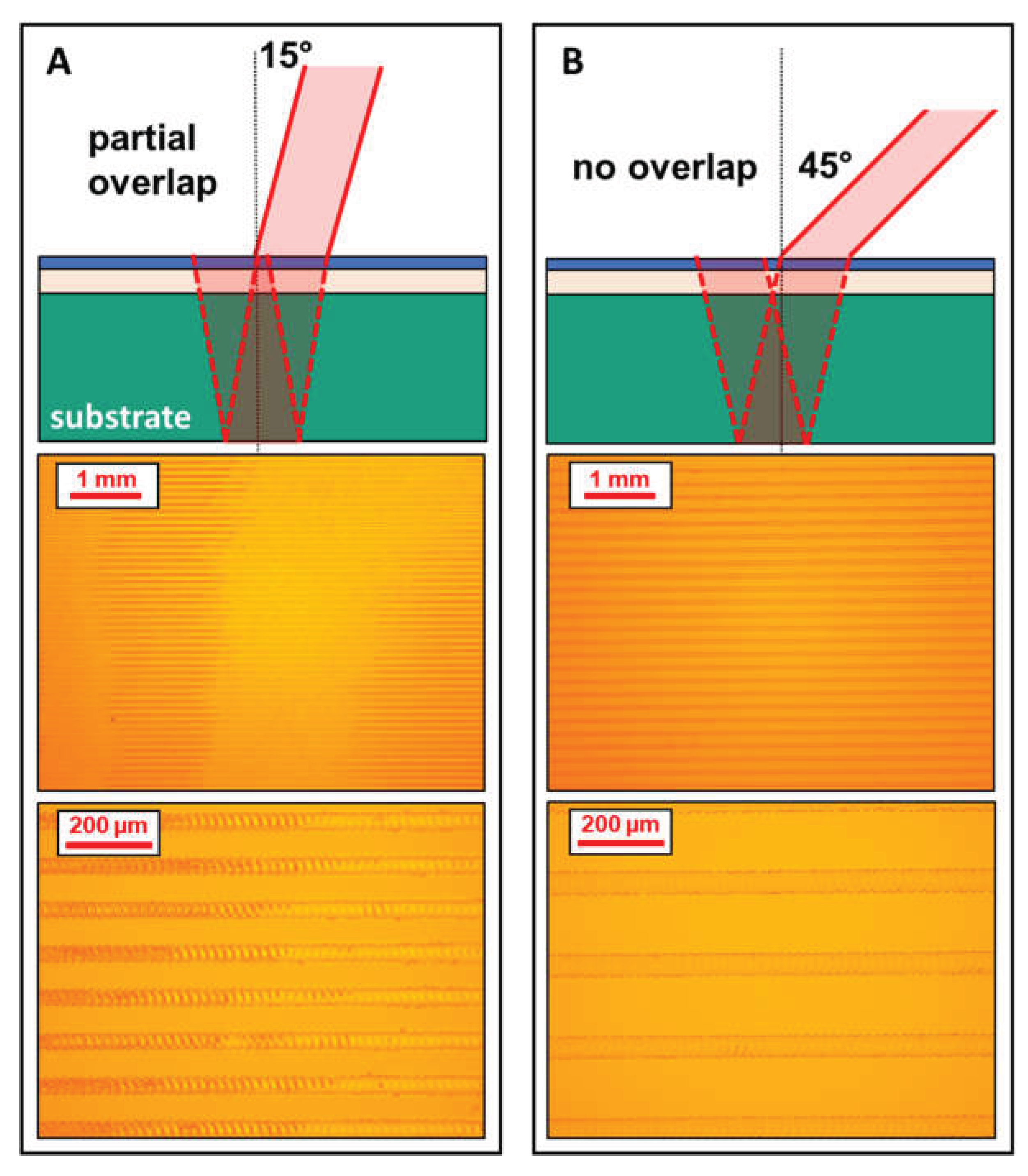
When the theory of constructive and destructive interference between incoming laser light and reflected laser light from the rear of the substrate is correct, we can try to minimize or eliminate this effect. For example, incorporating a near-infrared absorbing sacrificial layer underneath the transparent electrode could result in an optically selective ablation of the sacrificial layer together with the TC layer on top. The drawbacks for such a solution are the increased cost by increased complexity of the stack and limiting transparency in the near-infrared range for the PV application. Another possible solution could be to ensure that the light reflected from the back of the substrate is not overlapping with the incoming laser light. When this would be attempted with a scattering layer or higher substrate roughness, it would limit the transparency and possible solar cell performance, as well as the appearance of the PV product. We propose and performed a more basic solution that could be readily applied in the roll-to-roll production of PV; by performing laser ablation under an angle such that the reflected light from the back is not overlapping with the incoming laser spot. Using a 50 µm spot diameter of the laser and the thickness and refractive index of the individual layers, we can calculate the overlap at the substrate surface between incoming and reflected light. Below a 16° off-normal angle the spots overlap at the surface and above 16° no overlap is present. The results are shown in Figure 5, where laser ablation was performed under an off-normal angle of 15°, with a partial overlap between the reflected light and incoming light, and at a 45° angle where no overlap is present. As can be seen from the optical microscopy images, the laser ablation at 15° off-normal still results in fluctuations in ablation diameter and depth, but less severe compared to the previous perpendicular ablation. At 45° the laser ablation is completely uniform over the full track and reproducible over larger areas with multiple tracks. These results not only confirm the constructive-destructive interference concept due to optical path length variations in the PET substrate, but also provide a solution that can be directly implemented for the laser patterning of roll-to-roll produced thin film stacks, without the additional need of changing the stack.
4. Conclusions
Laser ablation of ITO on R2R produced barrier films showed non-uniform ITO ablation with varying ablation depth and diameter along a single ablation track, resulting in electrically non-isolated locations of the ITO or locations with compromised barrier functionality. Over larger areas the fluctuations in ablation quality resulted in a large scale pattern. We used the very sensitive optical technique of Raman spectroscopy, in combination with principal component analysis and mapping, to investigate the origin of these ablation quality fluctuations. By looking at the shift of interference pattern from the small fluorescence present in the Raman spectrum and the comparison to bare PET films, we concluded that origin for ablation variations was due to minute variations (as small as 0.08 %) in optical path length present in bi-axially stretched plastic substrates. Constructive and destructive interference between the incoming laser light and that reflected by the rear of the substrate occurs depending on the local optical path length, resulting in differences in ablation quality. A straightforward solution was provided by performing laser ablation under an angle, such that the reflected laser light does not spatially overlap with the incoming laser pulse. Performing laser ablation under an angle, in combination with the methodology developed for optimization of the laser ablation process, a highly selective laser ablation of (transparent) thin films can be performed without damaging the thin transparent barrier layers underneath.
Acknowledgements
Part of this work has received funding from the European Com-mission, Horizon 2020 Research and Innovation Action, in the framework of the ALABO project, Grant agreement No 644026.
References
- J. Willmann, D. Stocker, E. Dörsam, Characteristics and evaluation criteria of substrate-based manufacturing. Is roll-to-roll the best solution for printed electronics?, Org. Electron. (2014). [CrossRef]
- M. Kaltenbrunner, M.S. White, E.D. Głowacki, T. Sekitani, T. Someya, N.S. Sariciftci, S. Bauer, Ultrathin and lightweight organic solar cells with high flexibility, Nat. Commun. (2012). [CrossRef]
- W.A. MacDonald, M.K. Looney, D. MacKerron, R. Eveson, R. Adam, K. Hashimoto, K. Rakos, Latest advances in substrates for flexible electronics, J. Soc. Inf. Disp. (2007). [CrossRef]
- J. Lewis, Material challenge for flexible organic devices, Mater. Today. (2006). [CrossRef]
- D. Ashkenasi, A. Rosenfeld, Processing multilayer systems using femtosecond, picosecond, and nanosecond laser pulses at different wavelengths, in: Phot. Process. Microelectron. Photonics, 2002. [CrossRef]
- S. Xiao, S.A. Fernandes, A. Ostendorf, Selective patterning of ITO on flexible PET Substrate by 1064nm picosecond Laser, in: Phys. Procedia, 2011. [CrossRef]
- G. Račiukaitis, M. Brikas, M. Gedvilas, T. Rakickas, Patterning of indium-tin oxide on glass with picosecond lasers, Appl. Surf. Sci. (2007). [CrossRef]
- Risch, R. Hellmann, Picosecond laser patterning of ITO thin films, in: Phys. Procedia, 2011. [CrossRef]
- M. Park, B.H. Chon, H.S. Kim, S.C. Jeoung, D. Kim, J.I. Lee, H.Y. Chu, H.R. Kim, Ultrafast laser ablation of indium tin oxide thin films for organic light-emitting diode application, Opt. Lasers Eng. (2006). [CrossRef]
- M. Henry, P.M. Harrison, J. Wendland, Laser direct write of active thin-films on glass for industrial flat panel display manufacture, J. Laser Micro Nanoeng. (2007). [CrossRef]
- C. Moorhouse, D. Karnakis, C. Kapnopoulos, A. Laskarakis, E. Mekeridis, S. Logothetidis, Laser patterning of smart nanomaterials for reel-to-reel production of organic photovoltaic (OPV) devices, J. Laser Micro Nanoeng. (2015). [CrossRef]
- S.F. Tseng, W.T. Hsiao, K.C. Huang, D. Chiang, M.F. Chen, C.P. Chou, Laser scribing of indium tin oxide (ITO) thin films deposited on various substrates for touch panels, Appl. Surf. Sci. (2010). [CrossRef]
- R.S. Patel, D. Clark, J. Bovatsek, Laser scribing: A key enabling technology for manufacturing of low cost thin film photovoltaic cells, in: 26th Int. Congr. Appl. Lasers Electro-Optics, ICALEO 2007 - Congr. Proc., 2007. [CrossRef]
- Y. Shin, B. Jeon, S. Shin, S. Lim, J. Souk, T. Odajima, 49.1 : Fabrication of 23” PVA LCD Panel by Laser Ablation Process of ITO, SID Symp. Dig. Tech. Pap. 40 (2009) 727. [CrossRef]
- D. Karnakis, A. Kearsley, M. Knowles, Ultrafast laser patterning of OLEDs on flexible substrate for solid-state lighting, J. Laser Micro Nanoeng. (2009). [CrossRef]
- D. Karnakis, T. Stephens, G. Chabrol, Maskless selective laser patterning of PEDOT:PSS on barrier/foil for organic electronics applications, in: Laser Appl. Microelectron. Optoelectron. Manuf. XVIII, 2013. [CrossRef]
- R. Mandamparambil, H. Fledderus, G. Van Steenberge, A. Dietzel, Patterning of Flexible Organic Light Emitting Diode (FOLED) stack using an ultrafast laser, Opt. Express. (2010). [CrossRef]
- S. Naithani, R. Mandamparambil, H. Fledderus, D. Schaubroeck, G. Van Steenberge, Fabrication of a laser patterned flexible organic light-emitting diode on an optimized multilayered barrier, Appl. Opt. (2014). [CrossRef]
- H. Fledderus, H.B. Akkerman, A. Salem, N. Friedrich Schilling, U. Klotzbach, Patterning of organic photovoltaic on R2R processed thin film barriers using IR laser sources, in: Laser-Based Micro- Nanoprocessing XI, 2017. [CrossRef]
- G. Nisato, H. Klumbies, J. Fahlteich, L. Müller-Meskamp, P. Van De Weijer, P. Bouten, C. Boeffel, D. Leunberger, W. Graehlert, S. Edge, S. Cros, P. Brewer, E. Kucukpinar, J. De Girolamo, P. Srinivasan, Experimental comparison of high-performance water vapor permeation measurement methods, Org. Electron. (2014). [CrossRef]
- M.F. Chen, Y.P. Chen, W.T. Hsiao, Z.P. Gu, Laser direct write patterning technique of indium tin oxide film, Thin Solid Films. (2007). [CrossRef]
- Schoonderbeek, V. Schütz, O. Haupt, U. Stute, Laser processing of thin films for photovoltaic applications, J. Laser Micro Nanoeng. (2010). [CrossRef]
- McDonnell, D. Milne, C. Prieto, H. Chan, D. Rostohar, G.M. O’Connor, Laser patterning of very thin indium tin oxide thin films on PET substrates, Appl. Surf. Sci. (2015). [CrossRef]
- M. Birnbaum, Modulation of the reflectivity of semiconductors, J. Appl. Phys. (1965). [CrossRef]
- M. Siegrist, G. Kaech, F.K. Kneubühl, Formation of a periodic wave structure on the dry surface of a solid by TEA-CO2-laser pulses, Appl. Phys. (1973). [CrossRef]
- H.M. Van Driel, J.E. Sipe, J.F. Young, Laser-induced periodic surface structure on solids: A universal phenomenon, Phys. Rev. Lett. (1982). [CrossRef]
- J.E. Sipe, J.F. Young, J.S. Preston, H.M. Van Driel, Laser-induced periodic surface structure. I. Theory, Phys. Rev. B. (1983). [CrossRef]
- J.F. Young, J.S. Preston, H.M. Van Driel, J.E. Sipe, Laser-induced periodic surface structure. II. Experiments on Ge, Si, Al, and brass, Phys. Rev. B. (1983). [CrossRef]
- J.F. Young, J.E. Sipe, H.M. Van Driel, Laser-induced periodic surface structure. III. Fluence regimes, the role of feedback, and details of the induced topography in germanium, Phys. Rev. B. (1984). [CrossRef]
- F.R. WAGNER, Scanning excimer laser ablation of poly(ethylene terephthalate) (PET) and its application to rapid prototyping of channels for microfluidics, 2264 (2000).
- X. Li, T. Yang, S. Li, D. Wang, Y. Song, S. Zhang, Raman spectroscopy combined with principal component analysis and k nearest neighbour analysis for non-invasive detection of colon cancer, Laser Phys. (2016). [CrossRef]
- R. Swanepoel, Determination of the thickness and optical constants of amorphous silicon, J. Phys. E. (1983). [CrossRef]
Figure 1.
A photograph of a laser scribed area in ITO on barrier film (A), where a large area pattern emerges from local variations along the ablation tracks. An optical microscopy image from the individual laser tracks showing the variations in ablation diameter and depth (B).
Figure 1.
A photograph of a laser scribed area in ITO on barrier film (A), where a large area pattern emerges from local variations along the ablation tracks. An optical microscopy image from the individual laser tracks showing the variations in ablation diameter and depth (B).
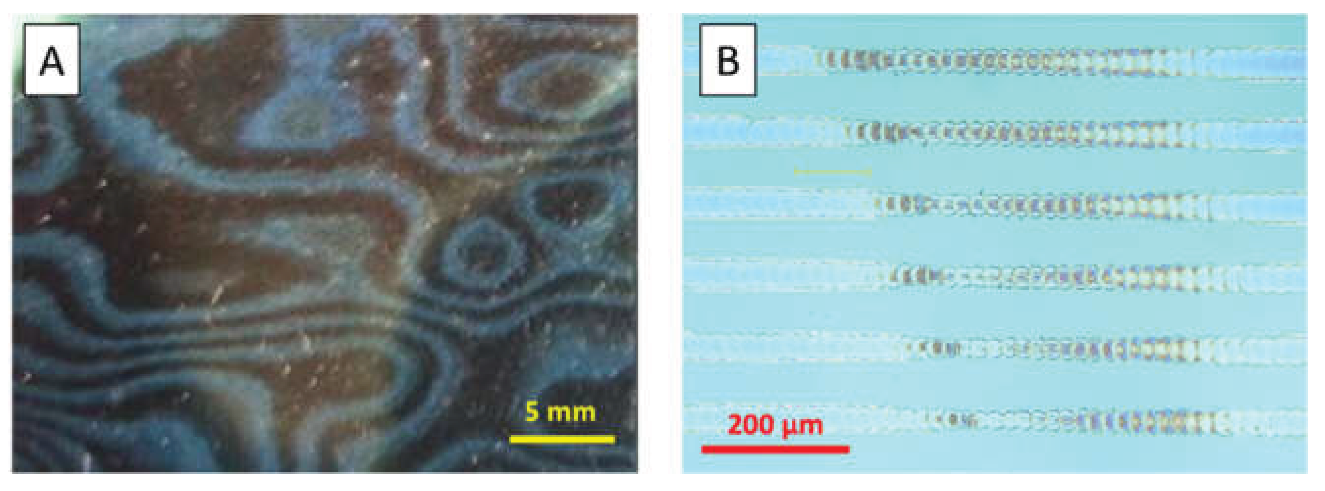
Figure 2.
A stitched image obtained by optical microscopy of the area used for the Raman spectroscopy, where at the left hand side laser tracks with variations are present, and the plain sample is present at the right hand side (A). A score mapping of the third principal component, PC3(λ) (B), where the red dot is the location with the minimum score for PC3(λ) in the mapped area, and the blue dot the maximum score location. An example of the spectrum detected from a single point in the Raman mapping (C). For each pixel a spectrum is recorded (blue line). This spectrum is mathematically split up in principal components. Here, principal component 3 is depicted by the black line, which is related to the interference in the fluorescence signal.
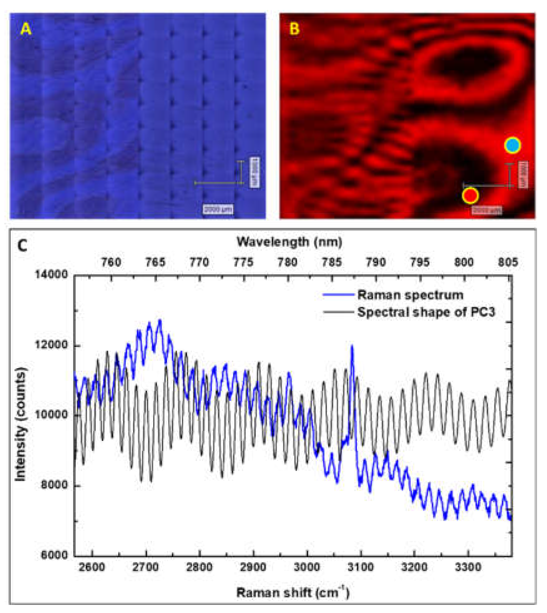
Figure 3.
Part of the Raman spectrum between 2650 – 2950 cm-1 (760.6 – 778.3 nm) at the location of the highest and lowest score, depicted by the blue and red dot in Figure 2B, where the shift in the interference by fluorescence is 10 cm-1, equal to half the wavelength of the interference spectrum.
Figure 3.
Part of the Raman spectrum between 2650 – 2950 cm-1 (760.6 – 778.3 nm) at the location of the highest and lowest score, depicted by the blue and red dot in Figure 2B, where the shift in the interference by fluorescence is 10 cm-1, equal to half the wavelength of the interference spectrum.
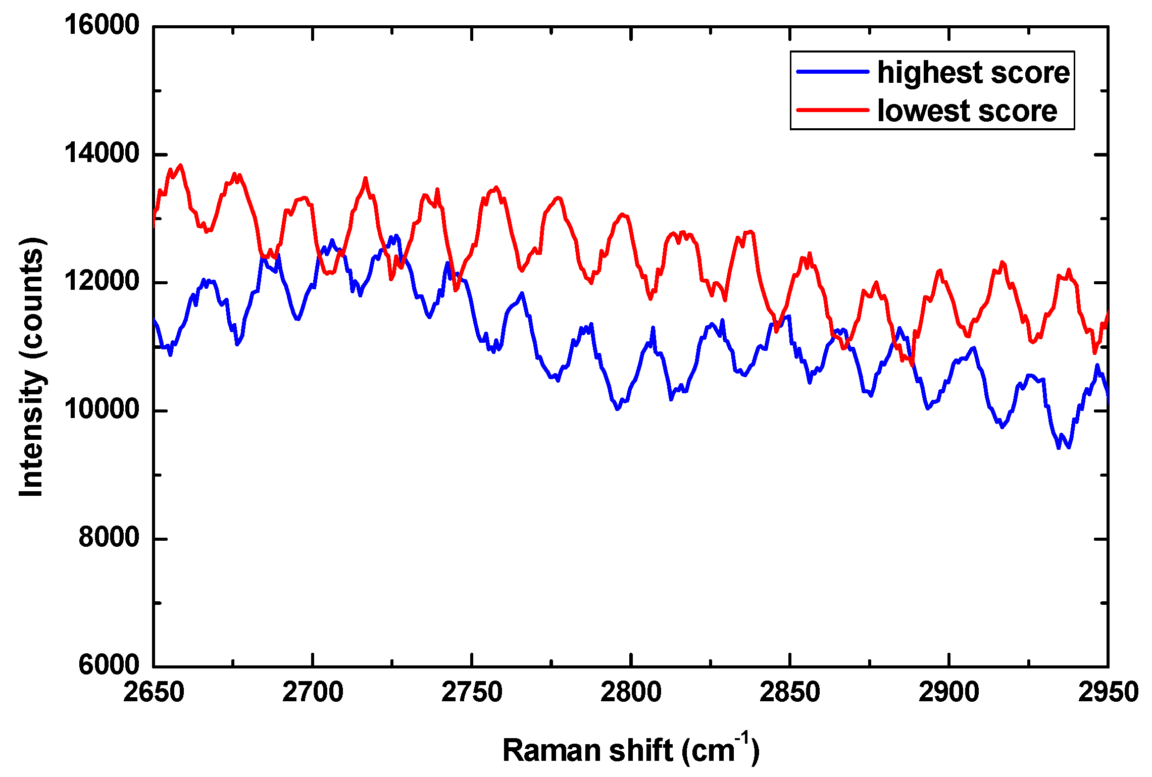
Figure 4.
Sine modulation representing the fluorescence interference spectral shift around 770 nm emission and the representation for 1064 nm laser light that is reflected from the rear of the substrate (A). For both graphs a different periodicity is obtained, which can also be observed when the optical microscopy image of the laser patterned area is compared to the PC3(λ) score mapping of the adjacent un-patterned area (B). At the interface of both images, the large area patterns do not perfectly line up with each other and show a different periodicity.
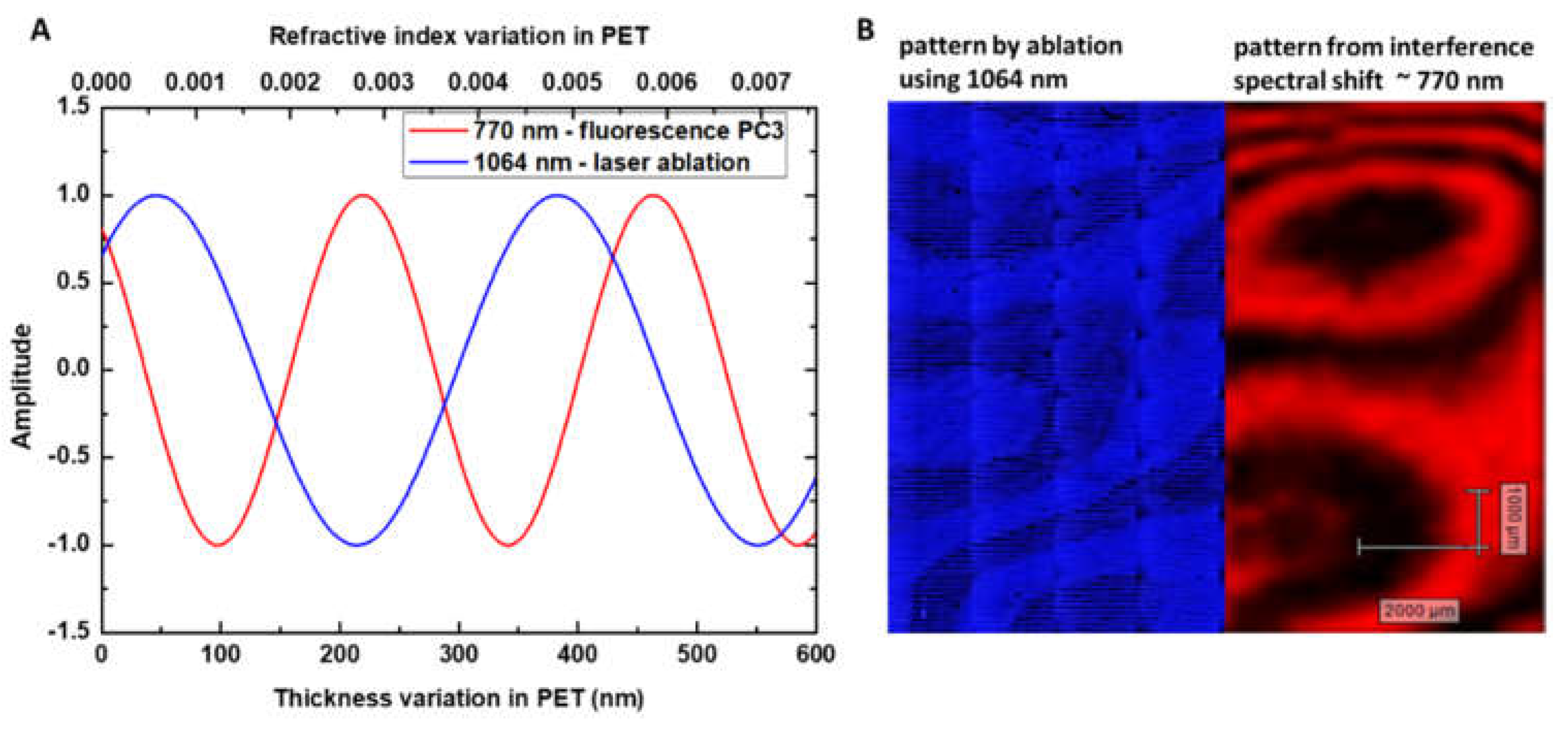
Figure 5.
An overview for the laser ablation under an angle for a 15 ° off-normal incident laser beam (A) and under a 45 ° off-normal angle (B). The optical microscopy images show that under a 15 ° angle for ablation, with partial overlap between incoming and reflected beam, still a large area fluctuation of ablation quality is observed, albeit with less variation compared to the previous perpendicular ablation. When overlap is avoided at an angle of 45 °, the ablation tracks are uniform and reproducible over larger area since no interference between incoming and reflected laser light occurs.
Disclaimer/Publisher’s Note: The statements, opinions and data contained in all publications are solely those of the individual author(s) and contributor(s) and not of MDPI and/or the editor(s). MDPI and/or the editor(s) disclaim responsibility for any injury to people or property resulting from any ideas, methods, instructions or products referred to in the content. |
© 2025 by the authors. Licensee MDPI, Basel, Switzerland. This article is an open access article distributed under the terms and conditions of the Creative Commons Attribution (CC BY) license (http://creativecommons.org/licenses/by/4.0/).
Copyright: This open access article is published under a Creative Commons CC BY 4.0 license, which permit the free download, distribution, and reuse, provided that the author and preprint are cited in any reuse.


