
Submitted:
23 October 2025
Posted:
23 October 2025
You are already at the latest version
Abstract
Addressing the urgent need for low-temperature processes in the manufacturing of flexible vehicle-mounted touch display devices, this study investigates the process-structure-performance relationships of indium tin oxide (ITO) thin films prepared by DC magnetron sputtering at temperatures far below the tolerance limit of transparent polyimide (CPI). By systematically adjusting the substrate temperature (30-300°C) combined with 230°C atmospheric annealing, a unique optimization effect was identified at the moderate deposition temperature of 110°C. Experimental results show that the sample deposited at 110°C followed by annealing exhibits optimal comprehensive performance: resistivity as low as 203 μΩ·cm, average visible light transmittance of 89.2%, surface roughness of 0.76 nm, and the ability to endure 100,000 bending cycles at a bending radius of R = 5 mm with a sheet resistance change rate of less than 10%. Microstructural analysis reveals that this process facilitates the complete conversion of Sn²⁺ to Sn⁴⁺ and the controlled formation of oxygen vacancies, leading to a synergistic improvement in carrier concentration (8.7×10²⁰ cm⁻³) and mobility (35.2 cm²/V·s). This work elucidates the crystallization kinetics and doping mechanisms of ITO thin films under low-temperature conditions, offering important theoretical foundations and technical pathways for the low-temperature fabrication of high-performance transparent electrodes in flexible vehicle-mounted touch display devices.
Keywords:
ITO thin films
; flexible vehicle-mounted touch display devices
; low-temperature process
; microstructure regulation
; optoelectronic properties
; transparent polyimide (CPI)
1. Introduction
With the rapid development of flexible electronics, the demand for high-performance flexible materials has significantly increased. Emerging application fields such as wearable health monitoring devices, flexible robotic skin, implantable medical electronics, and vehicle-mounted flexible touch displays [1,2,3,4] all require electronic components to adapt to various bending and folding deformations while maintaining excellent electrical performance and reliability such as impact resistance. This trend poses a fundamental challenge to traditional rigid electronic devices and has spurred research enthusiasm for flexible transparent conductive materials.
Among various transparent conductive materials, indium tin oxide (ITO) has long dominated the market due to its excellent optoelectronic properties (high conductivity, high visible light transmittance) and mature preparation processes [5]. However, its application in flexible devices still faces significant challenges. Firstly, the most commonly used flexible plastic substrates, such as polyethylene terephthalate (PET) and polyethylene naphthalate (PEN), have low glass transition temperatures (Tg) and cannot withstand the high deposition temperatures of traditional ITO sputtering processes and subsequent high-temperature annealing treatments [6]. ITO films prepared at low temperatures often suffer from poor crystalline quality and high defect density, resulting in electrical properties (such as resistivity) far inferior to those of films prepared on glass substrates [7,8]. Secondly, the significant coefficient of thermal expansion (CTE) mismatch between PET/PEN and ITO easily introduces substantial internal stress during device bending, leading to film cracking or even delamination from the substrate, severely limiting the device's mechanical reliability and service life [9].
Transparent polyimide (CPI) materials offer an ideal solution to the above bottlenecks. CPI not only possesses excellent mechanical properties, chemical stability, and high-temperature resistance (Tg > 350°C), but its thermal expansion coefficient can also be adjusted through molecular design to achieve better matching with ITO films. Although CPI itself has many advantages, to achieve compatibility with the entire flexible electronics manufacturing process chain (especially including heat-sensitive organic functional layers) and minimize thermal stress, developing processes for low-temperature preparation of high-performance ITO films remains a common goal pursued by both academia and industry [10,11].
Currently, although there have been studies on the low-temperature preparation of ITO films on CPI substrates, our team's previous research focused on improving the bending resistance of CPI-based ITO films [12], emphasizing structural optimization. This study conducts a systematic investigation of the synergistic effect of "deposition temperature - post-annealing treatment" and provides an in-depth explanation of its microscopic mechanism. In particular, the scientific question of how the deposition temperature affects the film's microscopic crystal structure, thereby determining the effectiveness of subsequent low-temperature annealing treatment, has not been clearly answered.
Based on this, this study innovatively proposes a "low-temperature deposition - post-annealing synergistic regulation" strategy, aiming to achieve the preparation of high-performance ITO films at temperatures far below the CPI tolerance limit. This paper systematically studies the regulation law of substrate temperature (30-300°C) during DC magnetron sputtering on the microstructure and chemical state of ITO films, and combined with 230°C atmospheric annealing treatment, analyzes in detail its impact on the final optoelectronic properties (resistivity, transmittance) and surface morphology of the films. Through characterization methods such as XRD, AFM, and XPS, it deeply reveals the conversion of Sn²⁺ to Sn⁴⁺, oxygen vacancy formation, and crystallization kinetics under low-temperature conditions, clarifying the physical essence of the synergistic optimization effect. This research provides an effective low-temperature technical path for achieving high-performance, high-reliability transparent electrodes in high-end flexible electronic devices (especially flexible vehicle-mounted displays), possessing significant theoretical importance and engineering application value.
2. Experimental Methods
2.1. CPI Substrate Preparation
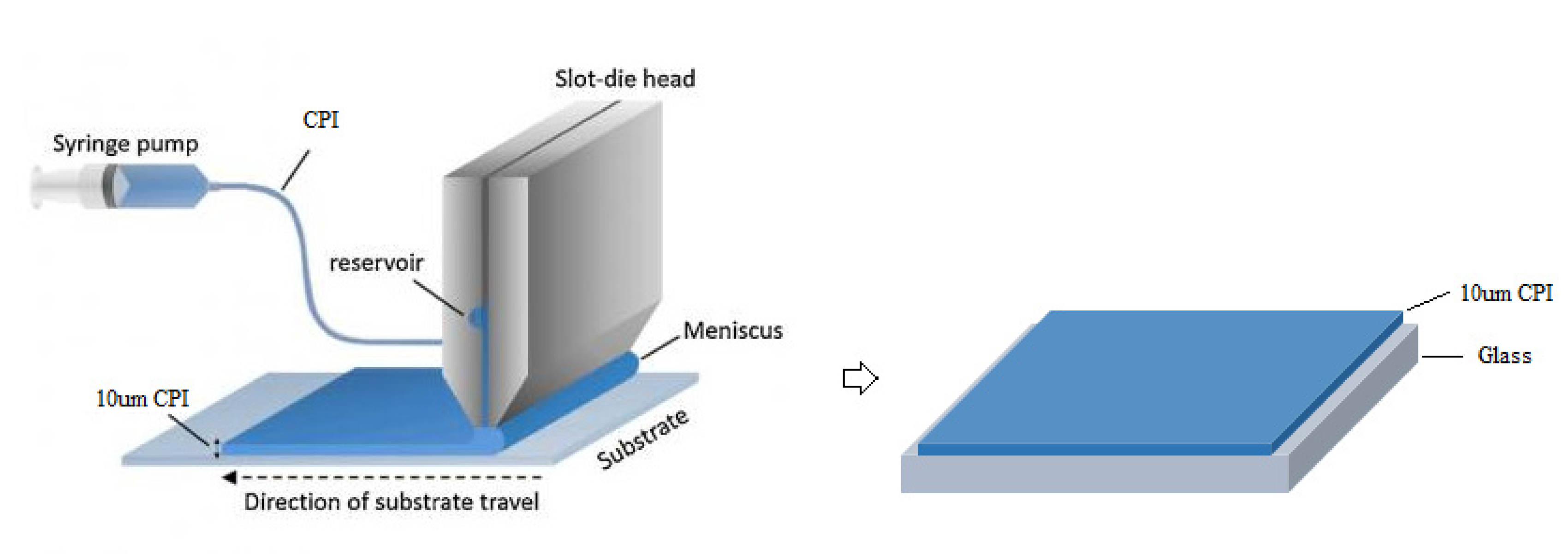
CPI films were prepared on glass carrier plates using the slot-die coating method. First, soda-lime glass substrates were ultrasonically cleaned with a 5% NaOH solution and deionized water, dried with N₂, and then CPI slurry was uniformly coated using a slot-die head at a speed of 5 mm/s. The coated samples were heat-treated in an atmospheric environment at 350°C for 1 hour to fully imidize and cure the CPI, ultimately obtaining free-standing flexible CPI films with a thickness of 10±0.5 μm.
Figure 1.
Fabrication process of 10μm-thick flexible CPI substrates.
2.2. ITO Film Preparation
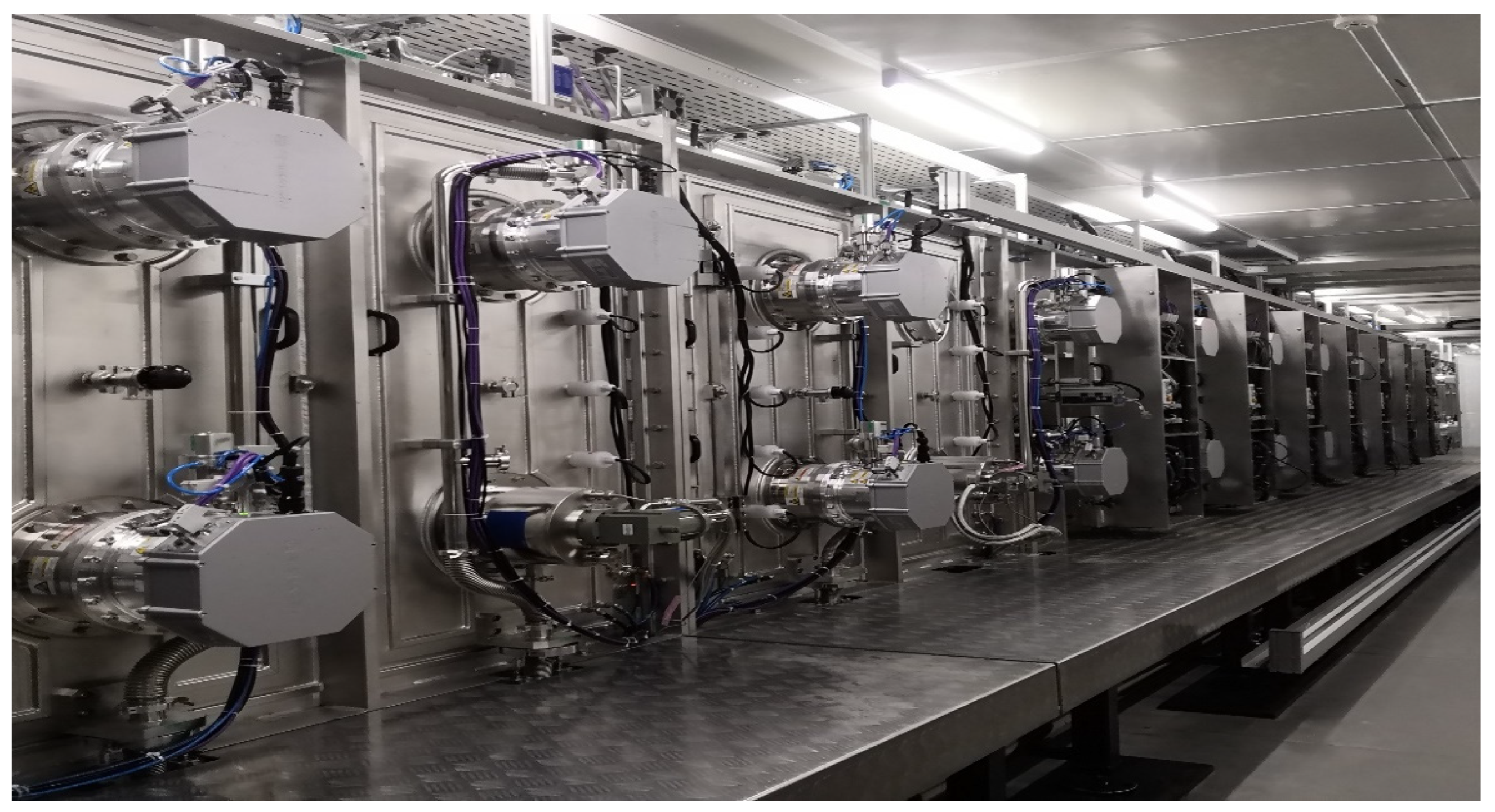
ITO films were deposited using a Leybold Optics Inline A1100V4 DC magnetron sputtering system. The sputtering target was a ceramic target (purity 99.99%) of In₂O₃:SnO₂ = 90:10 wt%. Before deposition, the chamber base vacuum was pumped to 1.0×10⁻⁴ Pa, the working pressure was maintained at 0.5 Pa, the Ar gas flow rate was 120 sccm, and the power density was 0.67 W/cm². By precisely controlling the substrate heating system, a series of samples were prepared within the temperature range of 30-300°C, with the film thickness uniformly controlled at 30±2 nm.
Figure 2.
Leybold Optics Inline A1100V4 DC magnetron sputtering system.
2.3. Heat Treatment Process
A atmospheric annealing furnace was used for post-annealing treatment of the samples. The deposited samples were heated from room temperature to 230°C at a rate of 5°C/min, held at that temperature in an oxygen atmosphere (flow rate 200 sccm) for 60 min, and then naturally cooled to room temperature.
2.4. Performance Characterization
X-ray diffraction (XRD, Shimadzu 7000) was used to analyze the film crystal structure; atomic force microscopy (AFM, Multimode Nanoscope IIIa) was used to characterize surface morphology and roughness; field emission scanning electron microscopy (FESEM, Zeiss Gemini 300) was used to observe the microstructure; a four-point probe tester (SDY-4) was used to measure resistivity; a Hall effect measurement system was used to measure carrier concentration and mobility; UV-Vis spectrophotometry was used to measure optical transmittance; X-ray photoelectron spectroscopy (XPS, PHI-1800) was used to analyze the chemical state of elements.
2.5. Bending Performance Test
Stress was applied to the sample through a fixture to bend it into an arc shape, treating the bent part as an approximate arc, which is the bending radius of the sample. Combined with the design requirements of touch screen products, this study adopted inward bending, meaning the formed arc has CPI on the outside and ITO on the inside. When adjusting the bending radius, one end of the sample was fixed, and the other end was bent with the movement of the fixture. The bending test setup is shown in Figure 3.
3. Results and Discussion
3.1. Temperature Dependence of ITO Film Optoelectronic Properties
To study the influence of coating process conditions before annealing on the electrical properties of ITO films on flexible CPI substrates, the following experiment was designed:

Table 1.
Parameters of ITO deposited by DC magnetron sputtering.
| Parameter | Value |
| Base Vacuum of chamber | 1.0*10⁻⁴ Pa |
| Process Pressure | 0.5 Pa |
| Power density | 0.67 W/cm² |
| Substrate temperature | 30~300℃ |
| Ratio of Ar/O₂ | 120:0 |
| Annealing temperature | 230℃ |
| Annealing time | 60 min |
In the experiment on the effect of ITO coating temperature before annealing on the resistivity of ITO after annealing, the Ar/O₂ ratio was maintained at 120:0. The coating temperature was increased from room temperature (30°C) to 300°C, preparing 11 groups of samples every 30°C. The samples were annealed at 230°C for 1 hour. The tested film thickness was 20nm. The relationship of the resistivity and transmittance of the ITO films is shown in Figure 4 below:
Figure 4 shows the variation of ITO film optoelectronic properties with deposition temperature. Notably, a non-monotonic trend was observed: when the deposition temperature increased from 30°C to 120°C, the resistivity after annealing decreased sharply from ~6000 μΩ·cm to 203 μΩ·cm; however, when the temperature continued to rise above 150°C, the resistivity反而 increased slightly. Hall effect tests showed that the carrier concentration of the sample deposited at 120°C reached 8.7×10²⁰ cm⁻³, and the mobility was 35.2 cm²/V·s, significantly better than samples prepared under other temperature conditions.
Transmittance tests shown in Figure 5 indicate that the visible light transmittance of all samples at a wavelength of 550 nm was higher than 85%, with the sample deposited at 120°C reaching 89.2%. (Note: The text mentions transmittance increasing to 91% with annealing temperature increase, but Figure 5 seems to show deposition temperature. This might be a slight inconsistency in the original text. The translation follows the figure caption and main description). The optical bandgap of the films blue-shifted with increasing deposition temperature, further analysis showed an increase from 3.75 eV to 3.92 eV, consistent with the Fermi level entering the conduction band due to the Burstein-Moss effect.
3.2. Bending Resistance Study
The bending radius was set to R=5mm, and the change in sheet resistance of the film after different numbers of bending cycles was measured. The change rate of sheet resistance for the ITO film over the same distance was tested and defined as ΔR/R₀, where ΔR = R - R₀. R is the sheet resistance at the current number of bends, and R₀ is the sheet resistance before the experiment.
For ITO films with a thickness of 30nm on CPI substrates annealed at 230°C for 1 hour, with substrate temperatures ranging from 30°C to 300°C (selecting one sample every 60°C), bending tests were conducted. The specific results are as follows:
As shown in Figure 6 above, the bending test results show that the substrate temperature significantly affects the ΔR/R₀ change rate of CPI-based ITO films. At a substrate temperature of 30°C, after 500 bending cycles, the initial sheet resistance change rate was already 16.4%, losing application value. At a substrate temperature of 90°C, ΔR/R₀ increased rapidly with the number of bending cycles, sharply rising to 41.7% at 4000 cycles. At 120°C and 150°C, after 100,000 bending cycles, the ΔR/R₀ change rates were 7.52% and 7.81%, respectively, possessing commercial use value*. *However, when the substrate temperature further increased above 210°C, the bending resistance decreased somewhat. Therefore, the optimal substrate temperature for ITO films with the best bending endurance is 120°C.
Some studies point out that stress concentration at defect points initiating cracks and delamination forming wrinkles are key factors leading to the decline of ITO conductivity [13]. During ITO film bending, due to stress concentration, microcracks first generate at defect points and extend along both ends in the direction of the bending roller axis, forming transverse cracks. As the number of bending cycles increases, the number of cracks increases, and the ITO at the crack surface peels off and sheds in fragments [14]. Cairns et al. pointed out that there is a corresponding relationship between the number of cracks per unit length n_d and the bending strain ε; n_d increases with the growth of ε, but n_d does not increase indefinitely, eventually tending towards a saturation value [15]. The number of cracks gradually stabilizes with the increase in bending cycles. Because the deeper ITO experiences less deformation and remains partially connected, retaining some conductive channels, the resistance change rate curve shows rapid growth initially, then tends to a relatively flat high-resistance state. The damaged ITO fragments at the crack sites suffer increased damage during repeated bending. Continuing to increase the number of bends will cause the ITO at the cracks to fall off, blocking the conductive channels and losing conductivity.
3.3. Microstructure Evolution Mechanism
XRD tests in Figure 7(a) show that regardless of deposition at substrate temperatures of 110°C, 150°C, 190°C, or 230°C, the ITO films still exhibit the cubic bixbyite structure of In₂O₃, and no diffraction peaks of SnO or SnO₂ appear, meaning Sn is incorporated into the crystal structure of In₂O₃. The crystal structure of the ITO films is polycrystalline. When the substrate temperature gradually increases from 110°C to above 190°C, the preferred crystal plane of the ITO films gradually changes from (222) to (400), while the diffraction peak intensities of the (222), (440), and (622) crystal planes gradually increase. Figure 7(b) shows that as the substrate temperature increases, the peak intensity ratio of (222) to (440) and (400) gradually decreases, while the peak intensity ratio of (440) to (400) first decreases and then increases, indicating that ITO crystals gradually grow in the <100> direction.
According to the Debye-Scherrer formula D=0.9λ/βcosθ, where λ is the X-ray wavelength (0.154 nm), β is the full width at half maximum (FWHM) of the diffraction peak [16], and the lattice constant calculation formula is 1/d² = (h² + k² + l²)/a₀², where (h,k,l) are the Miller indices, the microstructure parameters of the samples obtained from Figure 7(a) are as follows:
In ITO films, the radii of Sn⁴⁺, Sn²⁺, and In³⁺ ions are 0.69 Å, 0.93 Å, and 0.79 Å, respectively. From Table 2, it can be seen that as the substrate temperature before annealing increases, the lattice constant gradually decreases, and the grain size gradually increases. Since no oxygen was added during the experiment, the Sn in the ITO films was not fully oxidized, partially existing in the Sn²⁺ state. Due to the larger ionic radius of Sn²⁺, the lattice constant increases. Under oxygen-deficient conditions, even when the temperature reaches Ts, the lattice constant of the ITO film is still larger than the standard In₂O₃ value of 1.0118 nm. Therefore, insufficiently oxidized Sn²⁺ ions may exist in the ITO films. Y. Shigesato et al. proposed the Volmer-Weber model for ITO film growth, where ITO films grow gradually from small islands, and island density is affected by grain aggregation [17]. Before annealing, during ITO film sputtering, particles at higher substrate temperatures gain greater free energy, and their migration ability increases. In contrast, the migration ability of particles at lower substrate temperatures is reduced, forming fine islands. Therefore, the grain radius is smaller, the island density is higher, and grain boundaries increase. The movement of high-energy particles also leads to an increase in (400) plane intensity. Consequently, the resistivity of ITO before annealing decreases with increasing substrate temperature.
ITO films prepared at different substrate temperatures were annealed in an air environment at 230°C for 1 hour. The XRD structure after annealing is shown in Figure 8, and the grain size and lattice constant calculated according to the Scherrer formula are shown in Table 3.
From Figure 8, it can be seen that after annealing at 230°C for 1 hour, the ITO films deposited at substrate temperatures of 110°C and 150°C still predominantly exhibit the (222) plane, while the diffraction peak intensities of planes such as (211), (440), and (400) also gradually increase. Compared to ITO films prepared at substrate temperatures of 190°C and 230°C, the difference is not significant; all show a crystalline state after annealing. Data from Table 3 show that after annealing, the grain size of the (222) plane for ITO prepared at different substrate temperatures significantly increases, and the lattice constant also gradually approaches the size of standard In₂O₃ (~1.0118 nm).
XRD analysis reveals the temperature dependence of film crystallization behavior. Before annealing, the sample deposited at 110°C only shows a weak (222) diffraction peak, indicating the film is in a nanocrystalline state; the sample deposited at 150°C begins to show (400) and (440) diffraction peaks, presenting mixed crystallization characteristics; when the temperature rises above 190°C, the film is fully crystalline, and the preferred orientation changes from (222) to (400). After annealing at 230°C, all samples show good crystalline states, but the low-temperature deposited samples have a more uniform grain size distribution.
Calculating grain size based on the Scherrer formula found that the grain size before annealing increases with deposition temperature, but after annealing treatment, the final grain sizes of samples deposited at different temperatures tend to be consistent (~24 nm). This phenomenon indicates that the amorphous films deposited at low temperatures undergo more significant structural reorganization during the annealing process, resulting in a more uniform microstructure.
3.4. ITO Film Surface Morphology and Roughness Analysis
Figure 9 shows the AFM microtopography of ITO films deposited at substrate temperatures of 150°C, 190°C, and 230°C before and after annealing at 230°C for 60 minutes. As evident from the figure, significant differences exist between the microstructures of the annealed (Figure 9(a), (b), (c)) and non-annealed (Figure 9(e), (d), (f)) ITO films. The annealed ITO films exhibit a uniform granular morphology, whereas the non-annealed films show block-like particles with randomly oriented grains.
As the substrate temperature increases prior to annealing, the surface roughness (Ra) of the post-annealed ITO films gradually decreases, recording values of 1.24 nm, 0.756 nm, and 0.649 nm, respectively. It is worth noting that the grain sizes calculated from XRD data differ from the AFM observations. Studies by Z. Ghorannevis et al. suggest that grain height significantly influences the surface roughness of ITO films [18], attributing this effect to surface protrusions and step edges. Grain height, defined by the height of these protrusions and steps, is determined by the deposition and crystallization conditions during crystal growth. Therefore, although the grain size varies for ITO films prepared at different substrate temperatures after annealing, the similar crystal growth conditions on the surface lead to a consistent trend in roughness reduction with increasing substrate temperature. Higher substrate temperatures promote improved crystal structure and enhanced surface flatness during growth, thereby reducing surface roughness.
In addition to grain height, other factors such as annealing temperature, redox properties, and atmospheric conditions also affect the surface roughness of ITO films. Higher annealing temperatures facilitate crystallization and grain growth, consequently reducing roughness. Variations in redox conditions and annealing atmosphere—such as oxidative atmospheres removing surface defects and oxides, or reductive atmospheres reducing oxides and defects while promoting crystal growth and lattice refinement—also contribute to smoother surfaces.
Despite the lower surface roughness achieved with high-temperature deposition, the electrical performance of these films is comparatively inferior. This indicates that on flexible CPI substrates, surface roughness is not the dominant factor influencing electrical properties; instead, the deposition conditions play a more critical role.
3.5. Film Chemical State and Doping Mechanism
To reveal the chemical state evolution and doping efficiency mechanism of the annealed ITO films, high-resolution X-ray photoelectron spectroscopy (HR-XPS) was used to characterize the ITO film deposited at "110°C + 230°C atmospheric annealing for 60 min". Peak fitting using a Lorentz-Gauss mixed function was performed to analyze the chemical valence states and electronic structure of In, Sn, and O elements (Figure 10). Key analyses are as follows:
3.5.1. In 3d Orbital Chemical State
The In 3d orbital shows typical spin-orbit splitting features, split into In 3d₅/₂ (low binding energy side) and In 3d₃/₂ (high binding energy side), with a peak separation of approximately 3.3 eV (consistent with the standard spin-splitting spacing for In³⁺). The characteristic peak of In 3d₅/₂ is located at 444.6 eV, and In 3d₃/₂ is at 452.0 eV, both corresponding to the characteristic binding energy of In³⁺ in the In₂O₃ lattice. No peaks for In⁰ (~441.5 eV) or other low-valent In ions were observed, indicating that In exists solely as In³⁺ in the film and no reduction reaction occurred; only a weak asymmetric broadening was observed on the high binding energy side of In 3d₅/₂ (445.0-446.0 eV, marked as Inₓ⁺), attributed to weak interaction between surface In³⁺ and adsorbed oxygen, belonging to surface slightly oxidized non-lattice In, whose impact on overall electrical performance is negligible.
3.5.2. Sn 3d Orbital Chemical State
The Sn 3d orbital also shows significant spin-orbit splitting, with a peak separation between Sn 3d₅/₂ and Sn 3d₃/₂ of approximately 8.4 eV (consistent with Sn element spin-splitting rules). Peak fitting results show two chemical states of Sn in the film:
1)Effective doping state Sn⁴⁺: The Sn 3d₅/₂ characteristic peak is located at 486.7 eV, and Sn 3d₃/₂ is at 495.1 eV, corresponding to the doping configuration where Sn⁴⁺ substitutes for In³⁺ in the In₂O₃ lattice (Sn⁴⁺:In³⁺). Each Sn⁴⁺ can provide one free electron to the conduction band, making it the core source of carriers in ITO films. Its relative content directly determines the doping efficiency.
2)Ineffective doping state Sn²⁺: A clear shoulder peak appears on the low binding energy side of Sn 3d₅/₂ (485.2 eV), corresponding to the characteristic binding energy of Sn²⁺ (Sn 3d₃/₂ is at 493.6 eV). The ionic radius of Sn²⁺ (0.93 Å) is much larger than that of In³⁺ (0.79 Å), making it unable to effectively substitute for In³⁺ and enter the lattice. It only exists in interstitial states or surface adsorption states, not only failing to contribute carriers but also potentially acting as carrier scattering centers, reducing carrier mobility.
Peak integration results show that the relative content ratio of Sn⁴⁺/Sn²⁺ after annealing reaches 8.2:1, indicating that 230°C atmospheric annealing significantly promotes the oxidative conversion of Sn²⁺ to Sn⁴⁺, greatly improving doping efficiency – this directly correlates with the Hall test result of "carrier concentration reaching 8.7×10²⁰ cm⁻³ for the 110°C deposited sample".
3.5.3. O 1s Orbital Chemical State
The O 1s orbital can be fitted into three types of oxygen species, corresponding to different chemical environments. Their binding energies and physical meanings are as follows:
1)Lattice oxygen (O_L): Binding energy located at 530.0 eV, corresponding to O²⁻ strongly coordinated with In³⁺/Sn⁴⁺ in the In₂O₃ lattice (In-O-Sn/In-O-In bonds). It is a marker of the film's crystal structure integrity; the higher its relative content, the better the lattice order.
2)Oxygen vacancy-related oxygen (O_V): Binding energy located at 531.5 eV, corresponding to low-coordination O atoms around oxygen vacancies. Oxygen vacancies are another source of carriers in ITO films (each oxygen vacancy can provide 2 free electrons), but their excessive presence can lead to lattice distortion and increased carrier scattering.
3)Surface adsorbed oxygen (O_ads):Binding energy located at 532.8 eV, corresponding to OH⁻, H₂O, or O₂ molecules adsorbed on the film surface. It is unrelated to bulk electrical performance and only reflects the surface environment.
Peak integration results show that the relative content ratio of O_L/O_V after annealing is 6.5:1, indicating that the excessive oxygen vacancies introduced by low-temperature oxygen-free deposition (Ar/O₂=120:0) are moderately suppressed during 230°C atmospheric annealing (O_L proportion increases), forming a "controlled oxygen vacancy" state – retaining a certain number of carrier sources while avoiding scattering enhancement caused by lattice distortion, ultimately achieving an improvement in carrier mobility (35.2 cm²/V・s).
Comprehensive HR-XPS analysis reveals that the essence of the synergistic effect of "low-temperature deposition - post-annealing" is the precise regulation of chemical states – low-temperature oxygen-free deposition constructs an initial structure of "nanocrystalline + oxygen vacancies + Sn²⁺", and subsequent 230°C atmospheric annealing achieves two key transformations: ① Oxidation-driven Sn²⁺ → Sn⁴⁺, increasing effective doping concentration; ② Moderate oxidation reduces excessive oxygen vacancies, optimizing lattice order. Under the synergistic action of both, carrier concentration (n) and mobility (μ) are simultaneously improved, ultimately achieving a significant reduction in film resistivity (203 μΩ・cm).
4. Conclusion
Using the magnetron sputtering method and adopting the synergistic regulation strategy of "low-temperature deposition (110°C) - 230°C atmospheric annealing", high-performance flexible ITO conductive films can be prepared under conditions far below the CPI tolerance limit (Tg > 350°C). The optimal sample's comprehensive performance is: resistivity as low as 203 μΩ・cm, average visible light transmittance at 550 nm reaching 89.2%, surface arithmetic mean roughness (Ra) of 0.76 nm; under a bending radius of R=5 mm, the sheet resistance change rate after 100,000 bending cycles is < 10%, meeting the reliability requirements for flexible vehicle-mounted touch displays. The study found that the substrate temperature significantly regulates the initial crystallization state of ITO films – samples deposited at 110°C have a nanocrystalline structure, while samples deposited above 150°C gradually show a (400) plane preferred orientation; after 230°C annealing, all samples achieve good crystallization, but the nanocrystalline films deposited at low temperatures undergo more sufficient structural reorganization, resulting in uniform final grain size (~24 nm), lattice constant (1.01188 nm) close to standard In₂O₃ (1.0118 nm), and optimal crystal integrity. The core role of the annealing process is the complete oxidation of Sn²⁺ → Sn⁴⁺ (Sn⁴⁺/Sn²⁺=8.2:1) and the controlled adjustment of oxygen vacancies (O_L/O_V=6.5:1): the former increases the effective doping concentration, the latter optimizes lattice order, and together they synergistically achieve simultaneous improvement in carrier concentration (8.7×10²⁰ cm⁻³) and mobility (35.2 cm²/V・s), providing fundamental guarantee for electrical performance optimization. As the substrate temperature increases, the film Ra after annealing decreases from 1.24 nm (150°C) to 0.649 nm (230°C), but the electrical performance of high-temperature deposited samples resistivity increases, indicating that crystal quality and doping efficiency are the dominant factors for the electrical performance of flexible CPI-based ITO films, with surface roughness being only a secondary influencing factor.
This study elucidates the crystallization kinetics and doping mechanisms of ITO films under low-temperature conditions, breaking through the contradiction between "flexible substrate heat resistance - ITO performance". It provides a low-temperature technical path that can be industrialized for the preparation of high-performance transparent electrodes in fields such as flexible vehicle-mounted touch displays and wearable electronics, possessing both theoretical guiding significance and engineering application value.
References
- Chang J-H. Equibiaxially stretchable colorless and transparent polyimides for flexible display substrates[J]. Reviews on Advanced Materials Science. 2020;59:1-9.
- Longxia Yang, Xianjun Huang, Huating Wu, Yuanlong Liang, Mao Ye, Wencong Liu, Faling Li,1 Tao Xu and Haicheng Wang,. Silver Nanowires: From Synthesis, Growth Mechanism, Device Fabrications to Prospective Engineered Applications[J]. Engineered Science 2023, 23, 808.
- V. M. Silveira, M. S. Fuchs, D. K. Pinheiro, E. H. Tanabe and D. A. Bertuol, Recovery of indium from LCD screens of discarded cell phones[J], Waste Manage., 2015, 45, 334–342.
- Anna Isabel Hofmann, Eric Cloutet, Georges Hadziioannou. Materials for Transparent Electrodes: From Metal Oxides to Organic Alternatives[J]. Advanced Electronic Materials, 2018, ff10.1002/aelm.201700412ff. ffhal-01688624.
- Granqvist C., G. Transparent conductors as solar energy materials: A panoramic review[J]. Solar Energy Materials and Solar Cells, 2007, 91(17): 1529-1598.
- Lewis B. G., Paine D. C. Applications and processing of transparent conducting oxides[J]. MRS Bulletin, 2000, 25(8): 22-27.
- Z. Chen, W. Li, R. Li, Y. Zhang, G. Xu, H. Cheng, Fabrication of highly transparent and conductive indium-tin oxide thin films with a high figure of merit via solution processing[J], Langmuir. 29 (45) (2013) 13836–13842.
- H. Kim, C.M. Gilmore, A. Piqué, J.S. Horwitz, H. Mattoussi, H. Murata, Z.H. Kafafi, and D.B. Chrisey.Electrical, optical and structural properties of indium-tin-oxide thin Films for organic light-emitting devices[J]. J. Appl. Phys. 1999, 86, 6451-6461.
- S. Jung, J.Y. Seo, D.W. Lee, D.Y. Jeon, Thin Solid Films 445 (2003) 62.
- Shigesato Y., Takaki S., Haranoh T. Electrical and structural properties of low resistivity tin-doped indium oxide films[J]. Journal of Applied Physics, 1992, 71(7): 3356-3364.
- Ellmer K. Resistivity of polycrystalline zinc oxide films: current status and physical limit[J]. Journal of Physics D: Applied Physics, 2001, 34(21): 3097-3108.
- Yi Shen, Zhaochang Feng, Hanyan Zhang. Study of indium tin oxide films deposited on colorless polyimide film by magnetron sputtering[J]. 2020, Volume 193, 108809.
- Abdallah, Bouten P, de With G. Experimental study on buckle evolution of thin inorganic layers on a polymer substrate[J]. Eng Fract Mech. 2010;77:2896–2905.
- Yu Z., Li Y. G., Xia F., Zhao Z., and Xue W.. Properties of indium tin oxide films deposited on unheated polymer substrates by ion beam assisted deposition[J].Thin Solid Films 517, 5395–5398 (2009).
- Darran R. Cairns; Richard P. Witte, II; Daniel K. Sparacin; Suzanne M. Sachsman; David C. Paine; Gregory P. Crawford; R. R. Newton[J]. Strain-dependent electrical resistance of tin-doped indium oxide on polymer substrates.Appl. Phys. Lett. 76 (11) (2000) p. 1425.
- Cullity B. D., Stock S. R. Elements of X-Ray Diffraction (3rd Edition)[M]. Prentice Hall, 2001.
- Shigesato Y., Takaki S., Haranoh T. Electrical and structural properties of low resistivity tin-doped indium oxide films[J]. Journal of Applied Physics, 1992, 71(7): 3356-3364.
- Ghorannevis, Z., Akbarnejad, E. & Ghoranneviss, M. Structural and morphological properties of ITO thin films grown by magnetron sputtering[J]. J Theor Appl Phys 9, 285--290 (2015).
Figure 3.
Schematic diagram of a bending testing machine.

Figure 4.
Curves of ITO resistivity vs. deposition temperature before and after annealing.
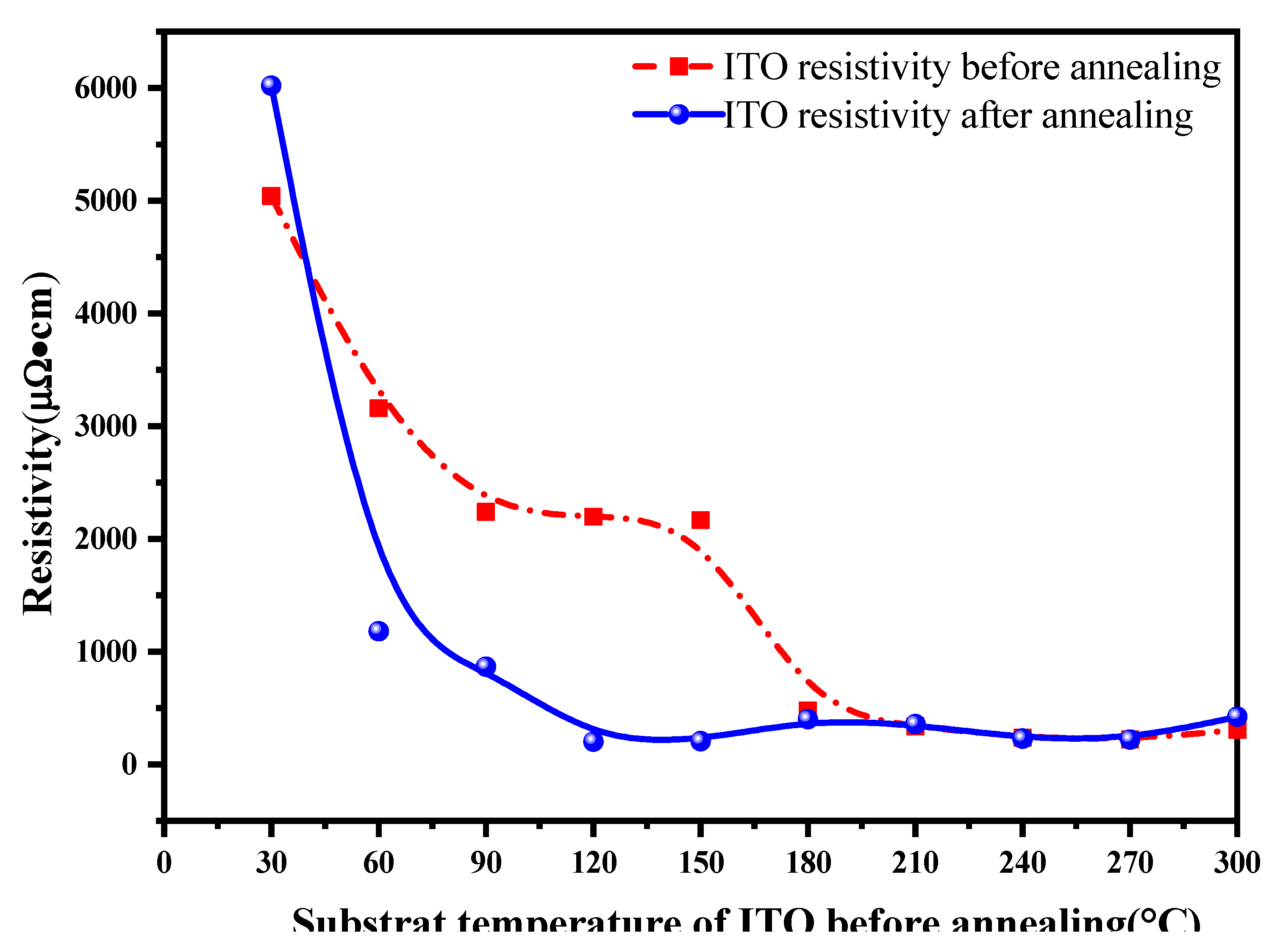
Figure 5.
Transmittance Curve of Post-Annealing ITO vs. Deposition Temperature.
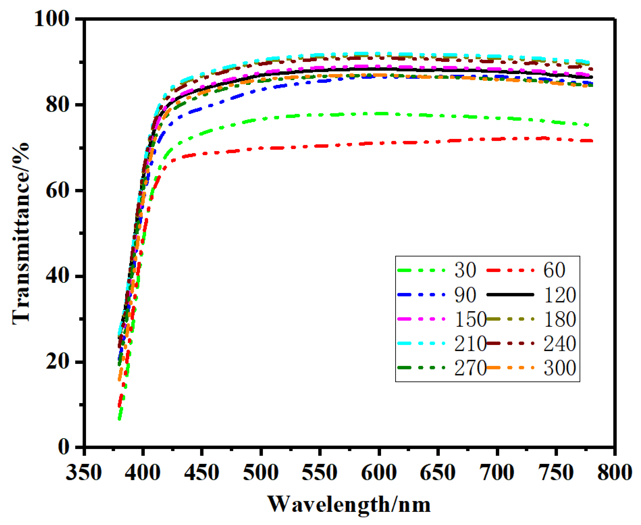
Figure 6.
Bending Cycles vs. Substrate Temperature Curve.
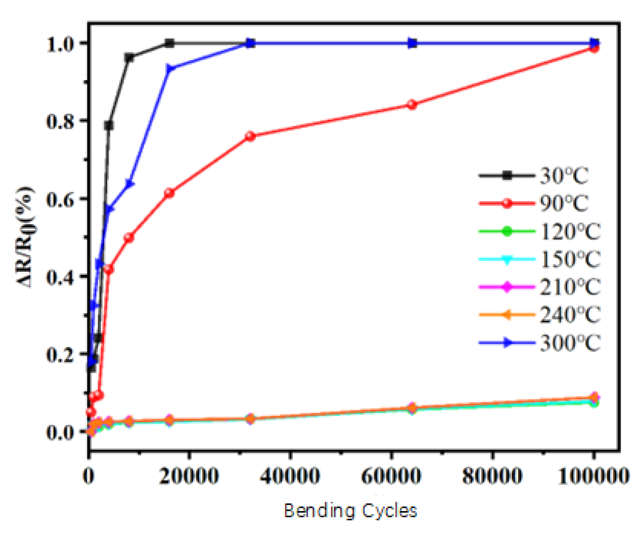
Figure 7.
XRD patterns of ITO films deposited at different substrate temperatures (a) and variation of ITO peak intensity ratio (b).
Figure 7.
XRD patterns of ITO films deposited at different substrate temperatures (a) and variation of ITO peak intensity ratio (b).

Figure 8.
XRD patterns of ITO films (prepared at different substrate temperatures) after annealing at 230°C in air for 1 hour.
Figure 8.
XRD patterns of ITO films (prepared at different substrate temperatures) after annealing at 230°C in air for 1 hour.
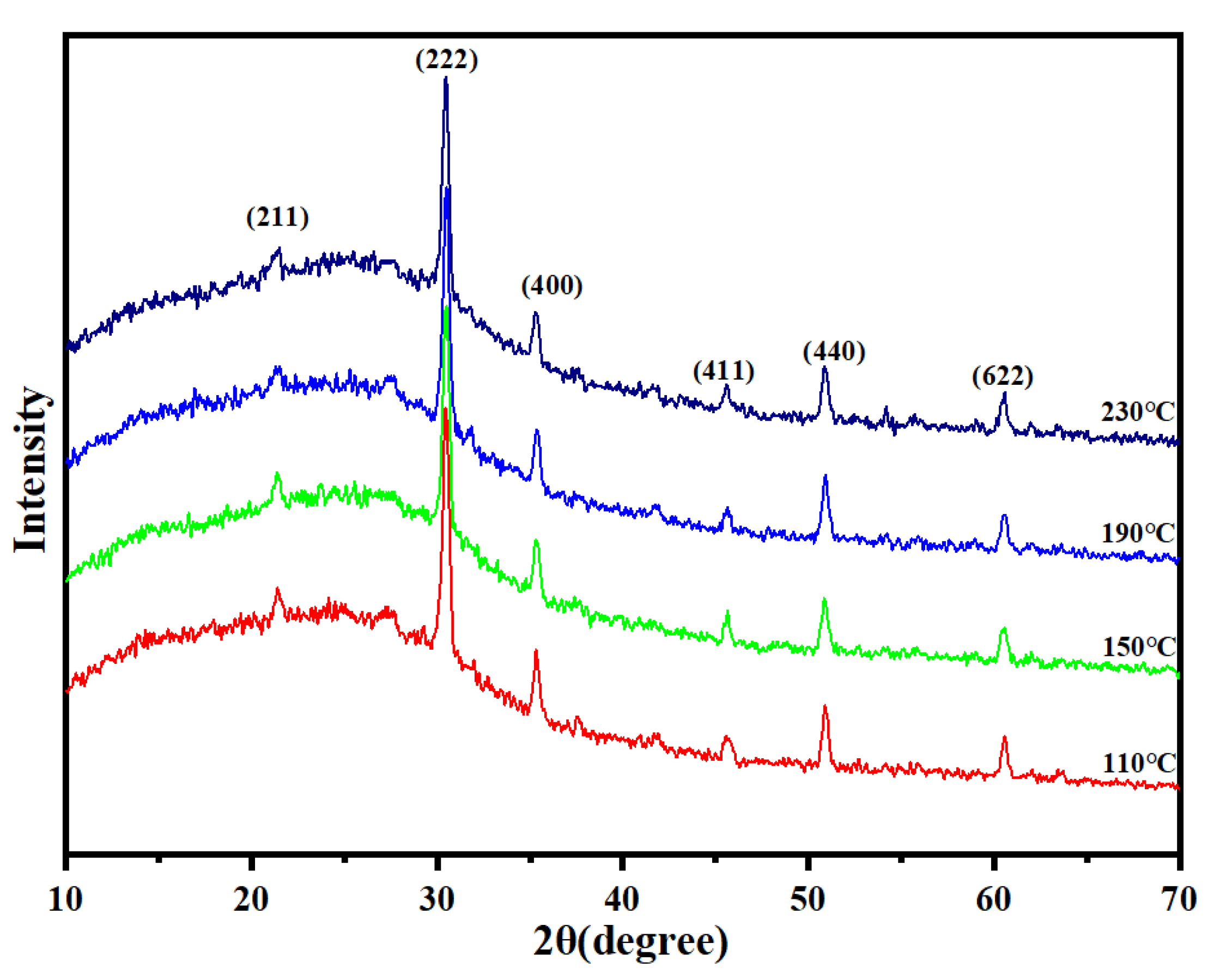
Figure 9.
AFM images of ITO films as-deposited and annealing with substrate temperatures of (a) 150°C, (b) 190°C, (c) 230°C.
Figure 9.
AFM images of ITO films as-deposited and annealing with substrate temperatures of (a) 150°C, (b) 190°C, (c) 230°C.
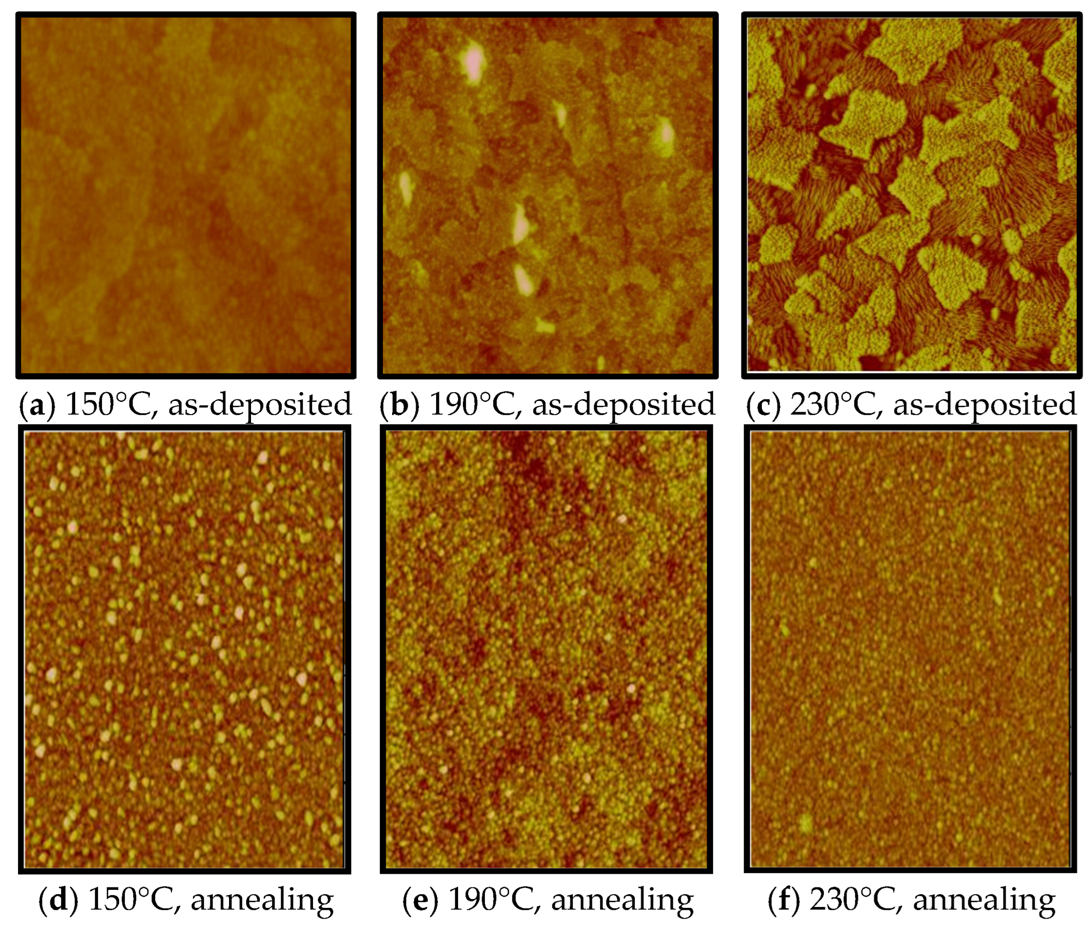
Figure 10.
XPS valence state analysis of ITO thin films annealed at 230°C for 60 minutes.
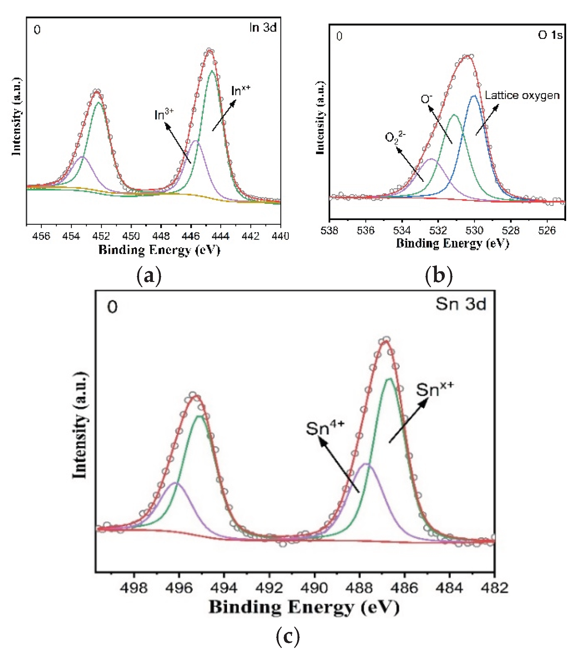
Table 2.
Microstructure of unannealed samples at different substrate temperatures.
| Substrate Temperature | (222) Grain Size (nm) | (222) d-spacing (nm) | (400) d-spacing (nm) | Lattice Constant a (nm) |
|---|---|---|---|---|
| 110℃ | 5.41 | 0.2929 | 0.2537 | 1.01468 |
| 150℃ | 10.13 | 0.2926 | 0.2534 | 1.01347 |
| 190℃ | 18.97 | 0.2921 | 0.2530 | 1.01196 |
| 230℃ | 20.48 | 0.2921 | 0.2530 | 1.01193 |
Note: Calculations for grain size examples provided in original notes: *1=0.9*0.154/0.861629*0.26*0.01745* *2=0.9*0.154/0.861629*0.45*0.01745* *3=0.9*0.154/0.861629*0.84*0.01745* *4=0.9*0.154/0.861629*0.91*0.01745*.
Table 3.
Microstructures of samples annealed at 230°C under different substrate temperatures.
| Substrate Temperature | (222) Grain Size (nm) | (222) d-spacing (nm) | (440) d-spacing (nm) | Lattice Constant a (nm) |
|---|---|---|---|---|
| 110℃ | 24.01 | 0.2921 | 0.2529 | 1.01188 |
| 150℃ | 23.63 | 0.2922 | 0.2530 | 1.01236 |
| 190℃ | 23.82 | 0.2921 | 0.2529 | 1.01193 |
| 230℃ | 24.51 | 0.2921 | 0.2529 | 1.0 |
Disclaimer/Publisher’s Note: The statements, opinions and data contained in all publications are solely those of the individual author(s) and contributor(s) and not of MDPI and/or the editor(s). MDPI and/or the editor(s) disclaim responsibility for any injury to people or property resulting from any ideas, methods, instructions or products referred to in the content. |
© 2025 by the authors. Licensee MDPI, Basel, Switzerland. This article is an open access article distributed under the terms and conditions of the Creative Commons Attribution (CC BY) license (http://creativecommons.org/licenses/by/4.0/).
Copyright: This open access article is published under a Creative Commons CC BY 4.0 license, which permit the free download, distribution, and reuse, provided that the author and preprint are cited in any reuse.


