

Submitted:
30 August 2025
Posted:
01 September 2025
You are already at the latest version
Abstract
The article presents developed and implemented hardware and software applications, according to original concepts related to structures and algorithms, in which the processing characteristics of the measurement system are implemented. Starting from a generous concept regarding the measurement path based on the literature review, the main emphasis of this paper is focused on the configuration of the device for measuring the power quality and validation of the processing characteristics of the tested devices. In the context of the analyzed device, a special attention is paid to the test studies, as well as to the issues of data transfer in the developed device and to the coordination of operation in this device. Some new ideas related to the analyzed issues and original findings are presented, analyzed and commented.
Keywords:
modeling and analysis
; measuring channel characteristics
; power quality assessment
; characteristics validation
1. Introduction
Most modern measurements are performed relay on electrical methods [1,2]. In the measurement system, the measured information is transmitted using a selected parameter of the electrical signal. This signal is processed in a way that provides the user with information about the value of the measured quantity, with acceptable accuracy of the measurement result.
The dominant part of the processes in the world around us is continuous. They can be assigned an infinite number of values differing by infinitely small increments. In addition to them, there are discrete phenomena, most often two-state, which from the point of view of measurements can be treated as a special case of the former. Further considerations concern the more general case of continuous processes.
In the measurement path, consisting of a number of elements and systems creating a chain for the measurement signal, functions related to the collection of measurement information from its source, conditioning of the signal carrying information and its processing are performed, according to the conditions of the systems enabling the measurement results to be made available to the user.
The first electrical measurement systems were implemented exclusively in analog technology, where measurement signals, as well as measurement results, are continuous [1]. Measurement information is most often transferred in them using instantaneous values of signals. Such measurement systems are still used, however, contemporary measurement technology has been dominated by systems based on digital technology, where measurement results are discrete. The expansion of digital measurement systems has its sources in three basic factors that give them an advantage over analog systems: processing, storing and transmitting both measurement information and measurement results. These operations on measurement signals in analog technology are performed with significant limitations [1], while commonly available digital technical means enable their easy implementation. Some information concerning this kind of solutions and their applications may be found in numerous publications, among others in [3,4].
The digital path for measuring an analog quantity consists of two basic parts: acquisition (signal processing) and estimation (digital data processing) (Figure 1). Information acquisition (data collection) is the first stage of processing, which involves collecting a signal from the source, conditioning it, transmitting it and converting it to a digital representation. Continuous information x(t) is converted into digital words Dx(ti) corresponding to the instantaneous values of the measured quantity at selected moments of time x(ti):
To recreate the instantaneous value of measurement information xm(ti), it is necessary to perform in the estimation part of the track an operation that is the opposite to the operations performed in the acquisition part:
The acquisition part of the DAQ (Data Acquisition) measurement chain, in which information is transmitted on instantaneous values of the signal x(t), at a basic level includes sensors and measuring transducers, signal conditioning systems, in many cases analog interfaces and analog-to-digital converters ADC (Analog-to-Digital Converter). The estimation part of the measurement chain, operating on digital data, performs digital data processing (software in microprocessor systems or hardware, e.g., in FPGA (Field Programmable Gate Array) systems), leading to determining the value of the measured quantity xm(ti) or derived quantities (using other additional data). Digital data processing can be performed with the participation of several independent functional blocks, e.g., a DSP (Digital Signal Processor) processor and a general purpose processor GPP (General Purpose Processor), which exchange information via digital interfaces. The configurations of both parts of the measurement chain remain in close dependence; the mathematical model of the acquisition part, describing its static characteristics in principle, is an unambiguous exponent of the tasks required for implementation in the estimation part of the chain, while simultaneously fulfilling the dynamic conditions related to the variability of the measured quantity. The correct operation of a digital chain for measuring analog quantities depends on the proper solution of two key aspects: the mathematical model implemented in the digital part of the chain and the coordination of information exchange between the functional blocks of this chain. The first issue includes determining the processing characteristics in the acquisition part of the chain, taking into account calibration issues, and defining algorithms to be performed in the digital part of the chain on this basis. The second issue requires resolving issues related to the synchronization of bits in the stream of transmitted data, the identification of information frames and the extraction of individual messages. The inclusion of programmable systems in the structure of the measurement chain, implementing the measurement function according to the given mathematical model, is associated with the need to develop methods for testing such a chain, in particular the functions implemented in programmable systems.
The issue of implementing measurements related to the systems of generating, transmitting and using electricity is related to the concept of “electric power quality assessment (EQA)” which covers a wide scope of topics, from signal acquisition using sensors and measuring transducers, through transmitting measurement information using analog or digital interfaces, to determining the values of indicators characterizing EQA and their registration and making them available to the user. It also includes research and assessment of phenomena accompanying the generation, transmission and use of electricity.
2. EQA Assessment Device Configuration
The Faculty of Electrical Engineering of the Maritime University in Gdynia has been conducting research for many years on the development of new methods and systems for assessing EQA. One of the components of this research was the development, production, testing and adaptation to measurement needs, as part of the project [5,6,7], of a device called “estimator/analyzer” (E/A). Its measurement functions focus on determining, indicating and recording electrical energy parameters (voltage, current, power and frequency values) and EQA indicators [8]. It also enables the recording of raw signal samples from the electrical network for further processing in an external system, e.g., a reference system using a PC (Personal Computer).
The main functional blocks of the developed device are shown in Figure 2. Voltages from the electrical network (3- or 4-wire) and phase currents from generating sets (up to three) are fed to the input terminals of the signal conditioning circuits, from where they are transmitted to the inputs of the ADC converters. Digital words from the ADC are sent to the DSP processor, where the EQA indicator values are determined. The input circuits of voltage signals from the electrical network supply the input lines of the ADC converters. The AD7656 (Analog Devices) [9] circuits were used as ADC converters. Data from the ADC converters can be sent via a three-line SPI (Serial Peripheral Interface) interface, synchronized with a single clock signal from the FPGA system. The FPGA system acts as an intermediary device between interface ports in different standards: ADC converters and DSP and GPP processors. The device uses a Spartan-3 XC3S1000 (Xilinx) FPGA [10], placed together with a DSP processor in the DSM STSL start-up module (Figure 3) [11]. The DSP functions are implemented by the TS201 TigerSHARC (Analog Devices) [12] system. It does not have SPI interface ports, available in both ADCs and GPPs, but can communicate via any of the four Link Ports using the LVDS (Low Voltage Differential Signaling) interface [13,14]. The LPC3250 processor (ARM9 family) [15] on the phyCORE-LPC3250 (NXP) base board is used as the GPP. This processor has standard ports for peripheral devices such as an SD (Secure Digital) card reader, LCD (Liquid-Crystal Display) and interfaces: UART (Universal Asynchronous Receiver/Transmitter), SPI and I2C (Inter-Integrated Circuit), USB (Universal Serial Bus) and Ethernet. GPP together with peripheral systems is the main element of the user interface (UI).
The configuration of the DAQ signal conditioning circuits used in the voltage channels is shown in Figure 4. Voltage dividers (VD), which divide input voltages with the KU factor, adjust the mains voltage level to an acceptable value in subsequent measurement channel blocks. The galvanic separation block (GS) ensures safe operation of the remaining E/A circuits. The eighth-order low-pass filter (LPF) is switched in the device between 10 and 100 kHz, depending on the current measurement function. The voltage follower (VF) provides the appropriate output resistance for this part of the measurement channel. The output signal is fed to the input of the ADC. Mains current measurements are performed with LFR 1/15 current probes (Power Electronic Measurements Ltd., Nottingham, UK) using Rogowski coils. The configuration of the DAQ circuits conditioning signals in the current channels is similar to the DAQ circuits used in the voltage channels, with the difference that there are no VD and GS blocks in the current channels. The signals from the current probes are fed directly to the inputs of the LPF blocks.
Since the amplification of signals in the GS, LFP and VF blocks is 1, the voltage at the ADC input can be described by the relationship:
where: UIN - voltage at the device input terminals (nominal effective values 230 V or 400 V); KU - voltage divider ratio (KU = 0.00383 V/V for UIN = 230 V and KU = 0.00221 V/V for UIN = 400 V).
The output code of the n-bit converter in the two’s complement numerical system, for the UADC input voltage, is described by the equations:
where in the used ADC [9]: n = 16; Uref = 2.5 V.
The values of the UIN signal samples are determined in the DSP processor (Figure 2 and Figure 3) based on digital data sent from the ADC and using the relationships obtained from the transformation (3), (4) and (5):
The EQA indicator values, determined in the DSP according to the selected measurement function, are sent to the GPP (Figure 2), where the user specifies how they are to be used in the form of visualization on the graphic display, recording or sending to other users. Optionally, it is also possible to send raw samples of network signals. The implementation of complex algorithms performed in real time requires the use of signal processors with appropriate properties. Signal processors are characterized by, among others, simultaneous access to instructions and data, hardware execution of signal processing operations and pipelined execution of program instructions. The ADSP TS-201 TigerSHARC processor used in the device as a DSP is a 128-bit processor, designed to perform operations on floating-point and fixed-point numbers, having, among others, dual sets of arithmetic logic units (ALU) for both types of operations, 24 Mb of internal DRAM (Distributed RAM) memory, integrated I/O systems, 14 DMA (Direct Memory Access) channels, 4 internal buses ensuring fast data exchange between memory and peripherals and other processor systems. It has four full-duplex Link Port systems that can work in parallel. These ports use LVDS interface lines in the physical layer [13,14], in which information (in 128-bit frames) is transmitted using a low-voltage differential signal in symmetrical lines using copper cables in a current loop configuration. The LVDS protocol in the DSP enables data transmission at up to 4 Gb/s in each port with very low power consumption. The Link Port can be configured to exchange data on one or four LVDS lines. Figure 5 shows signals on the LVDS interface lines.
The systems with which the DSP processor communicates in the developed device are equipped with interface ports in a different standard. Both the ADC converters in the device and the GPP processor used have SPI interface ports. Additionally, communication with each of these systems is possible via parallel interface ports, however, the possibility of using this interface was omitted in the research due to the high complexity of printed circuits in the bus connections between the device systems. It was decided to use serial communication due to the fulfillment of time regimes during data exchange via them, with lower complexity of connections [16]. SPI is a serial interface, fully bidirectional [17,18]. One of the devices connected by asymmetric interface lines acts as the Master system (Figure 6), outputs the SCK (Serial Clock) clock signal and manages the SS_N (Slave Select) lines used to activate one of the Slave systems. The SPI signal lines include: SCK, MOSI (Master Out Slave In), MISO (Master In Slave Out) and SS_N lines. According to the SPI standard, data is sent simultaneously in both directions in 8-bit frames (Figure 6), from the oldest to the youngest bit. Data transfer is synchronized with the rising or falling edge of the clock (depending on the configuration), and their setting is performed on the edge opposite to the one sending the data.
The transmission speed in SPI depends on the systems using this interface. In the case of both the ADC converter and the GPP processor in the developed device, the maximum communication speed was set at a level of several Mb/s. Communication errors occurred at higher speeds. As can be seen, this is in a large disproportion to the transmission speed via the Link Port interface in the DSP.
For data exchange between ports of different communication interfaces, the necessary conversion includes different amplitude and time parameters of the interface signals and the frame formats used in the respective interfaces. It should be noted that in communication interfaces, measurement data is not subject to any conversions in terms of their information value. The interface does not shape the course of the information processing characteristics in the measurement path, but is only a necessary technical means of ensuring the flow of information [19,20]. Figure 7 shows a configuration illustrating the use of FPGA systems to ensure the flow of information in the developed device [21,22,23]. In the FPGA, LUT RAM (Look-Up Table RAM), DRAM (Distributed RAM) and BRAM (Block RAM) buffers are used to store data. Continuous lines indicate the directions of flow of measurement information and configuration data, while dashed lines indicate auxiliary signals ensuring the coordination of operations performed in the device.
2.1. Test Studies
During the work on the constructed device, tests were carried out using alternative sources of data transferred between SPI and Link Port interface ports. Their aim was to verify the configuration of circuits coupling interface ports in different standards and to develop a method for data conversion between the data formats used in the frames of both interfaces. The course and results of preliminary tests of data conversion in FPGA between the SPI standard and Link Port are presented in [16,21] and in [24,25,26]. In the tests, data exchange was carried out between the Link Port of the ADSP TS-201 TigerSHARC signal processor and the SPI port of the Texas Instruments MSP430F149 microcontroller [17], acting as a general-purpose processor GPP in the system. The ADSP TS-201 EZ-KIT Lite development kit (Analog Devices, Norwood, MA, USA) [27], which contains two TigerSHARC signal processors, was used in the tests. The conversion between Link Port and SPI protocols was implemented in hardware, using the Xilinx Spartan 3 XCS200 FPGA [10] in the ZL10PLD [28] development module.
CLBs (Configurable Logic Blocks) are the basic FPGA logic configurator that can perform additional tasks, such as regular-length shift register and memory functions [10]. IOBs (Input/Output Blocks) enable bidirectional data exchange between CLB cells and I/O lines [10]. Each IOB block is equipped with pull-up and pull-down resistors that can be activated at will. This allows the use of different signal standards, e.g., LVDCI_15, LVDCI_25, GTP_DCI, HSTL_I_DCI, LVDS_25_DCI or SSTL18_I_DCI [16]. The idea of data conversion between interface standards implemented in the FPGA in the test system is shown in Figure 8. A single Link Port frame consists of 16 SPI frames. The example data contained in one Link Port frame (128 b) and the same data distributed in SPI frames (8 b) are symbolically presented.
The design and simulation of the operations of the designed circuits were carried out in the Xilinx ISE WebPack programming environment, which allows the creation of an FPGA configuration program, among others, in the VHDL language. Figure 9 shows a schematic configuration of the FPGA circuit implementing data conversion between the TigerSHARC Link Port and the SPI port of the GPP processor (MSP430F149 Texas Instruments). With clock signal frequencies differing by several orders of magnitude and different frame lengths in both standards, the conversion circuit is “transparent” for data, i.e., data transfer between ports takes place without interfering with their content [16]. The transmission between TigerSHARC and GPP is initiated after the FPGA sets the signal on the ACK line, after which TigerSHARC issues the rx_clk clock (125 MHz) and sends the rx_data data. The data is sent on both edges of the clock signal, from the least to the most significant bit in the frame (0 to 127). In the SPI interface, the GPP processor is configured as Master, so it issues the clk_spi clock (800 kHz) and initiates transmission in both directions. Data is received and sent at the same time in both devices. In both GPP and FPGA, data is set on the rising edge of the clk_spi clock, and is read on the falling edge. Data is transmitted in 8-bit frames from the oldest to the youngest bit (from 7 to 0). Data sent on the rx_data line from the Link Port is written to the BRAM at the rx_clk clock. This signal is also controlled by the address counter, which controls the order of data writing. Data on the MISO line is output from BRAM to GPP under the control of the clk_spi clock and with the participation of the address counter. The next Link Port frame can be received after data is output from BRAM to the GPP SPI port (ACK ready signal from FPGA to Link Port)).
Communication between the GPP microcontroller and the TigerSHARC microprocessor begins with sending data to the MOSI line from the GPP SPI port to BRAM at the clk_spi clock. This data is written to BRAM in a similar way to communication in the reverse direction, under the control of the appropriate address counter. Sending tx_data data from BRAM to Link Port is synchronized with the tx_clk and tx_clk270 (100 MHz) clock signals. They are generated in the DCM (Digital Clock Manager) block by multiplying the frequency and appropriately shifting the phase of the 50 MHz clock signal clk generated in the FPGA. Transmission is started after the frame is completed, on the ACK signal from the Link Port.
The problem of a different order of data sent by the Link Port (from the least to the most significant bit in 128-bit frames) than the order of sending data from the SPI port (from the most to the least significant bit in 8-bit frames) was solved by changing the order of their reading from the BRAM. In both communication directions, data is read in the reverse order to the order of their writing.
In addition to tests of basic functional components consisting in observing internal signals output to the FPGA output lines, the following were carried out:
- testing the correctness of duplicating the frequency of clock signals and shifting them in phase in the DCM block,
- testing the correctness of BRAM addressing for both directions of transmission controlled by the clk, rx_clk and clk_spi clocks,
- checking the correctness of data sent to BRAM from TigerSHARC and from the SPI port,
- testing the transfer of data emulated in BRAM to TigerSHARC and to the SPI port.
The results of the tests were used in the configuration of the developed device for testing EQA. It should be noted that the operations performed in the interfaces using FPGA in the developed device differ fundamentally from the operations in the test system.
2.2. Data Transfer in the Developed Device
The developed device uses the AD7656 circuits from Analog Devices [9] as ADC converters. Their inputs are supplied with signals from voltage followers (Figure 4). A single AD7656 circuit (Figure 10) contains six 16-bit ADC converters, controlled by pairs (CONVST A-B-C) and storing the processing results in three registers assigned to each pair. Digital data can be output from the system via a 16-bit parallel port DATA/CONTROL LINES (under the control of additional lines and ) or via three serial interface lines, modeled on the SPI standard (DOUT A-B-C), controlled by an external clock signal SCLK. The conversion time of the analog signal sample to digital form in each converter is constant and equal to 3 µs. The end of the processing cycle is signaled on the BUSY line and then it is possible to start outputting ready data. In the measurements of the line voltages, when the antialiasing filter frequency is set to fLPF = 100 kHz, the ADC channels V1, V3 and V5 are used. The set of data in the output buffers is shown in Figure 11. With this selection of the ADC channels of the AD7656, only 16 SCLK cycles are necessary to output the buffer contents using three SPI lines, which takes about 0.94 µs (Figure 11). This solution allows processing of instantaneous values of ADC input signals at a speed of up to about 250 kS/s in each of the three channels.
From the point of view of ADC processing, the device realizes two operating options:
- sampling of line voltages at a speed of 210 kS/s in three voltage channels,
- sampling of three voltages and six currents at a speed of 25 kS/s in nine ADC channels.
In the second case, six channels of the second AD7656 circuit are additionally used.
Figure 12 shows the operations performed during the recording of raw voltage samples from the power system. The ADC converters’ work cycle (start: signal from FPGA on CONVST A-B-C lines) includes parallel processing of three voltage samples, placing the results in output buffers and sending them via SPI to the FPGA. ADC-FPGA communication is performed on slightly different principles than in the previously shown test system. The serial interface used in the ADC system is a modified version of the original standard. The Master system functions are performed by an external system and only the MISO lines are used, three interface lines controlled by a common clock signal. The SCLK clock signal is generated in the FPGA. The next ADC work cycle starts according to the set processing frequency (only voltage measurements with speed fADC = 210 kS/s or voltage and current measurements with speed fADC = 25 kS/s), asynchronously to further operations on digital representations of the processed signals and sent to buffers in the FPGA and then to the DSP.
The Spartan-3 XC3S1000 (Xilinx) [10] FPGA plays an important role in the measurement chain of the device, enabling connections between the main functional blocks. The IOB lines between the ADC and the FPGA are configured as single-ended 3.3 V SPI lines. Data from the ADC is delivered to the DSP via a 4-line Link Port (LVDS) interface between the FPGA and the DSP, where the IOB lines are configured as symmetrical lines (Figure 5). For data exchange between the DSP and the GPP, the 1-wire Link Port lines connecting the DSP to the FPGA are also configured as symmetrical lines. The lines connecting the FPGA to the GPP were configured as unbalanced in the 2.5 V voltage standard.
To maintain data flow between different interfaces, the FPGA must convert between the functions (protocols) implemented in their data link layers and change the formats of frames transmitted on these interfaces [29,30,31,32,33,34].
Inside each configurable logical CLB in the FPGA there is a LUT (Look-Up Table) element. It is usually used to implement logical functions, but it can be reconfigured as a random access memory RAM cell that can store 16 bits of data. These elements can be combined into a larger RAM, called distributed RAM - DRAM. Another type of memory available in FPGA is BRAM. It is a dedicated dual-port memory containing several kilobytes of RAM. A typical FPGA contains at least several such blocks. Both single-port and dual-port BRAM modules can be used. In two-port BRAM modules, both ports can be controlled by clocks with different frequencies. In the case of using selected ADC, DSP and GPP circuits as the main functional blocks, the FPGA implementation was crucial for the successful implementation of the developed measuring device [19].
The LPC3250 circuit, as a GPP processor, normally supervises the operation of peripherals in the user interface circuit and enables data exchange with the DSP via FPGA, using the SPI interface, the port of which in GPP acts as the Master device.
The following section presents the operations carried out in FPGA for the option of measuring three voltages in the power network at a speed of fADC = 210 kS/s (ADC processing cycle every tADC = 4.76 µs) due to the critical time relations between the operations for this option in relation to the option of measurements in nine ADC channels (ADC cycle every tADC = 40 µs). For both options, data from the current cycle is processed in the DSP in real time, during the next ADC processing cycle.
For each ADC cycle, data is transferred via three SPI lines to three LUT RAM buffers in the FPGA. In the next step, data is rewritten from the LUT RAM to the DRAM memory in the FPGA, and then to the DSP processor using 4 lines in the LVDS standard (Figure 13). Data sent to the DSP is contained in 128-bit frames, so the data from the LUT RAM must be reformatted and placed in another part of the FPGA.
The operation of transferring data from the LUT RAM to the DRAM memory is controlled by two synchronized clocks (Figure 13). The first one, clkL, controls the output of data from the LUT RAM memory, while the second one, clkD, manages the writing of individual bits to the DRAM P and DRAM N memory blocks. The clkL frequency is twice as high as the clkD frequency. The input to DRAM P is controlled by the rising edge of clkD, while the write to DRAM N is performed on the falling edge of clkD. The capacity of each DRAM is 64 bits. Each digital representation of the set of analog samples is sent separately to the DSP processor, so the contents of the LUT RAM are transferred to the set of DRAM blocks while changing the data layout. Data is output from the registers in the following sequence: first from LUT A, then from LUT C, and finally from LUT B. The order of bits in the ADC and LUT RAM buffers is shown in Figure 14. Figure 15 shows the layout of data bits in the DRAM registers. The data representing the samples from the ADC cycle, with a volume of 2x24 bits, is sorted so that it is ready for transmission to the DSP via a 4-wire LVDS interface.
The IOB elements at the multiplexer output form a 4-line LVDS port. Each line consists of two differential lines (marked in Figure 15 as “+” and “-”), the first of which transmits a signal corresponding to the value of a given bit, and the second to the negated value of this bit. In the DSP processor memory, data is collected in the form of 4 kB blocks, of which 3.06 kB is occupied by sample data. In addition to the data from ADC processing, additional information data is recorded there. After collecting 510 frames containing data sets from subsequent ADC cycles in the DSP memory, a 4 kB data block is sent to the GPP processor (Figure 12). In the first phase, the 4 kB data block is sent to the FPGA using a single-line LVDS interface, and then from the FPGA to the GPP, data is sent via a standard SPI interface, managed by GPP with the Linux operating system. Data reception begins after detecting an edge on the SYNC line, which signals the end of data buffering from the DSP. This line ensures coordination of communication via the SPI port between the FPGA and GPP. In the original concept of the device, this coordination was performed by software: reading data from the FPGA via SPI to the GPP was initiated by a timer in the GPP. Following an interrupt, generated in the GPP approximately every 200 ms, a 4 kB data block was initiated from the FPGA to the GPP via SPI. However, transmission operations from the DSP to the FPGA and further from the FPGA to the GPP are mutually asynchronous processes. As a result, during data reading from the FPGA to the GPP, the data in the FPGA could be overwritten by data contained in subsequent frames from the DSP. The introduction of hardware coordination (SYNC line) and abandoning software coordination in the GPP eliminated the possibility of such an event occurring. Data received in GPP are then saved in the flash drive memory via USB port, under the control of software included in the Linux kernel [21]. Figure 16 shows the sequence of data output from buffers in the ADC to LUT RAM buffers in the FPGA and their conversion in the FPGA and transmission to the DSP [19,21,24,25,26]. It illustrates the time relations between the processes carried out in the developed device, starting from analog signal conversion to digital form in the ADC converter (at a speed of 210 kS/s) to data recording in 4 kB frames in the SRAM memory of the DSP processor. As mentioned earlier, the time of analog signal conversion to digital form in the ADC converter is constant and equal to tCONV = 3 μs. The ttr time, i.e., the time of data transfer to buffers in the FPGA via SPI from three ADC channels, depends on the clock frequency synchronizing the data reading from the ADC via SPI. In the device conditions, it is 943 ns. The tACQ data acquisition time in FPGA consists of processing the instantaneous signal values into digital form and sending the processing results to FPGA [19,21]:
During the next processing cycle in the ADC converter (tCONV = 3 µs), data is rewritten from the LUT RAM buffers in the FPGA to a pair of DRAM buffers in this system. Transferring 46 bits of data (data from one ADC cycle) requires a tRAM time of less than 300 ns. The data from a single ADC cycle (total: 16-bit data from three ADC channels (48 b)), which make up the content of the Link Port frame, is placed in a pair of DRAM buffers. The data block is sent from the DRAM memory using the LVDS protocol to the DSP processor. In this operation, data in a 128-bit frame, divided between four LVDS interface lines, is transmitted at a rate of 200 Mb/s. The tRAM-DSP time required to transfer one frame is:
where: lp – number of bits transmitted in a single LVDS line (lp =32 b), vs – bit transfer rate in a frame from FPGA to DSP (vs =200 Mb/s). In the DSP processor memory, 510 data frames from LVDS are collected, where each 128-bit frame contains 48 b of 16-bit data from three ADC channels. In the DSP, a block of 3.06 kB of data from the ADC is created from the received frames, and with additional information - a block of 4 kB of data. These frames are collected in the DSP processor memory during tBUF (10):
where: nr – number of frames recorded in the DSP processor (nr = 510), tADC – time step of sampling (corresponds to the ADC processing frequency fADC=210 kS/s)).
Figure 17 shows the time relations between the operations of transferring a block of data stored in the DSP processor memory to the flash drive portable memory. Data transmission begins after buffering 4 kB of data in the DSP and proceeds in the buffering cycle of subsequent 4 kB blocks of data in the DSP.
Through the 1-line Link Port interface, controlled by the clock signal from the FPGA (clock from the DSP, f = 125 MHz), 4 kB data are sent from the DSP processor to the FPGA in frames containing lp=128 bits at a speed of vs = 250 Mb/s. A single frame is sent in time tD-F1:
To send a 4 kB block in 250 128-bit frames, the following time is necessary:
where: nr – number of frames sent from the DSP to the FPGA (nr=250).
After receiving a 4 kB data block in the FPGA, a signal is set on the SYNC line, which is used to synchronize data reception in GPP. Data transfer is performed under the supervision of the software in GPP, which initiates the clock signal fSPI = 16 MHz, controlling the transmission to GPP via a standard bidirectional SPI port. The transmission time of a single 8-bit frame can be expressed by the Formula (13):
where: lb – number of bits in the frame (8 b), vb – transmission speed (16 Mb/s).
The time of sending a block of 4 kB of data in nr=500 frames is:
The block of received data is buffered in the GPP memory and then written to the flash drive portable memory using USB port drivers in the Linux environment. The results of the study of writing to the USB port medium indicated the need to buffer larger memory blocks in GPP before writing them to the USB, especially for raw data, delivered in 4 kB blocks every approx. 2.43 ms (tBUF). This allows for increasing the time interval between writing sessions. The time interval when sending EQA indicator values is approx. 200 ms. Table 1 shows the percentage of erroneous frames saved in the flash drive memory, in relation to all frames sent from the DSP, for different time intervals between transmission from the DSP to the GPP of successive 4 kB frames. It follows that the recording sessions should take place no more often than every tUSB=18 ms. This corresponds to a block of data stored in the GPP with a volume of approx. 30 kB.
2.3. Coordination of Operations in the Device
In order to clearly present the issues discussed in this part of the self-report, in relation to the coordination/synchronization operation in the functioning of the device, the conceptual apparatus was adopted in accordance with the definition [35], where the concept of coordination means “the efficient course or functioning of something”, and synchronization is “coordination in time of at least two phenomena”. Therefore, synchronization is a special case of coordination of operations.
In measurement and control systems, the transmission of digital data between devices, as well as between functional blocks of a digital device, is usually carried out using standard digital interfaces. Unlike analog interfaces, in digital interfaces, data can be saved before sending and thus restored in the event of their loss during transmission to the receiver. Currently, serial interfaces are of particular importance, and this technology is developing dynamically.
Electrical signals propagate in a copper cable at a speed of about 2∙108 m/s, which means that the signal sent from the transmitter appears in the receiver 100 m away after a time of about 0.5 µs. Signals carrying data in a digital interface are subject to distortion due to the limited bandwidth of the communication channel, as well as attenuation, also dependent on distance. Additionally, the operation of interface ports is controlled by local clock signal generators with limited stability of their frequency. These factors mean that in digital interfaces, special attention is paid to synchronization in data exchange processes. This applies to both interfaces operating in asynchronous and synchronous modes. The basic difference between them is that in asynchronous mode, the receiver clock is synchronized once on the edge of the signal carrying the data frame and then autonomously controls the decoding of subsequent bits in the frame, while in synchronous mode, the receiver clock is synchronized with the transmitted transmitter clock throughout the transmission of the data frame.
The process of synchronizing digital data transmission usually takes place in several stages [19]:
- bit synchronization (implemented in the physical layer of the interface),
- frame synchronization (data link layer),
- information synchronization (application layer).
Bit synchronization enables correct decoding of subsequent bits of the frame by identifying them in the signal at the correct time. In asynchronous interfaces, receiver clock synchronization is achieved on the edge of the received signal carrying the start bit. The receiver clock is previously set to the same frequency as the transmitter clock. In the receiver, after detecting the edge, the receiver clock phase is appropriately adjusted, and then the receiver clock signal becomes a reference for determining the time moments at which decoding of subsequent bits from the signal carrying them takes place, in relatively short frames transmitted asynchronously. The limited frame length results from the limited stability of the receiver clock frequency in relation to the transmitter clock frequency.
The receiver clock in the synchronous interface is continuously synchronized with the transmitter clock. Although the source of transmission synchronization is usually the transmitter’s clock, in short-range interfaces (when the signal delays in the interface lines are negligible in relation to the clock signal period), e.g., in SPI, synchronization can be performed using any of the clocks of the communicating devices. In long-range interfaces, the source of the synchronization signal is usually the transmitter’s clock (the delay in the data lines is similar to the delay of the clock signal). The clock signal can be transmitted on a line independent of the data lines or on a common line together with the data, using a selected so-called self-synchronizing code. A data sequence encoded in this way contains information that allows the extraction of a clock signal (from the transmitter) for synchronization of the receiver’s clock.
Frame synchronization is necessary to correctly recognize the beginning, end and remaining fields of the frame based on a continuous sequence of bits transmitted on a clock-synchronized signal and is performed after bit synchronization and error-free decoding of individual bits (a bit synchronization error, including e.g., loss of a data bit, causes a frame synchronization error). Frame synchronization for a given communication standard is performed by referring the stream of reconstructed bits to a reference frame, which allows for the identification of the preamble contained in the introductory part (a characteristic sequence of characters that will most likely not appear in the rest of the frame) in synchronous transmission or only the start bit in an asynchronous transmission frame and subsequent fields of the frame, including the user data field.
Information synchronization is based on time coordination and purposeful and proper use of user data transmitted in subsequent frames, in a manner corresponding to the functions performed in the system. This involves combining data sent in multiple frames and, in some cases, the need to organize their order.
The problem of coordinating operations in the measurement chain does not, however, apply exclusively to the interfaces used. Transferring data between functional blocks is one of the operations in the measurement chain. Another problem is the mutual cooperation of blocks and operations that create the measurement channel.
Figure 18.a shows a measurement chain in which individual operations (or part of them) are coordinated by a dedicated, central control unit CCU (Central Control Unit). This unit, based on information about the status of individual operations, manages the work of individual blocks of the measurement chain and coordinates their cooperation.
Figure 18.b illustrates the case of measurement paths with distributed coordination, in which the interaction between different functional blocks is based on the mutual coordination of independently performed operations and coordination of directly exchanged information between blocks. There is no superior unit coordinating the exchange of data between cascaded functional blocks. This type of process coordination is most commonly used in measurement paths, where the continuity and smoothness of information stream processing and its recording are important. After processing data in a selected functional block of the device, the start of data transfer to the next functional block must be coordinated between these blocks. Coordination can be carried out programmatically, using software running in the selected block (often under the control of time systems), or hardware, based on the state of operations or systems. Coordination of operations in the exchange of information between the functional blocks of the developed device consists in ensuring smooth data transmission between ADC and GPP and managing them in the UI data recording and indication system (Figure 7). Figure 19 shows the basic blocks of the device along with the times of execution of individual operations [19].
The coordination of operations in individual blocks of the measurement chain consists in the fact that in order to maintain the smoothness and consistency of the information flow, the condition relating to the relationship between the times of execution of the relevant operations must be met: the time of execution of specific operations is critical and cannot exceed the time of execution of other operations.
The first limitation concerns the time interval tADC between analog signal samples at the ADC input in relation to the minimum acquisition time tACQ (8), i.e., tADC ≥ tACQ, which can be written as:
Fulfilling this condition enables correct transfer of digital data from the ADC to the LUT RAM buffer in the FPGA. Before the next processing cycle is completed, i.e., in the next tADC time segment, the data must be transferred from the LUT RAM input buffers to the DRAM in the FPGA and then transferred to the DSP using 4-line LVDS before the next portion of data from the LUT RAM, so the following condition must be met:
The data is buffered in the DSP during tBUF. They must then be sent to BRAM (buf-RAM 2) in the FPGA via 1-line LVDS before the DSP collects another 4kB buffer of data provided by 4-line LVDS and then sends from buf-RAM2 to GPP via SPI:
However, this requires the use of two independent 4kB buffers in the DSP to avoid overwriting subsequent data transferred from the ADC at tADC=4.76 µs before sending it to the GPP. Data in GPP is collected, as it arrives via SPI, in blocks of at least 30 kB, ensuring their error-free recording via the USB port, with an appropriate time interval between subsequent recording sessions. This does not interfere with the smoothness of other operations in the device.
3. Validation of Processing Characteristics
Each manufacturer of measuring instruments ensures that they meet the applicable standards and that the uncertainty of measurement results obtained with their use does not exceed the established levels. The accuracy of measurement results depends on several factors, including the stability of processing characteristics, the correctness of measurement algorithms implemented in the instrument and the quality of its calibration. The term “calibration” can be defined as: “a test during which known measurement values are fed to the input of a device and the corresponding output readings are recorded under specified conditions” [36]. In engineering [37], the term “validation” means confirmation that the instrument meets the needs of its users and it defines the action or process of making something officially or legally acceptable or approved. Calibration and validation share the common goal of ensuring that the instrument operates as intended. These are interrelated but distinct processes and at a basic level of meaning, these concepts can be defined as follows:
- calibration ensures that the measurement accuracy of the instrument corresponds to a known standard,
- validation ensures that the system meets specified functional assumptions. It is difficult for the user of a measuring instrument to assess the correctness of its indications during measurement operations. He can only rely on the declarations of the instrument manufacturer or its legalization certificate.
This part focuses on presenting the methods of validating the characteristics of the developed instrument, implemented in combination with calibration procedures. The configuration of additional systems necessary to implement these procedures is discussed in relation to separate parts of the measurement chain, in which information is processed in a system and program manner.
The configuration of each chain in a digital system for measuring analog quantities can be illustrated in a simplified form shown in Figure 20 [20,38,39,40]. The correctness of the measurement result is determined by two main parts of the chain, DAQ data acquisition and DDP (Digital Data Processing). The assessment of the characteristics of the measurement chains of the developed instrument was made taking into account these two parts of the chain.
Measurement information in the DAQ part of the track is transferred via instantaneous values of analog signals, and the processing of these signals is carried out in the system (in the analog track). The course of characteristics in the DAQ system may change, because this part of the measurement track is susceptible to the influence of many external factors, such as temperature, electromagnetic interference or aging changes of the elements. Calibration of the DAQ part is based on determining its actual signal processing characteristics. In the DDP part, information in the form of a digital representation of signals from the DAQ part, after their collection and conversion in the ADC converter, is presented in the form of a digital data stream. Data processing in this part of the track is carried out in software (in general, it can also be carried out in the system, e.g., using FPGA). The DDP characteristic, describing data processing according to specific algorithms, remains basically unchanged, it is practically insensitive to factors that affect the characteristics of the DAQ part. Validation of the DDP characteristic consists in checking the correctness (and possibly correcting) of the measurement algorithms performed in this part of the track. Calibration of the DAQ part is easy to perform. It consists in determining the relationship between the output signal and the input signal (under steady-state conditions) in the entire range of the input signal. Calibration of the input analog circuits, starting from voltage dividers (for three voltage channels) and Rogowski coils (for six current channels) to ADC converters (Figure 2 and Figure 4), was performed using standard AC voltage and current sources. Figure 21 shows an example characteristic obtained as a result of calibrating one of the current probes used, together with the designation of its trend line. Figure 22 shows the deviation of the trend line from the probe characteristic. The absolute value of this deviation (Δapprox) slightly exceeds the value of 0.8 A. Considering the range of the current probe (peak current 3 kA), this is an acceptable value in the considered application. The trend line equations obtained in the calibration procedures of the DAQ part of the measurement chain were used in the DDP part to scale the digital data in the relevant measurement chains.
Processing the data obtained from DAQ for the standard test signal St in DDP allows to determine the actual DAQ characteristics and correct the data at the DAQ output obtained for individual samples of the measurement signal Sm, as well as to determine the corrected result together with an estimate of its uncertainty - additional operations performed in DDP are shown in Figure 23. A detailed description of the procedures and the calibration circuit is presented e.g., in [41].
Digital data processing (DDP) algorithms used to determine the values of individual EQA parameters in the developed device are based on the use of discrete wavelet transform (DWT), fast Fourier transform (FFT), discrete Fourier transform (DFT) or chirp Z-transform (CZT), performed in a complementary manner [20,42,43]. Namely, wavelet coefficients at appropriate levels of wavelet decomposition are used as input data to various procedures used to calculate effective values and coefficients in the Fourier series, in combination with the transient monitoring algorithm. The main elements of the measurement algorithms are shown in Figure 24. These operations are implemented in the DSP processor (Figure 2).
The sine qua non condition for the correctness of measurement operations involving the device is the appropriate use of the calibration results of the device’s DAQ circuits. Regardless of this, the accuracy of determining individual EQA coefficients also depends on the correctness of the algorithms used in the DDP part of the measurement channels. Tests on their correctness were carried out using four configurations, with the participation of additional operations and systems shown in Figure 25 [20]. The procedures for assessing the correctness of the algorithms are implemented in applications running on a PC. Distinguishing the DAQ and DDP parts in the measurement channel allows the use of different test signals and calibration techniques to assess the measurement properties of the device.
In the system shown in Figure 25a, preliminary tests of the device algorithms were carried out. Software design, as well as preliminary verification of the measurement algorithms implemented in the E/A software, were carried out using the EVAL-TS201S-EZKIT Analog Devices evaluation module [27], equipped with two TigerSHARC processors, the same type as the DSP used in the E/A device. On the other hand, the verification of the measurement algorithms of individual EQA coefficients was carried out entirely using standard digital data sets. These studies were of significant importance for the process of starting the developed device, despite the limited set of test data, which did not include various measurement conditions. As a result, the designed and tested software was installed in the DSP processor in the device. Figure 25b shows the configuration in which the device calibration algorithms were validated using standard analog test signals. The calibration and validation procedures apply to both parts of the measurement chain: DAQ and DDP. The standard signal source used was a three-phase Chroma 6590 Programmable AC Power Source (Chroma ATE Inc., Taipei Hsien, Taiwan) [44]. The same signal source was used in the systems shown in Figure 25b,c. In the experimental system shown in Figure 25b, the measurement results obtained from the device are evaluated in an estimation system using a PC, taking into account the parameters of the test signal from the Chroma generator. Another way to check the measurement characteristics of the device uses recorded raw signal samples. In the experimental system shown in Figure 25c, for stationary test signals, digital representations of raw samples of these signals are recorded in the PC. For the same test signals, the values of individual EQA indices are determined in the device. In the estimation system, supported by a PC running a software package (independently tested on the basis of reference data), the recorded raw samples are processed and then the calculated indices are compared with the indices obtained in measurements with the tested device.
Table 2 contains the measurement results of the parameters of the three-phase triangular signal (experimental system as in Figure 25b), generated using a programmable alternating current source Chroma (declared values of Urms, U1 and THD for the standard triangular signal DST017 from the generator waveform library) [44], in relation to the results obtained from the tested device and as a result of processing the raw samples in the PC application (experimental system as in Figure 25b).
In the tests carried out in the system shown in Figure 25d (and also in Figure 25c), the use of input reference signals is not required. The test signals were simultaneously fed to the inputs of the tested device and to the inputs of the reference device. The reference device was developed using the PCIeXtensions for Instrumentation (PXI) platform (National Instruments Corporation, Austin, Texas, USA), equipped with appropriate peripherals and software in the form of a virtual device designed in the LabVIEW environment. Figure 26 shows sample results of calibration of phase voltage measurement paths, and shows the differences (ΔUrms) between the effective values measured by the tested device and in the PXI system.
Table 3 contains absolute errors ΔUrms representing deviations between the effective values of the phase voltages measured by the E/A device and the PXI system, obtained during the calibration of the device for different mains voltage frequencies, as well as relative (percentage) errors δ, assuming the value indicated by the PXI device as the actual voltage value. The collected results indicate that the main source of errors were systematic effects resulting from inaccuracies in the calibration of the processing characteristics of the measurement channels (the channels are subject to recalibration or the ΔUrms values can be used to correct the results). The largest change in the ΔUrms value with a change in frequency for each phase does not exceed Δmax = 0.2 V. It can be attributed to random effects and, assuming a uniform distribution of these deviations, the standard uncertainty u can be calculated from the formula:
In summary, all the applied methods of assessing the characteristics of the measuring path are reliable in relation to the developed device. The obtained results of experimental verification are positive, within the permissible tolerance range. However, based on the obtained results, it is not possible to draw conclusions regarding the correctness of the algorithms in different measurement conditions and their necessary modifications in order to improve the measurement accuracy.
As part of the research on the measurement properties of the developed device, an additional validation method was proposed, similar to the method shown in Figure 25c, in which the sets of source data supplied to the DSP and PC may differ. Individual JEE coefficients are calculated in the DSP based on signal samples collected in time windows lasting about 200 ms (10 periods of network waveforms with a frequency of about 50 Hz), which, with a sampling period of tADC=4.76 µs, consists of over 42,000 samples of three network voltages (or in the second mode of the device operation, with tADC=40 µs, about 5,000 samples of three voltages and six currents). The proposed method of validation of measurement algorithms, applicable to the developed E/A device (and probably other devices), is based on the assumption that the data set used to calculate the coefficients in the tested device is the same as the data set used in the reference system. This assumption is met if a set of measurement data in the form of network signal samples, as well as the results of processing this set of data in the DSP in the form of EQA indicators, are saved and jointly delivered to the PC as a reference system for calculating the appropriate coefficients and comparing them with the indicators determined in the DSP (Figure 27).
Figure 3 shows the resources of the DSM STSL module used in the developed device. The module is equipped with 128 MB of synchronous dynamic random access memory SDRAM (Synchronous Dynamic RAM). This memory was not used in the device operations due to the sufficient capacity of the internal memory of the DSP processor (24 Mb) for the calculations of the EQA coefficients. The proposed concept of validation of measurement algorithms assumes the use of SDRAM memory (Figure 3) to store a set of samples from the ADC converter, but only those that were used by the DSP processor to calculate the EQA coefficients, together with the designated coefficients. The capacity of the SDRAM memory allows for the accumulation of data from several 200 ms time windows. For example, to store data collected from samples from three voltage channels, processed in the ADC converter at a speed of 210 kS/s, no more than 256 kB of memory for one window is needed. In order to validate the built-in algorithms, the original source data together with the processing results in the DSP are sent to an external system. In this way, for real measurement signals it is possible to evaluate the software algorithms executed in the DSP. The set of samples recorded in SDRAM, after being sent to the PC, is used for independent off-line calculation of the appropriate JEE indicators, which are then compared with the values of these indicators calculated in the DSP. The reference system is developed in the LabVIEW environment. A simple criterion is used to validate the tested algorithm implemented in the DSP:
where: - the value of the indicator calculated in the DSP/A; - the value of the indicator determined in the estimation operation in the PC; Δi- the permissible error specified for the tested algorithm; i - the indicator identifier. The imperfection of measurement algorithms often results from the rounding, simplifications and approximations used, and their optimization can contribute to improving the properties of the measuring device. More detailed descriptions of some other aspects of data processing in the measurement chain of the E/A device are analyzed in [19,20,34,38,39,40].
4. Discussion
In the wide variety of articles available describing the design and operation of measurement systems, it’s difficult to find a procedure describing how to develop a software algorithm that can be run on a microprocessor device, using data from an analog-to-digital converter (ADC) to estimate and recover the value of a measured analog quantity. In [3] one can find a description of the complete model of the measurement operation in a digital measurement device. It consists of two main parts: mathematical model of conversion (corresponding to the acquisition part of the measurement channel) and mathematical model of reconstruction (corresponding to estimation part).
The presented article, as a case study, describes a complete procedure for developing a mathematical model of the DAQ part of the measurement chain for the adopted system configuration of the device. In this part, the measurement information is carried out on the electric signals, depending on the measurement task in three or nine measurement channels, and finally is converted in the ADC to the digital representation. The digital data from all measurement channels are transferred by means of the FPGA, configured to unify different peripherals, to the Tiger SHARC DSP processor.
The mathematical model of the DAQ part is the basis for designing software algorithms in the DDP part designated to determine the values of individual EQA indicators. They are calculated after normalizing the digital samples of momentary values of measured network signals. In many cases, indicators are determined in indirect measurements, as a process involving one or more direct measurements [4].
The EQA indicators determined also include indicators unavailable in many known solutions of similar devices for assessing PQ in industrial power networks. These include indicators related to the specific conditions in shipboard power networks, associated with large frequency oscillations of network signals (more broadly: “soft networks”), the need to measure currents in at least three channels (from separate generating sets), and the determination of the proportionality of active and reactive power flows (or non-active power).
The article presents reliable test results of conversion systems between various interface standards using FPGA and the implementation of these systems in communication channels of the designed device [19]. The goal of the tests was to develop a data conversion method in the FPGA that ensures smooth data transfer from the ADC to the DSP, as well as from the DSP to the GPP processor, including maintaining the timing regimes for operations on the SPI and Link Port interfaces, as well as for the utilized FPGA resources, while maintaining the transparency of these operations with respect to the information content of the transmitted data stream. As part of the tests, the execution times of operations resulting from the conversion of data frames from the source interface to the target interface format were determined. The proper coordination of operations in the FPGA, confirmed by the test results, was finally validated in the form of a properly functioning device in its final configuration. It also includes an in-depth analysis and verification results of the time relations between the processing and information transmission operations in the device [19]. The conducted analyses have shown that all operations related to data format processing and transmission are performed in the FPGA with sufficient time margins to ensure the safety and reliability of these operations.
The article also presents developed procedures for calibrating the device’s measurement channels and multi-variant methods for validating the processing characteristics of the hardware and software parts of the device’s measurement paths [20]. It is important to emphasize the universal nature of the proposed approach to calibrating individual functional blocks of measurement chains, both in their hardware and software components, as well as the multi-variant validation methods presented, which can be adapted to the specific characteristics of the measurement chain elements. It is worth mentioning that a simple criterion (19) was proposed and successfully applied to validate the tested algorithm implemented in DSP.
Finally, it should be emphasized that the presented review is the result of many years of research on the construction of systems for determining the indicators of the electrical quality and the initial idea of this article is to confront theoretical knowledge regarding the research topic under consideration with the principles of good engineering practice.
5. Future Directions
The completed project of an electricity quality estimator/analyzer (E/A) is not a static project and the possibilities of further progress of the developed and proven technology are being investigated. The experience gained while working on the device and during its use allows for the formulation of conclusions regarding what improvements, modifications or extensions are possible or planned for the device.
The developed device, although dedicated to measurements specific to ship power systems, can be used for electrical power quality assessment in land systems. The set of implemented functions and measurement options covers legal provisions related to measurements in land electrical power networks and additionally meets the specific requirements governing EQA measurements and assessment in ship power networks.
The E/A instrument is used on an ongoing basis for occasional assessment of EQA indicators on seagoing ships in ports, during tests related to emergency situations in the ship’s electrical power system, for preparing expert opinions, as well as during sea trials and periodic inspections.
Within the developed structure of the device, ongoing research and development efforts are focused on the integration of advanced self-diagnostic features. It is assumed to consist in examining the stability of the characteristics of the acquisition part of individual measurement channels, based on data additionally collected in the external memory of the DSP processor and then processed in an external system in the form of post-analysis to verify the parameters of these characteristics. An important goal of these activities is to maintain an appropriate level of measurement accuracy. Expanding the device with algorithms for detecting interference sources in the network and trend analysis for predictive detection of power quality deterioration is also being considered. The introduction of automatic reporting and alerting functions for exceeding permissible parameter levels is also planned. The metadata collected in these operations can constitute the basis for further research using AI algorithms.
Based on the experience gained so far in using the E/A device, a general conclusion can be drawn about its good metrological properties, as well as positive operational features resulting from the mobility and universality of the device.
Certification procedures for the device are being considered, as well as the development of a stationary version of the device in collaboration with an external partner. This could provide new instrumentation for continuous monitoring of EQA parameters in ship systems. The goal is to increase the operational safety of ship systems and improve diagnostic capabilities for electrical energy generation and use systems. In the longer term, the device could become a component of a smart grid, supporting activities related to improving energy efficiency and power supply reliability.
Author Contributions
Conceptualization, R.M. and J.M.; methodology, R.M. and J.M.; software, R.M.; validation, R.M., J.M. and B.P.; formal analysis, R.M.; investigation, R.M. and B.P.; resources, R.M.; data curation, R.M..; writing—original draft preparation, R.M.; writing—review and editing, R.M., J.M. and B.P.; visualization, R.M.; supervision, R.M. and J.M.; project administration, R.M.; funding acquisition, J.M. and B.P. All authors have read and agreed to the published version of the manuscript.
Funding
This research received no external funding.
Data Availability Statement
No new data were created or analyzed in this study. Data sharing is not applicable to this article.
Acknowledgments
The authors have reviewed and edited the output and take full responsibility for the content of this publication.
Conflicts of Interest
The authors declare no conflicts of interest.
Abbreviations
The following abbreviations are used in this manuscript:
| ADC | analog-to-digital converter |
| ALU | arithmetic logic unit |
| BRAM | block RAM |
| CCU | central control unit |
| CLB | configurable logic block |
| CZT | chirp Z-transform |
| DAQ | data acquisition |
| DCM | digital clock manager |
| DDP | digital data processing |
| DFT | discrete Fourier transform |
| DMA | direct memory access |
| DRAM | distributed RAM |
| DSP | digital signal processor |
| DWT | discrete wavelet transform |
| E/A | Estimator/Analyzer of an electricity quality |
| EQA | electrical power quality assessment |
| FFT | fast Fourier transform |
| FPGA | field programmable gate array |
| GPP | general purpose processor |
| GS | galvanic separation |
| I2C | inter-integrated circuit |
| IOB | input/output block |
| LCD | liquid-crystal display |
| LPF | low-pass filter |
| LUT | look-up table RAM |
| LVDS | low voltage differential signaling |
| MISO | master in slave out |
| MOSI | master out slave in |
| PC | personal computer |
| PQ | power quality |
| PXI | PCIeXtensions for Instrumentation |
| RAM | random-access memory |
| SCK | serial clock |
| SD | secure digital |
| SDRAM | synchronous dynamic RAM |
| SPI | serial peripheral interface |
| SS | slave select |
| THD | total harmonic distortion |
| UART | universal asynchronous receiver/transmitter |
| UI | user interface |
| USB | universal serial bus; |
| VD | voltage divider |
| VF | voltage follower |
References
- Tumanski, S. Principles of electrical measurement; Tylor&Francis: New York/London, USA/UK, 2006. [Google Scholar]
- Nawrocki, W. Distributed measurement systems; WKL: Warszawa, Poland, 2006. [Google Scholar]
- Morawski, R.Z. Technoscientific Research. Methodological and Ethical Aspects; Walter de Gruyter GmbH: Berlin/Boston, Germany/USA, 2019. [Google Scholar]
- Mari, L.; Wilson, M.; Maul, A. Measurement Across the Sciences. Developing a Shared Concept System for Measurement; Springer Nature Switzerland AG: Cham, Switzerland, 2021. [Google Scholar]
- Mindykowski, J.; Tarasiuk, T.; Masnicki, R.; Szweda, M.; Gorniak, M.; Gorniak M. Universal power quality analyzer/estimator - part II, design and technical implementation. Scientific Papers of Gdynia Maritime University 2010, 66, 21–36. [Google Scholar]
- Mindykowski, J.; Tarasiuk, T.; Masnicki, R.; Gorniak, M.; Szweda, M. Experimental results of the universal power quality estimator/analyzer version 2.00. Measurement Automation Control 2013, 59, 341–344. [Google Scholar]
- Mindykowski, J.; Masnicki, R.; Hallmann, D. Acquisition of data from ADC using an FPGA. In Proceedings of the XX IMEKO World Congress, Busan, South Korea; 2012; pp. 1–4. [Google Scholar]
- Mindykowski, J. Assessment of electrical power quality in ship systems with converter systems. Shipbuilding and Shipping Publishing House 2001, Gdansk, Poland. [Google Scholar]
- Analog Devices, AD7656/AD7657/AD7658, Data sheet, Rev. D, 2010. Available online: https://www.analog.com/en/products/ad7656.html (accessed on 10 July 2025).
- Xilinx, Spartan-3 FPGA Family Data Sheet, Product Specification, Application Note DS099, 2005. Available online: https://docs.rs-online.com/5d58/0900766b80db5578.pdf (accessed on 10 July 2025).
- Kaztek Systems. Available online: http://www.kaztek.com/ (accessed on 7 April 2017).
- Analog Devices, ADSP-TS201 TigerSHARC Processor Hardware Reference, Rev. 1.1, 2005. Available online: https://www.analog.com/media/en/dsp-documentation/processor-manuals/396096833ts201_hwr.pdf (accessed on 10 July 2025).
- Xilinx, Analog Devices TigerSHARC Link Port, Application Note: Spartan-II and Spartan-3 Families, Virtex and Virtex-II Series, XAPP634 (v1.2), 2004. Available online: https://www.yumpu.com/en/document/read/16447144/xilinx-xapp634-analog-devices-tigersharc-link-application-note (accessed on 10 July 2025).
- Texas Instruments, LVDS Owner’s Manual, 4th ed., 2008, Available online:. Available online: https://www.ti.com/lit/ug/snla187/snla187.pdf?ts=1708266335350&ref_url=https%253A%252F%252Fwww.google.com%252F (accessed on 10 July 2025).
- Phytec, phyCORE-LPC3250, System on Module and Carrier Board Hardware Manual, 2009. Available online: https://datasheet.datasheetarchive.com/originals/crawler/phytec.com/aae1e9289399335b4978b6f13faa1b07.pdf (accessed on 10 July 2025).
- Masnicki, R.; Hallmann, D. Data conversion between Link Port and SPI interfaces. Measurement Automation Control 2011, 57, 1466–1468. [Google Scholar]
- Texas Instruments. MSP430x1xxx Family User’s Guide; 2004. (accessed on 10 January 2023).
- Xilinx. CoolRunner Serial Peripheral Interface Master, Application Note 348 (v1.2), 2002. (accessed on 10 January 2023).
- Masnicki, R.; Mindykowski, J. Coordination of operations in registration channel of data from electrical power system. Measurement 2017, 99, 68–77. [Google Scholar] [CrossRef]
- Masnicki, R. Validation of the measurement characteristics in an instrument for power quality estimation – a case study. Energies 2017, 4, 1–16. [Google Scholar] [CrossRef]
- Masnicki, R.; Hallmann, D. Application of FPGA in power system data acquisition. In Proceedings of the XLIV International Conference of Metrologists (MKM), Ustron-Wrocław, Poland; 2012. [Google Scholar]
- Masnicki, R.; Hallmann, D. Data acquisition from ADC using FPGA. Measurement Automation Control 2012, 11, 912–915. [Google Scholar]
- Mindykowski, J.; Masnicki, R.; Hallmann, D. The implementation of FPGA for data transmission between ADC and DSP peripherals in the measurement channels for power quality assessment. ACTA IMEKO 2013, 2, 49–55. [Google Scholar] [CrossRef]
- Masnicki, R.; Hallmann, D. Time dependencies in the data recording system from the electrical power system. Scientific Journals of the Faculty of Electrical and Control Engineering at the Gdańsk University of Technology 2014, 38, 45–48. [Google Scholar]
- Masnicki, R.; Hallmann, D. Coupling different interface standards using FPGAs. Scientific Papers of the Gdynia Maritime University 2014, 85, 16–25. [Google Scholar]
- Masnicki, R.; Hallmann, D. Analysis of time relations in the power system data recording system. Scientific Papers of the Gdynia Maritime University 2014, 85, 7–15. [Google Scholar]
- Analog Devices. ADSP TS-201 EZ-KIT Lite Evaluation System Manual, Revision 3.1, 2007. Available online: https://www.analog.com/media/en/technical-documentation/user-guides/303064930adsp_ts201s_ez_kit_lite_manual_rev._3.1.pdf (accessed on 10 July 2025).
- Kamani, dipPLD module with XC3S200 chip. Available online: https://dl.btc.pl/kamami_wa/zl10pld.pdf (accessed on 10 January 2023).
- Mindykowski, J.; Masnicki, R.; Hallmann, D. The strategies of data recording in power quality parameters measuring instrument. In Proceedings of the 20th IMEKO TC4 International Symposium and 18th International Workshop on ADC Modelling and Testing, Benevento, Italy; 2014; pp. 635–640. [Google Scholar]
- Masnicki, R.; Mindykowski, J.; Hallmann, D. The Time Relationship in Registration of Data from Electrical Power System. In Proceedings of the EPE 2014 - International Conference and Exposition on Electrical and Power Engineering, Iasi, Romania, October 2014; pp. 1–4. [Google Scholar]
- Masnicki, R. The Fluency of Data Flow in the Instrument for Measurement and Registration of Parameters of the Electrical Power Network. Proceedings of 15 IEEE International Conference on Environment and Electrical Engineering, Rome, Italy; 2015; pp. 2040–2044. [Google Scholar]
- Masnicki, R.; Mindykowski, J. The synchronization of processes in registration track of data from electrical power system. In Proceedings of the XXI IMEKO World Congress, Prague, Czech Republic; 2015; pp. 649–652. [Google Scholar]
- Masnicki, R.; Hallmann, D. The data formats in operations performed in measurement of data electrical power system. In Proceedings of the XXI IMEKO World Congress, Prague, Czech Republic; 2015; pp. 1866–1869. [Google Scholar]
- Masnicki, R. Synchronization of operations in the device for assessing and recording electricity quality parameters. Electrical Engineering Review 2016, 92, 219–223. [Google Scholar]
- Dictionary of the Polish Language. Available online: https://sjp.pl/koordynacja (accessed on 10 January 2023).
- Engineering Institute of Technology. Test and Calibration. Available online: https://iceweb.eit.edu.au/process-instrumentation/test_and_calibration/52-test_and_calibration.html#:~:text=According%20to%20ISA’s%20The%20Automation,are%20recorded%20under%20specified%20conditions%E2%80%9D (accessed on 10 January 2023).
- Cambridge Dictionary. Available online: https://dictionary.cambridge.org/dictionary/english/validation (accessed on 10 July 2025).
- Maśnicki, R.; Mindykowski, J. Examination of the instrument for power quality estimation—Case study. In Proceedings of the 21st IMEKO TC4 International Symposium and 19th International Workshop on ADC Modelling and Testing “Understanding the World through Electrical and Electronic Measurement”, Budapest, Hungary, 7–9 September 2016; pp. 240–244. [Google Scholar]
- Masnicki, R. Validation of the Measurement Algorithms in Instrument for Power Quality Estimation. In Proceedings of the 16 IEEE International Conference on Environment and Electrical Engineering, Florence, Italy; 2016; p. 2519. [Google Scholar]
- Masnicki, R. Verification of measurement algorithms in an electrical power quality assessment device. Scientific Journals of the Faculty of Electrical and Control Engineering at the Gdańsk University of Technology 2016, 49, 63–67. [Google Scholar]
- Maśnicki, R. The improvement of measurement accuracy in microprocessor instruments. In Proceedings of the 4th International Workshop, Compatibility in Power Electronics, CPE 2005, Gdynia, Poland, 1–3 June 2005. [Google Scholar]
- Tarasiuk, T. Estimator-analyzer of power quality: Part I—Methods and algorithms. Measurement 2011, 44, 238–247. [Google Scholar] [CrossRef]
- Tarasiuk, T. Estimator-analyzer of power quality: Part II—Hardware and research results. Measurement 2011, 44, 248–258. [Google Scholar] [CrossRef]
- Chroma ATE Inc., Chroma Programmable AC Power Source 6560/6590. In User’s Manual. Available online: http://www.chromaate.com/product/6500_series_Programmable_AC_Source.htm (accessed on 7 April 2017).
Figure 1.
Digital track for measuring analog quantities.
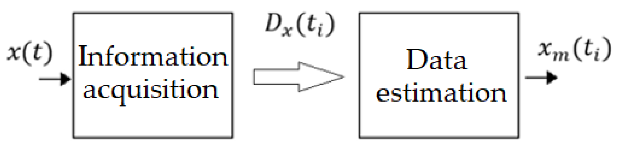
Figure 2.
Structure of the developed device: ADC - analog-to-digital converter; DSM STSL - DSP subsystem module (digital signal processor); FPGA - field programmable gate array; RAM - random access memory; GPP - general purpose processor; USB - universal serial bus; LCD - graphic display.
Figure 2.
Structure of the developed device: ADC - analog-to-digital converter; DSM STSL - DSP subsystem module (digital signal processor); FPGA - field programmable gate array; RAM - random access memory; GPP - general purpose processor; USB - universal serial bus; LCD - graphic display.
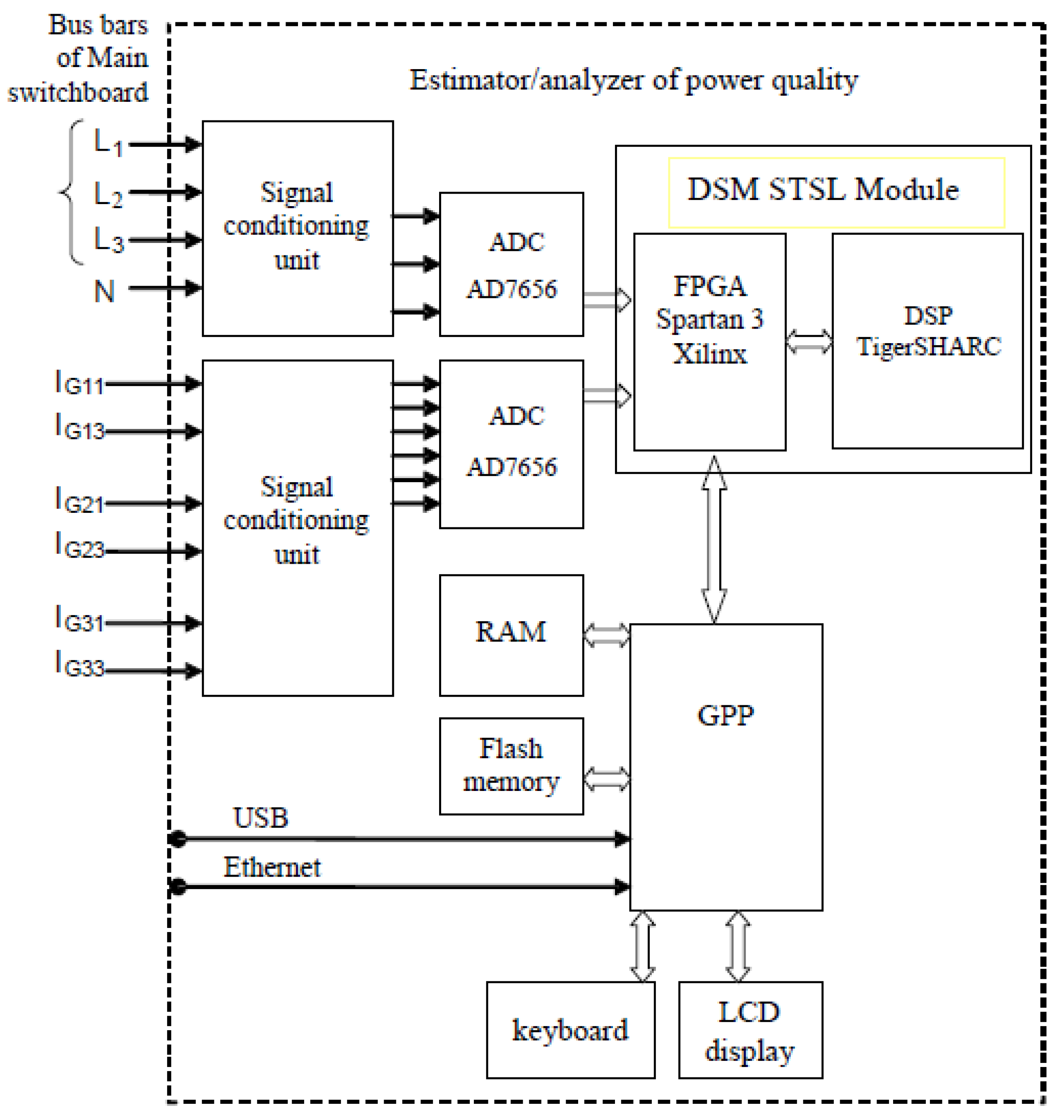
Figure 3.
Configuration of the DSM STSL module [11].
Figure 3.
Configuration of the DSM STSL module [11].
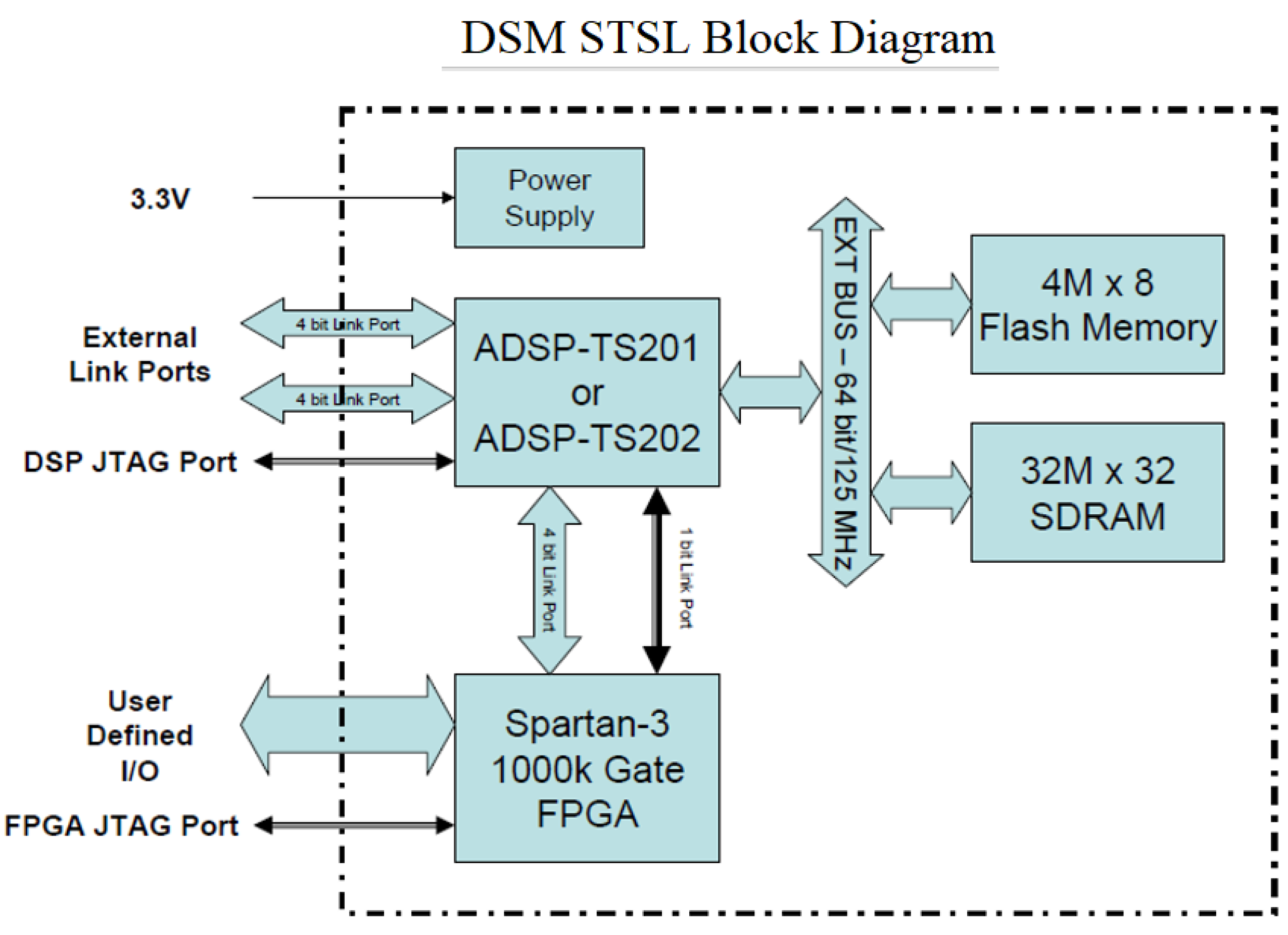
Figure 4.
Configuration of signal conditioning circuits in the device’s voltage channels; input terminals - enable connection of voltages from 3- and 4-wire networks.
Figure 4.
Configuration of signal conditioning circuits in the device’s voltage channels; input terminals - enable connection of voltages from 3- and 4-wire networks.
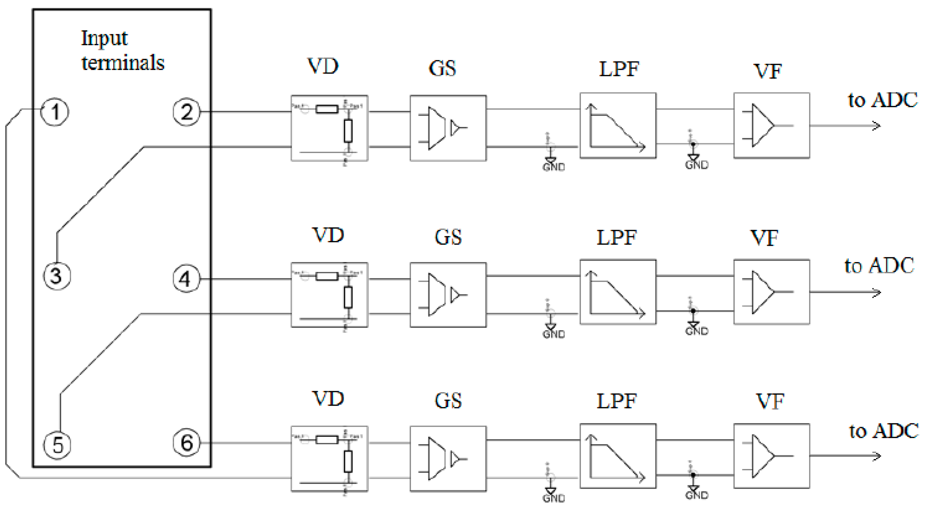
Figure 5.
Signals in the LVDS interface lines; VOD – LVDS peak-to-peak signal, Vcm – common mode voltage [13,14].
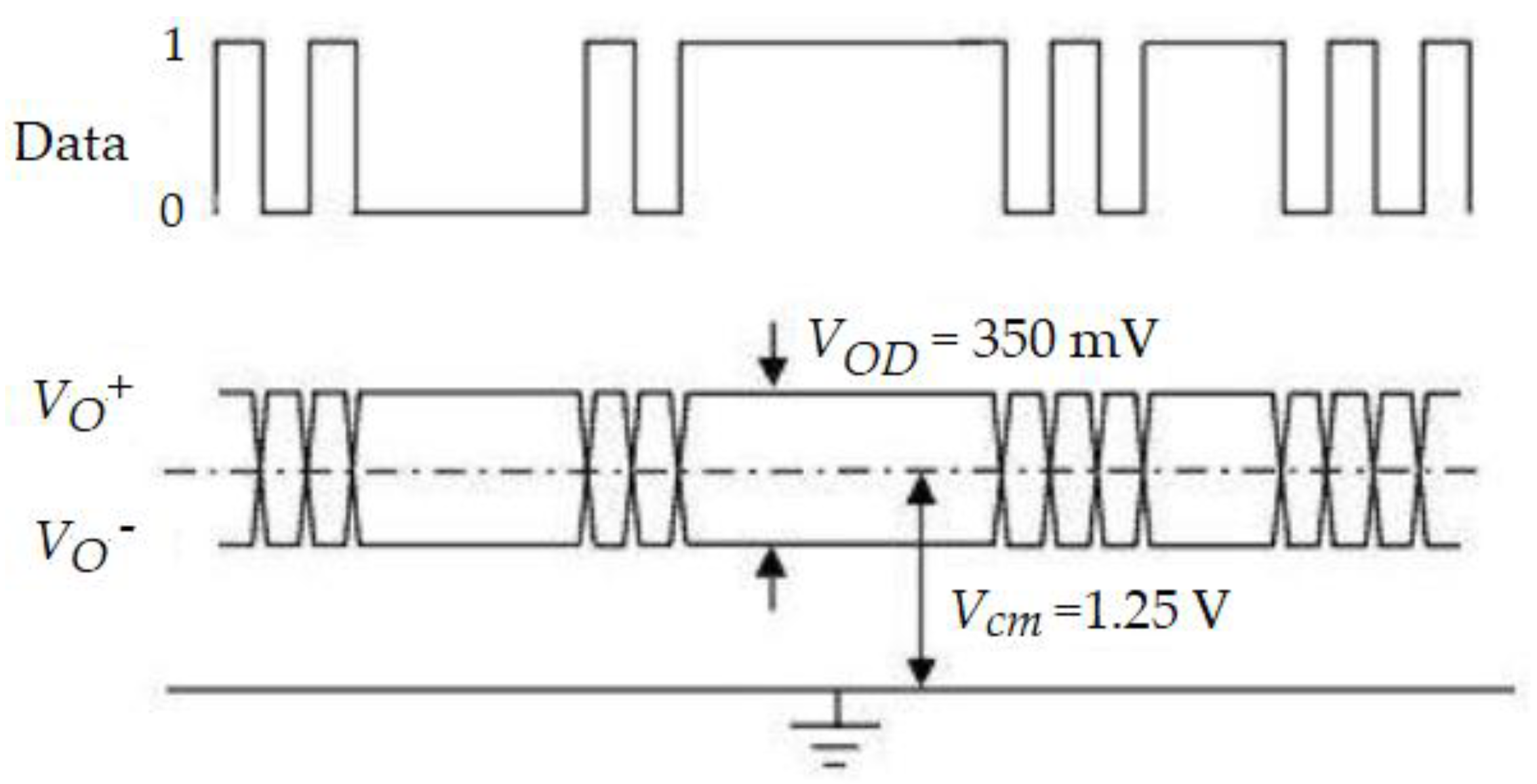
Figure 6.
Timing diagrams on the SPI port lines.
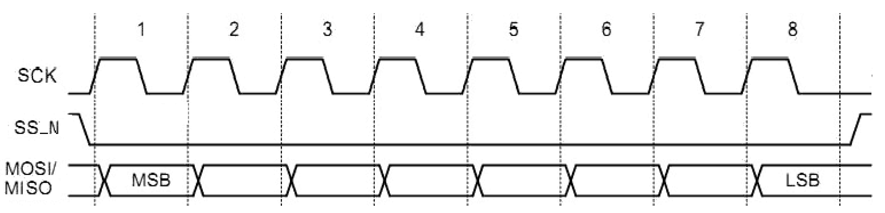
Figure 7.
Device configuration using FPGA to coordinate operations and data conversion between ports of the main device systems: ADC, DSP and GPP [19].
Figure 7.
Device configuration using FPGA to coordinate operations and data conversion between ports of the main device systems: ADC, DSP and GPP [19].
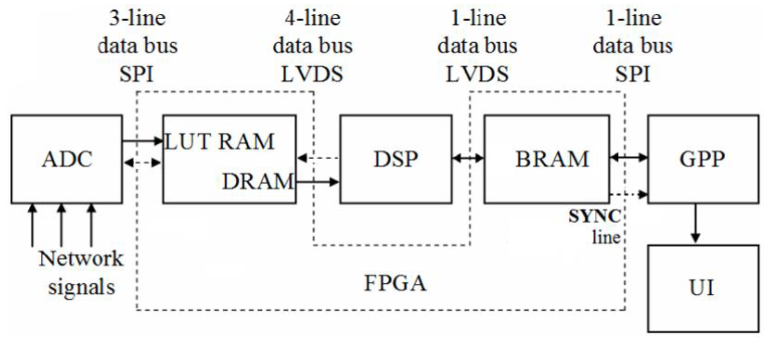
Figure 8.
The idea of data conversion between Link Port and SPI interfaces [16].
Figure 8.
The idea of data conversion between Link Port and SPI interfaces [16].
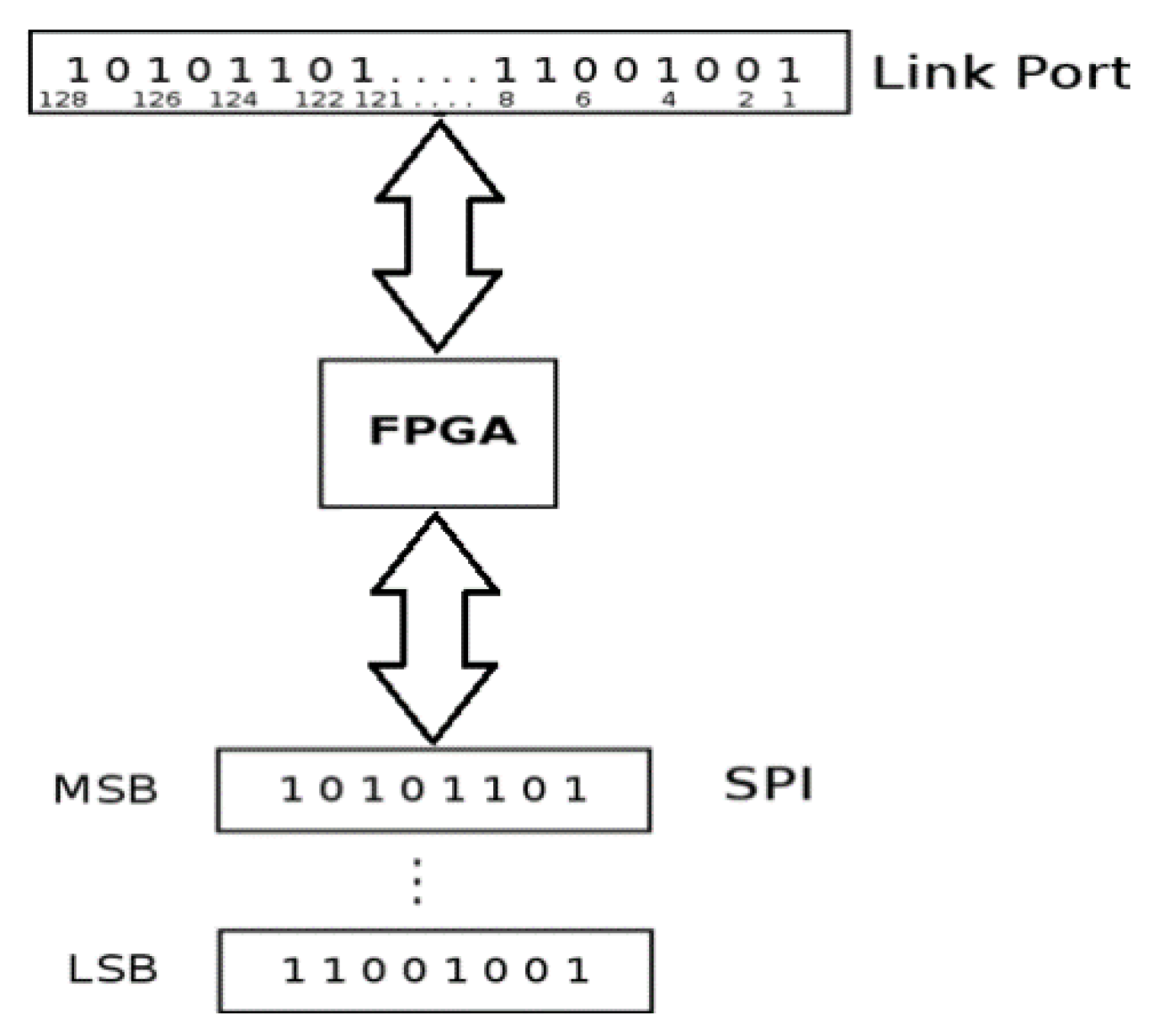
Figure 9.
FPGA configuration for data conversion between Link Port and SPI.
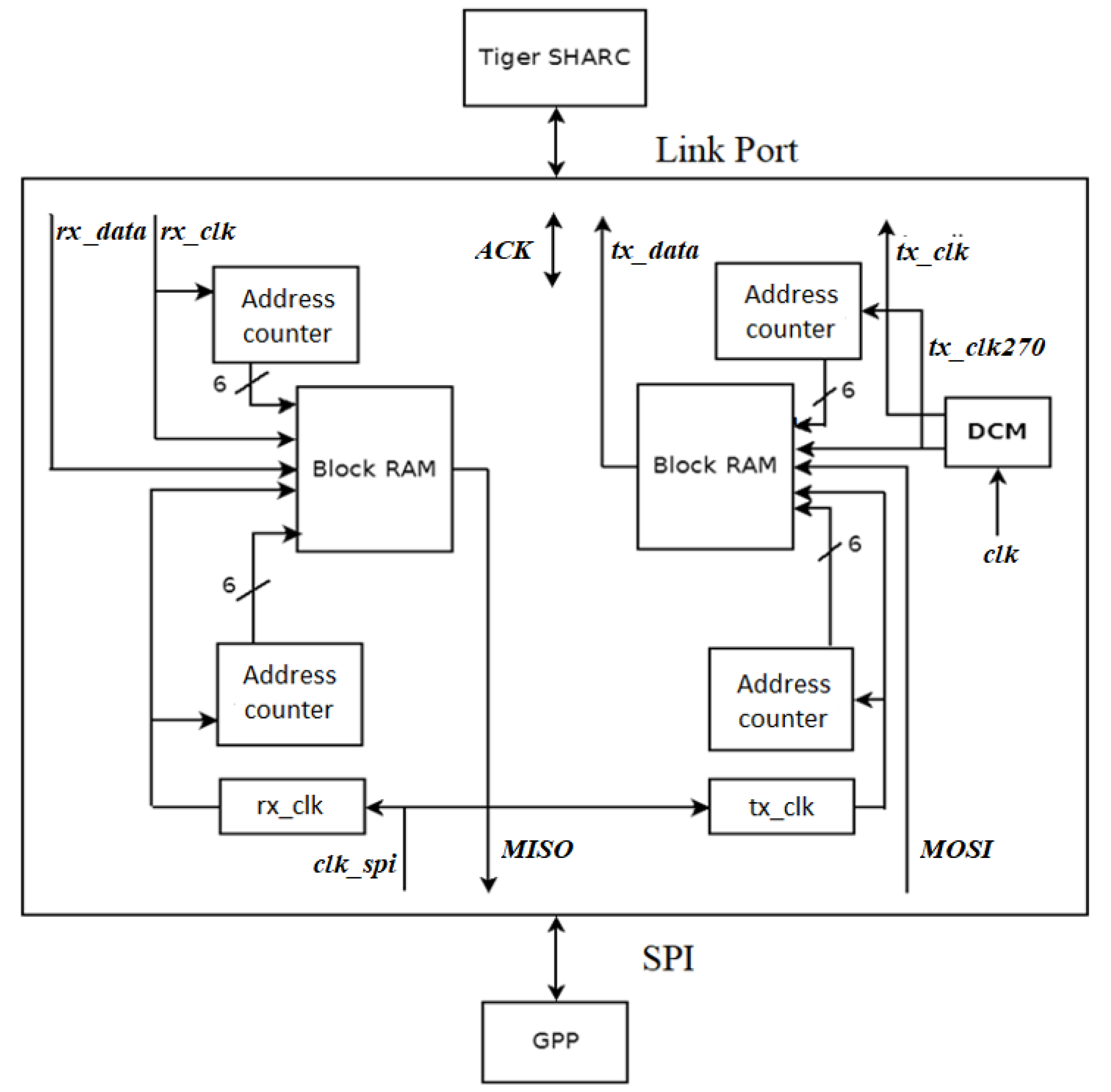
Figure 10.
Functional block diagram of the AD7656 circuit [9].
Figure 10.
Functional block diagram of the AD7656 circuit [9].
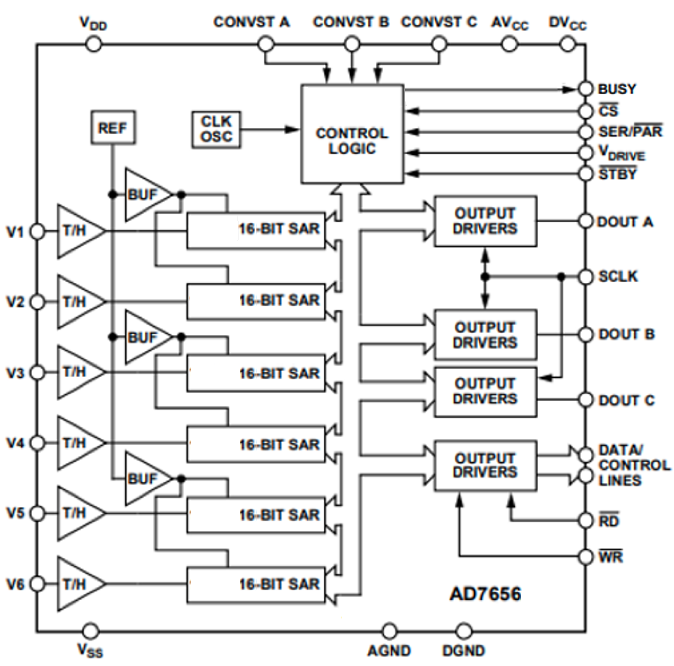
Figure 11.
Data sequence from channels V1- V6 in AD7656 output buffers [9].
Figure 11.
Data sequence from channels V1- V6 in AD7656 output buffers [9].
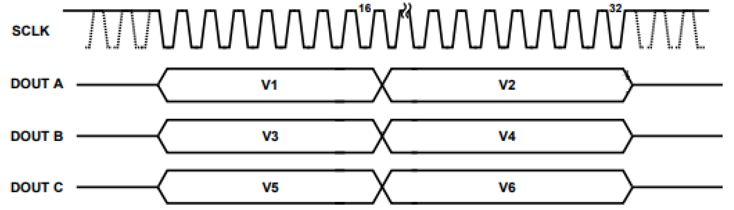
Figure 12.
Algorithm for acquisition of signal samples from the power system and data transfer in the device [26].
Figure 12.
Algorithm for acquisition of signal samples from the power system and data transfer in the device [26].
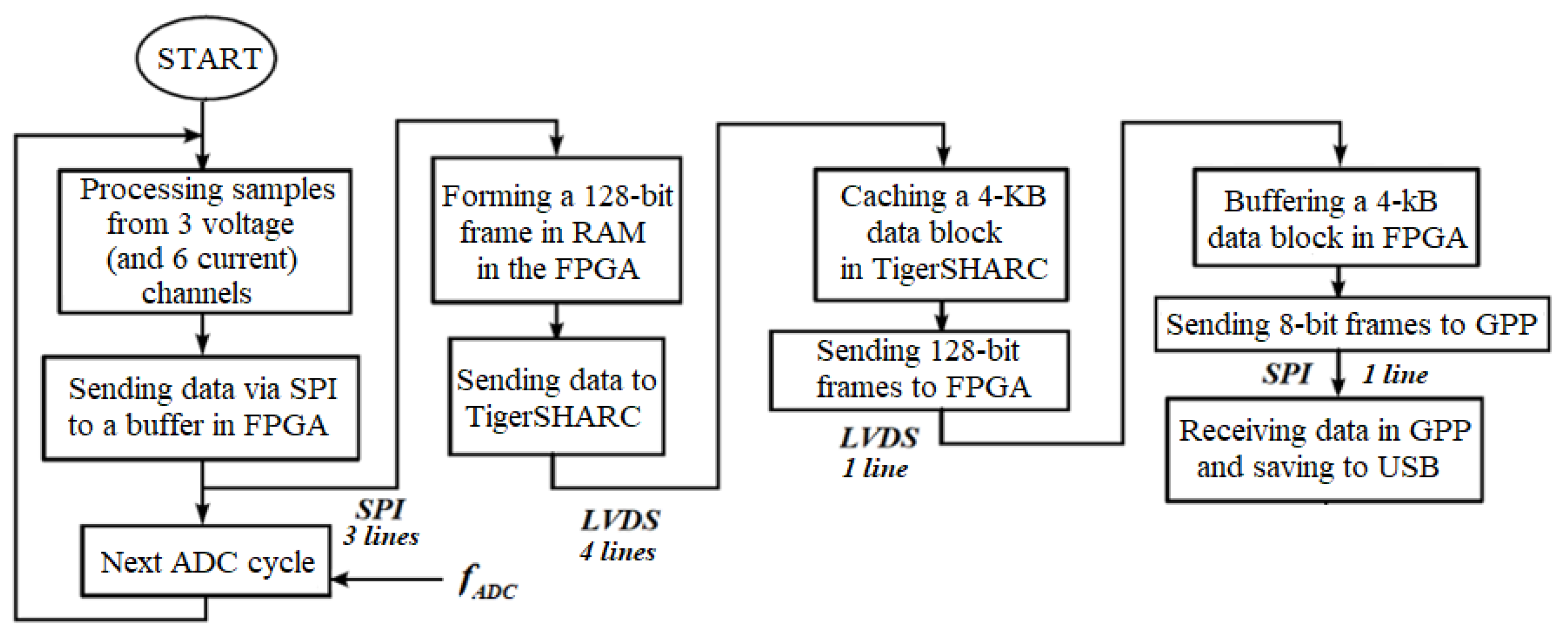
Figure 13.
Managing data transfer to DRAM memory.
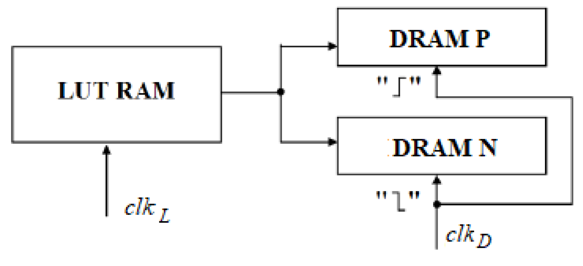
Figure 14.
Bit layout in buffers: (a) ADC; (b) LUT RAM.
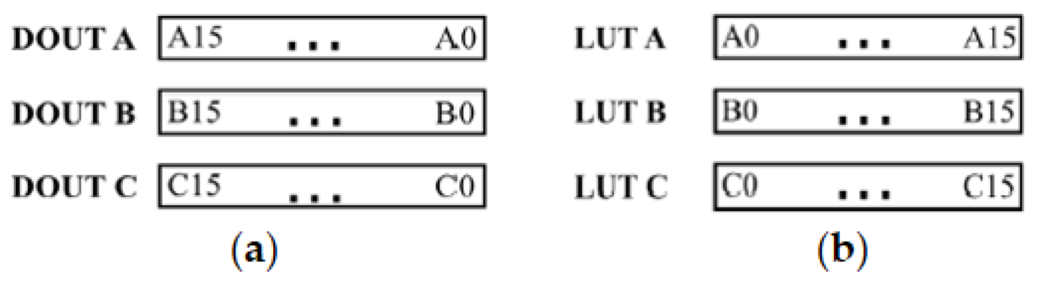
Figure 15.
Data set layout in DRAM in FPGA [19].
Figure 15.
Data set layout in DRAM in FPGA [19].
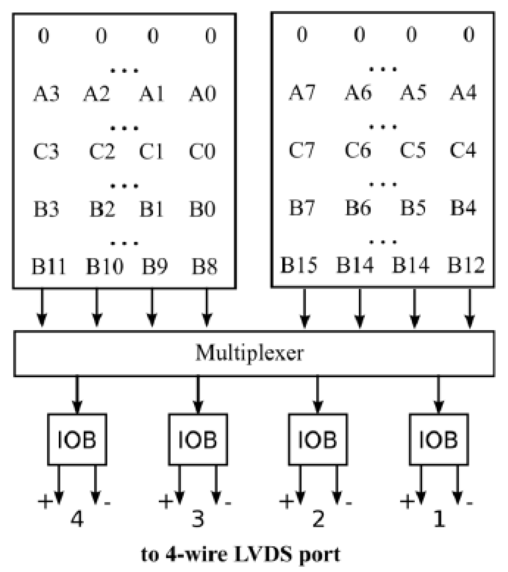
Figure 16.
Time relations in the data recording path, from conversion in the ADC to recording in the DSP buffer [21].
Figure 16.
Time relations in the data recording path, from conversion in the ADC to recording in the DSP buffer [21].
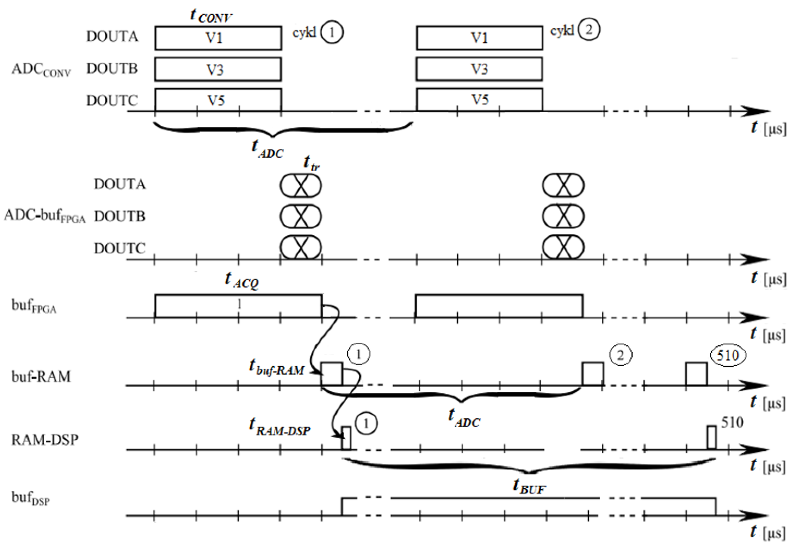
Figure 17.
Time relations of the procedures for sending data from DSP to GPP and saving it on a flash drive.
Figure 17.
Time relations of the procedures for sending data from DSP to GPP and saving it on a flash drive.
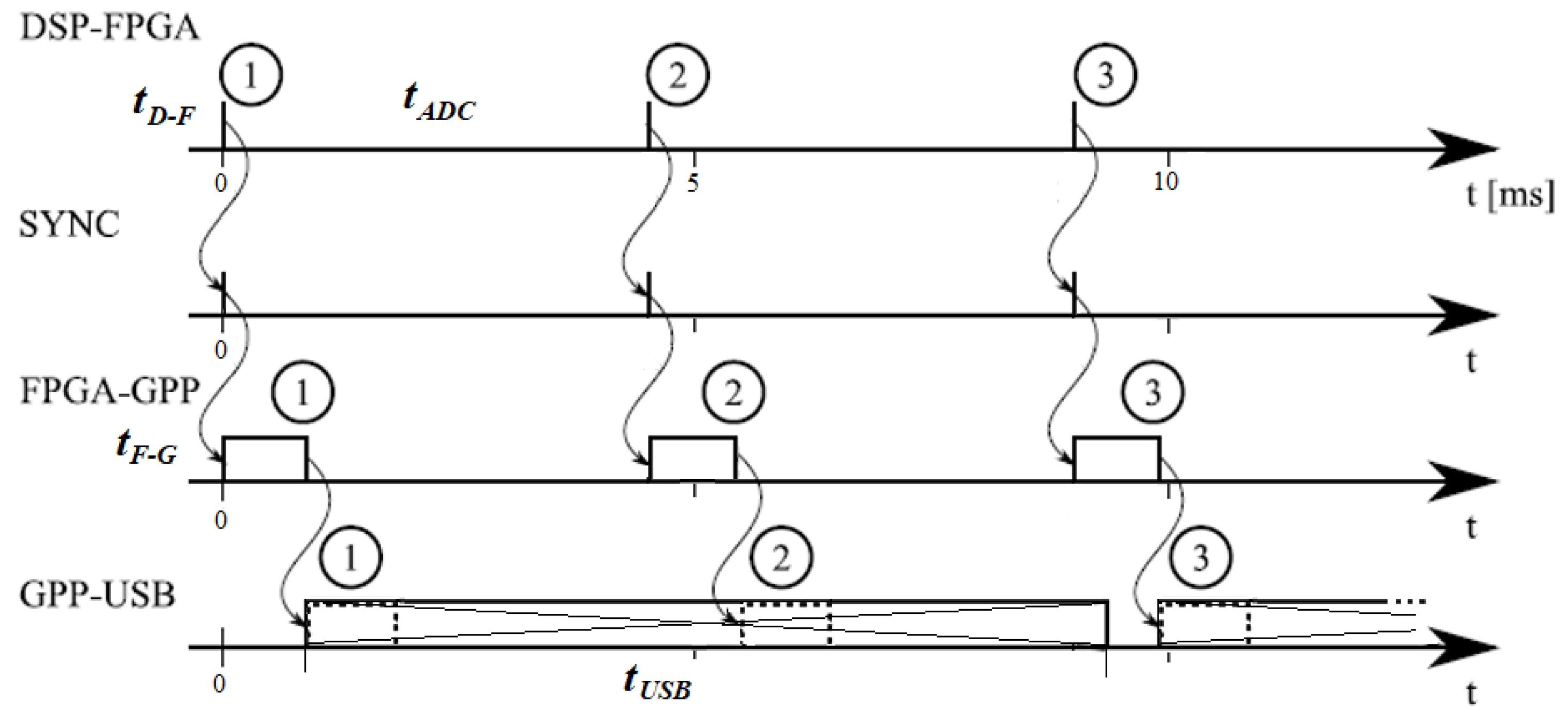
Figure 18.
Methods of coordinating operations in the blocks of the digital measurement chain: (a) central, (b) distributed.
Figure 18.
Methods of coordinating operations in the blocks of the digital measurement chain: (a) central, (b) distributed.
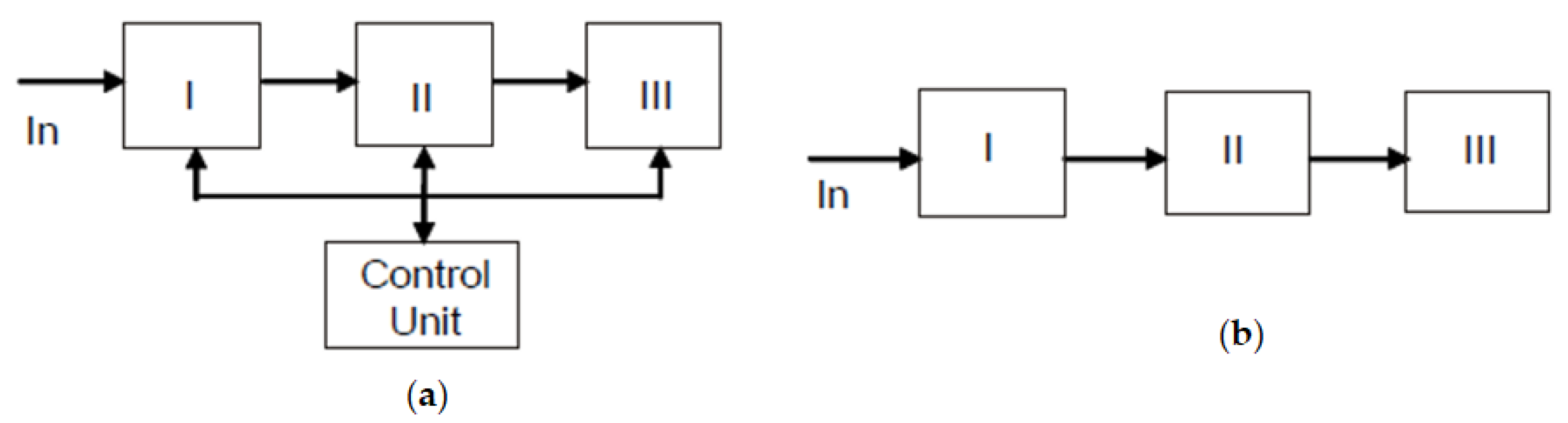
Figure 19.
Time coordination of operations.
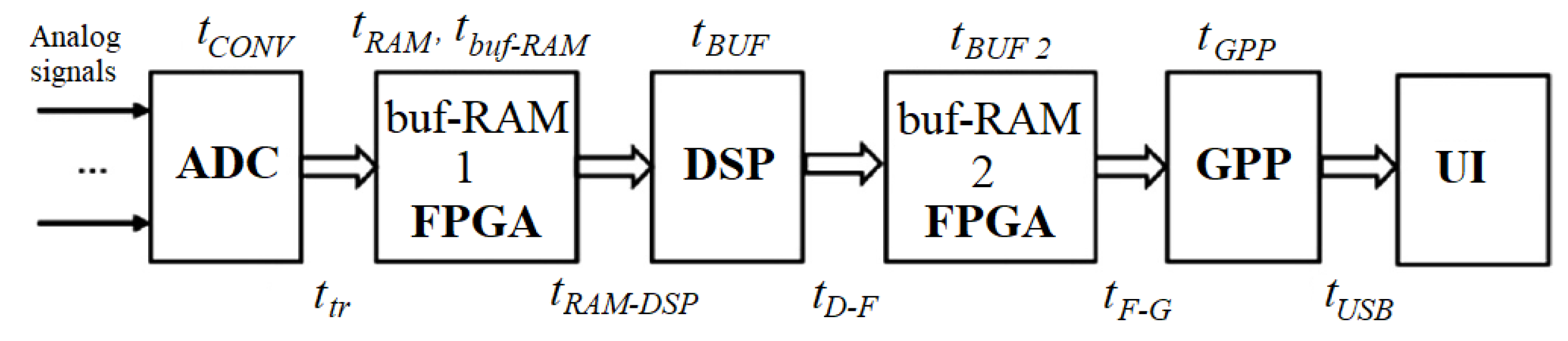
Figure 20.
Simplified block diagram of the measurement track.
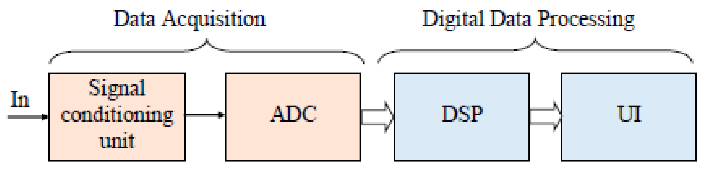
Figure 21.
Calibration protocol for current probe no. 1 [20].
Figure 21.
Calibration protocol for current probe no. 1 [20].
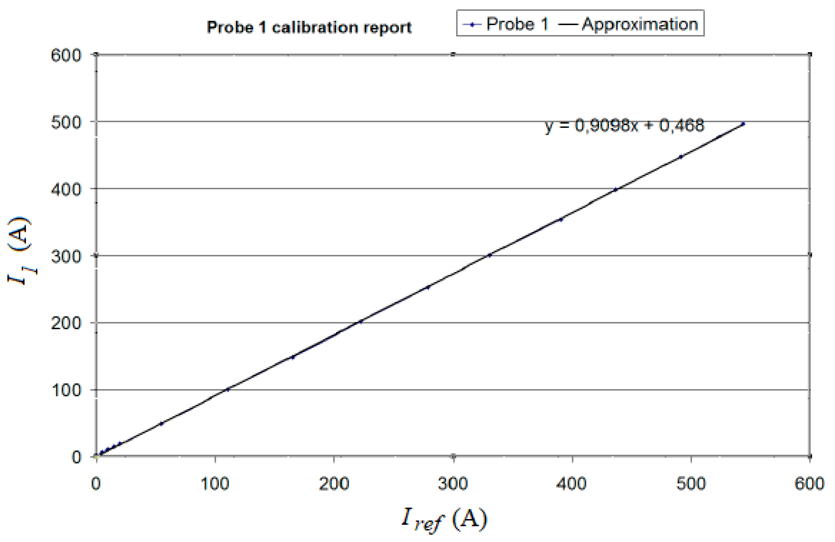
Figure 22.
Deviation between the trend line and the characteristic of current probe no. 1 [20].
Figure 22.
Deviation between the trend line and the characteristic of current probe no. 1 [20].
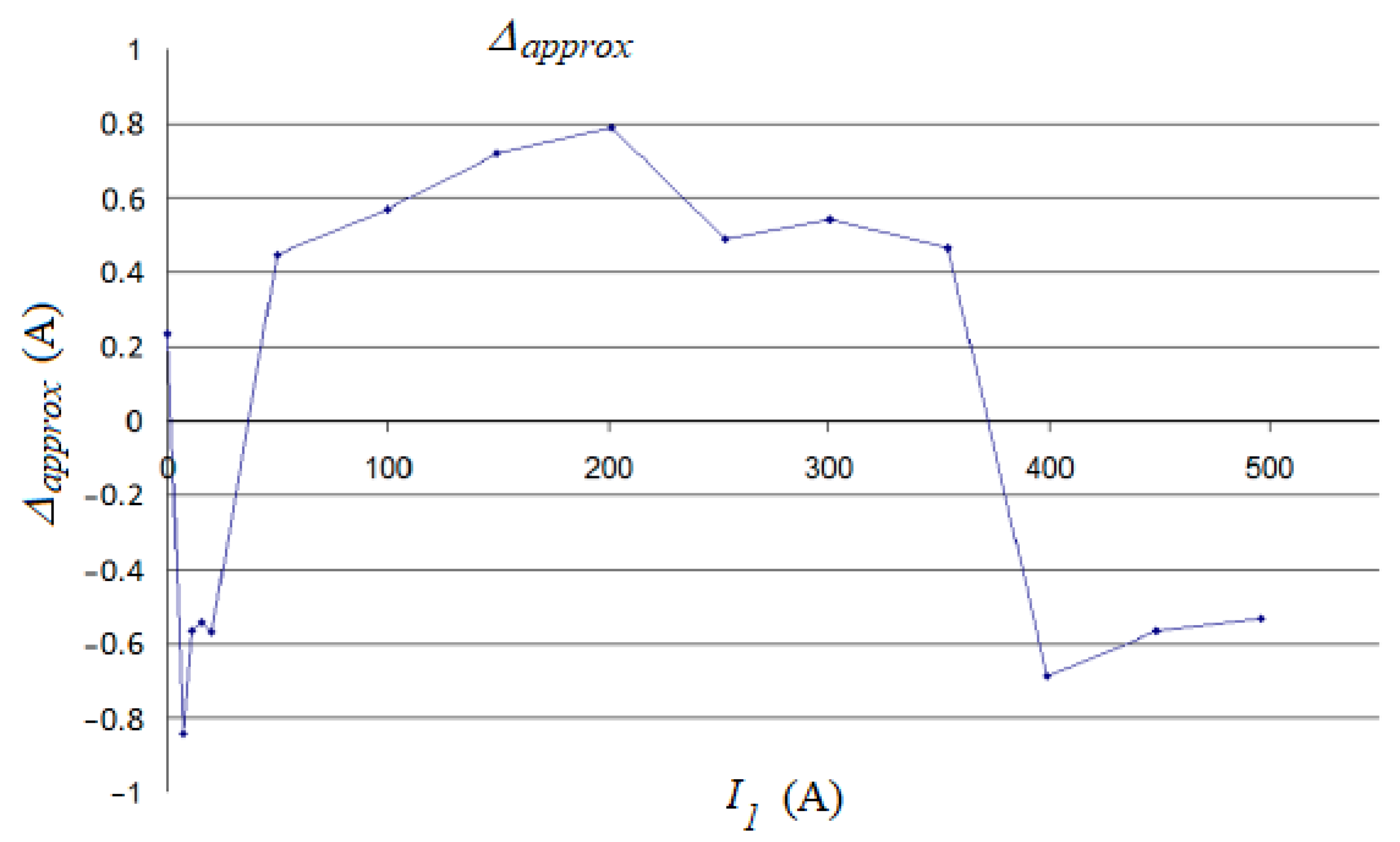
Figure 23.
Measurement track auto-calibration procedures [20].
Figure 23.
Measurement track auto-calibration procedures [20].
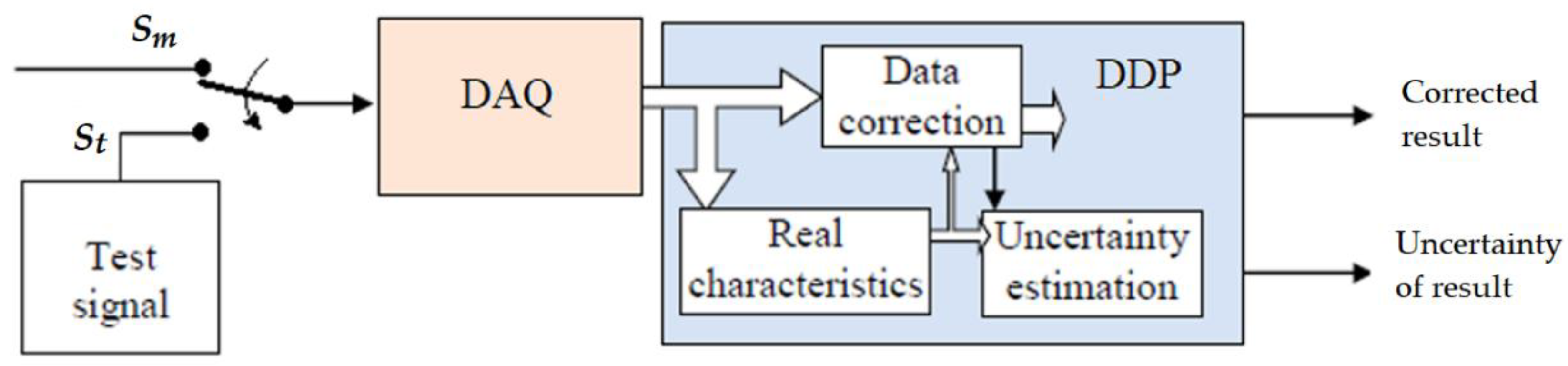
Figure 24.
Diagram of operations performed in software algorithms [20].
Figure 24.
Diagram of operations performed in software algorithms [20].
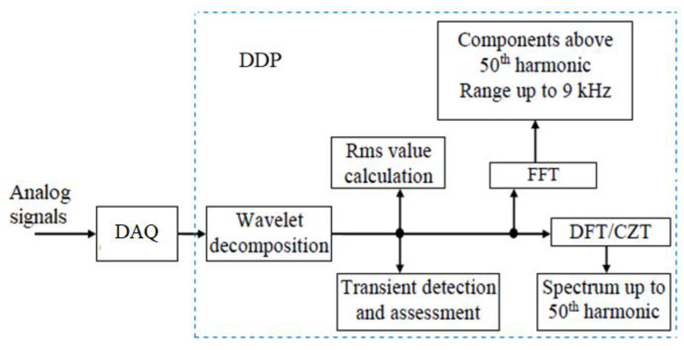
Figure 25.
Systems for assessing the accuracy of the device’s measurement paths: (a) configuration for initial evaluation of algorithms using the start-up kit; (b) evaluation of algorithms using standard analog signals; (c) evaluation of algorithms using raw signal samples and based on the coefficients determined in the device; (d) evaluation using a reference device.
Figure 25.
Systems for assessing the accuracy of the device’s measurement paths: (a) configuration for initial evaluation of algorithms using the start-up kit; (b) evaluation of algorithms using standard analog signals; (c) evaluation of algorithms using raw signal samples and based on the coefficients determined in the device; (d) evaluation using a reference device.
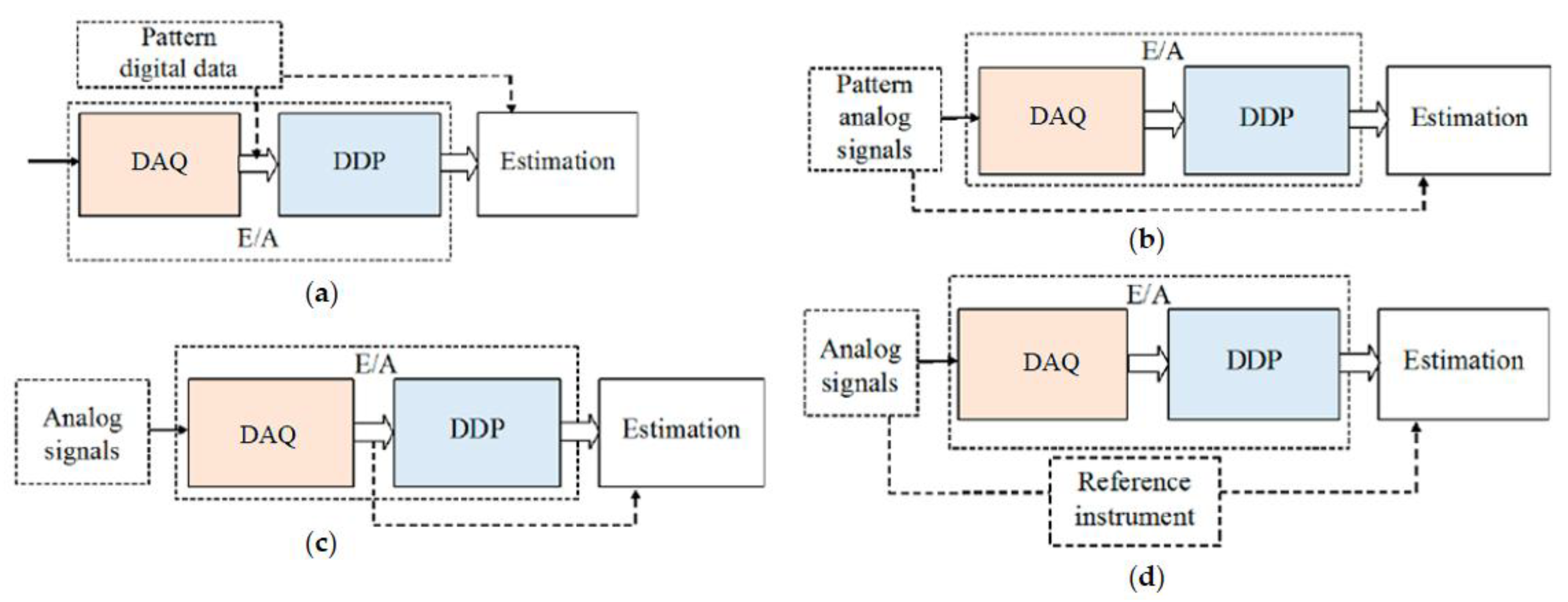
Figure 26.
Validation results of phase voltage measurement channels.
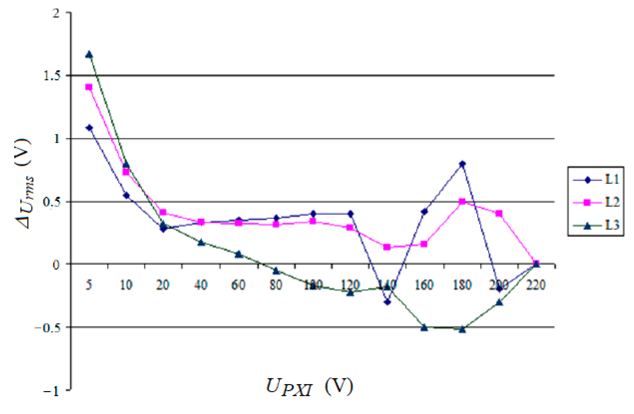
Figure 27.
Verification of measurement algorithms using a set of recorded samples and JEE indices determined on their basis in DSP, after being delivered to the estimation system with a PC.
Figure 27.
Verification of measurement algorithms using a set of recorded samples and JEE indices determined on their basis in DSP, after being delivered to the estimation system with a PC.
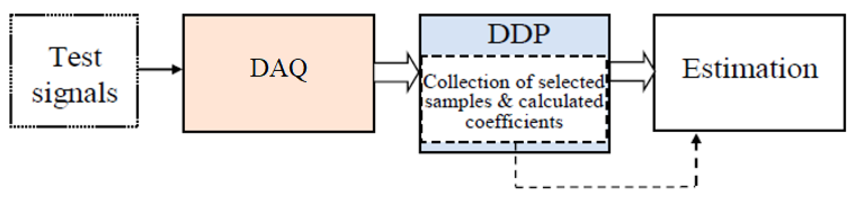

Table 1.
Incorrect writes in USB flash drive memory depending on the time interval between write sessions.
Table 1.
Incorrect writes in USB flash drive memory depending on the time interval between write sessions.
| Frame transmission cycle [ms] |
Bad frames [%] |
| 5 | 0.69 |
| 8 | 0.16 |
| 10 | 0.04 |
| 13 | 0.03 |
| 15 | 0.02 |
| 18 | 0.00 |
| 20 | 0.00 |
| 23 | 0.00 |
Table 2.
Results obtained from the tested device and PC application for the standard DST017 signal from the Chroma programmable AC power source.
Table 2.
Results obtained from the tested device and PC application for the standard DST017 signal from the Chroma programmable AC power source.
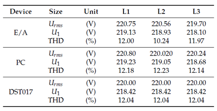
Table 3.
Voltage deviations and their assessment indices in relation to network frequency.
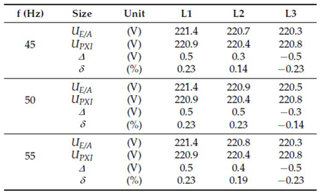
Disclaimer/Publisher’s Note: The statements, opinions and data contained in all publications are solely those of the individual author(s) and contributor(s) and not of MDPI and/or the editor(s). MDPI and/or the editor(s) disclaim responsibility for any injury to people or property resulting from any ideas, methods, instructions or products referred to in the content. |
© 2025 by the authors. Licensee MDPI, Basel, Switzerland. This article is an open access article distributed under the terms and conditions of the Creative Commons Attribution (CC BY) license (http://creativecommons.org/licenses/by/4.0/).
Copyright: This open access article is published under a Creative Commons CC BY 4.0 license, which permit the free download, distribution, and reuse, provided that the author and preprint are cited in any reuse.


