
Submitted:
09 August 2025
Posted:
12 August 2025
You are already at the latest version
Abstract
In order to solve the dynamic adaptation problem of the working frequency band of the FSS in the complex electromagnetic environment and further expand the frequency tuning range, a reconfigurable AFSS unit model based on PIN and varactor diodes are designed, which can achieve the insertion loss below-1 dB in the wide frequency range of 10.2-15.2GHz, meet the working band switching and have the function of flexibly adjusting the working frequency point. In order to verify the accuracy of the design method, a square-ring aperture and notched patch coupling structure that can exhibit broadband transmission response in the X-Ku band is first proposed based on the equivalent circuit model topology. The numerical simulation and processing test of the structure are carried out. The measured data are in good agreement with the simulation results. After optimizing the unit structure, different capacitance values and resistance values are added to the diodes in the numerical simulation to control the equivalent PIN diodes switch and the capacitance change of the varactor diodes. According to the equivalent circuit model and the electric field intensity distribution, the AFSS regulation mechanism of the loaded diodes is explored. In this paper, through numerical simulation optimizations and experimental verification, the design method and performance optimization strategy of frequency- tunable FSS in the working range of 2-18 GHz are systematically studied, which provides theoretical support for the design of electromagnetic functional devices in the new generation of communication, radar and electronic warfare systems.
Keywords:
frequency selective surface
; equivalent circuit method
; reconfigurable
; frequency tuning
; bias feeding
1. Introduction
Frequency Selective Surfaces (FSS) are two-dimensional periodic artificial electromagnetic structures with spatial filtering characteristics. They comprise subwavelength-sized metal patches or aperture units arranged in a specific spatial period [1]. Under ideal condition, FSS reflect or transmit electromagnetic signals within designated frequency bands without absorbing energy. Through optimized structural design, precise regulation of electromagnetic waves can be achieved.
Contemporary military radar antennas and wireless communication systems increasingly demand broadband and frequency-agile operation. Most traditional FSS are designed for fixed frequency bands and struggle to adapt to dynamic requirements in complex electromagnetic environments. To address this, Active Frequency Selective Surfaces (AFSS) integrate electronic control devices into traditional structures. By adjusting external excitation, AFSS dynamically modify electromagnetic performance to achieve reconfigurable characteristics [2,3].Among methods for realizing AFSS reconfigurability [4,5,6], designs incorporating PIN diodes or varactor diodes offer advantages including rapid frequency response, flexible functionality switching, and low fabrication costs, enhancing practicality [7,8,9]. Early work by Ghaffer et al. (2007) [10] loaded PIN diodes onto a single-layer FSS structure, demonstrating electromagnetic property switching via diode on/off control. In 2011, Withayachumnankul. [11] achieved wideband tunable performance (2.7–3.5 GHz) by loading varactor diodes into an AFSS parallel resonant unit. Subsequently, Amir Ebrahimi et al. (2016) [12] proposed a bandpass FSS with variable capacitance tuning, exhibiting nearly constant bandwidth across a 3.7–5.2 GHz tuning range. Li Huangyan (Nanjing University of Aeronautics and Astronautics, 2019) [13] advanced multifunctional AFSS technology, proposing a PIN/varactor-loaded resonant model capable of integrated transmission/reflection switching, polarization selection, and frequency tuning (1.3–2.1 GHz). Later, He Zhangjian (2022) [14] optimized bias network design for miniaturization. The resulting PIN-diode-based reconfigurable AFSS achieved broadband operation and high selectivity, enabling passband/stopband switching (4.2–5 GHz) and frequency tuning (2.17–4.8 GHz), while maintaining stable transmission at incident angles up to 60°.As shown, AFSS resonant frequency, bandwidth, and other electromagnetic properties can be reconfigured by integrating active devices and applying external excitation. However, conventional electronic components typically enable only single-frequency-point tuning within small ranges, while incorporating numerous tuning elements introduces significant insertion loss. A critical challenge persists in AFSS technology: ensuring stable transmission responses while achieving wide-range frequency reconfigurability via integration of extensive active devices.
This paper integrates theoretical analysis, simulation modeling, and experimental validation. Firstly, a unit cell topology based on a second-order circuit model is established. The feasibility of subsequent active frequency-selective surface (AFSS) design is verified by comparing numerical simulations with experimental measurements. Secondly, an optimized reconfigurable unit cell is developed by integrating PIN diodes and varactor diodes, alongside a rationally designed bias network to minimize additional insertion loss. This structure achieves passband tuning with insertion loss better than -1 dB across 10.2–15.2 GHz through capacitor adjustment and switch control. Switching between two operational bands (X-band to Ku-band) is realized by toggling the PIN diode states, while continuous frequency tuning within each band is enabled by adjusting the varactor diode bias voltage. The operating mechanism of the AFSS is elucidated through equivalent circuit modeling and electric field distribution analysis, providing valuable insights for flexible frequency control in AFSS technology.
2. Verification of Design Principles and Methods
2.1. Equivalent Circuit Method
In the study of periodic FSS array structures, the equivalent circuit method (ECM) provides an efficient and intuitive approximation. Based on quasi-static electromagnetic field assumptions, ECM models the FSS unit cell as a lumped-parameter circuit equivalent to a transmission line model [15,16]. This study employs ECM to develop the basic unit cell topology, enabling rapid calculation of FSS resonant characteristics from equivalent circuit parameters.
As shown in Figure 2.1, for a square ring aperture array, when the gap of the aperture is much smaller than the size of the periodic element, the square ring aperture can be equivalent to an LC parallel circuit, and its equivalent circuit impedance satisfies Equation (2.1):
The deformation of equation (2.1) yields the circuit impedance that satisfies:
When the impedance in Equation (2.2) tends to infinity, the resonant frequency satisfies:
According to circuit theory, when the input frequency equals the resonant frequency, the inductive and capacitive impedances balance each other. At resonance, the equivalent impedance becomes theoretically infinite, and currents through the inductor and capacitor exhibit equal magnitude but opposite phase. Consequently, the AC signal cannot shunt to ground through the LC parallel circuit. Under this condition, the square ring aperture array (FSS) exhibits bandpass characteristics at the resonant frequency.
In order to clarify the relationship between structural dimensions and equivalent capacitance, inductance, empirical formulas for calculating these parameters have been developed. The following approximations provide relatively accurate equivalent inductance (L) and capacitance (C) values for surface-mounted metallic unit cells [17]:
The meanings of each parameter are shown in Figure 2.1(a) above, where, , and are the length, width and gap interval of the metal strip respectively, is the effective dielectric constant of the dielectric layer; is the dielectric constant in vacuum; is the magnetic permeability in vacuum.
An LC parallel circuit typically provides only one bandpass resonance point. According to filter theory, while first-order filter models feature simple structures, they exhibit wide transition bands and insufficient stopband attenuation, leading to poor filtering performance [18]. In order to enhance the frequency selection characteristics of FSS, it is considered to cascade multiple parallel LC resonant models to achieve high-order filtering responses [19,20]. This section adopts a second-order filtering model, corresponding to a double-layer metal patch cascade structure for FSS. As shown in Figure 2.2, the equivalent circuit model of the second-order filter structure is presented. The aperture structures loaded on both sides can be respectively equivalent to L1C1 and L2C2 parallel circuits, and the dielectric substrate is regarded as a transmission line with a certain characteristic impedance, which can be equivalent to a parallel capacitor Cr and a series inductor Lr.
2.2. Structural Design and Numerical Simulation Research
The structural topology is applied to the equivalent circuit model in Figure 2.2. Compared to other unit types, the annular structure suppresses premature excitation of higher-order harmonics while demonstrating superior frequency response stability. Consequently, a novel structure featuring coupled square-ring apertures and notched patches is designed, based on a conventional square-ring unit. Figure 2.3 presents the designed unit structure model. The specific structural dimensions after optimization are shown in Table 2.1, and the medium substrate material selected is TLY-5.
Numerical simulations of the initial structure were performed using CST Studio Suite 2018. Figure 2.4 shows the transmission and reflection coefficients under normal TE-polarized wave incidence. Mutual coupling between the dual-layer resonators expands the bandwidth and sharpens the roll-off characteristics. The -1.5 dB bandwidth measures 5.4 GHz (7.4–12.8 GHz), corresponding to a 53.5% fractional bandwidth. This structure exhibits excellent in-band performance with low insertion loss and high transmission efficiency, while the stopband demonstrates a flat reflection coefficient profile and strong out-of-band suppression.
For numerical modeling, electromagnetic simulations were primarily performed using CST Studio Suite (based on the Finite-Difference Time-Domain method). Complementary verification employed ADS (Advanced Design System) implementing the Equivalent Circuit Method (ECM). The equivalent circuit model in Figure 2.2 was implemented in ADS to compute S-parameters. Figure 2.5 compares simulated results from CST and ADS. For analytical clarity, only the reflection coefficient (S₁₁) is shown.
Comparative analysis reveals close agreement between the reflection coefficient curves obtained from both software simulations, with strong correlation in overall results. Minor discrepancies occur at the second resonant frequency due to electromagnetic coupling effects between unit cells and layers in the FSS structure – a phenomenon not captured in the equivalent circuit model optimization. Although slight parameter variations exist between circuit-optimized and full-wave-optimized values, the equivalent circuit method remains effective for rapid FSS design iteration.
2.3. Angular Stability Validation
In this paper, numerical calculations were also conducted on the frequency response curves when different angles were incident on the FSS. The results are shown in Figure 2.6. In the TE polarization mode, as the incident angle increases, a certain shift occurs at the high-frequency cut-off point. However, overall, this broadband FSS structure still maintains good angular stability within the range of 0° to 45°.
2.4. Experimental Testing and Data Analysis
This FSS sample adopts the precision etching process. The processing model and dimensions are completely in accordance with the size parameters in Table 2.1. The processed sample is shown in Figure 2.7. The physical size of the entire sample is 202mm*202mm, and the medium plate is made of TLY-5 material.
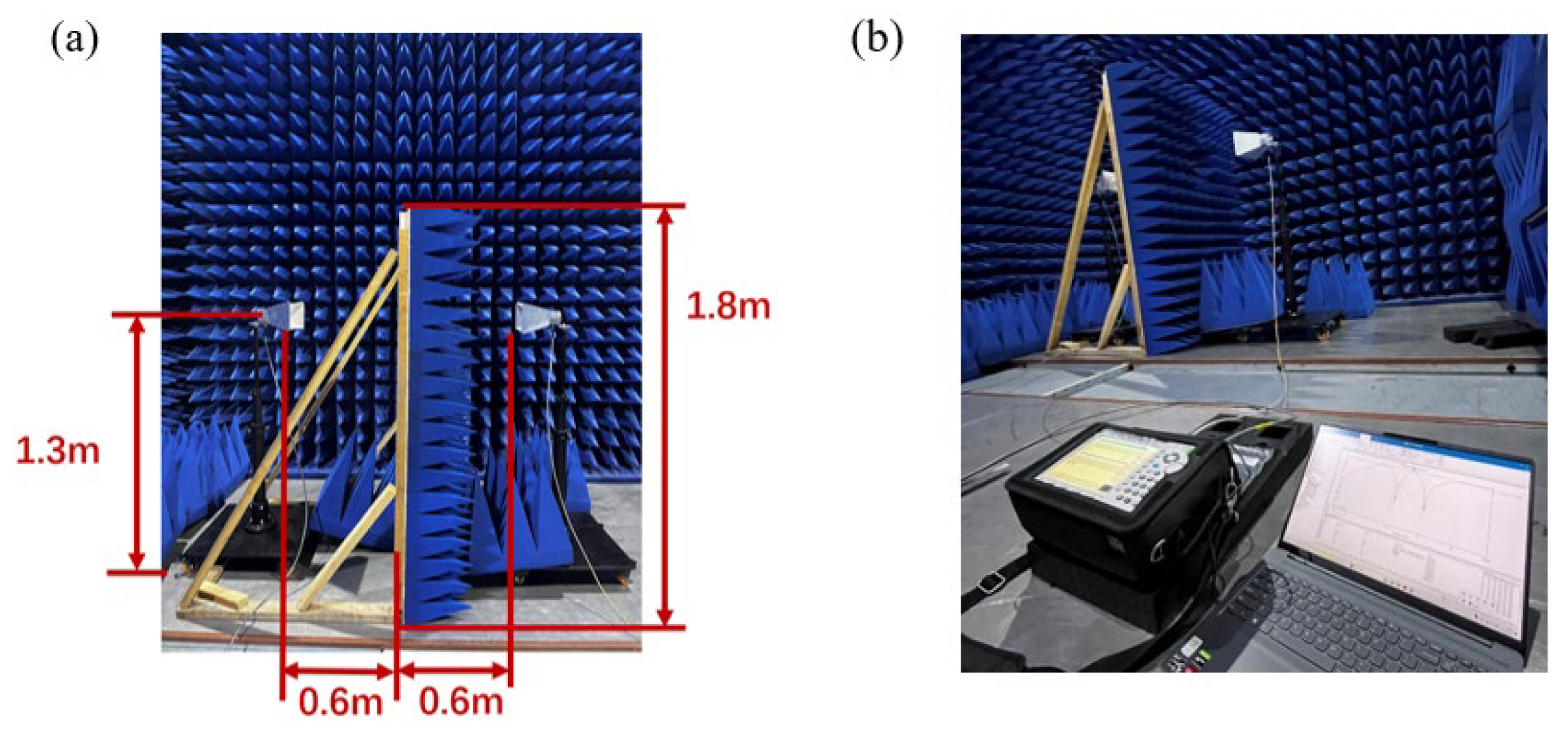
The entire experimental test was carried out in a microwave anechoic chamber, and the free-space method was selected for the test. The operating frequency band of the horn antenna is 1-18 GHZ. The two ports of the vector net meter are respectively connected to the transmitting antenna and the receiving antenna. Preheating and equipment calibration are required before each test.
Figure 2.8.
Test system setup environment(a)Physical picture of the test device(b)Physical connection picture of the arrow net instrument.
Figure 2.8.
Test system setup environment(a)Physical picture of the test device(b)Physical connection picture of the arrow net instrument.
After calibration, the test piece was placed for testing. Figure 2.9 shows the comparison between the measured results and the simulation results when the electromagnetic wave is vertically incident in the TE polarization mode. At the reflection curve, the measured amplitude at 8.5 GHz is -41.2 dB, and the insertion loss during simulation is -30.5 dB. At the wideband depression (11.1 GHz), the amplitude of the reflection coefficient curve in simulation calculation is -5.4 dB, while the actual test shows -9.8 dB. The measured insertion loss is less than that during simulation. There is no significant deviation between the passband width and the resonant center frequency, and the results are basically consistent.
The FSS performance test was also conducted on the sample when electromagnetic waves were incident at an Angle. Due to the limited conditions in the actual test, it was impossible to precisely rotate the turntable that fixed the sample to be tested at an Angle. Therefore, we only tested the case when the incident Angle was 15°. Figure 2.10 shows the comparison of the actual test and simulation results of the reflection coefficient and transmission coefficient curves in the TE polarization mode.
It can be seen that the resonant frequency points of the reflection coefficient and transmission coefficient curves hardly shift. The 15° oblique incident is in good agreement with the simulation results. However, stray waves occur in the higher frequency band of 12.9 GHz. In the actual test, the amplitude at the passband decreases by about -10 dB on average, and the insertion loss is significantly less than the simulation results.
Analyze the error of the difference in insertion loss of the reflection coefficient in the experiment: In an ideal situation, FSS assumes that there is no material loss, the structure is perfectly symmetrical, and there are no other energy loss mechanisms. When the impedance is fully matched, the relationship between the transmission coefficient () and the reflection coefficient () can be expressed by the formula ||²+||²=1, where the square modulus of and represents the transmittance and reflectance respectively. In simulation, electromagnetic waves are only transmitted or reflected. However, in the actual test environment, some electromagnetic waves will be lost in the air or absorbed by absorbing materials during transmission, resulting in ||²+||²<1. Therefore, the reflection coefficient calculated based on the transmission coefficient in the actual environment must be smaller than that in the ideal environment.
In summary, by comparing the transmission curves of the measured results with those of the simulation results, it is found that there is no significant deviation in the passband width and the resonant center frequency, and the error is within a reasonable range. Based on the calculation results of the two numerical simulations of ADS and CST in Figure 2.5 above, the accuracy of the entire model design was verified. This provides an accurate design basis for the subsequent AFSS active reconfigurable model design.
3. Research on the Structural Model Design and Regulation Mechanism of AFSS
In order to achieve AFSS with band switching function and frequency tuning characteristics, it is proposed to adopt the fusion loading method of switching devices and varactor diodes. In addition, the feeding of diodes is all through the upper and lower layer structure and the metal through holes to form a fusion bias network. A simple metal bias network model is used to provide feeding for AFSS to achieve bias voltage regulation.
3.1. Resonant Structure Design
According to the analysis in Section 2.4, it can be known that the annular structure has good polarization and incident angle stability, and has a stronger inhibitory force on the grid flap. Therefore, the square ring structure is tortuous and transformed. The aperture unit and the central patch are two nested parts inside and outside, insulated from each other to facilitate power supply to the active device. The bent structure extends the length of the metal band grid and the aperture, increasing the equivalent inductance and capacitance to a greater extent. Secondly, the bent structure is conducive to the realization of miniaturization, which has a significant advantage in improving the stability of the incident Angle [21].
For the biased network design, it is also proposed to bend the cross-cell structure. Figure 3.1(a), (b), and (c) show the evolution process of the cross bending. Simulations were conducted on the FSS combined structure with a ring structure loaded on the top layer and three types of cross patch units loaded on the bottom layer respectively. The S-parameters under different oblique Angle incident conditions are shown in Figure 3.1(d), (e), and (f).
It can be seen that as the degree of miniaturization increases, the continuous increase in the number of bends causes the resonant frequency to shift towards the low frequency, and the resonant bandwidth gradually Narrows. The relative bandwidth of the unbent cross patch is 23.6% (13.8 GHz-10.8 GHz), while that of the double-bent cross patch structure drops to 7.4% (11.1 GHz-10.3 GHz). After three bends, the relative bandwidth of the cross-shaped patch drops to 6.7% (9.4 GHz-10.0 GHz). In the unbent cross structure, a frequency offset of 0.3 GHz occurs when the incident is normal and the incident is oblique at 45°. The frequency hardly shifts during the secondary bending, but the bandwidth decreases when the incident is oblique compared to the normal incident. After three bends, the resonant frequency and working bandwidth of the structure remain almost unchanged when the incident is oblique. This indicates that the more bends are introduced into the branch, the greater the angular stability will be.
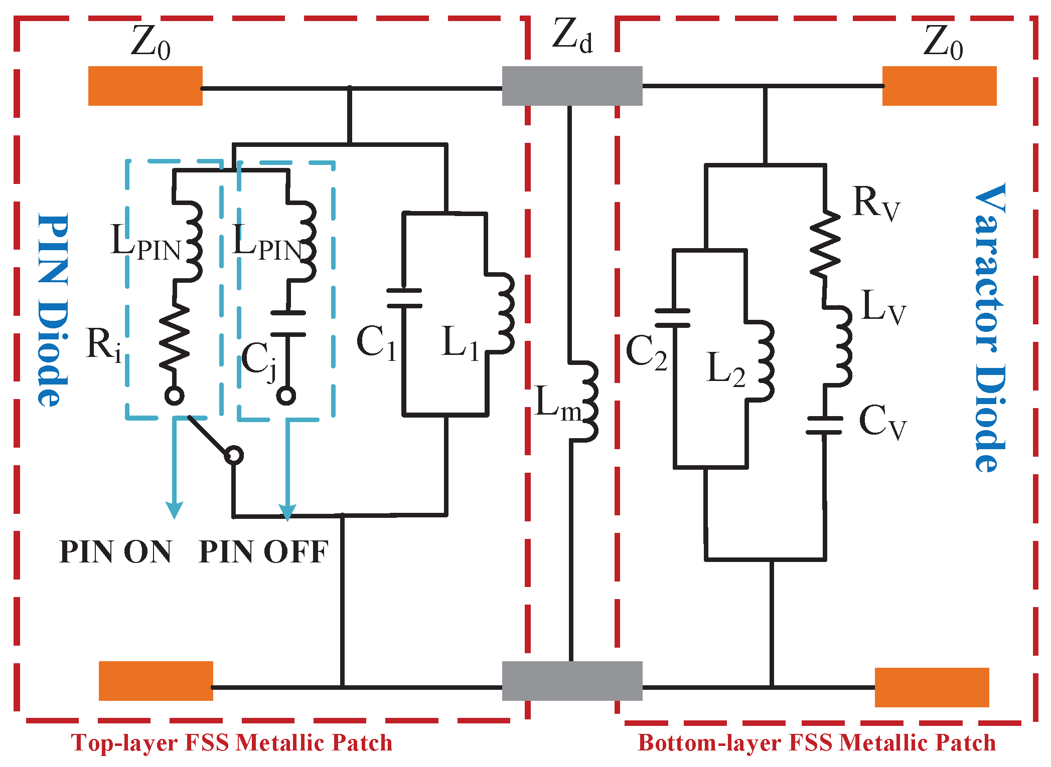
The feeding mode of the active structure considers placing four diodes (two PIN diodes and two varactor diodes) symmetrically along the Y-axis direction in the unit structure. The anodes of all diodes are connected to the metal part inside the annular hole diameter, and the cathodes are uniformly connected to the outer conductor to form a circuit. In this design, the cross-shaped surface mount is placed in the middle layer. The metal through hole at the center of the unit serves as the feed network for this active structure model, providing a bias voltage for the diode [14].
3.2. Analysis of Passive Structure Model and Transmission Characteristics
3.2.1. Structural Model Design
After completing the design optimization, the AFSS structure model of the fusion loading diode proposed in this project is shown in Figure 3.2 (a). The overall model consists of three metal layers and two dielectric substrates spaced apart. The top and bottom metal layers are made of traditional square ring hole diameter structures that have been deformed and have exactly the same structural dimensions. The middle power supply layer is a tortuous structure formed by bending a traditional cross patch with branches to enhance the angular stability of the overall structure. The medium material selected is Rogers 5880. Metal through holes run through the entire structure for convenient power supply. Other parameters of the structure are shown in Table 3.1:
The numerical simulation results of the positive incident electromagnetic waves in the TE polarization mode are shown in Figure 3.3. At this point, the bandpass resonance point of the S-parameter curve is 12.2 GHz, and the -3dB operating bandwidth is 1.8 GHz(11.4-13.2 GHz).
Meanwhile, the working characteristics of the structure when electromagnetic waves are incident obliquely were investigated. As shown in Figure 3.4, in the TE polarization mode, when the oblique incident Angle increases from 0° to 45°, the passband only shifts slightly: The resonant center frequency slightly shifts from 12.2GHz to the low frequency of 12.1 GHz, and the -3 dB bandwidth decreases from 1.8 GHz(11.4 GHz-13.2 GHz) to 1.5 GHz(12.9 GHz-11.4 GHz) and 1.1 GHz(12.6 GHz-11.5 GHz), respectively. Although the increase in the oblique incident Angle brings about a certain degree of high-order resonance at higher frequency points, the operating frequency point remains almost unchanged, and good bandpass characteristics can still be maintained in the operating band. This stability is brought about by the low profile of the structure and the miniaturization design of the bending structure.
When the oblique incident angle increases from 0° to 60°, the resonant frequency slightly shifts to the low frequency by 0.4 GHz, and the bandwidth at -3dB decreases from 1.8 GHZ to 0.7GHz(11.6 GHz-12.3 GHz). However, the out-of-band suppression characteristics deteriorate at this time. Explore the reasons: The cascading of multi-layer FSS will introduce interlayer electromagnetic coupling. When incident at an angle, the resonant units of different layers will have different phase delays of the incident wave. For high-order resonant waves above 16 GHz, according to the critical conditions for the occurrence of the gate flap phenomenon, they may be partially satisfied ,when incident at an angle of 60°. When incident at a large angle of 60°, the gate flap phenomenon will introduce additional resonant modes at high-frequency points.
In addition, the electric field intensity distribution map of the AFSS structure at the resonant frequency of 12.2 GHz is also provided. As shown in Figure 3.5, the strong field area is concentrated at the bent aperture and the metal arm of the cross-shaped patch. This indicates that the obvious resonance phenomenon of FSS at this location is caused by the strong coupling resonance between the upper and lower annular aperture and the metal branch in the middle layer.
3.2.2. Equivalent Circuit Analysis
The equivalent circuit method is adopted to deeply analyze the working principle of AFSS. As shown in Figure 3.6, it is the equivalent circuit model of AFSS without loading diodes. The metal patches of the top and bottom structures are equivalent to LC parallel resonant circuits, where L1 and L2 are the equivalent inductance of the top and bottom metal patches, and C1 and C2 are the equivalent capacitance of the bent annular groove as a whole. The metal band grid and metal through holes in the middle layer are equivalent to parallel Lthrough hole modeling.
The two-layer dielectric substrate can be equivalent to a transmission line of length h and characteristic impedance , and the transmission line can be modeled by an equivalent circuit of series inductance and parallel capacitance . The free space on both sides of the FSS is equivalent to a transmission line with characteristic impedance Z0=377 Ω. As described in Figure 2.2 above, this equivalent circuit model can also be regarded as a second-order coupled resonant bandpass filter[14].
Figure 3.7 (a) presents a simplified model of the above-mentioned equivalent circuit model and further models it in ADS. Figure 3.7 (b) shows a comparison of the reflection coefficient curves obtained by the ADS equivalent circuit without a diode structure and the CST simulation. The equivalent circuit structure is in good agreement with the numerical simulation results, with only slight offsets in the operating frequency and bandwidth.
3.3. Design of Active Structure Model for Loading PIN/ Varactor Diode
3.3.1. Analysis of the Transmission Characteristics of Loaded PIN Diodes
The results of the switchable AFSS loaded with PIN diodes were numerically calculated. As shown in Figure 3.2 (a), two PIN diodes are loaded at points A and B. In the simulation, the pins are regarded as ideal switches. When they are on, they are equivalent to small resistors; when they are off, they are equivalent to capacitors. Meanwhile, the internal resistance of the diodes is ignored.
Figure 3.8 presents the reflection coefficient curve of the FSS of the PIN diode in the ON/OFF state under TE polarization. When the PIN diode is in the cut-off state, the resonant point within this passband is located in the X-band, with a resonant frequency of 12.2 GHz and a relative bandwidth of -3dB of 14.8%. When on, a new resonant frequency appears at 14.1GHz, and the insertion loss increases to -20 dB. It exhibits stopband characteristics within the original passband range of 10.5 GHz to 13.1 GHz. The above achieves the switching of the operating frequency between different bands of the AFSS under different bias states of the PIN diode.
3.3.2. Analysis of the Transmission Characteristics of Loaded Varactor Diodes
Based on the structure with a PIN diode loaded at the top layer, a varactor diode is loaded at the bottom layer. The loading positions are shown in Figure 3.2 (a) in the previous text. Figure 3.9 shows the reflection coefficient curve of the AFSS structure with both a PIN and a varactor diode loaded simultaneously under TE polarization.
Under the positive incidence of electromagnetic waves, in the PIN-OFF state, the center frequency of the AFSS response is 12.3 GHz, and the -3 dB bandwidth is 1.8GHz (11.4 GHz-13.2 GHz). When the PIN diode is in the cut-off state, small capacitors with equivalent capacitors C=0.02 pF/ 0.04 pF/ 0.08 pF are respectively loaded onto the varactor diode. As the equivalent capacitance increases, the passband frequency gradually shifts towards the low frequency, and the bandwidth decreases. When the loaded capacitance is 0.08 pF, the operating frequency drops to 10.2 GHz. Furthermore, according to the attenuation coefficient in the figure, the maximum insertion loss within the FSS passband varies from -50 dB to -15 dB, which indicates that loading multiple pins and varactor diodes will result in significant insertion loss. When the PIN is conducting forward without loading the varactor diode, the new operating frequency appears at 14.1 GHz. At this time, when a small capacitor with an equivalent capacitance C=0.02 pF/0.03 pF is loaded onto the varactor diode, the resonant frequency drops to 12.8GHz. At this point, the -3 dB bandwidth decreases from 1.1 GHz (13.5 GHz-14.6 GHz) to 0.6 GHz (12.5 GHz-13.1 GHz), and the maximum input loss of FSS passband interpolation changes from -19 dB to -15 dB. When the PIN is conducting forward and a larger capacitance value is loaded, as shown in the figure, when C=0.5 pF and 0.85 pF are loaded, the operating frequency shifts to the high frequency to 15.2 GHz respectively, but at this time, the insertion loss increases to -15 dB.
To sum up, by loading two pins and varactor diodes on the top and bottom layers of the AFSS unit respectively, the wide-range tunable frequency response characteristics of the AFSS can be achieved by applying different bias voltages. Range 1 (10.1 GHz-12.2 GHz) is located in the X band. Range 2 (12.2 GHz-15.6 GHz) is located in the Ku band. The frequency ranges of the two bandpass modes of AFSS are interconnected, transiting between adjacent frequency bands to cover the entire spectrum, and the comprehensive tuning range is expanded to 10.1 GHz-15.6 GHz.
The stability of the oblique incident angle of the AFSS model is also explored. As shown in Figure 3.10, taking the PIN-OFF state as an example, it is observed that the designed AFSS exhibits good transmission response characteristics within the incident angle range of 0°-45°, with only a 0.1 GHz offset at the resonant center frequency. When the inclined incident angle of the electromagnetic wave increases to 60°, high-order harmonics occur at high frequencies, and weak resonance appears in the out-of-band response. This might be due to the coupling of the vertical component of the electric field with the metal through-hole, which triggers parasitic resonance. However, the parasitic resonance that occurs in the stopband does not affect its bandpass characteristics, and it can still maintain a -3 dB transmission frequency band in the main passband (10.9-12.8 GHz). Therefore, this wide-range frequency-tunable AFSS has good angular stability within a large-angle oblique incident range.
3.3.3. Equivalent Circuit Analysis
The frequency reconfigurable characteristics of AFSS are analyzed by using the equivalent circuit method. In the equivalent circuit, the inductance mainly comes from the metal structure, and the aperture gap is equivalent to a capacitor. When a PIN diode is forward-biased, it can be equivalent to a small on-resistance, which is like grafting a wire connecting the external metal and the internal metal onto a bent annular groove. At this time, the metal patch presents a total reflection state. When the PIN diode is reverse-biased, it can be equivalent to the capacitance Cj. At this time, the annular slot is in an open circuit state, and the filter response remains unchanged. The equivalent parameters Rv, Lv and Cv of the varactor diode are added in series to the equivalent circuit, and Zd is the characteristic impedance of the transmission line.
From the analysis of the equivalent circuit model, the process of achieving continuous tuning of the operating frequency band over a wide frequency range by the above-mentioned composite regulating diode is essentially a process of dynamically changing the equivalent inductance and capacitance values of the LC parallel resonant circuit to alter the resonant frequency point. This method can flexibly adjust the resonant frequency according to actual needs and effectively expand the range of resonant frequency adjustment[22].
Figure 3.11.
Equivalent circuit model of loading PIN and varactor diodes.
4. Conclusions
Whether loading pins or varactor diodes, there are still limitations in frequency control. Therefore, this paper designs an AFSS structure model based on the fusion loading of PIN and varactor diodes, which satisfies band switching and wide-range frequency tuning. In the initial design stage, this paper verified the rationality of the equivalent circuit method guiding the design unit structure model through numerical simulation and experimental tests, providing a reliable basis for the establishment of the AFSS structure model and the design of the feed network in the subsequent text. The difficulty in simultaneously loading pins and varactor diodes lies in the design of the bias network. In this paper, by integrating the bias network with the cell structure, not only can the diodes be fed, but also the impact of the bias network on the transmission response of the cell structure can be reduced. This paper also explores the rationality of the design that makes FSS insensitive to the oblique angle incidence of electromagnetic waves by bending the metal strip. By controlling the ON or OFF state of the top-level PIN diode, AFSS can achieve the switching between two operating bands (from X band to Ku band). By adjusting the bias voltage of the underlying varactor diode, AFSS can achieve continuous frequency tunability with insertion losses below -1 dB throughout the entire range of 10.2-15.2 GHz. Finally, the working principle of AFSS was analyzed based on the equivalent circuit model and electric field intensity, once again verifying the rationality of the equivalent circuit model guiding the design. The above research provides new ideas for AFSS in terms of reconfigurable electromagnetic characteristics and flexible frequency response regulation technology.
Funding
National Natural Science Foundation of China (62201566); Natural Science Foundation of Shaanxi Province (2025JC-YBMS-744); The Youth Inno-vation Team of Shaanxi Universities (K20220184).
Data availability
Data underlying the results presented in this paper are not publicly available at this time but may be obtained from the authors upon reasonable request.
Acknowledgments
The authors sincerely appreciate all financial and technical support.
Conflicts of Interest
The authors declare no conflicts of interest.
References
- Xie, J. Research on Low-Profile High-Order Bandpass Frequency Selective Surfaces. Ph.D. Thesis, Nanjing University of Posts and Telecommunications, Nanjing, China, 2022 (in Chinese).
- Deng, B. Research on the Application of Metamaterials in Active Frequency Selective Surfaces. M.S. Thesis, Chengdu University of Information Technology, Chengdu, China, 2018 (in Chinese).
- Sainadh, P. M.; Ghosh, S. A Multifunctional Reconfigurable Frequency-Selective Surface With Simultaneous Switching and Tuning Capability. IEEE Trans. Antennas Propag. 2024, 72(10).
- Han, J.; Liao, X. A MEMS Microwave Phase Detector with Broadband Performance Operable at X-Band. Microwave Opt. Technol. Lett. 2016, 58(4), 806–809. [CrossRef]
- Schoenlinner, B.; Abbaspour-Tamijani, A.; Kempel, L. C.; et al. Switchable Low-Loss RF MEMS Ka-Band Frequency-Selective Surface. IEEE Trans. Microwave Theory Tech. 2004, 52(11), 2474–2481. [CrossRef]
- Zhang, D.; Zhang, L. Tunable Terahertz Dual-Band Band-Stop Filter Based on Surface Magnetoplasmons in Graphene Sheet Array. Opt. Laser Technol. 2020, 132(1), 106484. [CrossRef]
- Xu, Y.; Gao, J.; Xu, N.; et al. Low-Frequency Bandpass and Bandstop Free-Switching Frequency Selective Surface. Opt. Precis. Eng. 2018, 26(1), 142–149 (in Chinese).
- Yang, C. Analysis and Design of Bandpass Reconfigurable Frequency Selective Surfaces. M.S. Thesis, Xidian University, Xi’an, China, 2023 (in Chinese).
- Zheng, H.; Zhang, S.; Xu, T. Research Progress on Tunable Electromagnetic Metasurfaces. Acta Opt. Sin. 2023, 43(8), 55–75 (in Chinese).
- Kiani, G. I.; Esselle, K. P.; Weily, A. R.; et al. Active Frequency Selective Surface Using PIN Diodes. In Proceedings of the Antennas and Propagation Society International Symposium, Honolulu, HI, USA, June 9–15, 2007; pp 1–4.
- Withayachumnankul, W.; Fumeaux, C.; Abbott, D. Planar Array of Electric-LC Resonators with Broadband Tunability. IEEE Antennas Wirel. Propag. Lett. 2011, 10, 577–580. [CrossRef]
- Ebrahimi, A.; Shen, Z.; Withayachumnankul, W.; et al. Varactor-Tunable Second-Order Bandpass Frequency-Selective Surface with Embedded Bias Network. IEEE Trans. Antennas Propag. 2016, 64(5), 1672–1680. [CrossRef]
- Li, H.; Cao, Q.; Wang, Y. A Multifunctional Active Frequency Selective Surface and Its Control Method. Chinese Patent CN201610852810.9, Oct 11, 2019 (in Chinese).
- He, Z. Research on Miniaturized Multi-Frequency Reconfigurable Frequency Selective Surfaces. M.S. Thesis, Chongqing University of Posts and Telecommunications, Chongqing, China, 2022 (in Chinese).
- Chen, B. Design of Miniaturized Frequency Selective Surfaces Based on Equivalent Circuit Analysis. Fire Control Radar Technol. 2018, 47(3), 85–93 (in Chinese).
- Liang, J. Research and Design of Flexible, Wideband, and Tunable Multifunctional Active Frequency Selective Surfaces. Ph.D. Thesis, Nanjing University of Aeronautics and Astronautics, Nanjing, China, 2021 (in Chinese).
- Langley, R. J.; Parker, E. A. Equivalent Circuit Model for Arrays of Square Loops. Electron. Lett. 1982, 18(7), 294–296. [CrossRef]
- Maity, S.; Tewary, T.; Mukherjee, S.; et al. Wideband Hybrid Microstrip Patch Antenna and Gain Improvement Using Frequency Selective Surface. Int. J. Commun. Syst. 2022, 35(14).
- Wang, L.; Zhang, Y.; Yang, H.; et al. Design of a Novel Miniaturized Stopband FSS for Ultra-Wideband Antennas. J. Magn. Mater. Devices 2019, 50(2), 50–56 (in Chinese).
- Zhang, Y. Research on Novel Wideband and Multi-Band Three-Dimensional Frequency Selective Surfaces. Ph.D. Thesis, Nanjing University of Posts and Telecommunications, Nanjing, China, 2019 (in Chinese).
- Yao, Z. Design and Research of Miniaturized Frequency Selective Surfaces in the Microwave Band. M.S. Thesis, Jilin University, Changchun, China, 2024 (in Chinese).
- Wang, S.; Hong, T. Design of an Active Frequency Selective Surface with Wide Tuning Range. In Proceedings of the 2023 National Conference on Antennas, Nanjing, China, 2023; pp 865–867 (in Chinese).
Figure 2.1.
Square ring aperture structure and its equivalent circuit diagram(a)Schematic diagram of the square ring aperture structure(b)Equivalent circuit diagram.
Figure 2.1.
Square ring aperture structure and its equivalent circuit diagram(a)Schematic diagram of the square ring aperture structure(b)Equivalent circuit diagram.
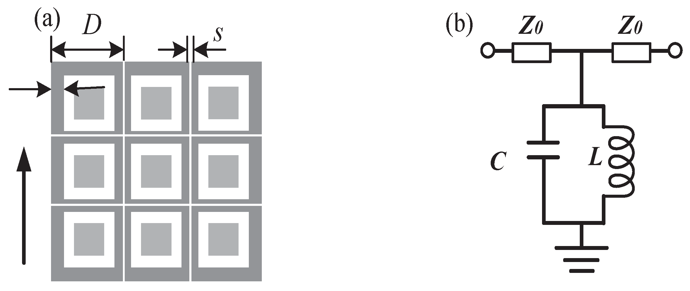
Figure 2.2.
Equivalent circuit model of second-order filtering structure.
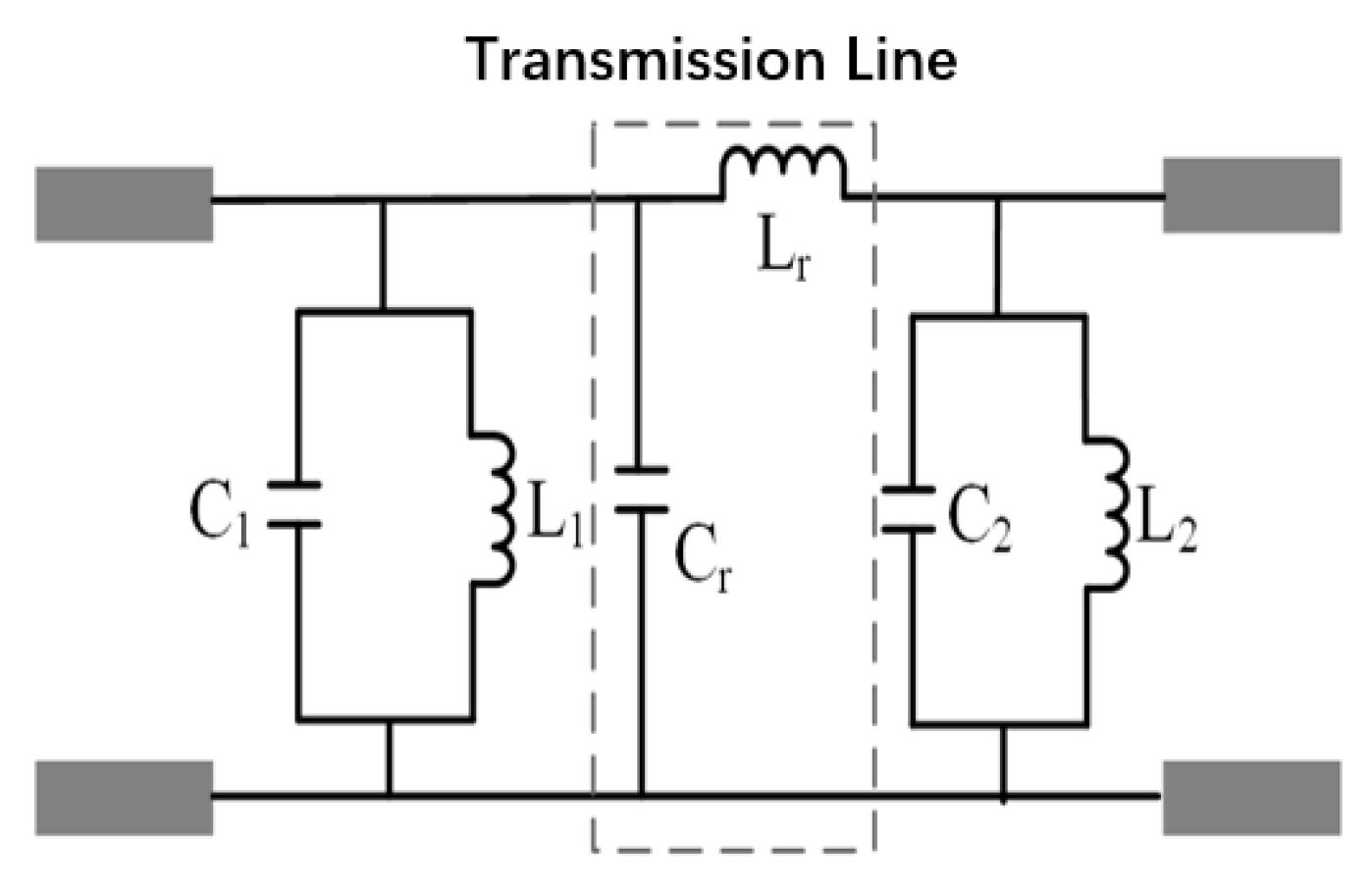
Figure 2.3.
Model of FSS ring structure with wideband characteristics (a)Structural Diagram(b)Overall Structural Cross-section.
Figure 2.3.
Model of FSS ring structure with wideband characteristics (a)Structural Diagram(b)Overall Structural Cross-section.
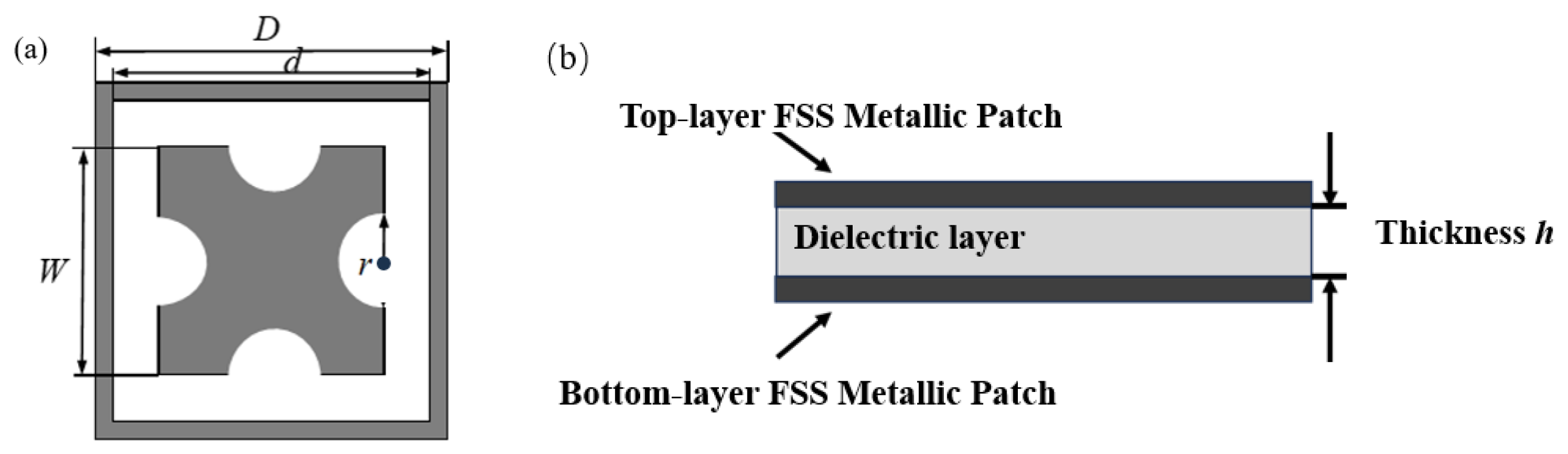
Figure 2.4.
Frequency Response characteristics of Broadband FSS.
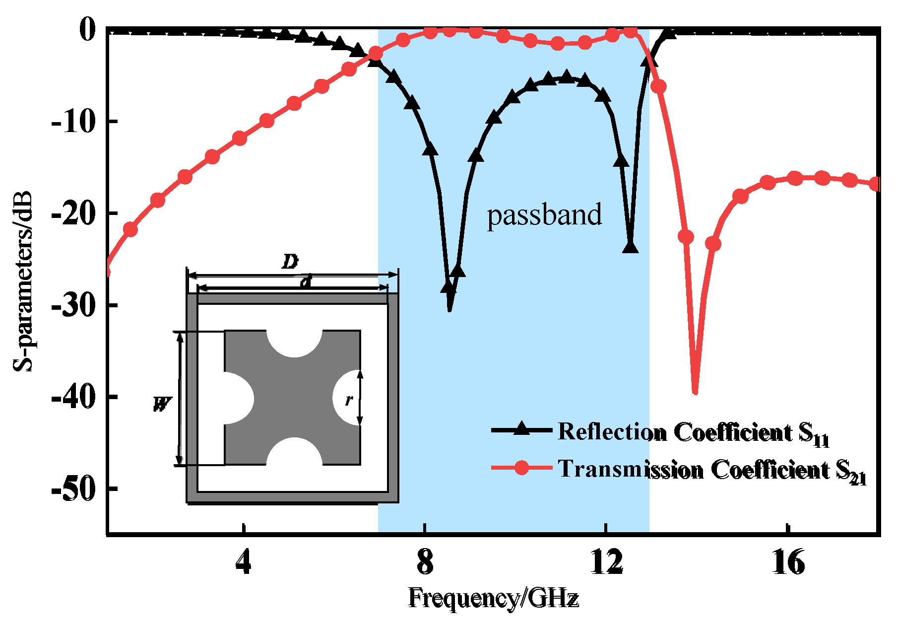
Figure 2.5.
Comparison chart of S11 curves simulated by CST/ADS.

Figure 2.6.
Frequency response characteristic curve at an incident Angle of 0-45° in TE polarization mode(a)Reflection coefficient S11(b)Transmission coefficient S21.
Figure 2.6.
Frequency response characteristic curve at an incident Angle of 0-45° in TE polarization mode(a)Reflection coefficient S11(b)Transmission coefficient S21.
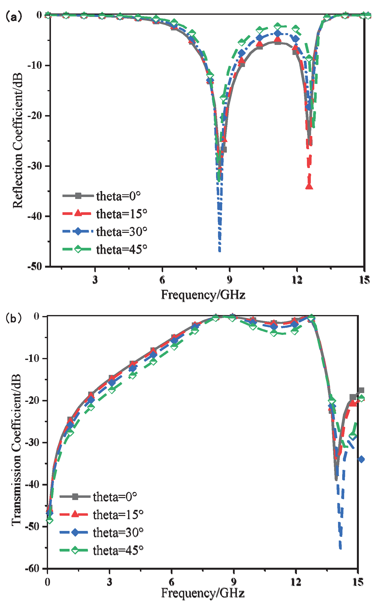
Figure 2.7.
Physical photo of broadband ring FSS.
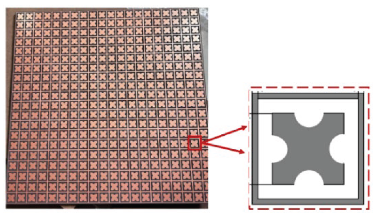
Figure 2.9.
Comparison of vertical incident test and simulation results of TE polarized electromagnetic waves.
Figure 2.9.
Comparison of vertical incident test and simulation results of TE polarized electromagnetic waves.
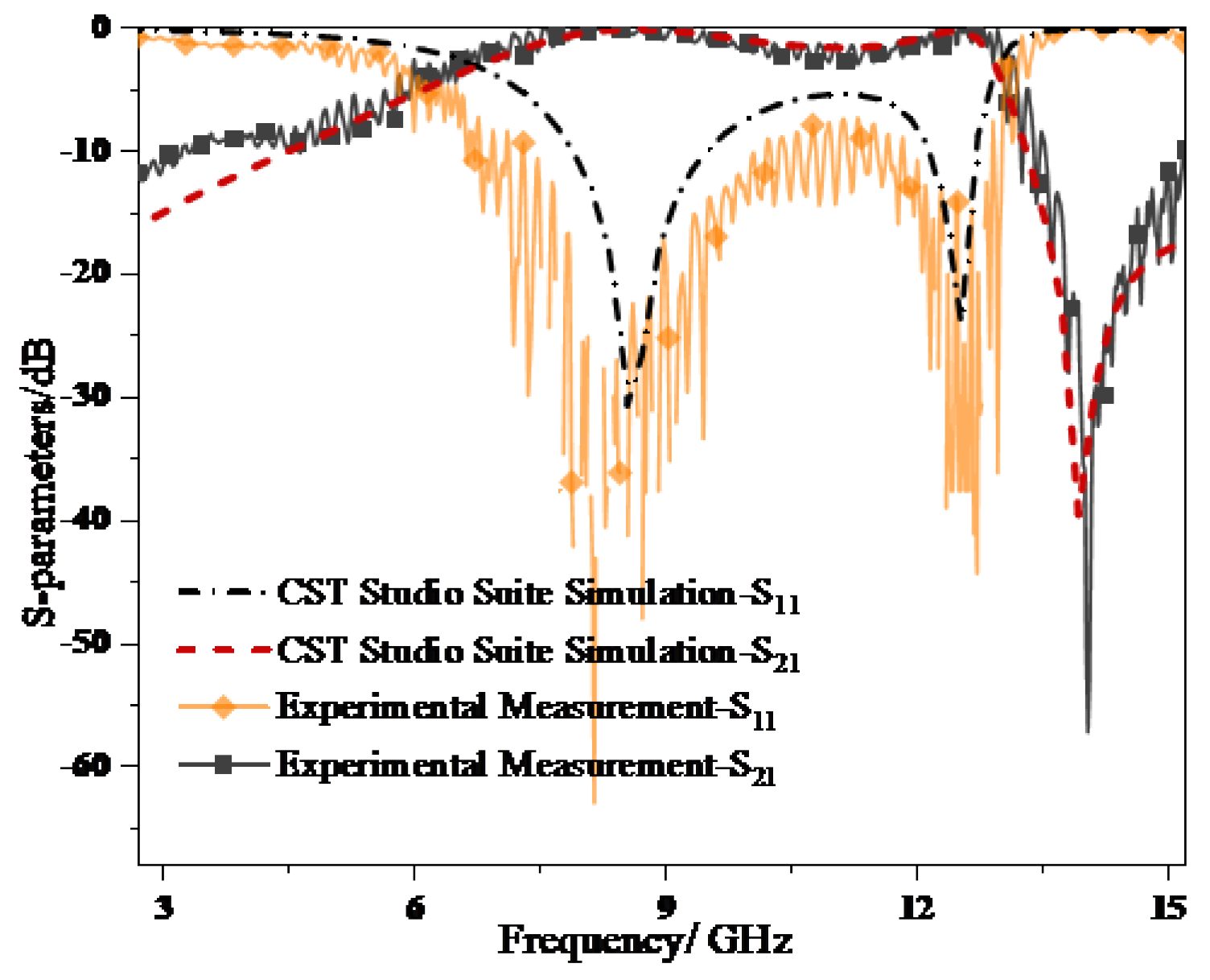
Figure 2.10.
Comparison of simulation results and test results when electromagnetic waves are incident at an Angle of 15°(a)Reflection coefficient(b)Transmission coefficient.
Figure 2.10.
Comparison of simulation results and test results when electromagnetic waves are incident at an Angle of 15°(a)Reflection coefficient(b)Transmission coefficient.
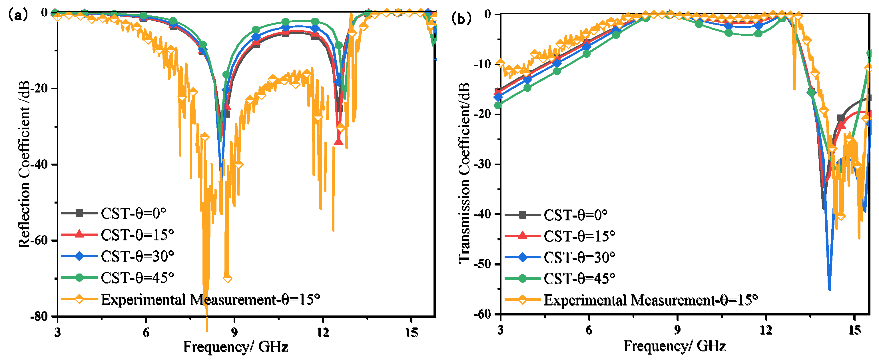
Figure 3.1.
Evolution process of the cross-bending structure and corresponding S parameters(d) Non-bent cross-shaped patch structure(e)Double-bent cross-shaped patch structure(f)Three-fold bent cross-shaped patch structure.
Figure 3.1.
Evolution process of the cross-bending structure and corresponding S parameters(d) Non-bent cross-shaped patch structure(e)Double-bent cross-shaped patch structure(f)Three-fold bent cross-shaped patch structure.
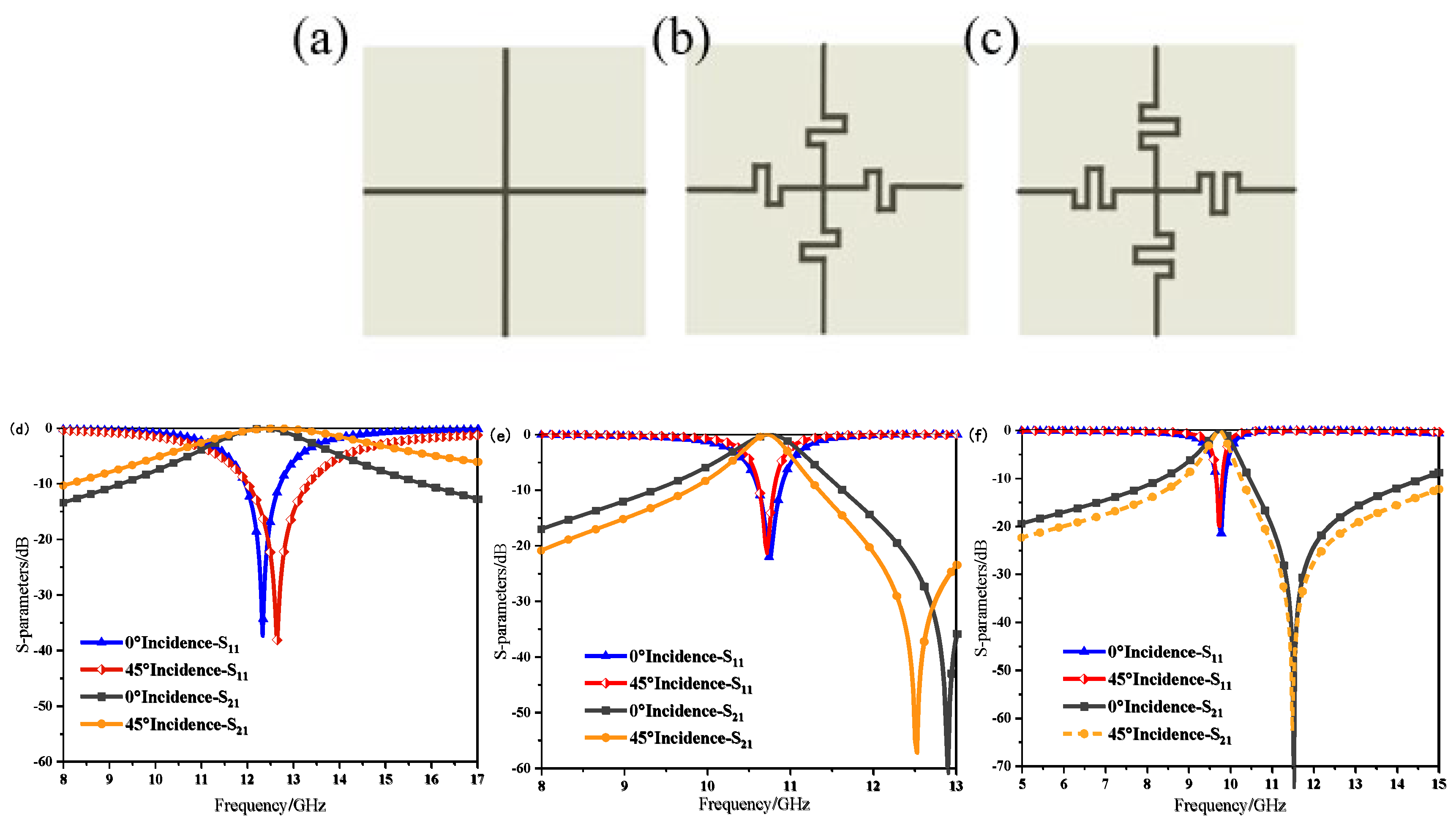
Figure 3.2.
Schematic Diagram of the reconfigurable AFSS structure(a)Overall structural schematic diagram(b)Schematic diagrams of the top-level and bottom-level structures(c)Schematic diagram of the structure of the middle feed layer(d)Structural section drawing.
Figure 3.2.
Schematic Diagram of the reconfigurable AFSS structure(a)Overall structural schematic diagram(b)Schematic diagrams of the top-level and bottom-level structures(c)Schematic diagram of the structure of the middle feed layer(d)Structural section drawing.
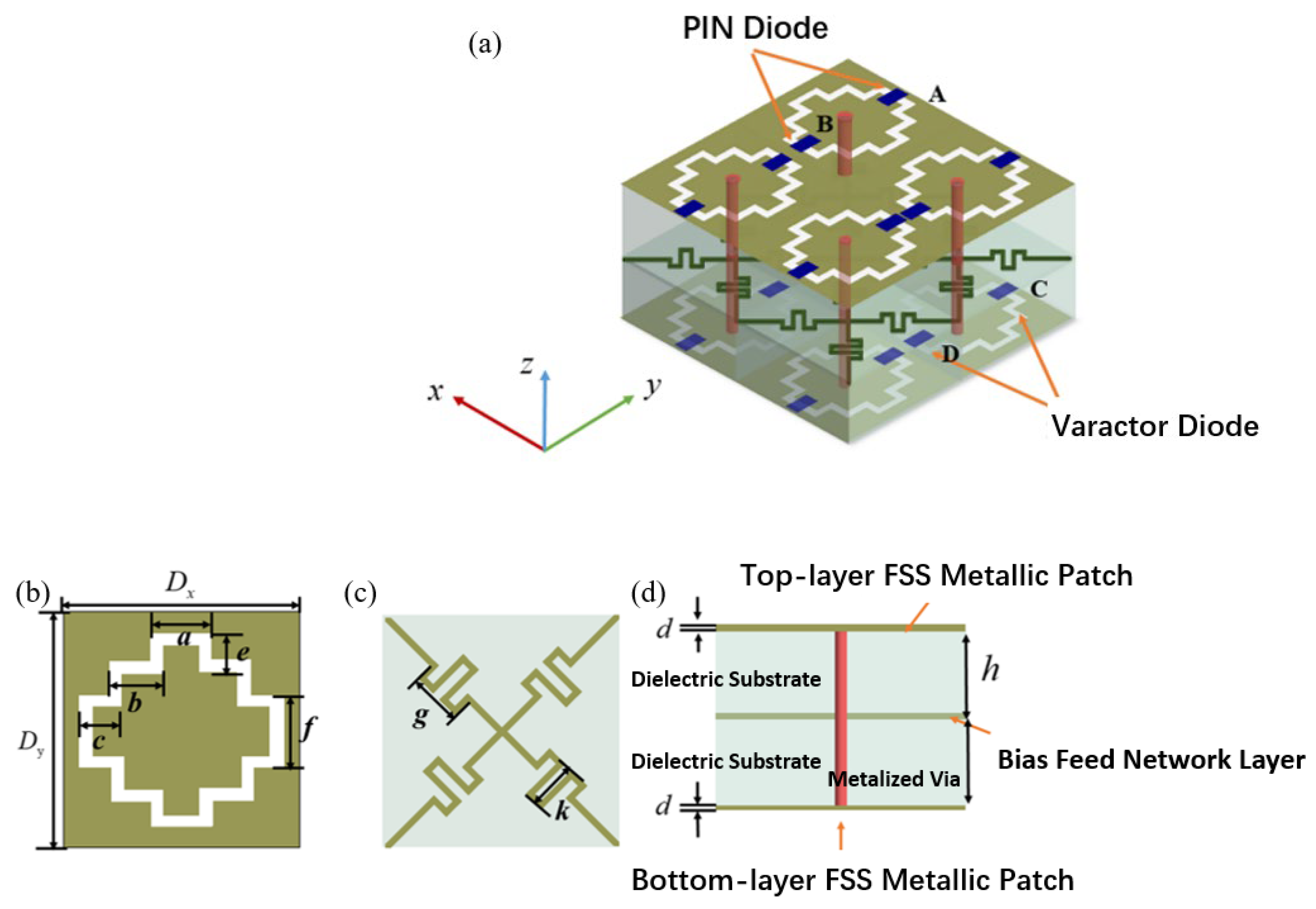
Figure 3.3.
AFSS frequency Response Curve.
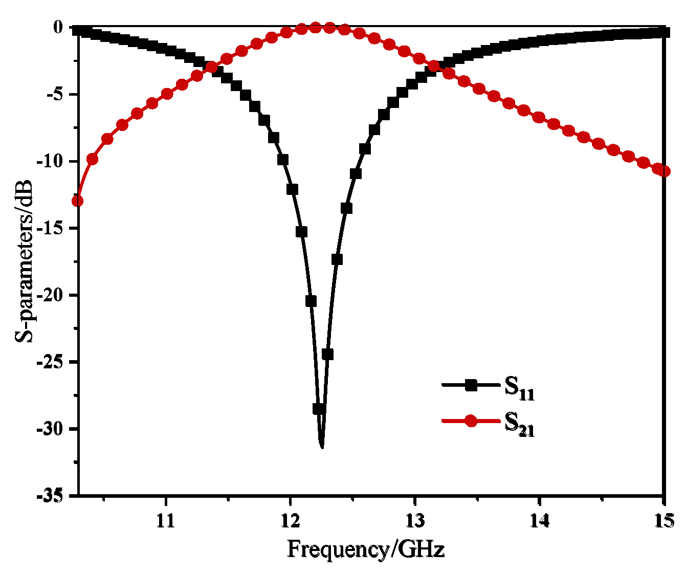
Figure 3.4.
Frequency response curve of AFSS structure when incident at an angle of 0-60°(a)Reflection coefficient(b)Transmission coefficient.
Figure 3.4.
Frequency response curve of AFSS structure when incident at an angle of 0-60°(a)Reflection coefficient(b)Transmission coefficient.
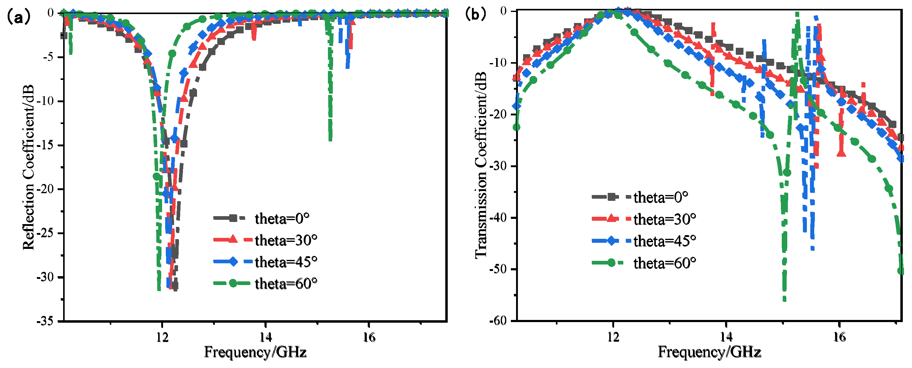
Figure 3.5.
Distribution map of electric field intensity at resonant frequency.
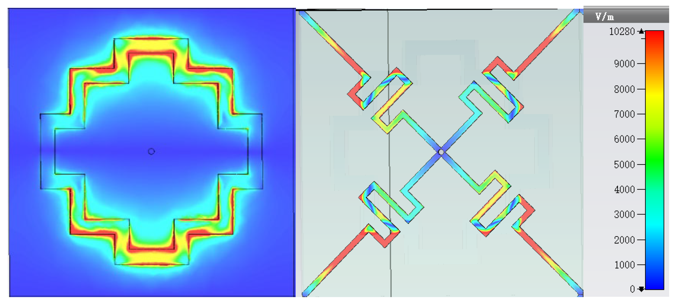
Figure 3.6.
Equivalent circuit model of the unit structure without loading diodes.
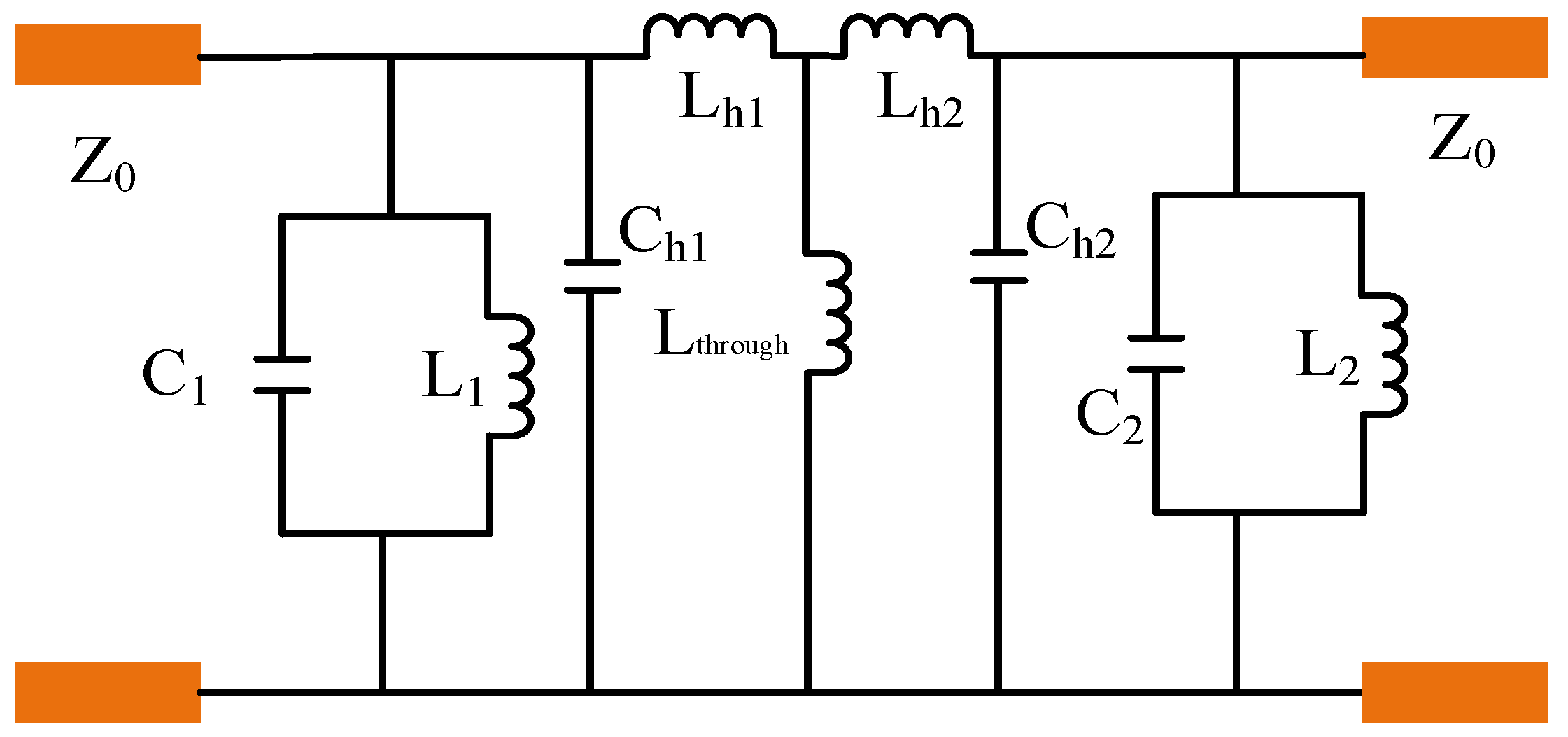
Figure 3.7.
Comparison chart of equivalent circuit model and reflection coefficient curve (S11)(a)Simplified equivalent circuit model(b)Comparison chart of ADS/CST simulation results.
Figure 3.7.
Comparison chart of equivalent circuit model and reflection coefficient curve (S11)(a)Simplified equivalent circuit model(b)Comparison chart of ADS/CST simulation results.
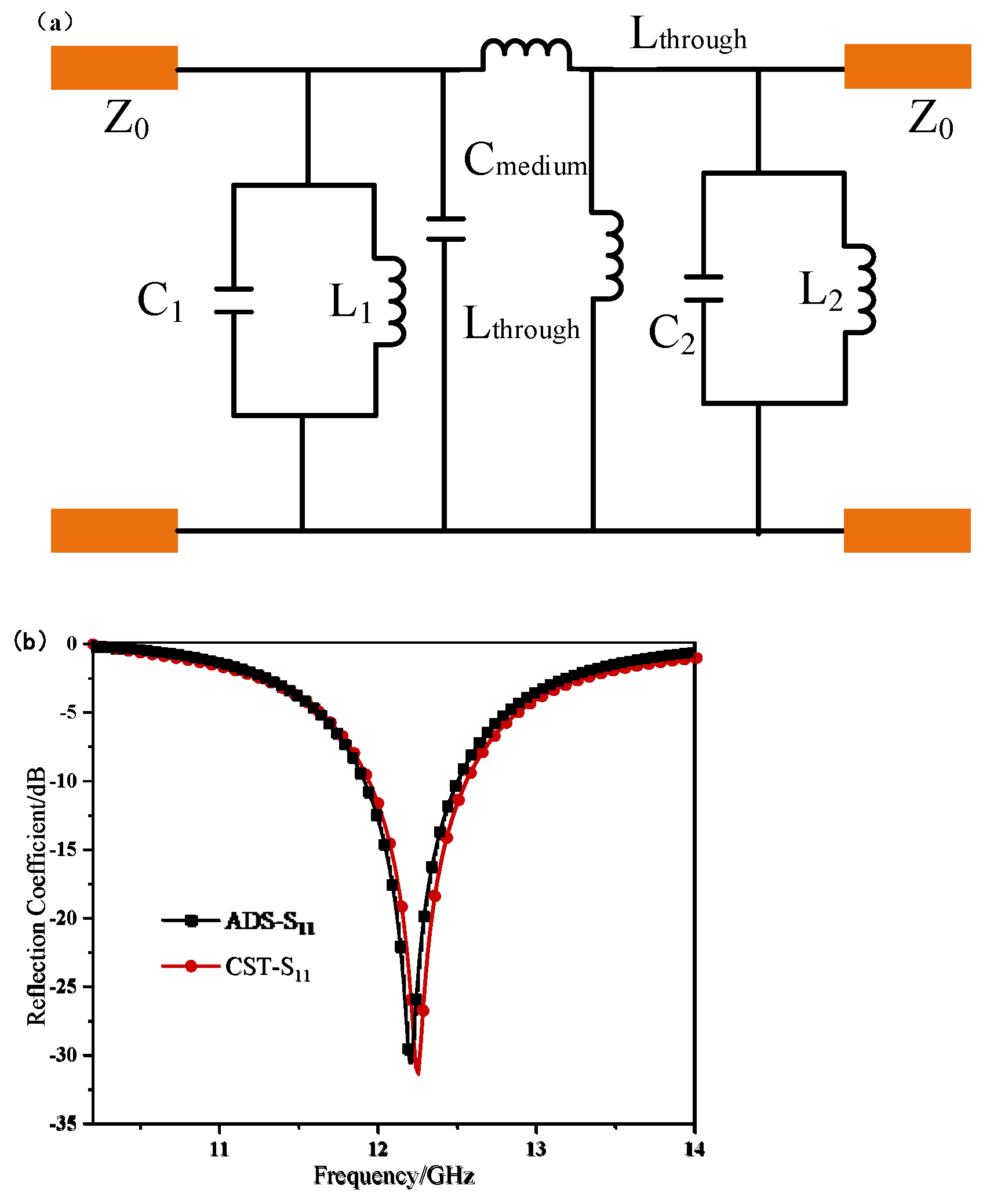
Figure 3.8.
Frequency response characteristics of diodes when they are on/off.
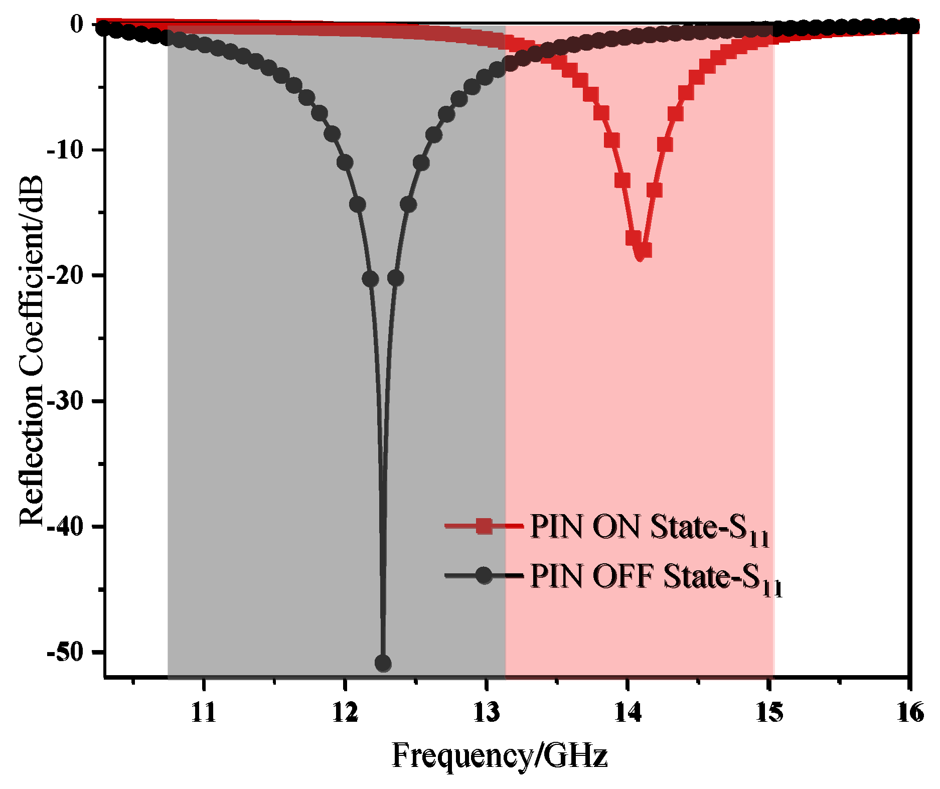
Figure 3.9.
Frequency response curves of the loaded PIN and varactor diodes.
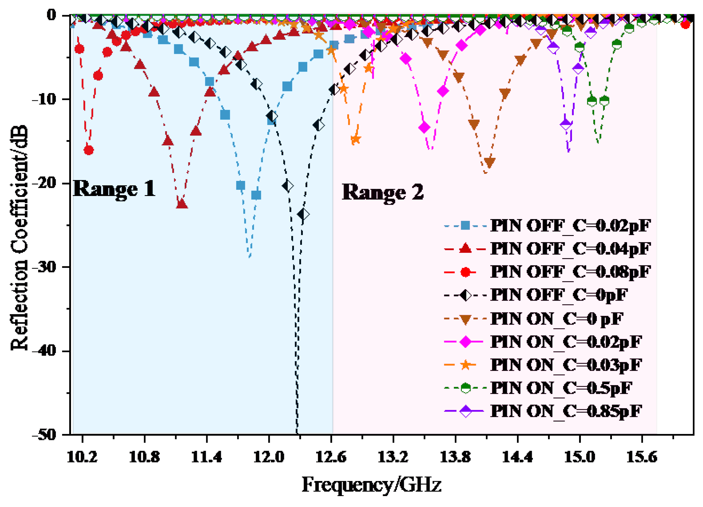
Figure 3.10.
shows the 0-60° oblique incident frequency response curve of the AFSS structure of the loaded diode(a)Reflection coefficient(b)Transmission coefficient.
Figure 3.10.
shows the 0-60° oblique incident frequency response curve of the AFSS structure of the loaded diode(a)Reflection coefficient(b)Transmission coefficient.
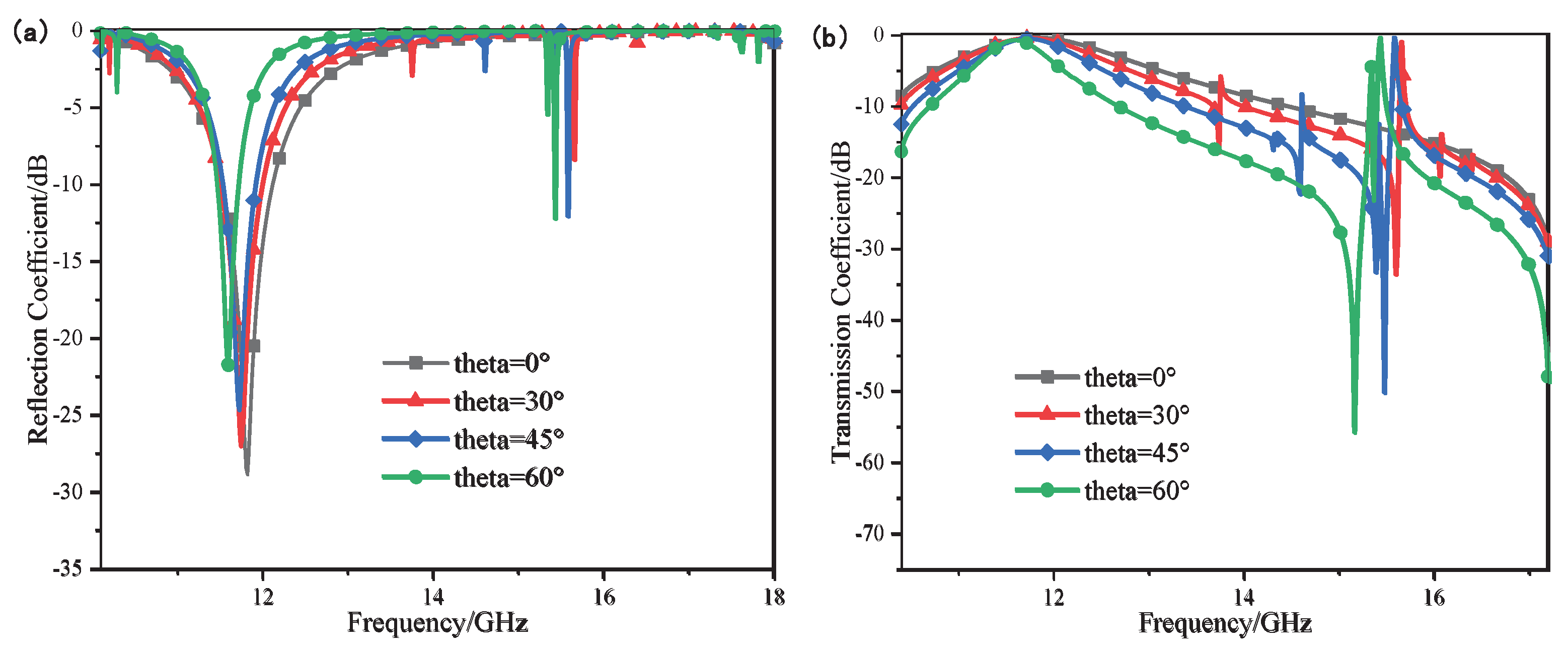

Table 2.1.
Unit Size Parameters.
| Parameter | D | d | W | Rtop | Rbottom | h |
| Value/mm | 10.0 | 9.0 | 6.7 | 1.0 | 1.1 | 1.575 |
Table 3.1.
Dimensions of AFSS Structural Model.
| Type | Dx | Dy | f | ||||||
| Value/mm | 10.00 | 10.00 | 2.60 | 1.56 | 1.04 | 1.04 | 2.60 | 2.00 | 1.78 |
Disclaimer/Publisher’s Note: The statements, opinions and data contained in all publications are solely those of the individual author(s) and contributor(s) and not of MDPI and/or the editor(s). MDPI and/or the editor(s) disclaim responsibility for any injury to people or property resulting from any ideas, methods, instructions or products referred to in the content. |
© 2025 by the authors. Licensee MDPI, Basel, Switzerland. This article is an open access article distributed under the terms and conditions of the Creative Commons Attribution (CC BY) license (http://creativecommons.org/licenses/by/4.0/).
Copyright: This open access article is published under a Creative Commons CC BY 4.0 license, which permit the free download, distribution, and reuse, provided that the author and preprint are cited in any reuse.


