Submitted:
31 July 2025
Posted:
07 August 2025
You are already at the latest version
Abstract
This perspective presents a novel physics approach in the field of electromagnetic and electronics engineering, combining the principle of metamaterials that may exist naturally in semiconductor electronic devices with parametric design and geometric optimization. By manipulating the geometric parameters of a simple transistor, diode, or resistor at the subwavelength scale, unexpected quantum localized oscillations can be achieved for their charge carriers (i.e., electrons), which can be triggered by inputting electromagnetic or electronic signals at specific frequencies that match their natural resonance frequencies. The proper and precise control of these tunable subwavelength physical phenomena will lead to an emerging electronics discipline focusing on creating engineered electronics and integrated circuits with unprecedented functionalities beyond the limits of traditional electronics and integrated circuits. The applications of parametric geometric meta-electronics span a wide range of active tunable detectors and emitters in any frequency band. This meta-electronic physical approach enables an alternative room-temperature solution to the fundamental extreme cooling requirements for superconductors and quantum computers.
Keywords:
parametric amplifications
; quantum superconductor
; meta-transistor
; quantum resonance localized oscillations
; metamaterials
; meta-devices
; superconductor qubits
; photonics neural network
; terahertz tunable detection and generation
; parametric geometric meta-electronics
; green energy harvester
History
Transistors were invented at Bell Labs in the mid-20th century. They have a maximum frequency limit called the unity gain frequency (ft), where the amplifier's gain becomes 1 (0dB). This limit is linked to the electron transit time τ in the device, expressed as ft = 1 / (2π τ). However, soon after transistors were invented, this frequency limit was surpassed [1,2,3]. Parametric Amplifiers (ParAmps) were first made using bipolar transistors. For example [2], a 50dB conversion gain and 7dB noise figure were achieved at 1000 Megacycles per second (1GHz) with a bipolar transistor that has unity gain frequency of 0.6GHz. Before transistor-based ParAmps, there were Silicon and Germanium p-n junction diode-based ParAmps [3]. The typical equivalent circuit of transistors for high-frequency use near and beyond their cut-off frequency are shown in (Figure 1a) and (Figure 1b). The dc instability in the transistor response was also reported (Figure 1d), and one way to use ParAmps was to use a transistor as a transit-time diode. The ParAmp circuit needs a tunable transmission line to match the desired frequency as a resonance cavity (Figure 1c), and the transistor can be tuned by its dc-current to reach resonance at only one specific current value. All this was done with circuits made of discrete electronic parts long before integrated circuits (Figure 1e). It was then accepted by scientists that transistors can amplify small signals beyond their cut-off frequencies without needing a new physical explanation. The next section briefly reviews the basic ideas of ParAmps.
During the 1950s and 1960s, the Cold War between the USA and the Soviet Union was intense. There was a demand for microwave communication systems with very low noise for various uses. Military electronics, especially radar, advanced a lot during this time. This might be why parametric amplifiers are not often mentioned in academic research, as the technology was highly confidential. Meanwhile, transistor technology improved with years, making transistors smaller and able to work at higher microwave frequencies normally with low-noise performance, and even reaching terahertz frequencies nowadays. However, Parametric amplifiers might still help pushing electronics to work at these higher frequencies in the terahertz and far-infrared bands.
In the 1960s and 1970s, scientists began studying how ultrasound waves and far-infrared light interact with the MOSFET channel's inversion layer. This layer was seen as a two-dimensional electron gas, and the movement of electrons or holes was called plasma oscillations [4,5,6,7,8]. These oscillations were studied at different temperatures, especially low ones. Researchers calculated different dispersion relations for these oscillations in various settings. They investigated how these oscillations could be detected and how stable or instable they were. A lot of this theoretical work was done by Russian physicist A.V. Chaplik.
Until the 1980s, the terahertz band (300GHz to 10THz) was called the THz gap because there were no sources for these frequencies. Chaplik's calculations showed that plasma oscillations could happen in this gap. Experiments were limited to two areas: the far-infrared range, beyond the transistor's cutoff frequency, and ultrasound waves, where the transistor was much smaller than the ultrasound wavelength.
In the 1990s, the advent of femtosecond lasers and other nonlinear electrical and optical terahertz (THz) sources catalyzed the experimental investigation of the THz electric response of transistors with various structures and materials, even surpassing their frequency cut-off limits. The theoretical framework developed by Shur and Dayknov [9,10,11,12] gained widespread acceptance, elucidating the THz response of transistors by incorporating the plasma oscillations model of Chaplik and emphasizing the linear dispersion relation of these plasma oscillations. The nonlinearity inherent in the transistor I-V characteristics has been exploited to rectify and mix electronic signals at frequencies significantly exceeding the transistor cut-off frequency. A key contribution of the Dayknov and Shur theoretical model is the application of the hydrodynamic equations of charge carriers (Euler and continuity) [12], which represent the standard transmission line (distributed RLC) model of the transistor channel (2DEG) and its surrounding dielectric material media.
At high frequencies, near and beyond the transistor cutoff frequency, the ultra-high-frequency Drude model must be considered, as it predicts the frequency-dependent conductivity and permittivity of the distributed RLC elements in the 2DEG model. By employing specific boundary conditions and assuming uniform carrier density in either gated or ungated 2DEG channels, the solution of the hydrodynamic equations corroborated the previously established possibility of plasma oscillations resonating in the 2DEG channel and the potential for current-tuned dc-instability due to an ac-induced negative conductance effect within the device's 2DEG channel. However, the Dayknov-Shur model, as well as the earlier Chaplik theoretical analysis, primarily focused on the so-called plasma oscillation in the 2DEG channel, neglecting other significant factors such as the THz coupling theory of electromagnetic waves with transistor deep-subwavelength structures and the potential frequency dependence of these electromagnetic coupling effects, which may modulate the transistor response with frequency in the absence of any plasma oscillation resonance or negative conductivity amplification within the transistor channels.
In another words, the transistor parts and the two-dimensional electron gas (2DEG) channel can handle very high frequencies because of the device's nonlinearity. But, the small size and shape of the device may cause a frequency-dependent effect, often mistaken for plasma oscillation peaks and valleys. In addition, Past theories (Chaplik, or Dayknov-Shur) do not help in making circuits that fix the device's DC instability and turn it into a stable setup for high-frequency tunable detectors and emitters. There is no tuning method into stabilization of these resonance effects, like those in parametric amplifiers, in previous studies of plasma oscillations. Also, the study of plasma oscillations does not fully cover the boundary between quantum physics and classical mechanics [13]. These plasma oscillations should be seen as quantum-localized oscillations, showing quantum effects as Chaplik predicted. However, they still fit within classical physics, described by classical equations like hydrodynamic models (transmission line theory) and simultaneously the Schrödinger equation with quantized modes. These localized oscillations appear as fields that decay quickly with distance in general, not as traveling waves. In some cases, the 2DEG's frequency-dependent impedance and nearby materials allow these oscillations to resonate at certain frequencies with specific quantized modes at a very small scale. These oscillations resonate at distances from a few nanometers to hundreds of nanometers, and possibly more.
Parametric Geometric Meta-Electronics
This new way of understanding how quantum waves behave in small transistors is linked to the well-known concepts about metamaterials. Metamaterials are being studied to create new features like tunability, switching, and sensing [14], [15]. The tiny structure of a transistor can be seen as a natural metamaterial structure. It has a pattern of parts that act as a deep subwavelength periodic transmission line element. This setup can change how the device works when it interacts with certain frequencies, allowing for negative conductance or impedance [16]. This means a regular transistor can become a "meta-transistor" with new abilities beyond normal electronics. The shape and materials of the transistor are important for matching the conditions needed for these quantum waves. The materials' electric and magnetic properties and the transistor's operating point affect how carriers move in the channels. We suggest calling this new field "Parametric Geometric Meta-Electronics" to explain these phenomena beyond just quantum waves in a 2DEG channel.
This Perspective Summary
This perspective explores the basic ideas behind parametric geometric meta-electronics. We talk philosophically about different theories related to previously called plasma oscillations. We highlight the quantum mechanical perspective of these quantum localized oscillations, correlating to the de Broglie-Bohm theory, which links classical and quantum physics. About 16 years ago, a significant development in parametric geometric meta-electronics took place. Elkhatib doctoral thesis [17] at the Terahertz Research Center at Rensselaer Polytechnic Institute studied for the first time the Terahertz (THz) response of field-effect transistors in the saturation regime. Elkhatib et al. observed active terahertz dc-rectifications [18] beyond the transistor cut-off frequency in transistors placed close together with subwavelength gaps. Another key experimental finding was the discovery of tunable room-temperature dc instability in field-effect transistors when specific THz ac signals were applied [19]. We offer a straightforward explanation of this active terahertz tuning mechanism. This mechanism has greatly advanced engineering technology over the past decade. Parametric geometric meta-electronics now have many applications across various frequency ranges, not restricted by traditional electronics or semiconductor limits. The main use of these tunable meta-devices could be in detecting and generating electromagnetic waves (EMW) with new unexpected performance levels. High-frequency communication systems with very high data rates are now possible, surpassing what current 3G-5G technology can achieve.
Another important new use is the deep subwavelength sub-THz and THz imaging technique [20]. Transistors can create images of terahertz radiation without needing an antenna or microstrip structures. But the obtained THz images need correlated adjustments to show the real electromagnetic waves hitting the device. This imaging method helps us see and study electromagnetic waves in tiny structures at many frequencies with very high details. The insights from this imaging are valuable because they let us see physical phenomena at small scales, instead of just guessing and testing later. Another use of these devices is making tunable sub-THz and THz lasers that work at many frequencies with very high precision. This new tuning method allows for precise lasing at any wavelength, unlike traditional lasers. The usual RGB color approximation method might become unnecessary with these tunable devices that can emit or detect many colors. However, visible light may be considered as electromagnetic waves with frequencies between 400-790 THz, and the device must be tuned to match these frequencies. New TVs could show true colors (Figure 2a), with each pixel emitting any adjustable frequency-locked light with almost pure colors. Similarly, new spectrometers and cameras could also detect electromagnetic waves at any adjustable frequency within very wide ranges as conceptually presented in (Figure 2b).
Harvesting Green energy is an important field in engineering due to the growing need for energy worldwide. Using adjustable transistors as special meta-devices can help detect electromagnetic waves over a wide range of frequencies. These devices can be used to make transparent solar panels (Figure 2c) that turn all solar spectrum (Figure 2d) into electricity with very high conversion efficiency more than any current technologies in the commercial markets. Other natural energy sources like sound and wind can also be harvested effectively with these devices with proper energy conversion. New types of batteries, called meta-electronics batteries, can last longer with less energy loss. Another exciting application of meta-electronics is with superconductor devices that work at normal temperatures. By adjusting certain oscillations, these devices can have almost no resistance at room temperature. This allows for new uses, like magnetic levitation, which can lead to fast and affordable transportation systems like Maglev trains. These adjustable devices have special features in both magnetic and electric fields.
Moreover, we point out two important uses for advanced artificial intelligence. Quantum computers are made to work at normal temperatures. They use quantum processors (Figure 2f), quantum memory, and photonic neural networks instead of regular digital processors, digital memories, and digital deep learning servers. A special quantum device with superconducting features can help design different qubit setups that work at room temperature. This solves the problem of needing very cold temperatures for traditional superconductors and helps with qubit design. Also, creating photonic neural networks (Figure 2e), inspired by the human brain, using adjustable arrays of small devices connected at a tiny integrated circuit level, can greatly improve AI technology. These improvements are expected to be much better than traditional digital electronics' neural networks in terms of energy efficiency, data processing speed, and simultaneously with smaller chips in size and cheaper in cost.
Throughout history, new technology has changed how we live. This has made people less interested in old knowledge and more focused on new ideas. For example, from the 1900s to the 1950s, TVs and radios used vacuum tubes. But when transistors were invented, they changed the electronics industry, making vacuum tubes outdated. Similarly, a new device called the tunable meta-transistor might change our knowledge significantly in the future. Today, meta-electronics learning is more important than old electronics ideas. The fifth industrial revolution started almost 15 years ago when Elkhatib experimentally verified the functionality of tunable meta-transistor. Soon, super intelligence using quantum computers and photonic neural networks might replace today's artificial intelligence. Super-fast communication and new devices will likely replace old methods, and new consumer meta-electronics products will take over from old ones. Also, better ways to collect energy and long-lasting batteries are expected to become available. The changes in the fifth industrial revolution are expected to be unlike anything before with much quicker technological shift and impact.
Parametric Amplifiers
In the early 1960s, Ulrich Rohde explained how to push transistor performance beyond their frequency limits [1], [2]. Figure 1 shows a simple high-frequency circuit of a basic bipolar transistor and how a parametric amplifier works. The transistor's current gain depends on frequency such as:
where αo is the common base current gain and fα is the cutoff frequency. Rohde suggested that the emitter and collector of the bipolar transistor act like a transmission line. This line connects to another output line with adjustable frequency (length). By adding adjustable feedback between the collector and base, negative resistance is created between the emitter and collector. This is explained by feedback amplifier theory [21], with the following equation:
Josephson parametric amplifiers (JPAs) [23], also known as superconducting parametric amplifiers, came from improvements in parametric amplifiers without the need of any transistors. JPAs are special because they have very low quantum-limit noise. They use the unique properties of Josephson junctions to make weak microwave signals stronger. One implementation of these JPAs is the flux-driven JPA [23] (Figure 3). It includes a coplanar resonator followed by a magnetic field-tuned device called a dc-SQUID, (direct current-superconducting quantum interference device). In the 1960s and 1970s, superconductivity only worked at very low temperatures. This made JPAs most useful for research and not for commercial use.
Plasma Oscillations in 2DEG
Understanding how electrons move in a thin layer as a two-dimensional electron fluid started with their use in microwave devices like klystrons and traveling wave tubes [24]. This electron fluid acts like a transmission line and follows fluid dynamics rules. Plasma oscillations, also known as Langmuir waves, can be created by adding another microwave source to the electron beam. These oscillations can have different patterns and modes in the electron beam. The electron beam is much longer than the wavelength of the microwave frequency used [25]. Sometimes, these oscillations can help amplify signals in a traveling wave tube, but other times, they can cause problems that might damage the tube. These problems are due to negative differential resistance seen in the current voltage (I-V) characteristics at the collecting-emitting electrodes. The speed of electrons in the direct current electron beam can change the frequency of these plasma oscillations, like the Doppler effect.
After the invention of field-effect transistors and high-electron-mobility transistors, scientists worked hard to understand how electrons move in these devices. They compared this movement to a fluid-like electron beam in a microwave tube. However, they mostly ignored how electromagnetic waves interact with small structures (subwavelength sizes). Instead, they focused only on modeling how electron gases behave, without considering the shape and size of the materials around them. For example [5], a MOSFET transistor with a special gold diffractive gate (Figure 4a) was used to change signals in the far-infrared range. But instead of studying how EMW at terahertz frequencies interact with this device as a meta-device, researchers used plasma resonance to model the signal changes. This led to wrong conclusions about how terahertz frequencies work with the device (Figure 4b). If real plasma resonance happened in these small structures, there would be clear resonance effects with multiple frequency peaks. Many theoretical models of these plasma oscillations are seen as abstract ideas that don't accurately show how different small structures respond. Technology Computer-Aided Design (TCAD) simulators are essential to study this problem. TCAD numerical solvers use precise calculations to study how these structures behave, considering complex electromagnetic fields, device physics, metamaterials structure, and even quantum effects. These tools are crucial for exploring new areas in meta-electronics and they are still in the early stages of development.
Quantum Localized Oscillations
Graduate students who study solid-state physics should understand phonons, crystal vibrations, and how to estimate dispersion relations and calculate group velocity. They also learn about more advanced topics like longitudinal and transverse modes for optical and acoustic dispersion relations. Based on these basics, we find common misunderstandings in modeling plasma oscillations in the two-dimensional electron gas (2DEG) of any channel. For plasma oscillations to resonate, the dispersion relation must have a zero slope, showing a standing wave, not a traveling wave. But current models often focus on the long-wavelength limit, where frequency is directly proportional to the wavevector:
which inaccurately describes plasma oscillations in very small dimensions under resonance. On the other hand, the 2DEG in a field-effect transistor channel can be seen as a one-dimensional free electron Fermi gas [26], especially in a very wide transistor channel with a very short length L. In quantum physics, the electron fluid is limited to a length L, and the wavefunction of the electron fluid oscillations is found by solving the Schrödinger equation with boundary conditions at both ends of the channel. Without going into complex quantum math, only certain oscillation modes are possible solutions for the wavefunction, with different chances of being in these modes. There are also band gaps where these quantum-localized oscillations do not occur. The temperature of the 2DEG greatly affects the likelihood of these oscillation modes, as shown by the Fermi-Dirac distribution.
Field-effect transistors have a channel where electrons move like a fluid. We can study this using simple physics equations from transmission line theory (Figure 5a). The movement of electrons is explained by Euler and continuity equations [12]. This topic connects classical physics and quantum mechanics [13], helping to bridge the two. In transmission line theory, electron movements usually decay quickly in a transistor’s channel, with a specific characteristic length showing exponential decaying behavior [27]. This happens in a frequency range where Schrödinger equation doesn't have solution. When the input frequency matches the natural frequency of the 2DEG channel and its surrounding material, a special kind of oscillation occurs (see Figure 5f). This is like sound waves standing still in a tube. The chance of these oscillations depends on the structure's shape, size, temperature, and any extra electric or magnetic fields. When the electron fluid hits this special condition, the flow of electrons or holes in the 2DEG becomes unstable (Figure 5d). This can lead to uncontrolled amplifications unless the energy is absorbed and balanced.
Let's look at an example to explain solid-state physics in simple terms. During an earthquake, strong vibrations spread quickly from its epic center over large field distances. Buildings in this area are very small compared to these waves. If the earthquake causes the building to shake at its natural frequency, it can become unstable and might collapse quickly. But if we add extra parts to the building, it can handle the shaking without falling. This is similar to how electromagnetic waves or electrical signals interact with a two-dimensional electron gas (2DEG) surrounded by a special dielectric material. When the signal's frequency matches the natural resonance frequency of the structure, it causes strong resonance oscillations, making the device unstable due to uncontrolled self-amplifications. This can lead to device breakdown unless we use some circuit configuration to absorb and balance this energy.
The Missing Tunability Mechanism in Metamaterial
When designing or using a parametric geometric meta-device, it's important to find the natural resonance frequency of the tiny microscale or nanoscale structure. Adjusting this resonance is the tuning key for each device. Theoretical models often can't capture all the details needed to find these resonance modes, especially in complex structures. Simple models might work for basic structures like one-dimensional electron gases or simple metal wires, but electromagnetic coupling can change the expected resonance in these small structures. Numerical solvers for these devices are still being developed, and they need to include semiconductor device physics, electromagnetic basics, and metamaterial principles, along with quantum effects. Experimentally, researchers need to test a wide range of frequencies to find the natural resonance modes, which are in the terahertz range. This makes precise testing hard. Strong terahertz sources with precise frequency control are needed to find the resonance mode of a specific structure. Although the potential of the terahertz range was first explored in the 1980s, it wasn't until 2010 that reliable, tunable sources were available to test the entire terahertz band for each device's natural resonance.
Advancements in research and technology in metamaterials for photonics have helped control quantum-localized oscillations using different optical structures. Quantum dots in one, two, and three dimensions, along with periodic structures with a negative refractive index, are subwavelength meta-optical devices [28,29,30]. These devices use quantum-localized oscillations to achieve natural resonance conditions that go beyond classical optics and materials. However, a major challenge for all meta-devices is their tunability. Once a meta-structure is designed and made with subwavelength dimensions, it has specific natural frequency resonance conditions that cannot change. The frequency must always match the natural resonance mode of the structure. This geometric limitation restricts the range of designs and frequency applications that can be developed. Some studies suggest combining MEMS and NEMS technology with metamaterial structures to create tunable optical meta-devices by changing their geometry. But mechanical tuning is less reliable than electronic tuning and offers fewer design possibilities and applications.
Simple Field-Effect Transistor as a Meta-Resistor
The world might be on the moment of re-discovering the transistor capabilities and might re-think how we use transistors. Transistors have changed electronics a lot in the last 75 years, and their impact on our lives is well known. In parametric geometric meta-electronics, the link between transistor size and speed doesn't matter anymore. So, making transistors smaller isn't as important now. We don't need tiny transistors to make fast circuits. Old semiconductor fabrication methods can make advanced devices at any frequency, no matter the transistor's size or material. In some cases, a larger transistor can work just as well as a smaller one. However, smaller transistors are still important for fitting more circuits on a chip. For example, a 1µm transistor can detect or emit visible light and millimeter waves simultaneously. Visible light has wavelengths from 400 to 790 nm, which is smaller than 1µm, while millimeter wavelengths are (1 to 10 mm) much larger than 1µm.
In basic terms, a field-effect transistor works like a simple resistor [31]. Its resistance is set by the slope of its current-voltage graph when the transistor is near zero-drain voltage or has very low direct current (DC). The abstracted theoretical model by Dayknov and Shur says that plasma resonance in gated channels depends on the resistor's length and the gate voltage, which changes the carrier density in the channel. So, the transistor can be tuned with a small DC current and gate values to get resonance across the channel. However, there is a basic problem with the Dayknov-Shur model. It uses the DC gradual channel approximation to link the carrier density in the transistor channel to the gate voltage as:
Where ns is the free carrier’s density in the channel, e is the electron charge, Vgs is the voltage between the gate and source, and Vth is the transistor threshold voltage. Using the direct current gradual channel approximation is like modeling the transistor channel at high frequency, focusing only on dc resistivity (the real part of complex conductivity) [27]. However, solving the hydrodynamic equations for the transistor channel requires considering complex conductivity that changes with frequency, as explained by the Drude model as:
Where is the angular frequency and τ is the electron transit time. Finding an exact analytical solution to the hydrodynamic equations at high frequencies might be little hard. If we only look at the DC RC transmission line model of the transistor channel, the solution becomes near-field evanescent waves that exponentially decay from the edges of the channel, leading to only DC rectification at the transistor ends. Also, for resonance oscillations in the whole transistor channel, there must be a standing wave with no traveling wave solution, and the dispersion relation must have a flat zero slope. It is not practical to use a linear dispersion relation for a traveling wave model in a very deep subwavelength meta-structure.
We strongly believe that at room temperature, it is very hard to see strong quantum-localized resonance oscillations in a resistive channel with almost no drain bias. The interaction of electrons with other electrons and phonons increases channel resistance, weakening the applied THz oscillations. By cooling the transistor to very low temperatures, the resonance modes might be clearer throughout the channel, and DC instability happens along the whole channel at early THz frequencies. This extreme cooling, below the superconductivity critical temperature (Tc), turns the transistor channel into a tiny superconductor channel with almost no resistance for the total channel length, where electrons have few or no collisions with other electrons and phonons. Electron movement in the channel can be seen as ballistic transport in a superconductor wire, as explained by the Shur-Eastman analysis [32].
Simple Field-Effect Transistor as Tunable Meta-Device
Identifying a natural resonance condition within any fixed-length or geometric meta-structure presents a significant challenge, akin to a complex game of hide-and-seek. This difficulty arises due to the absence of precise numerical models and the limited availability of experimental terahertz (THz) sources as mentioned before. Even transistors, which can be slightly adjusted near the zero-drain bias by altering the small direct current or gate voltage, fail to detect this resonance at room temperature. We found a theoretical and experimental gap exists concerning the application of field-effect transistors for tunable terahertz detection and generation. This gap pertains to the behavior of transistors operating in the saturation regime when the channel length is not fixed (Figure 5b). No analytical model currently exists due to the nonuniform carrier distribution in the transistor resistive channel, with certain regions being completely depleted (Figure 5c). Elkhatib [17], in his doctoral research at Rensselaer Polytechnic Institute, conducted the first detailed experimental investigation into the THz response of field-effect transistors in the saturation regime.
The direct current rectifications were enhanced due to active rectifications [18] beyond the transistor cutoff frequency. Furthermore, the coupling of THz radiation undergoes significant changes, facilitating accurate correlated subwavelength imaging of fallen THz radiation [20], in contrast to the disrupted THz coupling observed when transistors function as simple resistors near zero-drain bias conditions. Concurrently, Elkhatib made a significant discovery in experimental physics, revealing that a transistor channel can exhibit unique natural resonance conditions and DC instability [19] at 1.6THz and 0.2THz when operating deeply in the saturation regime (Figure 5d). This phenomenon occurs at room temperature, even surpassing the typical frequency limits of transistors. This constitutes the first experimental evidence of room-temperature superconducting behavior above the critical temperature, attributed to special quantum-localized resonance oscillations in the depleted region of the transistor channel.
Here, we summarize the theoretical interpretation of this breakthrough experimental discovery. In a certain state of the transistor, electrons (or charge carriers in general) move from one end of the resistive channel edge to the other end of the drain at a steady speed called saturation velocity [31] in the depleted region with length Lo (Figure 5b). This distance is varying in small ranges, from only a few nanometers up to 100s of nanometers. The thin layer in the depleted region acts as a small adjustable one-dimension quantum wire for the current at room temperature, whereas the transistor channel width is much wider, in the order of tens or hundreds of micrometers.
In general, THz input radiation is coupled simultaneously from the source and drain terminals into the transistor channel. Typically, evanescent subwavelength oscillations decay exponentially very quickly at both the source and drain sides of the transistor resistive channel (Figure 5e). At the drain side, the rectified AC oscillations at the source side are actively rectified with gain, whereas the AC oscillations at the drain side do not play any significant role in the rectified signal at the drain side. Until the length of the depletion region Lo and the saturated electron current density within this depleted region match the natural quantum resonance condition of the applied THz signal at the drain side. Different quantum resonance conditions (Figure 5f) can be set for the same input frequency by adjusting the drain current, gate voltage, and load resistor. The total length of the transistor channel does not affect the quantum-localized resonance condition. The key part is the length of the depleted region Lo, and the input THz frequency should be applied at the drain side, not at the source side, as suggested by the Daykinov-Shur model. The Input THz frequency at source side are still Evanescent oscillations that are decaying exponentially in the short resistive part of transistor channel
Under this quantum wave resonance condition, the depleted region also behaves like a tiny quantum superconductor wire at room temperature. Here, electrons move without resistance, surrounded by semiconductor ions and without colliding with other particles or phonons. We suggest calling this phenomenon: the Elkhatib-Elnahwy TQSWE (tunable quantum superconducting wire effect). The natural quantum resonance oscillations can be adjusted at any frequency, regardless of the semiconductor material. These resonance oscillations cause instability in the transistor current. This effect can be described as a DC-current instability induced by AC quantum resonance condition. These quantum oscillations can be considered as tiny transmission lines with only LC elements, separated from the rest of the resistive channel. They can also be studied using quantum physics by solving the Schrödinger equation to determine the wavefunctions that fit the depleted region (Figure 6). If the resonance condition is not met, there is no wavefunction solution, and the oscillations at the drain-side edge decay slowly in the depletion region and then decay quickly and exponentially in the resistive channel, with only stable DC rectification observed.
Stabilization of Dc-Instability in Meta-Transistor
The Elkhatib-Elnahwy TQSWE pertains to a specialized type of superconducting wire utilized in field-effect transistors (FETs), which operate effectively at room temperature as well as at both elevated and reduced temperatures. This represents a substantial advancement in scientific understanding and has already begun to influence technology and knowledge over the past 15 years, with expectations of continued impact in the coming few decades. However, translating this discovery into practical technology presents a considerable engineering challenge. It is crucial to ascertain how this discovery can lead to the development of new commercial products. The fundamental principles of traditional parametric amplifiers can facilitate the creation of devices that operate beyond conventional electronics limits. Amplifier feedback theory is also pertinent in this context.
The well-established differential voltage-controlled ring oscillators [33] (Figure 7A) may offer a straightforward method to harness these uncontrolled self-amplifications, which arise due to quantum effects in the transistor depleted region. It is essential to connect a load resistor to the transistor to observe these effects. The ring oscillators manage the excess energy and maintain certain energy equilibrium condition. A single-pair differential ring oscillator has limitations; thus, a three-stage (or more) ring oscillator may provide more effective results. Given that the depleted region behaves like a superconductor with near-zero resistance, designing an LC oscillator is an even more promising approach. A cross-coupled oscillator [33] with an additional current source is a superior option as it permits tuning without altering the power supply (Figure 7B). The Colpitts oscillator [33] is another viable alternative, employing one transistor, feedback capacitances, and a current source to adjust the resonance oscillations (Figure 7C). It is noteworthy that numerous meta-electronics concepts may be applicable here, where multi-stage amplifications and cascade designs can be implemented. Tunable emission and detection are feasible at any locked frequency, independent of the semiconductor material or bandgap limit.
Conclusion
For many years, scientists and academics all over the world have been trying to achieve room-temperature superconductivity. This effect was simply found in the depleted region of field-effect transistors operating in the saturation regime at quantum localized resonance condition. To make this big step forward, the world needed to understand the tiny details of subwavelength physics and how things work at a very small microscale or nanoscale level. Once we understand these details, we can use them in more ways. We don't need to make tiny transistors to make big technological progress. Small spaces within the transistor depletion region can change technology again, like when transistors were first invented 75 years ago. This is seen as a second rebirth for transistor technology that is leading the 5th wave of industrial revolution through an emerging leap of parametric geometric meta-electronics. Instead of regular electronic computers, we can now think about having quantum computers at home and exploring new levels of super intelligence beyond the current artificial Intelligence drawbacks. Also, harvesting energy becomes much easier. But we must remember that any technology can have bad sides. Energy weapons, in particular, are very dangerous and can cause a lot of harm without killing. So, we invite the world to be careful and not allow dangerous uses of this technology by irresponsible terrorist organizations. From Cairo University in Egypt, we suggest using this technology wisely, learning from the past. It is better to use parametric geometric meta-electronics to improve life rather than cause harm and destruction.
Notes:
1: This humble academic work is nominated for the Noble Prize in Physics
2: the text and all images in this article are humanized AI enhanced ones with fully paid service.
3: This article was initially written in July 2010, and it has been on hold due to its national security value and highest confidentiality, it has been minorly re-edited and improved in quality to be submitted for publicity in 2025.
Acknowledgments by Tamer Elkhatib
This work is dedicated to the memory and spirit of my esteemed teacher and mentor, Professor Salah Eldin Ameen Elnahwy, who passed away few years ago before the possible submission of this article. I extend my gratitude to Rensselaer Polytechnic Institute (RPI) for awarding me a graduate scholarship throughout my PhD studies in the United States, as well as for the opportunity to engage in research on Terahertz Electronics Technology within their laboratories. I am also grateful to my colleagues at the Center of Terahertz Research at RPI for their invaluable support and guidance in operating complex laboratory equipment, as well as their assistance in co-authoring publications derived from my own experimental findings. I express my appreciation to the Faculty of Engineering at Cairo University for providing a valuable, tuition-free master's education in engineering physics discipline with double major in both physics and engineering, which causes my well-developed experimental physics skills as well as my good understanding of wide range of theoretical physics fundamentals beside electronics. Special acknowledgment is due to Professor Sherief Abd El-Azem, who imparted to me the significance of ethics within the engineering discipline in his undergraduate course. I believe that my adherence to ethical principles, alongside the scientific and academic breakthroughs presented in this work, may have contributed mostly to my nomination for such a prestigious award in physics. Last but most importantly, I express my gratitude to Allah, the creator of the universe, for his inspiration, support, and blessings, and I pray for his continued favor upon me.
Author Contributions
Salah ELnahwy made the guidance to experimentally study THz response in the saturation regime and lead the theoretical interpretation of the experimental results of active rectification and quantum superconducting wire effect at room temperature. Tamer Elkhatib, design and run experimental studies of THz response in the saturation regime. Elkhatib also suggested and tested all circuit solutions for stabilizing the dc instability observed in transistor channel due to the self-amplifications of quantum wave resonance. Both Salah Elnahwy and Tamer Elkhatib share the contribution for the wide possibilities of different applications coming out of this scientific breakthrough discovery.
References
- Rohde, U.L., Pushing Transistors Above Their Frequency Limits with Parametric Conversion operation. Electronics 35, 25, 46-49 (1962).
- Rohde, U.L., Parametric Amplification, Wireless World, October (1961).
- Tien, P.K., Heffner, H., Parametric Amplifiers, journal of research of the national bureau of standards, section D, Radio propagation, 64D, 6, 751-752, (1960).
- Chaplik, A.V., Possible Crystallization of Charge Carriers in Low-density Inversion Layers, Sov. Phys.—JETP, 35, 2, 395-398 (1972).
- Allen, S. J., Tsui, D. C., Logan, R. A., Observation of the Two-Dimensional Plasmon in Silicon Inversion Layers. Phys. Rev. Lett. 38, 17, 980-983 (1977).
- Krasheninnikov, M.A., Chaplik, A.V., Resonance excitation of hypersound by two-dimensional plasmons, Sov. Phys.—JETP 49, 921-923 (1979).
- Magarill, L.I., Chaplik, A.V., Quantum effects in the absorption of a Rayleigh wave by two-dimensional electrons, Sov. Phys. JETP, 66, 6, 1289- 1292 (1987).
- Nakayama M., Theory of Surface Waves Coupled to Surface Carriers, Journal of the Physical Society of Japan, 36, 2, 393-398, (1974).
- Dyakonov, M., Shur, M., Shallow water analogy for a ballistic field effect transistor: New mechanism of plasma wave generation by dc current, Phys. Rev. Lett., 71, 15, 2465-2468, (1993).
- Dyakonov, M., and Shur, M., Detection, mixing, and frequency multiplication of terahertz radiation by two-dimensional electronic fluid, IEEE Trans. Electron Devices, 43, 3, 380-387 (1996).
- Dyakonov, M., Shur, M., Current Instability and plasma wave generation in ungated two-dimensional electron layers. International Journal of High-Speed Electronics and Systems, 16, 02, 443-451 (2005).
- Dyakonov, M., Shur, Plasma wave electronics: Novel terahertz devices using two-dimensional electron fluid, IEEE Trans. Electron Devices, 43, 10, 1640–1645, (1996).
- Allori, V., Zanghì, N., On the Classical Limit of Quantum Mechanics. Found Phys 39,1, 20–32 (2009).
- Lapine, M. et al., Structural tunability in metamaterials, Appl. Phys. Lett., 95, 8, 084105 (2009).
- Tao, H. et al. Reconfigurable terahertz metamaterials, phys. Rev. Lett. 103, 14, 147401(2009).
- V. G. Veselago, The electrodynamics of substances with simultaneously negative values of ε and μ. Sov. Phys. USPEKHI 10, 509–514 (1968).
- Elkhatib, T. A., Terahertz detection and imaging using field effect transistors operating in the saturation regime, Doctoral Thesis, Troy, New York, RPI, (2010).
- Elkhatib, T. A., et al., “Terahertz response of field-effect transistors in saturation regime,” Appl. Phys. Lett., 98, 24, (2011),.
- Elkhatib T.A., “Tunable Sub-THz and THz Lasing Effect using FETs at Room Temperature” preprint, DOI:10.48550/arXiv:2411.02605, Nov. 2024. (Submitted to Phys. Rev. Lett.).
- Elkhatib, T. A., et al., Subwavelength detection of terahertz radiation using GaAs HEMTs, Proc. 8th IEEE sensors Conf., 1988-1990 (2009).
- Razavi, B., Design of analog CMOS integrated circuits, New York, 246-290, (McGraw Hill 2001).
- J. M. Manley and H. E. Rowe, Proc. IRE 47, 2115-2116 (1959).
- Yamamoto, T., Flux-driven Josephson parametric amplifier, Appl. Phys. Lett. 93, 042510 (2008).
- Kompfner, R., "The Traveling-Wave Tube as Amplifier at Microwaves," in Proceedings of the IRE, 35, 2, 124-127 (1947).
- Chu, L. J., Jackson, J. D., Field theory of traveling-wave tubes, Proceeding of the I.R.E.,36,7,853-863, (1948).
- Kittel, Charles. Introduction to Solid State Physics. 8th edition. New York, NY:, 133-141, (John Wiley & Sons 2005).
- Elkhatib T.A., Nonlinear Analytical Model of Localized Sub-THz and THz Rectifications in FET Power Detectors preprint, DOI: 10.36227/techrxiv.16923928.v1, Nov. 2021. (submitted to IEEE Trans. Terahertz Sci. Tech.).
- Camacho, A., Nossa, J.F., Geometric Effects on the properties of 1D, 2D, and 3D Quantum Dots Supercrystals. In AIP conference proceedings of physics of semiconductor, 1199, 1, 335-336 (2010).
- Jang, E., et al., White-light-Emitting diodes with Quantum Dot Color Converters for Display Backlights, Advanced Materials, 22,28, 3076-3080 (2010).
- Nozik., A.J., Quantum dot solar cells, Physica E: low-dimensional systems and Nanostructures, 14, 1-2, 115-120 (2002).
- Sze, S. M. Semiconductor Devices: Physics and Technology. 2nd edition,186-204, (Wiley-India 2008).
- Shur, M. S., Eastman, L.F., Ballistic transport in semiconductor at low temperature for low-power high speed logic. IEEE Trans. Electron Devices, 26, 11, 1677-1683, (1979).
- Razavi, B., Design of analog CMOS integrated circuits, New York, 482-530, (McGraw Hill 2001).
Figure 1.
Equivalent circuit of bipolar transistor (A) at high frequency near and beyond their cutoff frequency, circuit condition (B) for parametric amplification based on transistor’s equivalent circuit, example of complete current-tuned parametric amplifier circuit (C), and its I-V performance curve (D) showing region of dc instability, actual 1962 photo of the parametric amplifier hardware (E). (A, B, C, D, and E, After Rohde ref. 1, © 1962 electronics).
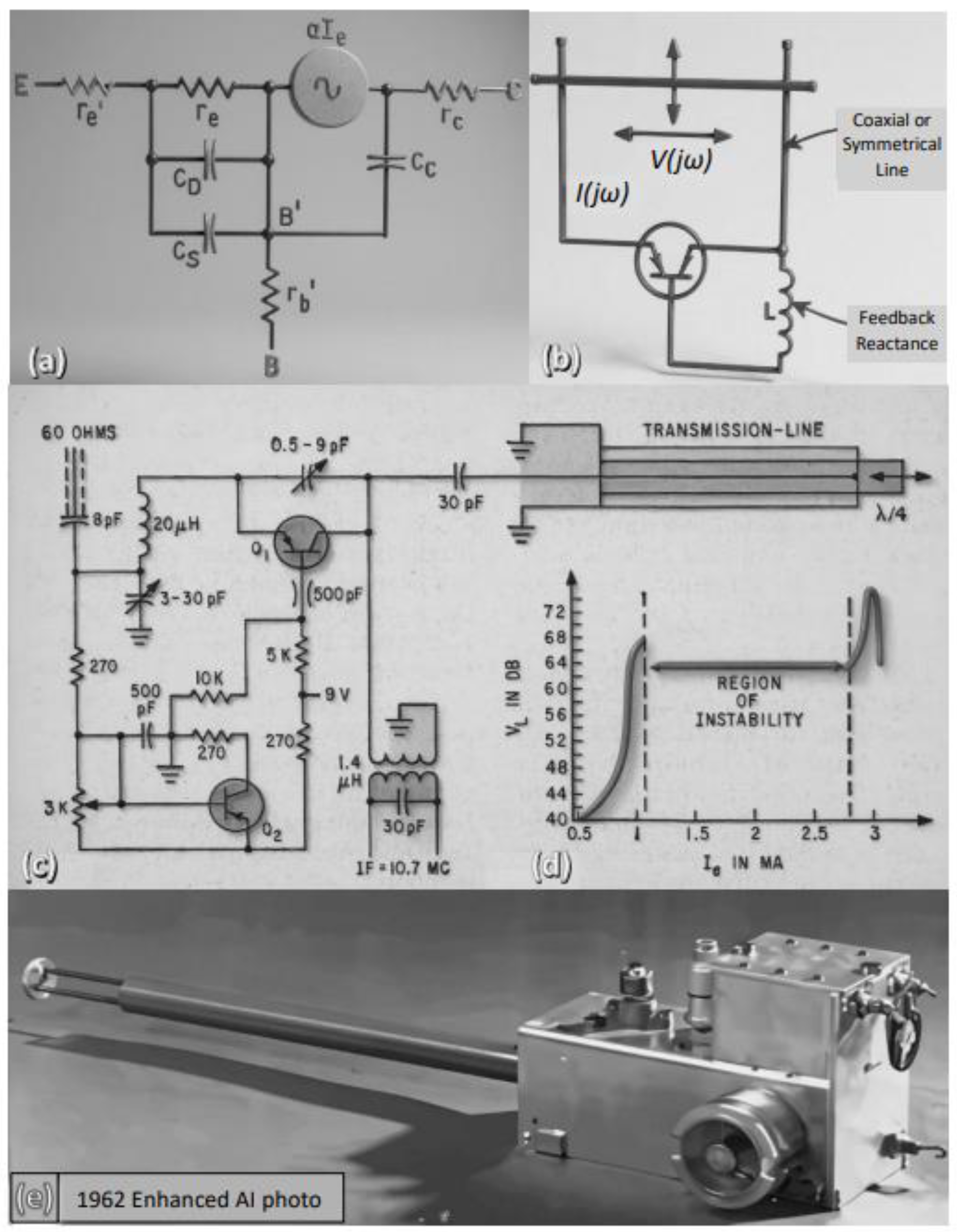
Figure 2.
Conceptual Examples of massive consumer products based on the emerging parametric geometric meta-electronics: True color TVs (A) and Cameras (B) operating by tunable detection and generation using meta-transistors in their pixel array structure with very fine frequency (or wavelength) tuning. Green energy harvester such as transparent solar panels (C) that can convert energy from all solar spectrum (D) into electricity with highly unexpected conversion efficiency unlimited by the semiconductor bandgap constrains. Photonics neural network (E) operating like human brain and configured for different deep learning methods such as reinforcement, supervised, or unsupervised learning. Finaly, quantum processors (F) and quantum memory are possible to build quantum computers based on superconductor meta-transistors operating at room temperature. (A, B, C, D, E, and F, are humanized AI generated images with fully paid service).
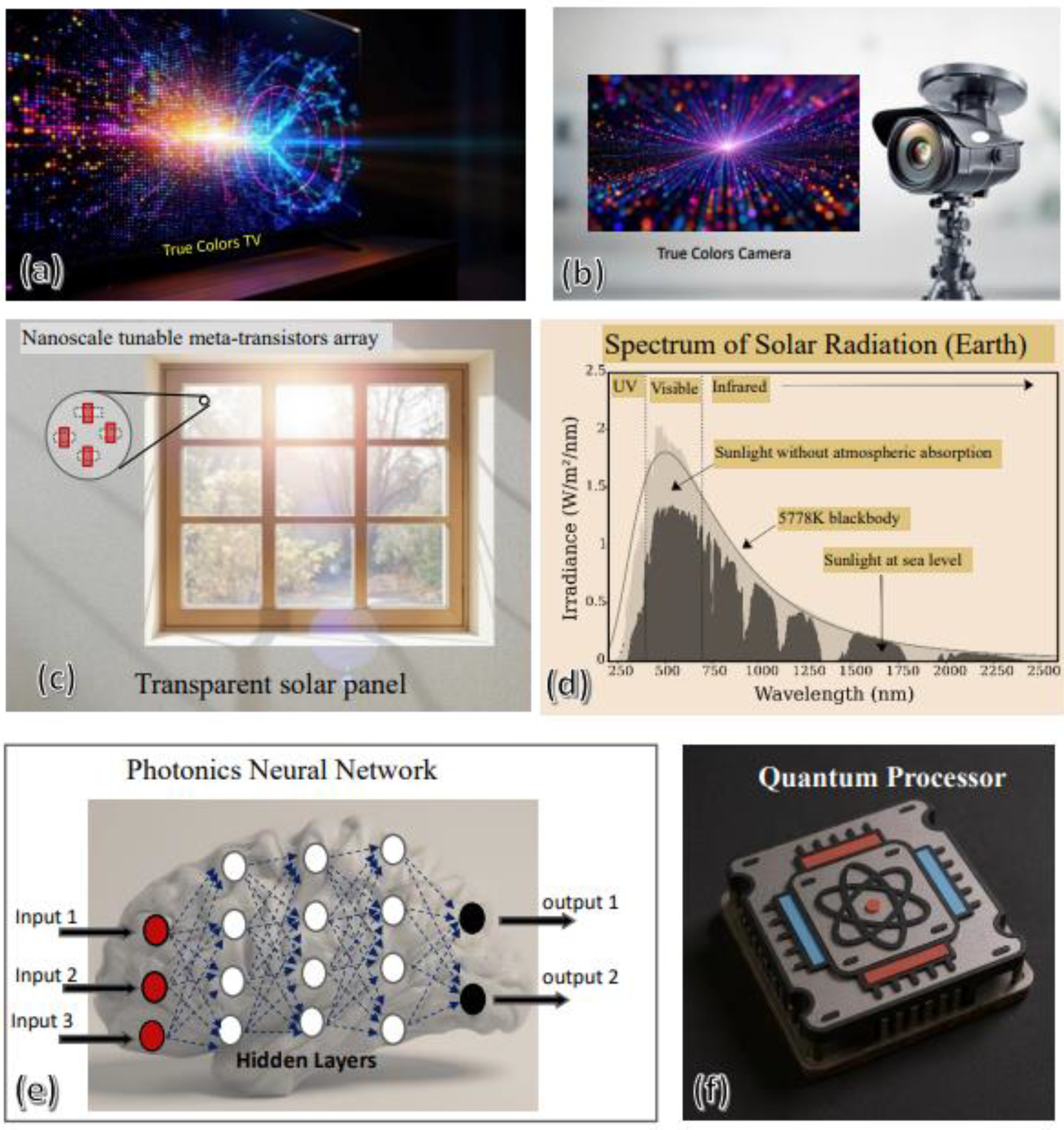
Figure 3.
Equivalent circuit of a flux-driven Josephson Parametric Amplifier (JPA) consisting of λ/4 coplanar resonator terminated by a SQUID (A). The inductance of the SQUID is controlled by the magnetic flux bias which is induced by the bias current (Ib) and modulated by the pump signal at twice the frequency of the signal to parametrically amplify the input signal. 3D visualization of possible dc-SQUID element (B) using two Josephson junctions between two superconductor wires. (A, after Yamamoto et al. Ref. 23, © 2008 APL).
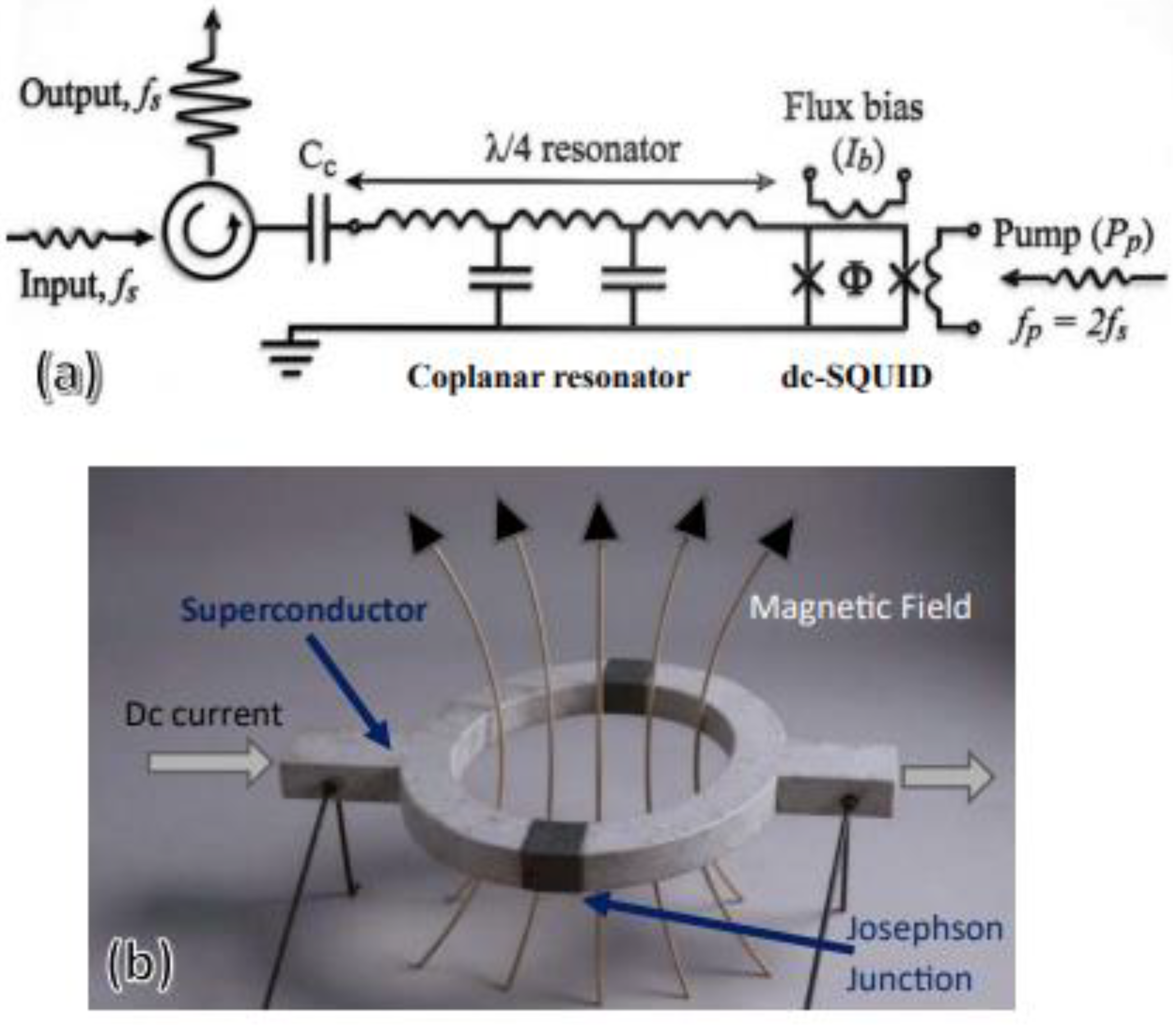
Figure 4.
A 2D cut of an N-channel MOSFET meta-device (A) with semitransparent Ti film, upon which a superimposed subwavelength diffraction grating gold metallization, the inversion layer size of the used MOSFET was 250μm x 250μm. Where ns is the inversion layer electron density, m* is the effective mass of the inversion layer electron, and 1/τ is the electron scattering rate. The measured fractional change in transmission ΔT/T is shown in (B) as dotted line and produced by conventional Fourier transform spectrometer at 1.2oK with resolution of 1cm-1. Solid curves are simple abstracted theoretical modeling of fractional change in far-infrared transmission with and without the diffraction grating. If real natural frequency resonance takes place in this experiment, the curve should demonstrate sharp peaks versus frequency with repetitive peaks of resonance harmonics as well. (A, B, after Allen et al, ref. 5, © 2008 PRL).
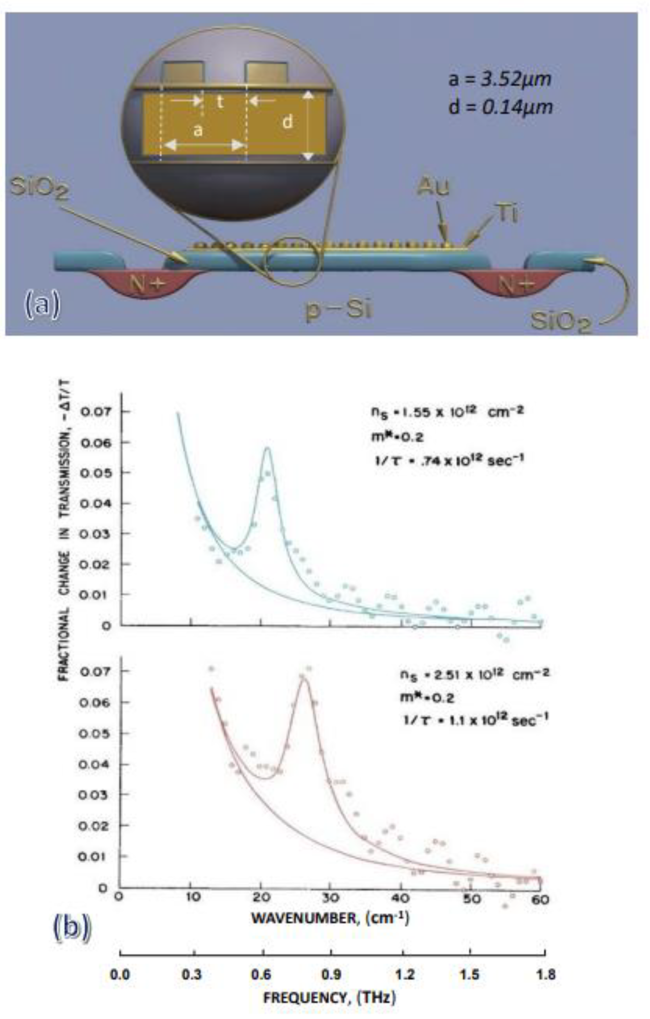
Figure 5.
A transmission line circuit model (A) for subwavelength 2DEG within the channel of FET taking into consideration the surrounding dielectric material. A Simple FET structure (B) showing the beyond saturation operation with part of the conducting carriers flow in a resistive channel and then flow in a fully depleted region with saturation velocity. A transmission line model of FET operating in the deep saturation region (C). The measured 0.2THz response of FETs (D) showing simultaneous broadband dc-rectifications and tunable dc-instability within the saturation regime operation. Broadband THz detection due to rectification of damped evanescent oscillations (E) at both source and drain sides of FETs. Tunable THz detection and generation due to quantum localized resonance oscillations (F) at only the drain side of FETs, (D after Elkhatib, ref. 19, © 2010 RPI).
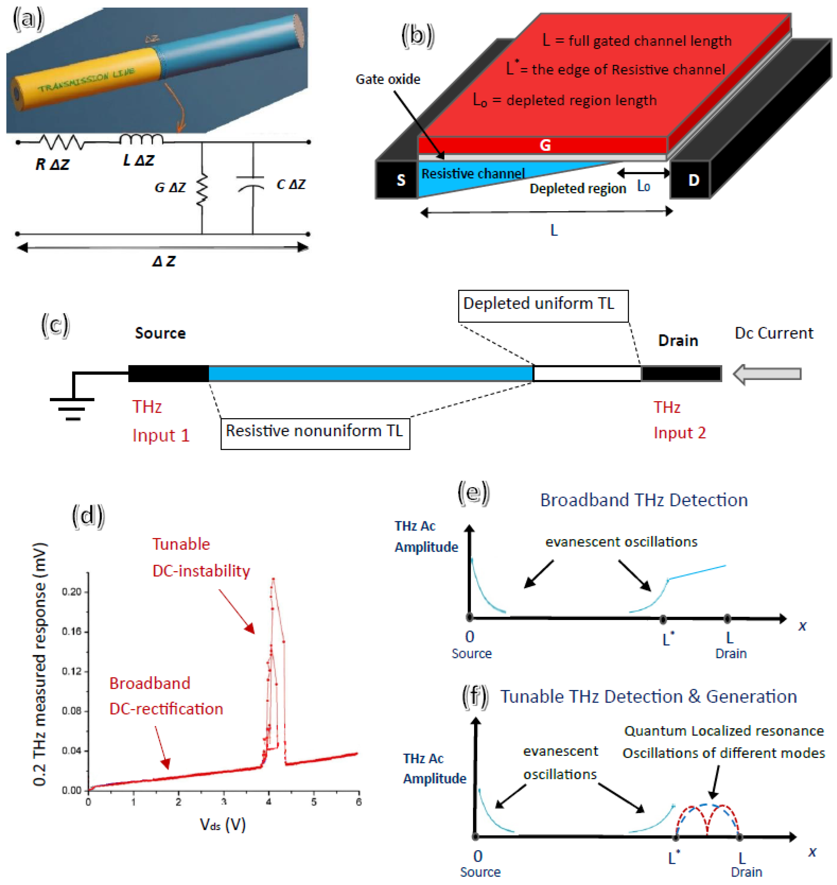
Figure 6.
The first three energy levels and wave-functions of a free electron of mass m confined in the depletion region of Length Lo at natural quantum localized resonance oscillations. The energy levels are labelled according to the quantum number n, which gives the number of half wavelengths in the wavefunction solution of Schrödinger equation with prober boundary conditions. (after Kittel, ref. 26, © 2005 John Wiley & Sons).
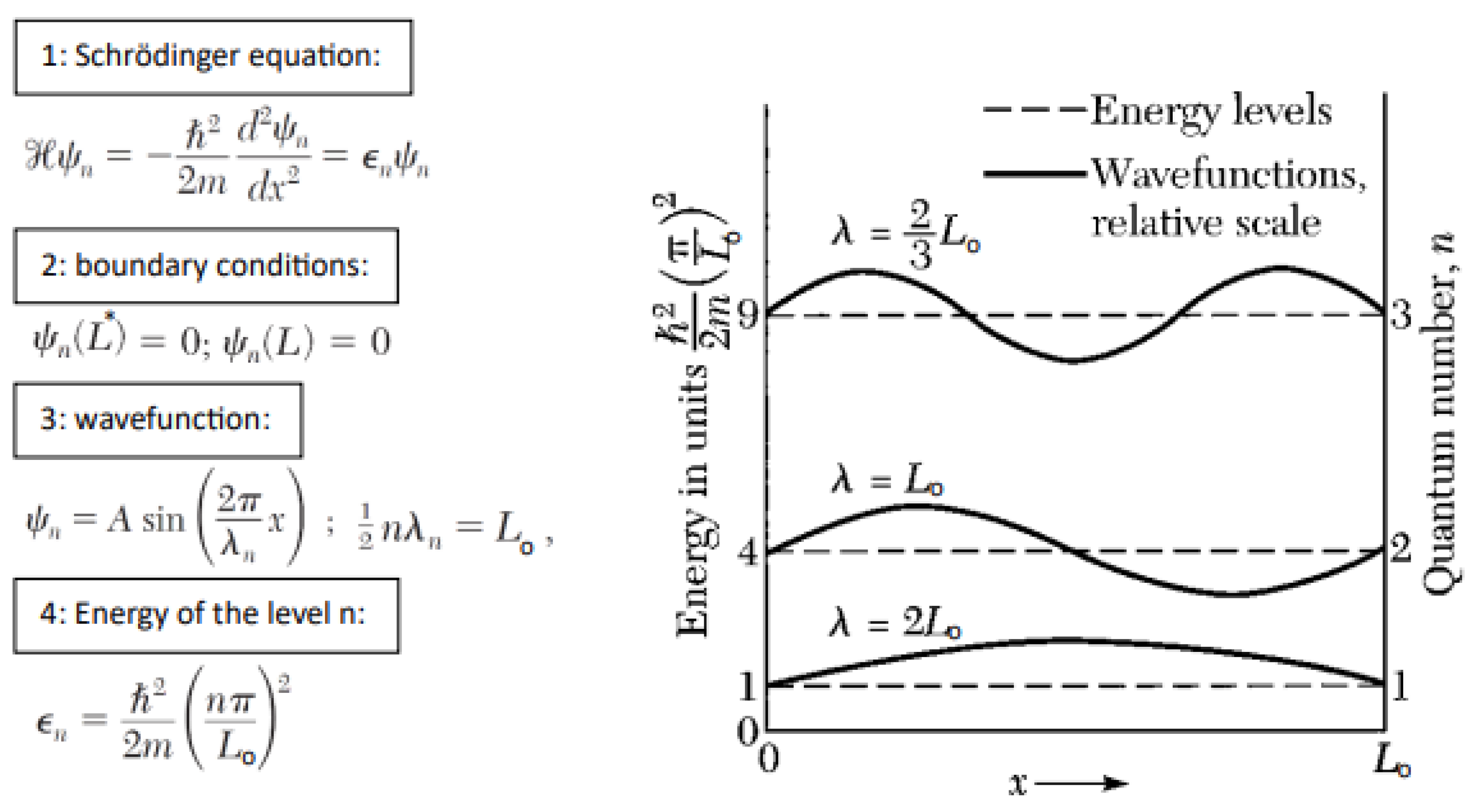
Figure 7.
Stabilizing the uncontrolled amplifications of quantum localized resonance oscillations causing the dc instability of transistor current using different feedback electronics circuit principles such as: the differential pair, VCO, ring oscillators (A), the LC differential crossed-coupled oscillator (B) with additional tail current source to lower supply sensitivity, the single transistor Colpitts oscillator (C) with feedback capacitance between transistor’s drain and source terminals. (A, B, and C, After Razavi, ref. 21, © 2001 McGraw Hill).

Disclaimer/Publisher’s Note: The statements, opinions and data contained in all publications are solely those of the individual author(s) and contributor(s) and not of MDPI and/or the editor(s). MDPI and/or the editor(s) disclaim responsibility for any injury to people or property resulting from any ideas, methods, instructions or products referred to in the content. |
© 2025 by the authors. Licensee MDPI, Basel, Switzerland. This article is an open access article distributed under the terms and conditions of the Creative Commons Attribution (CC BY) license (http://creativecommons.org/licenses/by/4.0/).
Copyright: This open access article is published under a Creative Commons CC BY 4.0 license, which permit the free download, distribution, and reuse, provided that the author and preprint are cited in any reuse.


