Submitted:
24 July 2025
Posted:
25 July 2025
You are already at the latest version
Abstract
Hollow coaxial double-shell submicron fibers were fabricated by combining electrospinning and atomic layer deposition (ALD). Polyvinyl alcohol (PVA) fibers were electrospun to serve as templates for the subsequent atomic layer deposition (ALD) of ZnO doped with transition metals (TM: Ni, Co, and Fe). An inner shell of amorphous Al₂O₃ was first deposited at low-temperature ALD to protect the polymer template. The PVA core was then removed through high-temperature annealing in air. Finally, a top shell of TM-doped ZnO was deposited at an elevated temperature within the ALD window for ZnO. The morphology, microstructure, elemental composition, and crystallinity of these submicron hollow double-shell fibers were thoroughly investigated using scanning electron microscopy (SEM), energy-dispersive X-ray spectroscopy (EDX), X-ray diffraction (XRD), and X-ray photoelectron spectroscopy (XPS).
Keywords:
submicron hollow fibers
; electrospinning
; atomic layer deposition (ALD)
; transition metal oxide (TMO)
1. Introduction
The field of nanomaterials and nanotechnology holds significant importance in contemporary scientific investigations. These materials find applications across various aspects of life, while their practical performance is determined by their nanostructural architecture and the constituent materials.
The partially filled d-orbitals of transition metal ions and the high electronegativity of oxygen atoms in transition metal oxides (TMOs) account for their intriguing and diverse properties, making them a widely investigated class of materials. These unique electronic structures are manifested in a range of phenomena, including colossal magnetoresistance (CMR), high-temperature superconductivity, electrocatalytic and photocatalytic activity, as well as ferromagnetic, ferroelectric, ferroelastic, thermoelectric, multiferroic, and gas-sensing capabilities [1,2,3,4,5,6].
The nanomaterials are a class of materials characterized by having at least one dimension in the range of 1 to 100 nm. Based on the number of nanosized dimensions, the architecture of nanomaterials can be categorized into four main groups: 0D (nanoparticles, quantum dots); 1D (nanorods, nanowires, nanofibers); 2D (nanosheets, graphene, other 2D materials); and 3D (nanospheres, nanoprisms, nanotubes, nanoporous materials). Two primary approaches exist for the production of diverse nanomaterials: top-down and bottom-up. The top-down approach is a subtractive method involving the breakdown of a bulk material into nanomaterials (e.g., nanolithography, mechanical milling, laser ablation, sputtering, electron explosion, arc discharge, electrospinning, and thermal decomposition). In contrast, the bottom-up approach entails the assembly of nanostructures from atomic or molecular precursors through methods, such as chemical vapor deposition (CVD), atomic layer deposition (ALD), sol-gel processing, spin coating, and pyrolysis [7,8,9].
Nanotubular fibers represent a promising class of three-dimensional (3D) nanomaterials for applications in batteries, catalysis, and gas sensing, primarily due to their high specific surface area. Several fabrication methods have been developed, among which electrospinning is particularly versatile. This technique encompasses configurations, such as single-nozzle, coaxial, triaxial, microfluidic, and emulsion electrospinning, along with hybrid approaches that integrate electrospinning and atomic layer deposition [10,11,12,13,14].
Numerous research groups have utilized a combination of electrospinning and ALD to fabricate various fiber structures. In the conventional approach, a low-temperature ALD process is employed following electrospinning to coat the polymer fibers with different thin films, thereby preventing polymer degradation. However, at these reduced temperatures, some deposited films exhibit non-ideal, non-self-limiting growth behaviour, as the process often operates outside the optimal ALD temperature window. Furthermore, in certain cases, post-deposition annealing of such structures can induce the Kirkendall effect, resulting in the disruption of the microtubular morphology [15].
To overcome these challenges, we adopted a modified approach. First, the polymer fibers were coated with Al₂O₃ via low-temperature ALD. Owing to its thermal and chemical stability, Al₂O₃ acts as an inert structural matrix. Subsequent thermal annealing was performed to obtain hollow Al₂O₃ fibers. This sequence enabled the final deposition of desired functional active films by thermal ALD, ensuring growth within their respective optimal ALD windows.
In this study, two-layered hollow submicron fibers were produced by combining electrospinning and ALD. The inner shell consisted of amorphous Al₂O₃, while the outer shell was ZnO doped with Co, Fe, or Ni. The morphology and elemental composition of the resulting hollow double-shell fibers were investigated using scanning electron microscopy (SEM) coupled with energy dispersive X-ray (EDX) spectroscopy. The crystalline structure was analyzed by X-ray diffraction (XRD), and the surface chemical states and elemental composition were determined using X-ray photoelectron spectroscopy (XPS) analysis.
2. Materials and Methods
2.1. Sample Preparation Method
ZnO:TM/Al₂O₃ hollow fibers were fabricated using a combination of electrospinning and atomic layer deposition (ALD), where TM represents the transition metals cobalt (Co), iron (Fe), or nickel (Ni), and ALO refers to aluminum oxide (Al₂O₃). The synthesis followed a previously established multi-step procedure [15]: electrospinning of a polyvinyl alcohol (PVA) polymer, low-temperature ALD of Al₂O₃, high-temperature annealing for the removal of the PVA template, and thermal ALD of ZnO doped with the respective transition metal. Detailed parameters and procedures for each of these techniques are provided in the subsequent sections.
2.1.1. Electrospinning
Template fibers were fabricated using electrospinning from an 8-wt% aqueous solution of polyvinyl alcohol (PVA, VALERUS, 93.5% purity, 7200MW). This solution was prepared by continuous stirring at 60 ℃ until achieving the viscoelastic properties needed for electrospinning. For the electrospinning process, the PVA solution was loaded into a syringe fitted with a stainless-steel needle. It was then dispensed at a flow rate of 1 mL/hour within custom-built electrospinning equipment, where it was subjected to an electric field with a strength of 1.4 kV/cm at an ambient temperature of approximately 24 ℃. The resulting PVA fiber mat demonstrated good adhesion to the surface of flat glass substrates.
2.1.2. Low-Temperature ALD
Conformal amorphous aluminum oxide (Al2O3, ALO) films were deposited onto the PVA fibers using ALD within a Beneq TFS-200 reactor. A low deposition temperature of 60 ℃ was maintained to ensure the integrity of the polymer fibers. The ALD cycle involved a 300-ms pulse of trimethylaluminum (Al2(CH3)6, TMA) as the aluminum precursor, followed by a 5-s nitrogen (N2, 99.999% purity) purge. Subsequently, deionized water (DI H2O) was introduced as the oxygen precursor, also followed by a 5-s nitrogen purge. This sequence was repeated for 150 cycles to achieve the desired ALO film thickness.
2.1.3. High-Temperature Annealing
The polymer template was removed from the fiber structures by annealing in air using a Carbolite horizontal tube furnace equipped with a Eurotherm 3508 temperature controller. The thermal treatment consisted of a heating ramp from ambient temperature to 500 °C at a rate of 5 °C/min, followed by an isothermal dwell at 500 °C for 24 hours. Subsequently, the furnace was cooled to room temperature at the same controlled rate of 5 °C/min.
2.1.4. Thermal ALD
Following the successful synthesis of hollow Al₂O₃ (ALO) fibers, transition metal oxide (TMO) films were deposited at an elevated temperature within the optimal ALD window to ensure optimal stoichiometry and crystallinity. ZnO films doped with transition metals (TM) were deposited onto the ALO tubular fibers via ALD supercycles (Figure 1). Each supercycle comprised two subcycles: one for ZnO and one for TMO deposition. ZnO was deposited using sequential pulses of diethylzinc ((C₂H₅)₂Zn, DEZ) and deionized H₂O precursors, each with a 0.3-s pulse duration separated by a 5-s nitrogen purge. For TMO deposition, sequential 2-s pulses of metallocene ((C₅H₅)₂M, MeCp₂) and 1-s pulses of ozone (O₃) were utilized, separated by a 5-s nitrogen purge. The metallocenes employed were cobaltocene (Co(C₅H₅)₂, Cp₂Co), ferrocene (Fe(C₅H₅)₂, Cp₂Fe), or nickelocene (Ni(C₅H₅)₂, Cp₂Ni). These metallocene powder precursors, placed in a hot source (HS) container, required heating for evaporation. Due to the inherently low reaction rate of MeCp₂ with H₂O, ozone was selected as the oxidant instead of water, owing to its higher reactivity. To optimize the film deposition, two series of ZnO:TMO films were prepared with varying temperatures and cycle numbers (Table 1).
2.2. Sample Characterization Techniques
Comprehensive characterization of the microstructure, elemental composition, and crystallinity was performed on two series of double-layered tubular ZnO:TM/ALO fibers (TM = Co, Fe, or Ni) synthesized on glass substrates. These analyses employed scanning electron microscopy (SEM), energy-dispersive X-ray spectroscopy (EDX), X-ray diffraction (XRD), and X-ray photoelectron spectroscopy (XPS).
2.2.1. SEM and EDX
A JSM T 200 (Jeol, Akishima, Tokyo, Japan) and a TESCAN LYRA scanning electron microscopes (SEMs) were used to investigate the morphology of the films. Additionally, energy dispersive X-ray spectroscopy (EDX) carried out by a Bruker Quantax EDS detector provided identification and quantification of their elemental composition.
2.2.2. XRD
The X-ray diffraction study was performed on a Bruker D8 Advance Bragg-Brentano diffractometer equipped with a copper anode X-ray tube operated at 40 kV/40 mA and a LynxEye position-sensitive detector. The X-ray patterns were collected in the angular range 10 – 70o 2Θ with a step of 0.04o 2Θ and integrated total counting time of 4 s/step.
2.2.3. XPS
The X-ray photoelectron spectra were obtained using achromatic Al Kα (1486.6 eV) radiation in a VG ESCALAB MK II electron spectrometer under base pressure of 1×10⁻⁸ Pa. The spectrometer resolution was calculated from the Ag3d5/2 line with an analyzer transmission energy of 20 eV. The full width at half maximum (FWHM) of this line was 1 eV. The spectrometer was calibrated against the Au4f7/2 line (84.0 eV) and the samples charging was estimated from C1s (285 eV) spectra from natural hydrocarbon contamination on the surface. The accuracy of the BE measured was 0.2 eV. The photoelectron spectra of C1s, O1s, Al2p, Zn2p and Co2p, Fe2p and Ni2p were recorded and corrected by subtracting a Shirley-type background and quantified using the peak area and Scofield’s photoionization cross-sections.
3. Results and Discussions
High-quality double-layered hollow ZnO:TM/ALO fibers were successfully synthesized; they exhibited uniform distribution, well-defined shapes, and smooth, defect-free surfaces (Figure 2). The fiber thickness and fiber-wall thickness were directly determined from SEM images, with these findings corroborated by ellipsometry measurements on films deposited on p-Si(100) reference substrates. (the ellipsometry consistently showed 2-3 nm thinner films, likely due to a slower initial reaction rate on Si compared to the HO-rich PVA surface.)
The outer fiber diameters varied from 310 to 420 nm depending on the ALD regime (Table 1 and Table 2). Due to shrinkage occurring during the ALD and annealing processes, in some cases the resulting ZnO/Al₂O₃ fibers possessed smaller diameters than the initial pure PVA fibers [15]. Notably, the pure ZnO/ALO and ZnO:Ni/ALO fibers in both series (s1 and s2) displayed larger diameters. The increased diameter in ZnO/ALO-s1 is attributed to the higher number of ZnO ALD cycles compared to its doped counterparts (Table 1). Significantly, the ZnO:Ni/ALO-s1 was the only sample in its series where nickel (Ni) was detected via EDX and XPS analysis (see below). This observation suggests a faster reaction kinetic for nickelocene compared to ferrocene and cobaltocene within this specific ALD regime. ALD regime for series 2 is distinguished by more TMO cycles and higher precursor and reactor temperatures. Increasing the temperatures accelerates the kinetic reaction of metallocenes and ozone and, therefore, Ni and Fe dopants are detected in this series. On the other hand, the higher temperature reduces the ZnO growth rate, since it is moved outside the ALD window [16,17,18,19].
The thickness of the fiber walls, i.e., the ZnO:TM/ALO films, was determined from SEM images (Figure 3, Table 2) as well as from ellipsometry measurements performed on the same films deposited on p-Si(100) reference substrates. Both methods yielded comparable wall thicknesses between 60 to 140 nm. The wall thickness variation within each series is attributed to differences in the initial growth rate.
It should be noted that the Ni-doped ZnO fibers exhibit a clearly visible grain structure with mean grain diameters of approximately 50 nm (Figure 3 (c)-(e)). Furthermore, in some samples, Series 2, clogged fibers were observed (Figure 3(e)). This is attributed to the non-self-limiting ALD regime in Series 2, which results in a mixed CVD-ALD growth for ZnO and, consequently, the occlusion of some hollow fibers.
Figure 4 presents an EDX analysis of ZnO:TM/ALO-s2 hollow fibers fabricated on glass substrates. In all samples, zinc (Zn) and aluminum (Al), originating from the ZnO/Al₂O₃ fibers, are clearly visible. Given the fibrous mesh structure, elements from the underlying glass substrate, such as calcium (Ca), silicon (Si), and magnesium (Mg), are also detectable. For the doped fibers, nickel (Ni) and iron (Fe) elements are clearly observed. However, cobalt (Co) could not be detected in either series, which may be attributed to its concentration falling below the detection limit of the analysis.
The X-ray diffraction (XRD) analyses shown in Figure 5 revealed a polycrystalline hexagonal phase with a wurtzite-type structure for the ZnO:TM top shell of the hollow ZnO:TM/ALO fibers obtained. Table 3 summarizes the corresponding ZnO crystallite sizes. During ALD, sequential layers of ZnO and TMO were deposited. This growth mechanism, which depends on the reactor temperature (Figure 1), significantly influences the nanostructure of the resulting films. Pure and Ni-doped ZnO samples from Series 1 exhibit a strong, predominantly c-axis-oriented crystal structure and the largest crystallite sizes. Under regime 1, a reactor temperature of 200 °C provides an indispensable ALD window, resulting in relatively smooth and conformal ZnO films. Conversely, at an elevated temperature (230 ℃), which is outside the optimal ALD window for ZnO, the growth mechanism transitions from pure ALD to a mixed CVD-ALD regime. This transition results in highly uneven coatings with decreased ZnO crystallinity – the ZnO/ALO and ZnO:Co/ALO films reveal no significant crystallization. On such surfaces, an increased density of initial growth points leads to a larger number of crystallites but, simultaneously, a reduced overall size. For the Ni-doped ZnO fiber structures, continuous nickel oxide sublayers were obtained in both ALD regimes (as observed in the XPS analysis below, Figure 8), which slightly affected the crystallographic orientation and size of the crystallites. At lower deposition temperatures, in the Co- and Fe-doped ZnO fiber structures, the reaction between metallocene and ozone proceeds very slowly or is even absent, leading to the formation of numerous defects that impair the crystal structure. As the temperature is raised, the reaction of ferrocene and ozone accelerates, enabling the formation of iron oxide sublayers and a corresponding increase in crystallite sizes. In these specific structures, an increase in the ab-oriented growth of ZnO is observed.
The XPS analysis detected the presence of C1s, O1s, and Zn2p signals on the surface of the ZnO:TM/ALO fiber structures. No Al2p signal was detected, primarily because XPS is a surface-sensitive technique with a typical X-ray penetration depth of only 3-5 nm. The observed C1s signal is attributed solely to surface contamination [15]. Notably, only nickel (Ni) and iron (Fe) were detected as doping elements (further explanation provided below). In the Zn2p region, zinc appeared as a characteristic doublet, Zn2p3/2 and Zn2p1/2, with a spin-orbit splitting of 23.1 eV, consistent with ZnO (Figure 6).
The O1s photoelectron line, centered at approximately 530.0 eV, is characteristic of oxygen within metal oxides. A smaller shoulder at the higher binding energy of 531.5 eV was consistently observed across all studied samples (Figure 7), which is attributed to the formation of oxygen vacancies in the ZnO lattice [20]. Consequently, the O1s photoelectron spectra provide valuable insights into the changes occurring in ZnO after doping with Co, Fe, or Ni. For ZnO doped with Co, Fe, and Ni at a lower ALD deposition temperature (Series 1), a slight increase in the oxygen vacancy formation was observed compared to the pure ZnO fibers deposited under the same conditions. At this deposition temperature, only Ni was identifiable as a dopant in the Ni2p region. The fibers deposited at higher temperatures exhibited a lower concentration of oxygen vacancies. Doping pure ZnO with Co, Fe, and Ni again resulted in modifications in the number of oxygen vacancies. Specifically, Co and Fe doping of ZnO reduced the oxygen vacancies, while Ni doping caused an increase. It's important to note that in this higher temperature ALD regime (Series 2), only Fe and Ni were detected on the surface of the studied fibers. Overall, ZnO and Co, Fe, and Ni-doped ZnO deposited at higher temperatures and with more cycles exhibited a lower number of oxygen vacancies than those deposited at lower temperatures and with fewer cycles.
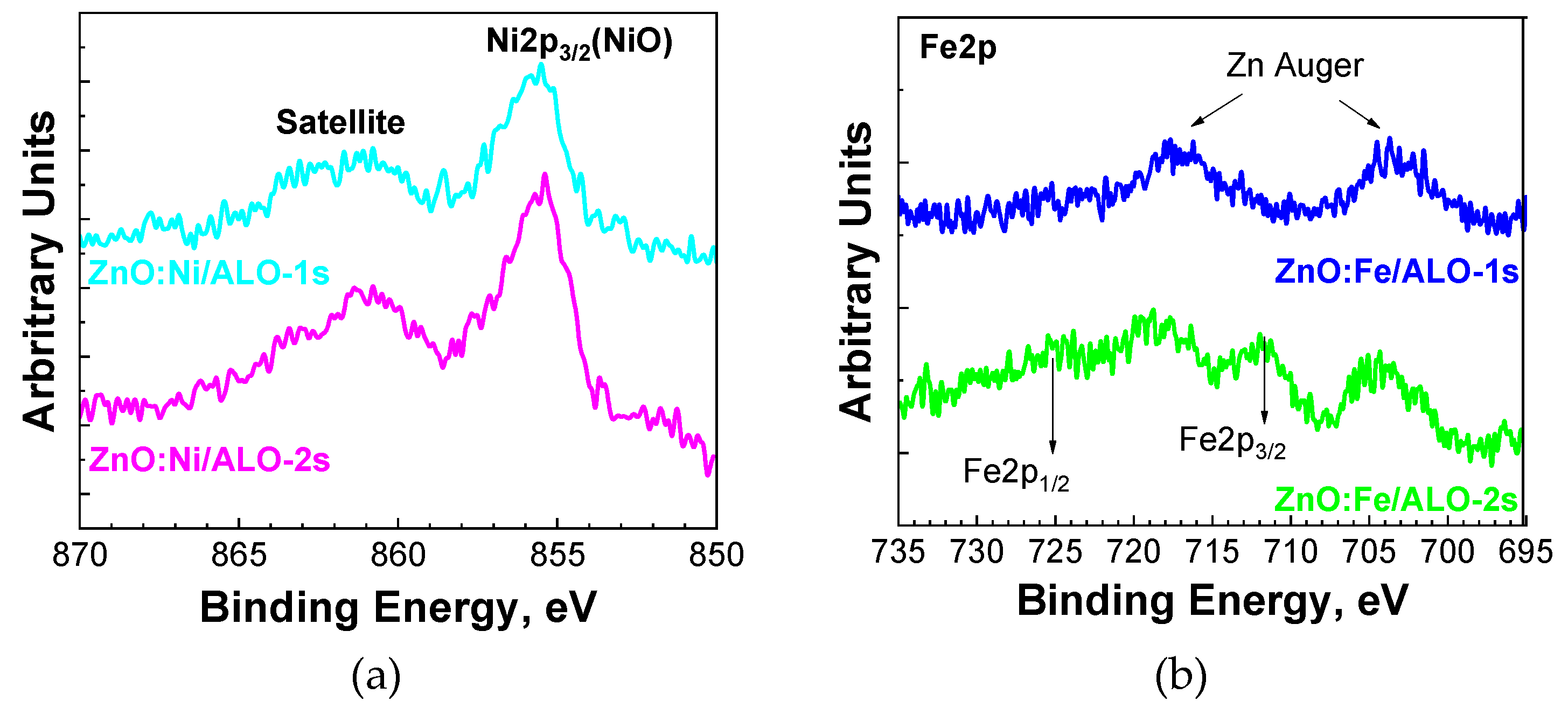
The Ni2p core-level spectra for both deposition temperatures show nickel in a Ni²⁺ oxidation state around 855.5 eV consistent with the presence of NiO or Ni(OH)₂ (Figure 8a) [21]. Conversely, iron (Fe) was detected only in the sample prepared at the higher deposition temperature (Series 2). The Fe2p signal overlaps significantly with the Zn Auger peaks (Figure 8b), making the precise determination of the Fe2p peak positions challenging. Nevertheless, the Fe2p3/2 peak is discernible between the Zn Auger peaks at approximately 712 eV for ZnO:Fe/ALO-2s fibers. Due to the close binding energies of Fe²⁺ and Fe³⁺ oxidation states in various iron oxides (Fe₂O₃, Fe₃O₄, FeO, and FeO(OH)) [22] and the overlap observed, identifying precisely the specific type of iron oxide in this study proved difficult.
Figure 8.
XPS of Ni2p3/2 (a) and Fe2p (b) of ZnO:TM/ALO fibers.
4. Conclusions
We report on the successful fabrication of submicron tubular double-shell ZnO:TM/Al₂O₃ (TM – Ni and Fe) fibers on glass substrates achieved through a synergistic approach integrating electrospinning, atomic layer deposition (ALD), and high-temperature annealing. The SEM imaging analysis confirmed the formation of these structures. The crystallographic analysis study revealed that ZnO primarily grew with a c-axis orientation at 200 °C, a regime in which only Ni dopant was incorporated. Increasing the deposition temperature to 230 °C and the number of TMO cycles induced additional crystalline orientations in ZnO and promoted crystallite growth, indicating a transition to a mixed ALD-CVD growth mechanism. Crucially, these optimized high-temperature conditions facilitated the effective incorporation of both Ni and Fe dopants, detectable by EDX and XPS. The ability to precisely control the electrospinning, the ALD, and the annealing parameters enabled the production of TMO hollow fibers with customizable features. Given their high specific surface area and tunable TMO composition, these 3D nanostructures are highly promising for advanced gas-sensing applications.
Author Contributions
Conceptualization, B.S.B. and B.G.; methodology, B.S.B., B.G., K.S., N.S., K.B., V.M., L.S., D.S. and A.P.; validation, B.S.B. and B.G.; formal analysis, B.S.B. and B.G., investigation, B.S.B., B.G., I.A., P.T. (Peter Tzvetkov), K.S., N.S., K.B., V.M., L.S., P.T. (Penka Terziyska), D.S. and A.P.; resources, B.S.B.; data curation, B.S.B. and B.G.; writing—original draft preparation, B.S.B. and B.G.; writing—review and editing, B.S.B., B.G., I.A., P.T. (Peter Tzvetkov), and A.P.; visualization, B.S.B. and B.G.; supervision, B.S.B.; project administration, B.S.B.; funding acquisition, B.S.B. All authors have read and agreed to the published version of the manuscript.
Funding
This work has been financially supported by the Bulgarian National Scientific Fund, Project КP-06-Н88/7.
Institutional Review Board Statement
Not applicable.
Informed Consent Statement
Not applicable.
Data Availability Statement
The datasets that support the findings in this study are available from the corresponding author upon reasonable request.
Acknowledgments
The authors acknowledge the financial support provided by the Bulgarian National Science Fund under Project KP-06-Н88/7. We also extend our sincere gratitude to Chavdar Ghelev (Institute of Electronics, Bulgarian Academy of Sciences) for his valuable assistance and constructive comments, which have significantly contributed to the development of this work.
Conflicts of Interest
The authors declare no conflict of interest.
References
- Sahoo, S.; Wickramathilaka, K.Y.; Njeri, E.; Silva, D.; Suib, S.L. A review on transition metal oxides in catalysis. Front. Chem. 2024, 12, 1374878. [Google Scholar] [CrossRef]
- Goodenough, J.B. A Perspective on Engineering Transition-Metal Oxides. Chem. Mater. 2013, 26, 820–829. [Google Scholar] [CrossRef]
- Lany, S. Semiconducting transition metal oxides. J. Phys.: Condens. Matter. 2015, 27, 283203. [Google Scholar] [CrossRef]
- Rao, C.N.R. Transition metal oxides. Annu. Rev. Phys. Chem. 1989, 40, 291. [Google Scholar] [CrossRef]
- Tokura, Y.; Nagaosa, N. Orbital physics in transition-metal oxide. Science 2000, 288, 462. [Google Scholar] [CrossRef]
- Sun, Z.; Liao, T.; Dou, Y.; Hwang, S.M.; Park, M-S. ; Jiang, L.; Kim, J.H.; Dou, S.X. Generalized self-assembly of scalable two-dimensional transition metal oxide nanosheets. Nat. Commun. 2014, 5, 3813. [Google Scholar] [CrossRef]
- Baig, N.; Kammakakam, I.; Falath, W. Nanomaterials: a review of synthesis methods, properties, recent progress, and challenges. Mater. Adv. 2021, 2, 1821. [Google Scholar] [CrossRef]
- Byakodi, M.; Shrikrishna, N.S.; Sharma, R.; Bhansali, S.; Mishra, Y.; Kaushik, A.; Gandhi, S. Emerging 0D, 1D, 2D, and 3D nanostructures for efficient point-of-care biosensing. Biosensors and Bioelectronics 2022, 12, 100284. [Google Scholar] [CrossRef] [PubMed]
- Mekuye, B.; Abera, B. Nanomaterials: An overview of synthesis, classification, characterization, and applications. Nano Select 2023, 4, 486. [Google Scholar] [CrossRef]
- Xia, X.; Dong, X.J.; Wei, Q.F.; Cai, Y.B.; Lu, K.Y. Formation mechanism of porous hollow SnO2 nanofibers prepared by one-step electrospinning. Express Polym. Lett. 2012, 6, 169. [Google Scholar] [CrossRef]
- Lu, Z.; Zhou, Q.; Wei, Z.; Xu, L.; Peng, S.; Zeng, W. Synthesis of Hollow Nanofibers and Application on Detecting SF6 Decomposing Products. Front. Mater. 2019, 6, 183. [Google Scholar] [CrossRef]
- Kim, W-S. ; Lee, B-S.; Kim, D-H.; Kim, H-C.; Yu, W-R.; Hong, S-H. SnO2 nanotubes fabricated using electrospinning and atomic layer deposition and their gas sensing performance. Nanotechnology 2010, 21, 245605. [Google Scholar] [CrossRef] [PubMed]
- Li, L.; Peng, S.; Lee, J.K.Y.; Ji, D.; Srinivasan, M.; Ramakrishna, S. Electrospun hollow nanofibers for advanced secondary batteries. Nano Energy 2017, 39, 111. [Google Scholar] [CrossRef]
- Homaeigohar, S.; Davoudpour, Y.; Habibi, Y.; Elbahri, M. The Electrospun Ceramic Hollow Nanofibers. Nanomaterials 2017, 7, 383. [Google Scholar] [CrossRef]
- Blagoev, B.S.; Georgieva, B.; Starbova, K.; Starbov, N.; Avramova, I.; Buchkov, K.; Tzvetkov, P.; Stoykov, R.; Terziyska, P.; Delibaltov, D.; Mehandzhiev, V.; Paskaleva, A. A Novel Approach to Obtaining Metal Oxide HAR Nanostructures by Electrospinning and ALD. Materials 2023, 16, 7489. [Google Scholar] [CrossRef]
- Guziewicz, E.; Godlewski, M.; Wachnicki, L.; Krajewski, T.A.; Luka, G.; Gieraltowska, S.; Jakiela, R.; Stonert, A.; Lisowski, W.; Krawczyk, M.; Sobczak, J.W.; Jablonski. A. ALD grown zinc oxide with controllable electrical properties. Semicond. Sci. Technol. 2012, 27, 074011. [Google Scholar] [CrossRef]
- Tapily, K.; Gu, D.; Baumgart, H.; Namkoong, G.; Stegall, D.; Elmustafa, A.A. Mechanical and structural characterization of atomic layer deposition-based ZnO films. Semicond. Sci. Technol. 2011, 26, 115005. [Google Scholar] [CrossRef]
- Janocha, E.; Pettenkofer, C. ALD of ZnO using diethylzinc as metal-precursor and oxygen as oxidizing agent. Appl. Surf. Sci. 2011, 257, 10031. [Google Scholar] [CrossRef]
- Xia, B.; Ganem, J.J.; Briand, E.; Steydli, S.; Tancrez, H.; Vickridge, I. The carbon and hydrogen contents in ALD-grown ZnO films define a narrow ALD temperature window. Vacuum, 2021, 190, 110289. [Google Scholar] [CrossRef]
- Park, S.-M.; Ikegami, T.; Ebihara, K. Effects of substrate temperature on the properties of Ga-doped ZnO by pulsed laser deposition. Thin Solid Films 2006, 513, 90. [Google Scholar] [CrossRef]
- Chen, J.; Dai, R.; Ma, H.; Lin, Z.; Li, Y.; Xi, B. Atomic Layer Deposition of Nickel Oxides as Electrocatalyst for Oxygen Evolution Reaction. Nanomaterials 2025, 15, 474. [Google Scholar] [CrossRef] [PubMed]
- Yamashita, T.; Hayes, P. Analysis of XPS spectra of Fe2+ and Fe3+ ions in oxide materials. Applied Surface Science 2008, 254, 2441. [Google Scholar] [CrossRef]
Figure 1.
ALD supercycle.
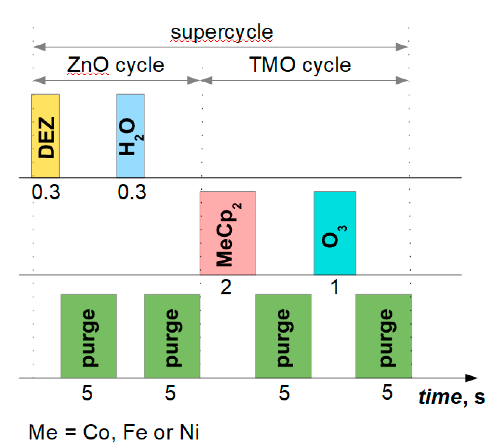
Figure 2.
SEM images of pure PVA fibers (a) and ZnO:TM/ALO fibers of Series 1, where TM is Co (b), Fe (c) and Ni (d).
Figure 2.
SEM images of pure PVA fibers (a) and ZnO:TM/ALO fibers of Series 1, where TM is Co (b), Fe (c) and Ni (d).
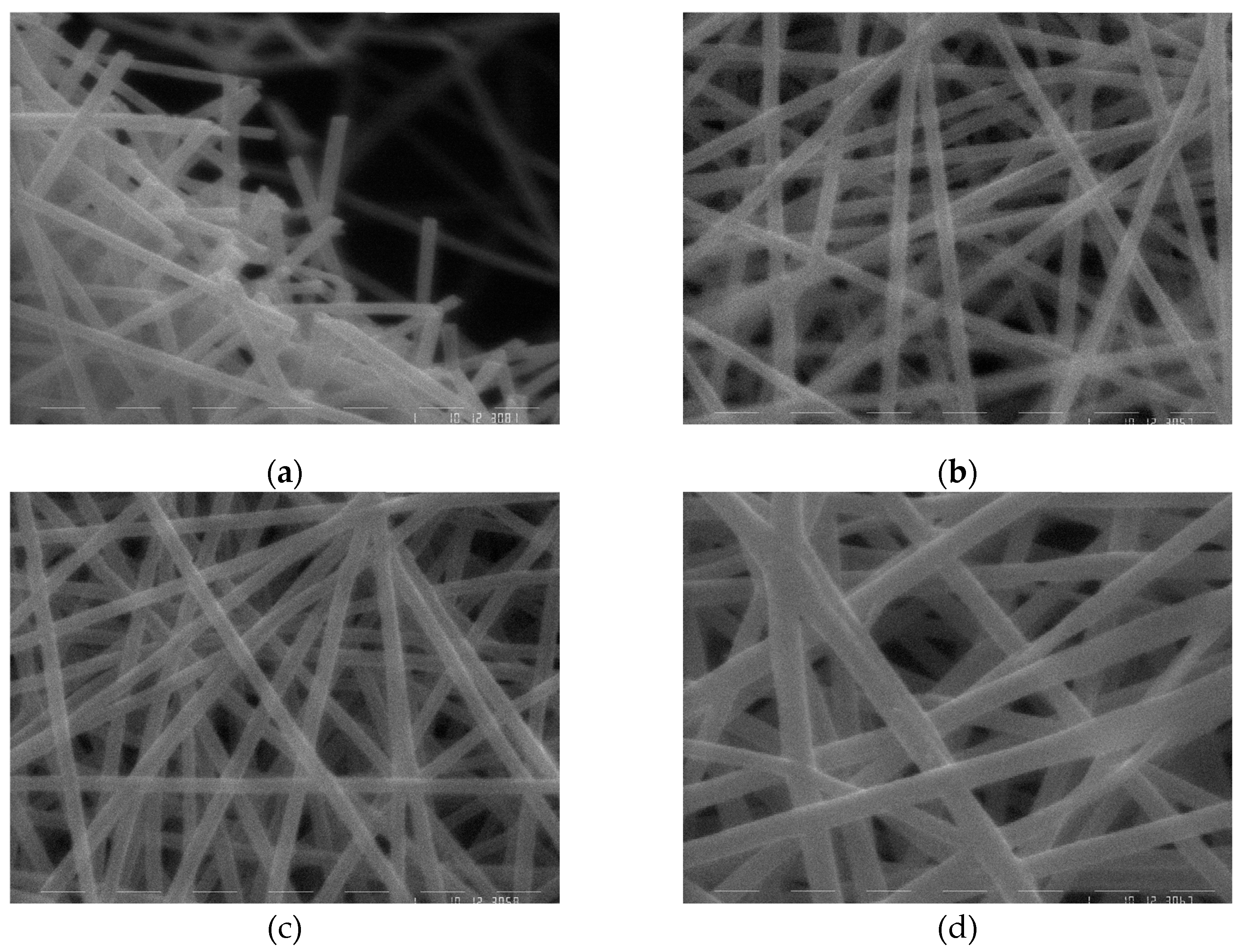
Figure 3.
SEM images of ZnO:Co/ALO (a), ZnO/ALO (b) and ZnO:Ni/ALO (c, d) fibers of Series 1; ZnO:Ni/ALO (e) and ZnO:Fe/ALO (f) fibers of Series 2.
Figure 3.
SEM images of ZnO:Co/ALO (a), ZnO/ALO (b) and ZnO:Ni/ALO (c, d) fibers of Series 1; ZnO:Ni/ALO (e) and ZnO:Fe/ALO (f) fibers of Series 2.
Figure 4.
EDX analysis of ZnO:TM/ALO-s2 hollow fibers on glass substrates.
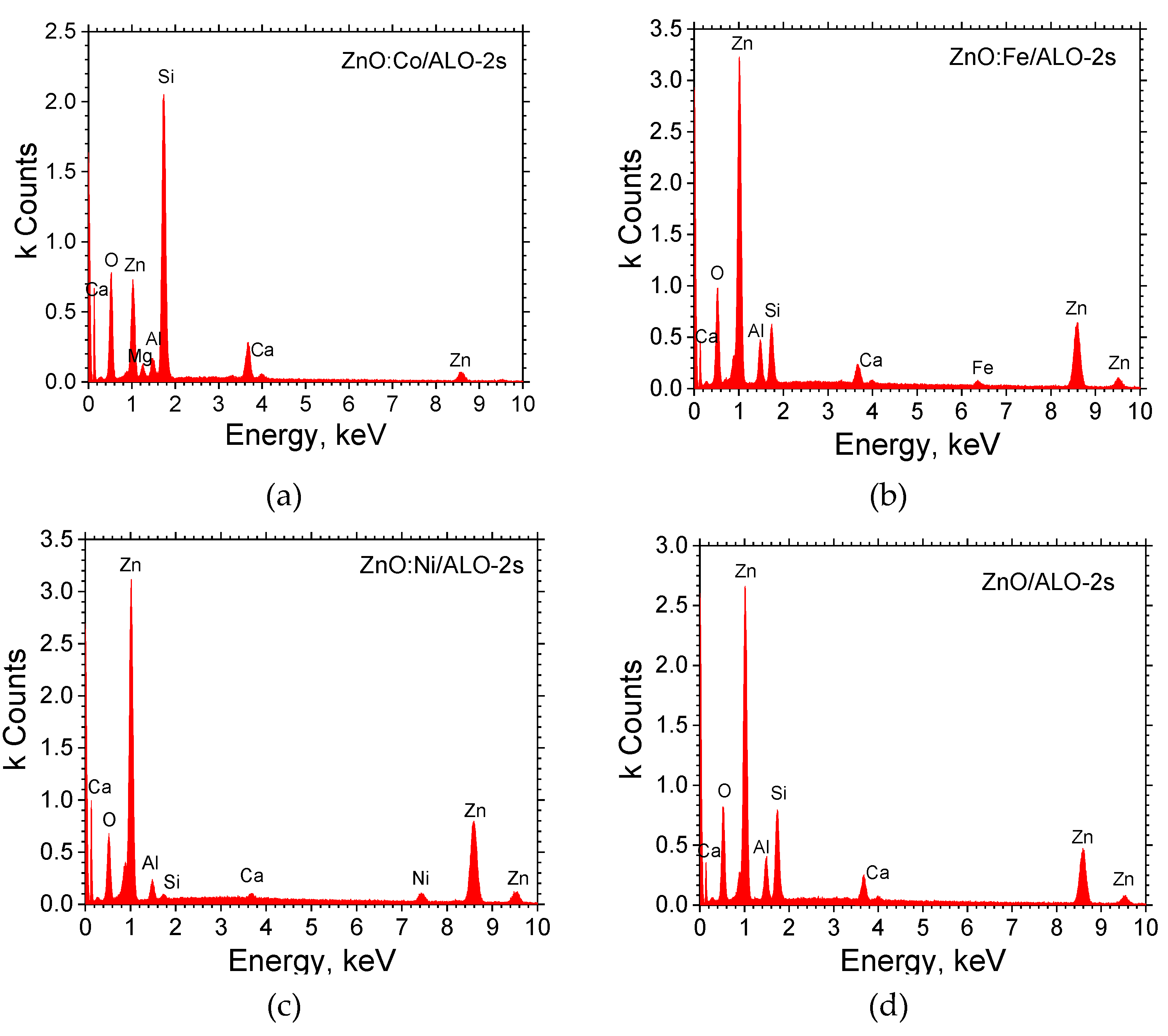
Figure 5.
XRD of ZnO:TM/ALO fibers.
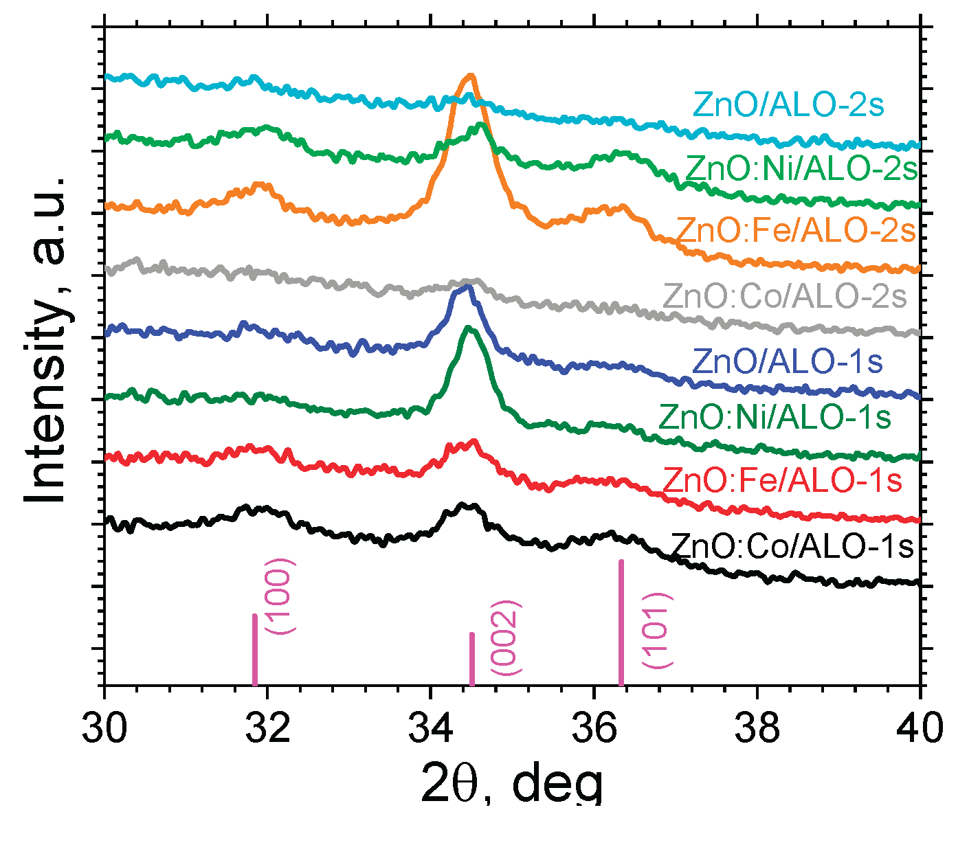
Figure 6.
XPS of ZnO:TM/ALO fibers.
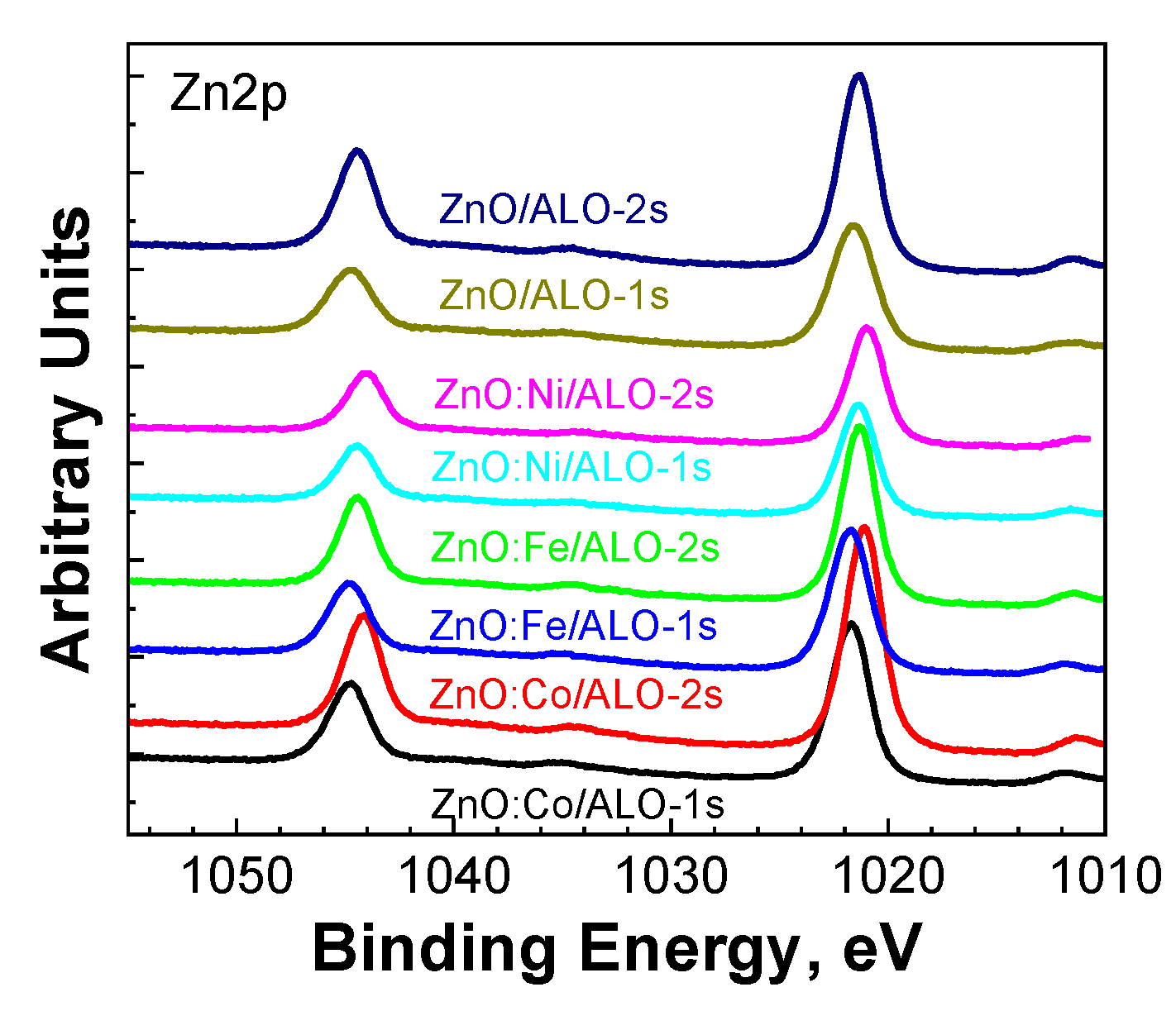
Figure 7.
XPS of O1s of ZnO:TM/ALO fibers.
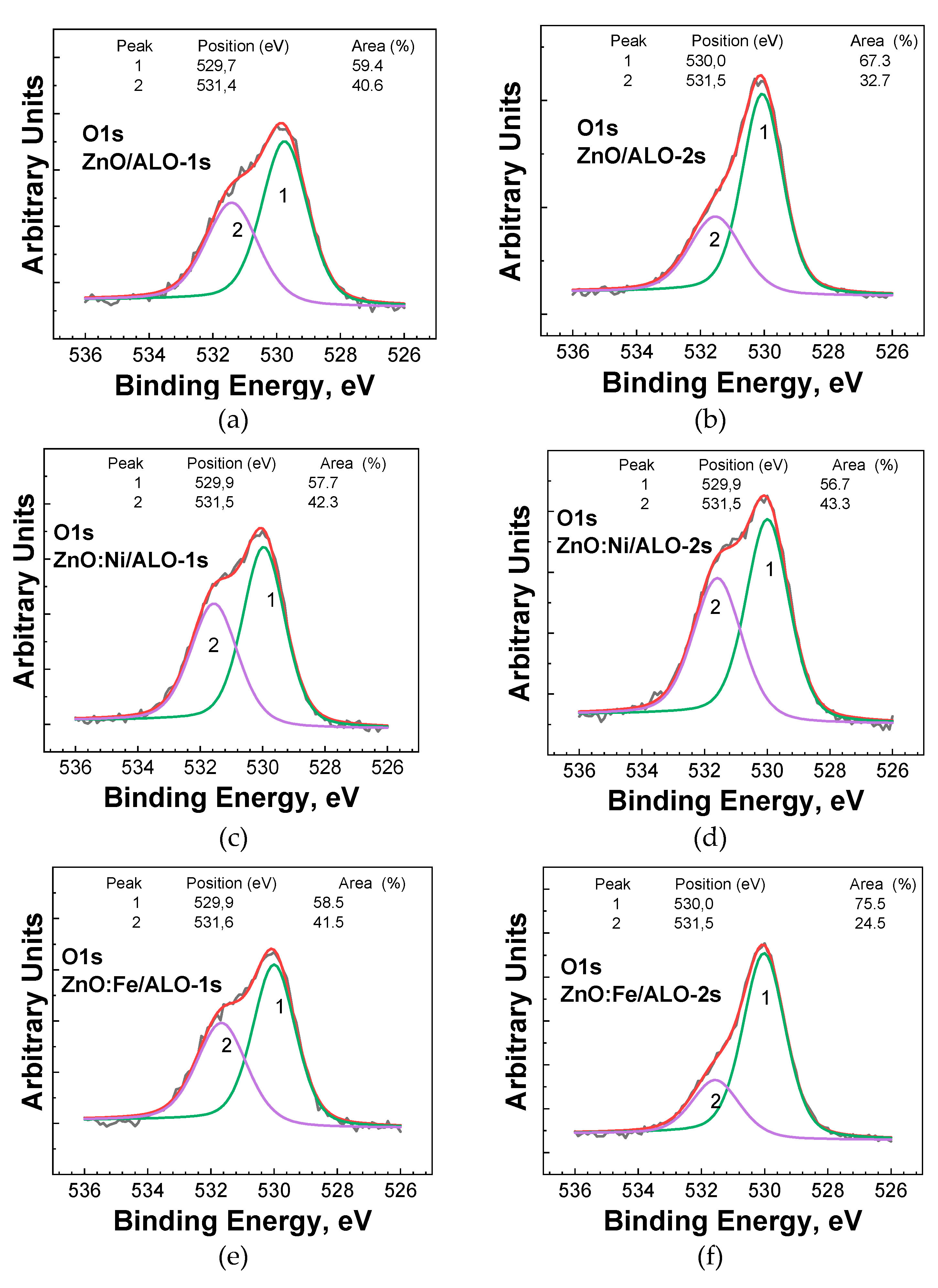
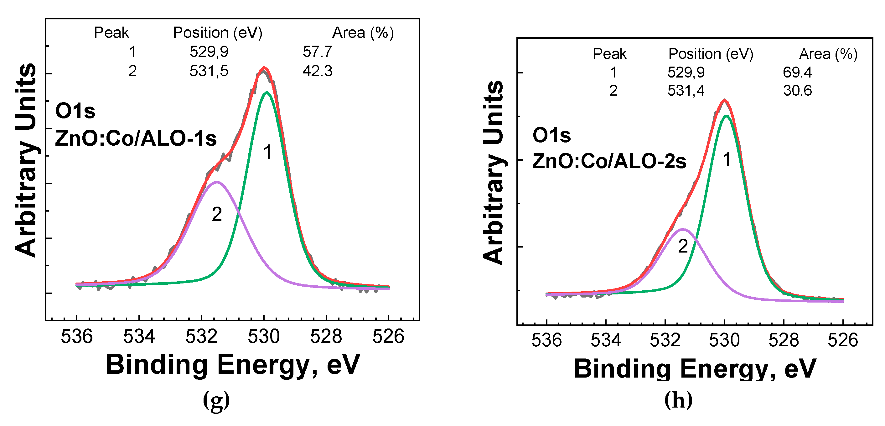

Table 1.
ALD parameters.
| Series | Number of Cycles | Temperatures, ℃ | Hollow Fiber Structures | |||
| ZnO | TMO 1 | supercycle | Reactor | HS 2 | ||
| 1 | 16 150 |
50 | 80 | 200 | 800 | ZnO:TM/ALO-1s ZnO/ALO-1s |
| 2 | 6 150 |
200 | 250 | 230 | 900 | ZnO:TM/ALO-2s ZnO/ALO-2s |
1 TMO – Co, Fe, Ni oxides; 2 HS – Hot Source temperature; ALO – Al2O3.
Table 2.
Hollow fiber parameters of Series 1 (1s) and Series 2 (2s) obtained by SEM and ellipsometry.
Table 2.
Hollow fiber parameters of Series 1 (1s) and Series 2 (2s) obtained by SEM and ellipsometry.
| Fiber Structure | dia, nm | wall, nm |
| PVA | 338 | - |
| ZnO:Co/ALO-1s | 312 | 59 |
| ZnO:Fe/ALO-1s | 338 | 58 |
| ZnO:Ni/ALO-1s | 420 | 72 |
| ZnO/ALO-1s | 382 | 73 |
| ZnO:Co/ALO-2s | 319 | 96 |
| ZnO:Fe/ALO-2s | 306 | 89 |
| ZnO:Ni/ALO-2s | 375 | 137 |
| ZnO/ALO-2s | 316 | 81 |
Table 3.
Crystallite sizes of ZnO.
| Fiber Structure | D, nm |
| ZnO:Co/ALO-1s | 7.5(3) |
| ZnO:Fe/ALO-1s | 7.3(3) |
| ZnO:Ni/ALO-1s | 14.6(6) |
| ZnO/ALO-1s | 12.7(5) |
| ZnO:Co/ALO-2s | 9.7(8) |
| ZnO:Fe/ALO-2s | 11.8(2) |
| ZnO:Ni/ALO-2s | 8.3(3) |
| ZnO/ALO-2s | 7.1(5) |
Disclaimer/Publisher’s Note: The statements, opinions and data contained in all publications are solely those of the individual author(s) and contributor(s) and not of MDPI and/or the editor(s). MDPI and/or the editor(s) disclaim responsibility for any injury to people or property resulting from any ideas, methods, instructions or products referred to in the content. |
© 2025 by the authors. Licensee MDPI, Basel, Switzerland. This article is an open access article distributed under the terms and conditions of the Creative Commons Attribution (CC BY) license (http://creativecommons.org/licenses/by/4.0/).
Copyright: This open access article is published under a Creative Commons CC BY 4.0 license, which permit the free download, distribution, and reuse, provided that the author and preprint are cited in any reuse.


