
Submitted:
08 July 2025
Posted:
09 July 2025
You are already at the latest version
Abstract
This research paper addresses the problem of testing n×1 random-access memories (RAMs) in which complex models of unlinked static neighborhood pattern-sensitive faults (NPSF) are considered. Specifically, two well-known fault models are addressed: the classical NPSF model that includes only memory faults sensitized by transition write operations and an extended NPSF model that covers faults sensitized by transition write operations as well as faults sensitized by non-transition writes or read operations. For these NPSF fault models, near-optimal multirun march memory tests suitable for implementation in embedded self-test logic are proposed. The assessment of the optimality is based on the fact that, for any group of cells corresponding to the NPSF model, the state graph is completely covered and each arc is traversed only once, which means that the graph is of the Eulerian type. Additional write operations are only required for data background changes. A characteristic of a memory test algorithm where multiple data backgrounds are applied is that test data is always correlated with the address of the accessed location. For easy implementation in embedded self-test logic, the proposed tests use 4×4 memory initialization patterns rather than the more difficult-to-implement 3×3 patterns, as is the case with other currently known near-optimal memory tests.
Keywords:
RAM testing
; static unlinked neighborhood pattern-sensitive faults
; near-optimal tests
; Eulerian graph
; built-in self-testing
1. Introduction
As shown in the International Roadmap for Devices and Systems (IRDS) edited by the IEEE Computer Society or in works such as [1,2,3], in System on Chip (SoC) or Network on Chip (NoC), the memory part has a growing share, currently covering 75-85% of the integrated area. Therefore, in the production of reliable integrated circuits at competitive costs, efficient testing of the memory part is a very important requirement.
In this paper, the authors address the issue of testing RAMs with regard to the complex fault model of static unlinked neighborhood NPSFs, as a subclass of coupling faults (CFs) model [4,5]. According to the classification of memory faults, as presented for example in [2,6,7,8], the ‘static faults’ class refers to those faults sensitized by performing at most one memory operation, while the ‘dynamic faults’ class refers to those faults sensitized by two or more operations performed sequentially. According to the same taxonomy presented in [6] or [7], for example, CFs are said to be unlinked when they do not influence each other. In this paper, the class of static unlinked CFs is addressed.
The CF model reflects imperfections in the memory cell area that cause two or more cells to influence each other in their operation [2,3]. Depending on the number of cells involved in a memory fault, there are several classes of coupling faults, such as: two-cell coupling, three-cell coupling, four-cell coupling, or five-cell coupling. In the two-cell CF model, it is considered that the cells involved in a CF can be anywhere in the memory [9]. In this way, this model also covers addressing memory faults [6]. For more complex -cell CF models, , it is assumed that the cells involved in a memory fault are physically adjacent [5,10,11]. It is therefore necessary to know the memory structure, or more precisely the correspondence between logical addresses and physical addresses, in the form of row and column addresses. This realistic limitation allows the complexity of these fault models to be more easily managed [12,13,14]. For these complex CF models, testing is usually done with additional integrated architectures, called built-in self-test (BIST) logic [15,16,17,18,19,20].
Regarding the -cell CFs, depending on the technology used, the accuracy of the testing, and the costs involved, two classes of fault models have been defined to cover the most common memory errors, namely: (a) the classical model class in which it is considered that a memory fault can be sensitized only by a transition write operation, and (b) an extended class of models in which it is admitted that memory faults can be sensitized by transition write operations, as well as by non-transition writes or read operations – extended CF models (ECF) [9,12,13,14]. With the increase in density and the decrease in supply voltage, the range of memory defects has diversified, and as a result, for high testing accuracy, ECF models are increasingly used. The authors appreciate, however, that a memory test covering the classical CF model can be adapted relatively easily to cover the corresponding ECF model [12]. This is also highlighted in this work.
For three-cell or four-cell classical CF models, reference tests are reported in [10,11,21,22,23,24]. For three-cell or four-cell ECF models, near-optimal tests are presented in [14].
In this paper, we focus exclusively on the NPSF fault model involving five physically adjacent memory cells, arranged in a configuration like the one shown in Figure 1.
This NPSF fault model, which reflects the influence of neighboring cells on the central memory cell, has been defined since the 1970s [25]. Specifically, we refer here to the classical NPSF model in which a fault sensitization involves a transition write operation in one cell in the group, the other four cells being in a certain state that favors the occurrence of the memory error. The scientific community has continuously studied the NPSF model because of its importance and complexity. Memory testing for NPSF models is covered extensively in books, like [2,3,4,26], and in review papers, such as [16,17,19].
For the NPSF model, some memory tests have been proposed since the 1980s, that were quite effective for the memory sizes of that period [27,28]. For example, the memory test given by Suk and Reddy [28] is based on an algorithm for dividing the set of memory cells into two halves, based on row and column addresses, and is long. A reduction in testing time was possible by applying march-type tests on different memory initialization patterns (data backgrounds). This idea was first proposed by Cockborn [23]. This technique, called ‘multirun march memory testing’, was then used to identify efficient memory tests for this complex NPSF model [29,30,31,32]. For example, in [31], to reduce the length of the test, Buslowska and Yarmolik propose a multirun technique with a random background variation. However, in that case, the NPSF model is not fully covered. A first near-optimal deterministic memory test for the NPSF model was proposed by Cheng, Tsai, and Wu in 2002 [32]. This memory test called is long and uses 16 memory initialization patterns of size 3×3. Ten years later, Huzum and Cascaval [33] improved this result with another near-optimal memory test (called ), slightly shorter, of length Compared to the , the memory test applies a different testing technique, but also uses 3×3 data background patterns. The and tests are the shortest memory tests dedicated to this complex NPSF model. Although near-optimal, these tests are not exactly suitable for BIST implementation due to the complexity of the address-based data generation logic. More on this issue can be found in the works [34,35,36,37,38,39,40], but an in-depth analysis is also presented in this paper. For this reason, Cheng, Tsai and Wu also proposed in the same article [32] another memory test () which, although longer (and obviously non-optimal), is easier to implement in BIST-RAM architectures due to its 4×4 memory initialization patterns. A modified version of the memory test for diagnosis of SRAM is given by Julie, Sidek, and Wan Zuha [36].
In this work, a new near-optimal test () able to cover the classical NPSF model is proposed. This new test is of length and uses 16 data backgrounds with patterns of 4×4 in size, making it suitable for implementation in BIST-RAM architectures. Compared to the test, this new memory test is significantly shorter and has a simpler structure. The synthesis of the address-based data generation logic for this memory test, considering a possible BIST implementation, is also discussed. This work also highlights the simplicity of address-based data generation logic in the case of 4×4 data backgrounds, compared to 3×3 ones. For the extended NPSF model (ENPSF), a near-optimal test of length is proposed.
The remainder of this paper is organized as follows. Section 2 presents assumptions, notations, and some preliminary considerations related to multirun memory tests, or to the necessary and sufficient conditions for detecting memory coupling faults. Section 3 describes new near-optimal memory tests for the classical NPSF model and the extended NPSF one, respectively, that use 4×4 data background patterns. Section 4 presents a synthesis of data generation logic for memory operations, for a possible BIST implementation of the proposed memory tests. To emphasize the advantage of the proposed tests, compared to other known memory tests that use 3×3 background patterns, where modulo 3 residues are required for row and column addresses, an additional analysis showing the complexity of generating modulo 3 residues is presented in the Appendix. Section 5 completes the paper with some conclusions regarding this work.
2. Assumptions, Notations and Preliminaries
2.1. Assumptions
As in other works dedicated to NPSF models, it is assumed that the memory structure is fully known, so that based on the physical address information a multirun march test can be applied using different data backgrounds. Of course, in the memory, there can be one or more groups of coupled cells. As in other similar works, such as [4,26,30,31,32,33,34,35], it is assumed that the coupled cell groups are disjoint.
2.2. Notations
The notations used to describe memory operations or certain memory errors are shown below.
| Operation of reading a memory cell and checking the value read by comparing it with the expected one. | |
| Operation of writing the logical value 0 (1) to the addressed cell. | |
| Write operation to change the state of the addressed cell (transition write operation). | |
| Write operation without changing the state of the addressed cell (non-transition write operation). | |
| , | Memory operations with cell . |
| () | A change of logical state in a memory cell from to 1 (to 0) by sensitizing a memory fault (i.e., a memory error). |
| Row (column) address in a memory operation. | |
| The logical value of memory cell . |
2.3. Preliminaries
A march memory test consists of a set of march items, each of them describing a sequence of operations that must be performed successively on all memory locations (moving to the next cell is done only after performing all operations on the current one). The first symbol of a march element specifies the order in which memory locations are accessed. Given a sequential enumeration of memory addresses, the symbol ⇑ indicates that these addresses are traversed in ascending order, while the symbol ⇓ indicates that they are traversed in reverse order.
In the case of multirun testing, a given march test is applied repeatedly on different data backgrounds. A data background is obtained by multiplying a data pattern in memory, both horizontally and vertically. Such a testing technique is currently used for any multi-cell CF model. Data backgrounds with row stripe, column stripe, or checkerboard patterns are commonly used in multirun-type memory testing [12,13]. For these data backgrounds the initialization patterns are of size 2×2. But the NPSF model we consider requires more complicated initialization patterns, concretely of size 3×3 or 4×4, as shown in [32,33], and as presented extensively in this work. Specifically, a data background pattern must completely cover the five-cell configuration shown in Figure 1 and, for this reason, the pattern must be at least 3×3 in size.
Generally, for a -cell CF model, the affected cell (the cell where the memory error occurs) is considered () and the other cells in the group are considered to be () [7]. In order to describe more clearly how a memory fault is sensitized, sometimes the cell where the fault sensitizing operation is performed is considered to be the , and the other cells in the group which, by the state they are in, allow the appearance of the memory error, are called () [6,7]. These aspects are illustrated in Figs 2 and 3. Since neighboring cells can exert a passive or active influence on the central cell, the NPSF model includes two types of faults, passive NPSF and active NPSF, as shown in Figure 2 and Figure 3, respectively [27,28].
Specifically, in the case of passive NPSF, a configuration of neighboring bits prevents a certain transition in the central cell, from 0 to 1 or from 1 to 0, as appropriate. In the case of an active NPSF, making a transition in one of the neighboring cells (aggressor cell), in a certain state of the other cells that facilitate the occurrence of the error (enabling cells), can cause the state to change in the central cell as well (↑ or ↓, as appropriate). The classical NPSF model comprises passive fault primitives and active fault primitives [41].
To detect a memory error, the test must sensitize the fault with a suitable transition write operation and then read the victim cell to observe the error. For the classical NPSF model, in terms of satisfying the sensitization condition of any fault, a memory test must entirely cover the state transition graph for any group of five cells in the known configuration.
Let be a group of five cells as shown in Figure 1, where , which means that when memory addresses are traversed in ascending order (⇑), the cells are accessed in this order, and when memory addresses are traversed in descending order (⇓), the cells are accessed in the reverse order. Given this aspect, it can be said that a memory test is optimal if, for any group of cells, any transition write operation in the state graph is performed once and only once (i.e., for any group of cells, the state graph is Eulerian).
Considering the two types of NPSF faults (passive and active faults), as also mentioned in other works, e.g. [2,4,9,10], in order to detect any error resulting from memory fault sensitization, two necessary and sufficient observability conditions must be met:
) A memory cell must be read after performing a fault sensitizing operation, prior to a new write, to verify that this operation was performed correctly.
) Before writing to a cell, it must first be read, to verify that a state change has not occurred as a result of an operation previously performed in another possibly aggressor cell.
3. Near-Optimal March Tests for the NPSF Model
To cover the classical NPSF model, where a fault sensitization involves a transition write operation in a cell of the coupled cell group with the configuration shown in Figure 1, a new memory test is proposed, called . In this test, two march elements are applied sixteen times on different data backgrounds (i.e., a multirun technique). The description of this new march multirun memory test is given in Figure 4, and the sixteen patterns used for memory initialization are shown in Figure 5.
In this description, indicates the primary memory initialization sequence while , , represent test sequences with background changes, according to the patterns shown in Figure 5. Note that, any change of data background involves a status update only for half of the memory cells. On the other hand, in order to satisfy the observability condition, any write operation to change the state of a memory cell is preceded by a read operation. Thus, the initialization sequence , which is of the form , involves write operations, while a test sequence with background change, , , requires read operations and write operations. Thus, the length of the memory test is:
The ability of the memory test to cover the NPSF model is discussed in the following.
Theorem 1
. The test algorithm is able to detect all unlinked static faults of this classical NPSF model.
The ability of the test algorithm to sensitize and observe any fault that may affect a cell in a cell group is demonstrated in the following.
To prove this statement, it is shown that during the memory testing, performs all possible operations in the group of cells . In other words, completely covers the graph of states describing the normal functioning of cells in this group.
Given that the test uses 4×4 memory initialization patterns, it follows that the cells selected 4 by 4 per row or column are brought to the same initial state and, consequently, the same operations are then performed on them during the application of a march element. Starting from this observation, the memory cells are divided into 16 classes (subsets), depending on the residues of the row address modulo 4 () and the column address modulo 4 (), as shown in the following table (Table 1).
This division of the memory cell set into 16 classes according to row and column addresses is illustrated in Figure 6.
Let now be the subset of all -groups of five cells in the known configuration for which the base cell . This class division of the -groups of five cells is also illustrated in Figure 6. This figure shows that the cells in the neighborhood of the base cells also belong to the same classes. For example, for the groups of cells in the subset , the cells identified with belong to , those identified with belong to , and so on.
In the following, let us analyze the initial state for a group of five memory cells in the known configuration, depending on the data background and the class of groups it belongs to .
The status code for a group of cells is a word that includes the five logical values of the component cells, in the form . It is worth noting that a group of cells in the state will reach the complementary state when the march element is applied. We say that and are complementary states because for any pair and the following relation holds:
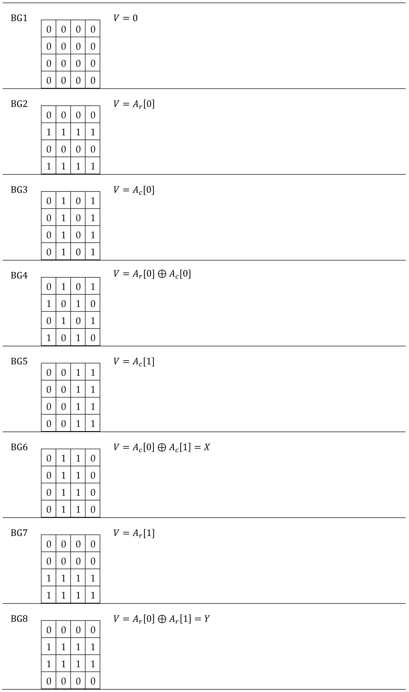
Figure 7 illustrates the initial and complementary states, and , for two groups of cells depending on data background, BG, namely andThe initial state and the complementary one for a group of cells in the known configuration, depending on the initialization pattern and the class of which the group belongs , are presented in Table 2. In this table, it can be verified that for any group of five neighboring cells in the known configuration, regardless of the class to which the group belongs (i.e., any column), the 16 background changes result in 16 distinct initial states, such that
Furthermore, for any column in Table 2, the following equation is valid:
If represents the set of all states (as in the truth table), based on (3) and (4) we can write:
Note that the states in any of the 16 columns of Table 2 satisfy equation (5), which means that all initial states and their complementary ones are different from each other and all together form the set .
As a remark, identifying those initialization models for which this property is fulfilled has involved a considerable research effort.
It is also important to note that, starting from an initial state , upon execution of the first march element (of the form ), a group of cells is brought to the complementary state , and after the next march element (identical to the first), that group of cells is returned to the initial state .
Based on all these aspects, we can conclude that any group of cells in the known configuration is brought into each of the 32 possible states, and then a march element of the form is applied.
In a full memory scan with the march element , 5 different transitions are performed in any group of five cells. On the whole, in a group of five cells, transitions are performed. For example, Figure 8 shows the transitions performed in a group of cells of class in the first 6 of the 16 stages of the memory test. The initial states after the 6 background changes are highlighted in bold. For easier identification, the transitions performed at each iteration are shown in different colors, and for the first transition within an iteration, an identification number is written on the edge.
Next, it is shown that all 160 transitions performed in a group of cells are different transitions and therefore the state transition graph is completely covered.
Figure 9 shows the evolution of the states for a group of cells , starting from two different initial states, , when the march element is applied. The intermediate states that appear in the figure, and , are detailed in Table 3.
From Table 3, it follows that, since , Note that although often, in the two cases, the write operations are performed on different memory cells and therefore the respective transitions are also different. Several such cases are found in Figure 8, such as the transitions made in the states 10000, 10100, 10010 or 01001.
In conclusion, by applying the memory test, different transitions are performed in the -group of cells, completely covering the state transition graph. Moreover, each of these transitions is performed only once. As a result, the sensitization condition for all coupling faults specific to this classical NPSF model is met.
Proving this property involves verifying the fulfillment of the two observability conditions, and , presented in Section 2. For an easier and more direct verification of the fulfillment of the observability conditions, Figure 10 shows all the operations performed in a group of cells during the execution of the memory test. In the sequence of operations performed on cells in group , write operations for initialization or background change are written in normal font, and those with the role of memory fault sensitization are highlighted in blue. Read operations that have the role of detecting possible errors resulting from fault sensitization are written in red.
Analyzing the sequence of operations shown in Figure 10, it can be seen that when a cell is accessed, it is first read, thus checking whether a state change has occurred in the cell, as a result of an influence from another aggressor cell. This check is required by condition . Also, by analyzing the sequence of operations illustrated in this figure, it can be seen that after performing a write operation on a cell, it is then read (immediately or later) to verify that the operation was performed correctly. Thus, condition is also met.
With the verification of both conditions regarding the sensitization of all considered memory faults and the ability to detect any resulting errors, the proof of the theorem is complete. ?
Remark 1.
For any group of cells that corresponds to the considered NPSF model, the state transition graph is completely covered, and furthermore, each transition is performed only once. That means that the graph of states is Eulerian. The only redundant operations are used for background changes. With this argument, it can be said that this memory test is near-optimal.
The proposed memory test can be adapted to cover the extended NPSF model (ENPSF), in which memory faults can be sensitized by transition write operations but also by read or non-transition write operations [41]. To this end, the two march elements of form are extended to the form . This extension leads to a near-optimal memory test for the ENPSF model, called , of length , as shown in Figure 11.
Note that in this case, when a certain state is reached, the and operations are first executed and checked, and then the state is changed by a operation.
Remark 2.
The ability of each of the two memory tests to cover the considered NPSF model was also verified by simulation. In the case of faults sensitized by transition write operations, the TRAP interrupt was used to simulate memory errors. For the other memory faults, dedicated simulation programs were required.
4. Considerations for BIST Implementation of the Proposed Memory Tests
In this section, a possible synthesis of the data generation logic for memory operations is discussed, considering a possible BIST implementation of the proposed memory test. Specific to such a multirun test is the dependency between the value of a memory cell and its address. It should be noted that 4×4 background patterns allow for a simple synthesis of data generation logic. This is due to the fact that the logical value for the current cell is generated based on the two least significant bits (LSB) of the row address, and , and/or the column address, and . Table 4 presents a possibility of generating data based on the address depending on data background. The memory initialization patterns are taken into the table for easier verification.
The MT_NPSF_81N memory test repeats two march elements 16 times, on different background patterns. Consequently, in order to adapt the logical value of the accessed cell to the background, a test sequence counter of length 4 and a 16-input multiplexer are required. Considering the relationships between date and address depending on the data background, as presented in Table 4, a possible solution for the data generation logic is shown in Figure 12.
The command that appears in the data generation logic, provided by the control logic, is required to perform transition write operations in the first memory scan and read operations in the second, as highlighted in blue in this test sequence: .
This synthesis shows that the memory test, despite using a large number of initialization patterns with some irregular structures, can be implemented quite easily in BIST-RAM architectures.
For comparison, let us analyze the possibility of implementing in self-testable structures the other two near-optimal memory tests dedicated to this classical NPSF model reported so far, [33] and [34], which are somewhat shorter but use memory initialization patterns of size 3×3. In a memory test using 3×3 background patterns, the address-based data generation requires generating the modulo 3 residues of the row and column addresses. But this is a very complicated issue. The difficulty of hardware generation of modulo 3 residues is highlighted in the Appendix. This is the major disadvantage of memory tests that use 3×3 data background patterns. For this reason, the authors argue that the new memory test, although slightly longer, is more suitable for implementation in self-testing RAM structures, compared to the other two known near-optimal memory tests, and .
5. Conclusion
The paper proposes two near-optimal memory tests dedicated to the complex NPSF model, both in the classic version in which it is accepted that a fault is only sensitized by a transition write operation, and in the extended version in which faults sensitized by a non-transition write or a read operation are also taken into account. The proposed tests, and , respectively, are multirun march memory tests that use 4×4 data background patterns and are specifically designed to be easy to implement in self-testing RAM architectures. These are the first near-optimal memory tests dedicated to the NPSF model using 4×4 data initialization patterns reported to date.
Due to the difficulty of generating modulo 3 residues for row and column addresses (an aspect highlighted in detail in the appendix), the authors state that memory tests using 3×3 memory initialization patterns (as are the other two known near-optimal tests for the classical NPSF model, and ) are not exactly suitable for implementation in self-testing RAM structures.
The evaluation of the optimality of the proposed tests is based on the fact that, for any group of cells corresponding to the NPSF model, the state graph is completely covered, and each arc is traversed only once, which means that the graph is Eulerian. Some additional memory write operations are only required for background changes. All these aspects were also verified through simulation.
The memory initialization patterns were designed so that any group of five cells in the known configuration would be brought into each of the 32 possible states, only once. A great deal of research effort was required to fulfill this condition. The authors identified this optimal solution intuitively, but in future research they will try to identify other solutions through search methods specific to artificial intelligence.
Supplementary Materials
The following supporting information can be downloaded at the website of this paper posted on Preprints.org.
Funding
This research received no external funding.
Acknowledgements
The authors thank their colleague Prof. Florin Leon for useful and fruitful discussions. Also, special thanks to Dr. Viorel Onofrei for the useful suggestions that contributed to improving the readability of this paper
Conflicts of Interest
The authors declare no conflict of interest.
Appendix A. Hardware Generation of Modulo 3 Residues
For a nonnegative integer , let be the remainder (residue) of dividing by . As is of the form
then can be calculated starting from the well-known equation [42, pages 37-59]:
But, for numbers that represent powers of , the values of are shown in Table A1.

Table A1.
Values for
| 0 | 1 | 2 | 3 | 4 | 5 | 6 | ||
| 1 | 2 | 4 | 8 | 16 | 32 | 64 | ||
| 1 | 2 | 1 | 2 | 1 | 2 | 1 |
Based on (A2) and the values in Table A1, the following equation results:
Equation (A3) highlights the fact that the values of the coefficients on even positions and, respectively, those of the coefficients on odd positions have equal weights in calculating the value. Therefore, the evaluation of (A2) starts from calculating the residue modulo 3 for the sum of two consecutive terms, one in even position and the other in the immediate next odd position .
Let us consider the value expressed in redundant form as follows:
For the sum of two consecutive terms , the logical valuesare determined based on the following truth table:
From the truth table, for the output variables the following equations result:
Let us denote by CLC1 the network of logic gates that performs these operations. The structure of this combinational logic circuit is given in Figure A1.
For two pairs of coefficients of this type, identified as and , the outputs are denoted by and, respectively. These intermediate results are then processed by another combinational logic circuit, called CLC2, which generates the remainder of the sum divided by 3 in the form , as shown in the Figure A2.
The logical values are obtained based on the following equations:
The network of logic gates that performs these operations is given in Figure A3.
For a word =, calculating the value of requires CLC1 structures on the first level and a number of other CLC2 structures on the following levels. This results in a series-parallel logical structure. Operations on the same level are performed in parallel, and those on different levels are performed in series. Such a series-parallel structure for is shown in Figure A4.
Figure A4 highlights the complexity of the logical structure for determining modulo 3 residues. In addition, if is not a power of 2, the calculation logic is even more complicated, and in a memory, for row or column addresses, this condition is usually not met.
References
- Chakravarthi, V. S., A practical Approach to VLSI System on Chip (SoC) Design: A Comprehensive Guide, Second Edition, Springer, 2022.
- Dean Adams, R., High Performance Memory Testing: Design Principles, Fault Modeling and Self-Test, Springer, New York, NY, USA, 2003.
- Mazumder, P., Chakraborty, K., Testing and Testable Design of High-Density Random-Access Memories (Frontiers in Electronic Testing), Kluwer Academic, Boston, Mass, USA, 1996.
- Mrozek, I., Multi-run Memory Tests for Pattern-Sensitive Faults, Springer, 2019.
- Ramana Kumari, K. L. V., Asha Rani, M., Balaji, N., 3-Cell Neighborhood Pattern-Sensitive Fault Testing in Memories Using Hamiltonian and Gray Sequences, Journal of Computational and Theoretical Nanoscience, Vol. 18 (3), pp. 879-884, March 2021.
- Hamdioui S., Testing Static Random-Access Memories: Defects, Fault Models and Test Patterns, Kluwer Academic Publishers, The Netherlands, 2004.
- van de Goor, A.J., Al-Ars, Z., Functional Faults Models: A Formal Notation and a Taxonomy, Proc. 18th IEEE VLSI Test Symp., Montreal, Canada, April-May 2000, pp. 281-289.
- Samanta, A., Saha, M., Mahato, A.K., BIST Design for Static Neighbourhood Pattern-Sensitive Fault Test, IJCA Proc. on International Conference on Communication, Circuits and Systems 2012 iC3S (5): 23-28, June 2013.
- Harutunyan, G., Vardanian, V.A., Zorian, Y., Minimal March Tests for Unlinked Static Faults in Random Access Memories, Proc. of 23rd IEEE VLSI Symposium, Palm Springs, CA, USA, May 2005, pp. 53–59.
- Cascaval, P., Bennett, S., Efficient March Test for 3-Coupling Faults in Random Access Memories, Microprocessors and Microsystems, Elsevier, Vol. 24 (10), 2001, 501-509.
- Cascaval, P., Bennett, S., Hutanu, C., Efficient March Tests for a Reduced 3-Coupling and 4-Coupling Faults in RAMs, Journal of Electronic Testing. Theory and Applications, Vol. 20 (2), 2004, pp. 227-243.
- Cascaval, P., Cascaval, D., March SR3C: A Test for a Reduced Model of All Static Simple Three-Cell Coupling Faults in Random-Access Memories, Microelectronics Journal, Vol. 41 (4), 2010, pp. 212-218.
- Cascaval, P., Cascaval, D., March Test Algorithm for Unlinked Static Reduced Three-Cell Coupling Faults in Random-Access Memories, Microelectronics Journal, Vol. 93, November, 2019.
- Cascaval, P., Cascaval, D., Near-optimal March Tests for Three-Cell and Four-Cell Coupling Fault Models in Random-Access Memories, Romanian Journal of Information Science and Technology, Vol. 27 (3-4), 2024, 323–335.
- Mrozek, I; Shevchenko, NA and Yarmolik, VN, Universal Address Sequence Generator for Memory Built-in Self-Test, Fundamenta Informaticae, Vol. 188 (1), 41-61, Dec. 2022. [CrossRef]
- Jidin, A.Z., Hussin, R., Fook, L.W., Mispan, M.S., A Review Paper on Memory Fault Models and Test Algorithms, Bulletin of Electrical Engineering and Informatics, Vol. 10 (6), 2021, 3083-3093.
- Hantos, G., Flynn, D., Desmulliez, M.P.Y., Built-In Self-Test (BIST) Methods for MEMS: A Review. Micromachines, Vol. 12 (1), 40, 2020.
- Zhang, L.; Wang, Z.; Li, Y.; Mao, L., A Precise Design for Testing High-Speed Embedded Memory Using a BIST Circuit, IETE Journal of Research, Vol. 63, pp. 473–481, 2017.
- Thakur, R.S., Awasthi, A., A Review Paper on Memory Testing Using BIST, Global Research and Development Journal for Engineering, Vol. 1 (4), 2016, pp. 94-98.
- Hou, C., Li, J., Fu, T., A BIST Scheme with the Ability of Diagnostic Data Compression for RAMs, IEEE Transactions on Computer-Aided Design of Integrated Circuits and Systems, Vol. 33 (12), 2014, pp. 2020-2024.
- Nair, C., Thatte, S.M., Abraham, J.A., Efficient Algorithms for Testing Semiconductor Random-Access Memories, IEEE Transactions on Computers, C-27 (6), 1978, pp. 572–576.
- Papachristou, C.A., Saghal, N.B., An Improved Method for Detecting Functional Faults in Random-Access Memories, IEEE Transactions on Computers, C-34 (2), 1985, pp.110–116.
- Cockburn, B.F., Deterministic Tests for Detecting Single V-Coupling Faults in RAMs, Journal of Electronic Testing: Theory and Applications, Vol. 5, pp. 91–113, 1994.
- Wu, T.C., Fan, W.K., et al, A New Test Algorithm and Fault Simulator of Simplified Three-Cell Coupling Faults for Random Access Memories, IEEE ACCESS, Vol. 12, 2024, 109218-109229.
- Hayes, J.P., Detection of Pattern-Sensitive Faults in Random-Access Memories, IEEE Transactions on Computers, Vol. C-24 (2), 1975, pp. 150 – 157.
- Ramana Kumari, K.L.V., Asha Rani, M., Balaji, N., Testing of Neighborhood Pattern-Sensitive Faults for Memory. In: Reddy, V.S., Prasad, V.K., Wang, J., Reddy, K.T.V. (eds) Soft Computing and Signal Processing. Advances in Intelligent Systems and Computing, Vol. 1340, Springer, Singapore, 2022.
- Hayes, J. P., Testing Memories for Single-Cell Pattern-Sensitive Faults, IEEE Transactions on Computers, 29 (3), 1980, pp. 249–254.
- Suk, D., Reddy, S., Test Procedures for a Class of Pattern-Sensitive Faults in Semiconductor Random-Access Memories, IEEE Transactions on Computers, C-29 (6), 1980, pp. 419-429.
- Karpovsky, M.G., Yarmolik, V.N., Transparent Random-Acces Memory Testing for Pattern-Sensitive Faults, Journal of Electronic Testing. Theory and Applications, Vol. 9, Dec. 1996, pp. 860-969.
- Kang, D. C., Cho, S. B., An Efficient Build–in Self–Test Algorithm for Neighborhood Pattern-Sensitive Faults in High–Density Memories, Proc. 4th Korea–Russia Int. Symp. Science and Technology, 2000, Vol. 2, pp. 218–223.
- Buslowska, E., Yarmolik, V. N., Multi-Run March Tests for Pattern-Sensitive Faults in RAM, 2018 IEEE East-West Design & Test Symposium (EWDTS 2018), SEP 14-17, 2018, Kazan, Russia.
- Cheng, K.L., Tsai, M.F., Wu, C.W., Neighborhood Pattern-Sensitive Fault Testing and Diagnostics for Random-Access Memories, IEEE Transactions on Computer-Aided Design of Integrated Circuits and Systems, Vol. 21 (11), 2002, 1328-1336.
- Huzum, C., Cascaval, P., A Multibackground March Test for Static Neighborhood Pattern-Sensitive Faults in Random-Access Memories, Electronics and Electrical Engineering (Elektronika ir Elektrotechnika) – Section System Engineering, Computer Technology, Vol. 119 (3), 81-86, April 2012.
- Wang, L.T., Wu, C.W., Wen, X., Memory Testing and Built-In Self-Test. In VLSI Test Principles and Architectures, 1st ed.; Design for Testability, Elsevier, Amsterdam, The Netherlands, 2006.
- Bernardi, P., Grosso, M., Sonza Reorda, M., Zhang, Y., A Programmable BIST for DRAM testing and diagnosis, IEEE International Test Conference, 2-4 Nov, 2010, Austin, TX, USA, pp: 1-10.
- Rusli, J. R.; Sidek, R. M.; Wan Zuha, W. H., Development of Automated Neighborhood Pattern Sensitive Fault Syndrome Generator for SRAM, 10th IEEE Int. Conf. on Semiconductor Electronics (ICSE), Kuala Lumpur, Malaysia, Sept 19-21, 2012.
- Cascaval, P., Silion, R., Cascaval, D., A Logic Design for MarchS3C Memory Test BIST Implementation, Romanian Journal of Information Science and Technology, Vol. 12 (4), 2009, pp. 440-454.
- Yarmolik, V. N., Levantsevich, V. A., Demenkovets, D. V., Mrozek, I., Construction and Application of March Tests for Pattern-Sensitive Memory Faults Detection, Informatics, Vol. 18 (1), 2021.
- Mrozek, I., Analysis of Multibackground Memory Testing Techniques, International Journal of Applied Mathematics and Computer Science, Vol. 20 (1), March, 2010, pp. 191–205.
- Parvathi, M., Himasree, T., Bhavyasree, T., Novel Test Methods for NPSF Faults in SRAM, 2018 Int. Conference on Computational and Characterization Techniques in Engineering & Sciences (CCTES), Lucknow, India, 14-15 September, 2018.
- Huzum, C., Cascaval, P., A Fault Primitive Based Model for all Static Neighborhood Pattern-Sensitive Faults in Random-Access Memories, Bul. Inst. Polit. Iasi, Tom LV (LIX), Fasc. 3, Automatică şi Calculatoare, 2009.
- Ribenboim, P., Classical Theory of Algebraic Numbers, Springer Science, New York, NY, USA, 2001.
Figure 1.
Cell configuration in the NPSF model.
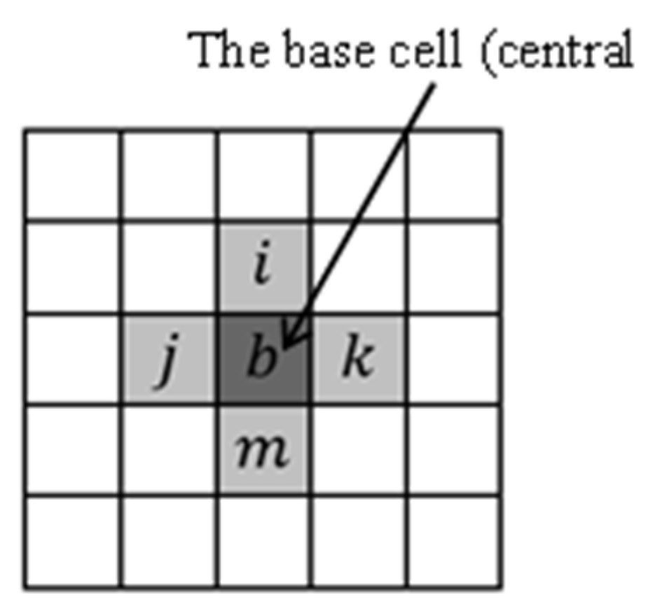
Figure 2.
Example of passive NPSF fault.
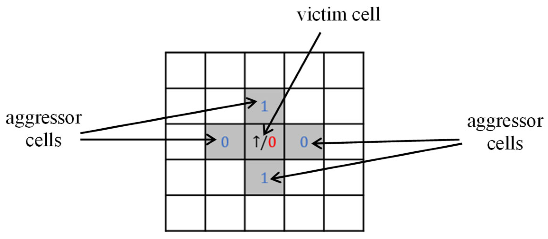
Figure 3.
Example of active NPSF fault.
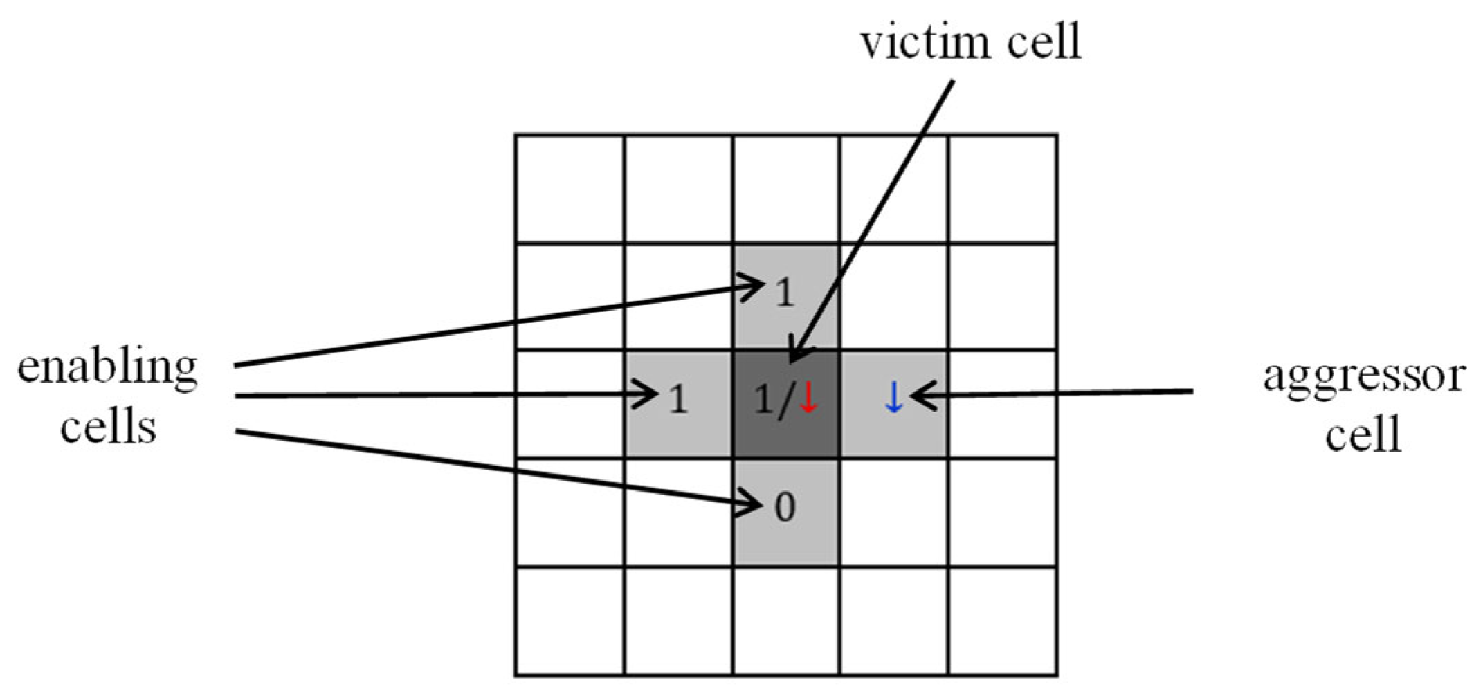
Figure 4.
march memory test.

Figure 5.
Memory initialization patterns used by the multirun march test
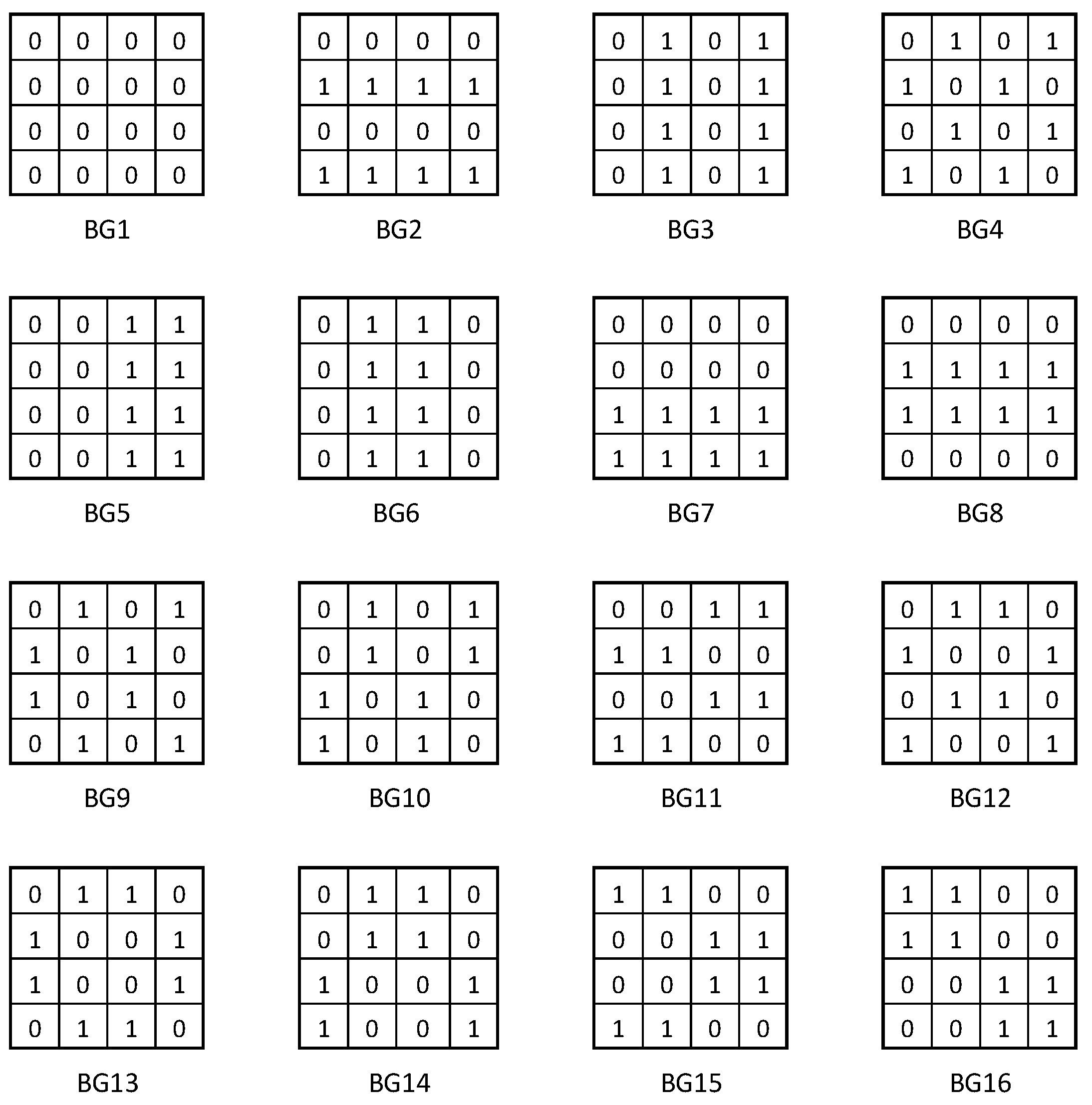
Figure 6.
Division of memory cells and the -groups of cells, respectively, into 16 classes.
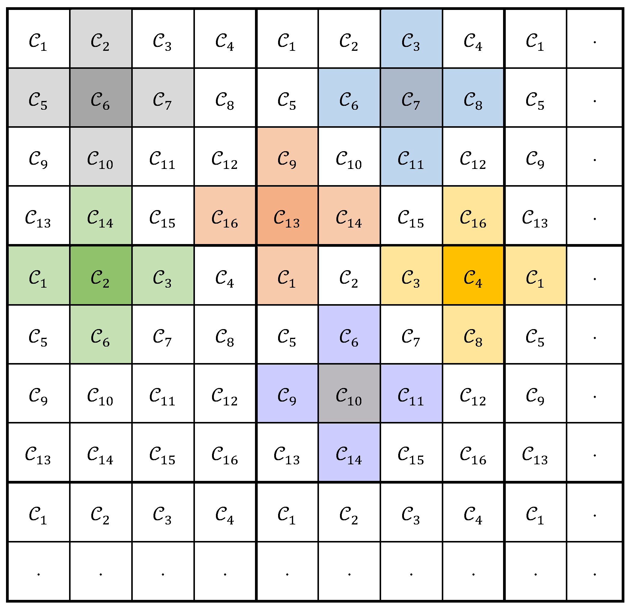
Figure 7.
The initial and complementary states, expressed in hexadecimal as / for two groups of cells of classes (light yellow) and (dark yellow), depending on data background: BG.
Figure 7.
The initial and complementary states, expressed in hexadecimal as / for two groups of cells of classes (light yellow) and (dark yellow), depending on data background: BG.
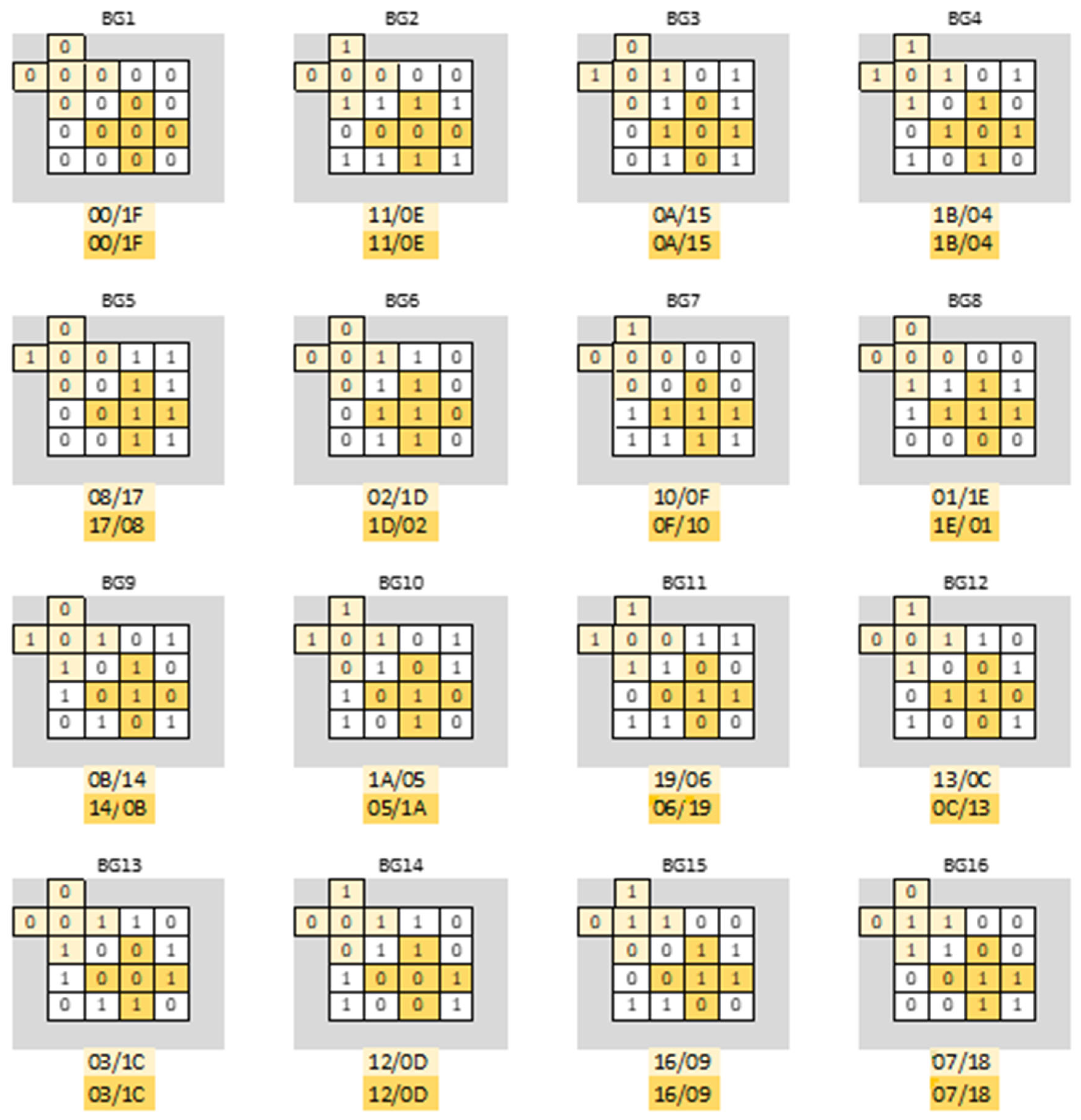
Figure 8.
The transitions performed in a group of 5 cells of class in the first 6 of the 16 iterations. of the memory test.
Figure 8.
The transitions performed in a group of 5 cells of class in the first 6 of the 16 iterations. of the memory test.
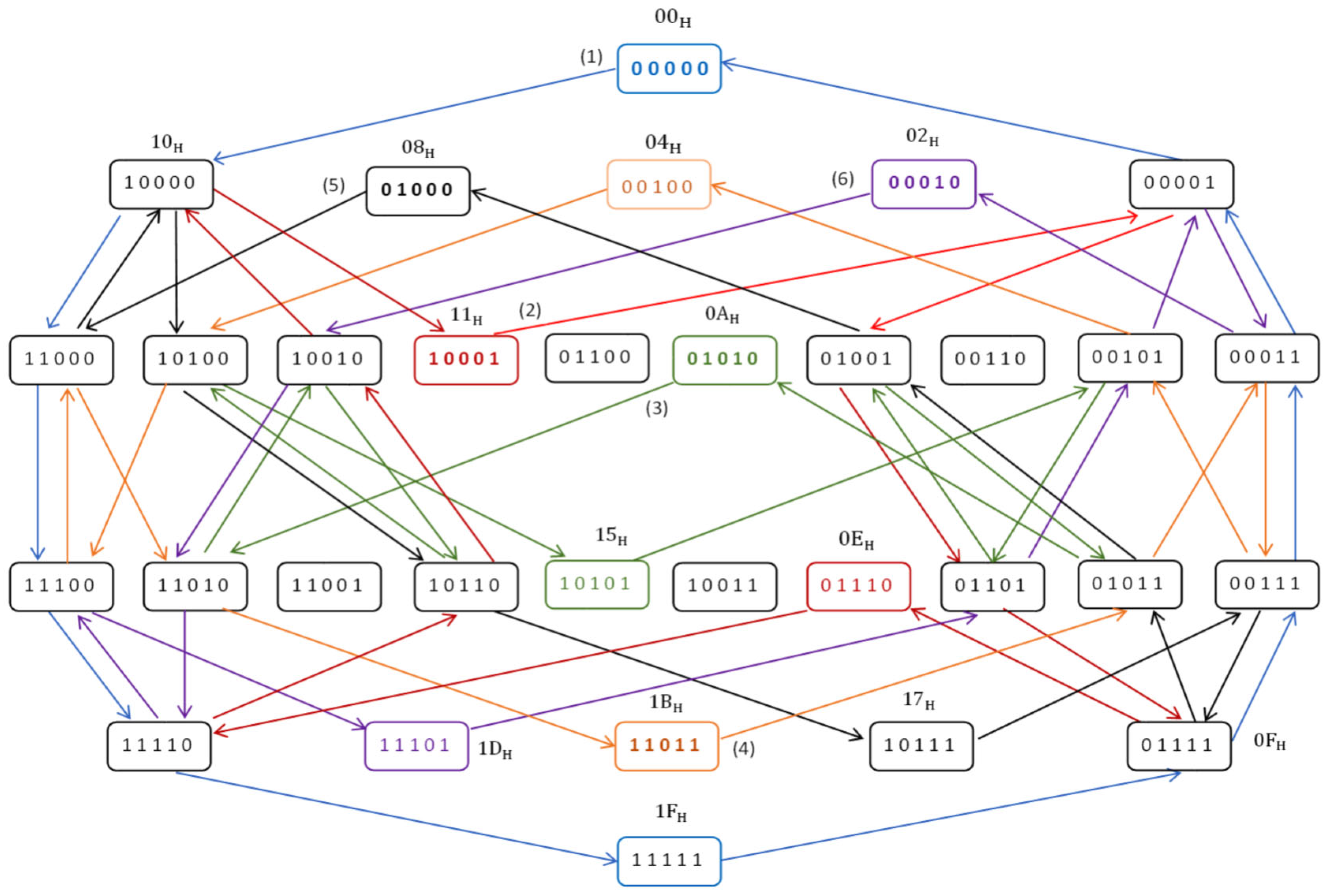
Figure 9.
The state evolution for a group of cells by applying the march element starting from different initial states, and .
Figure 9.
The state evolution for a group of cells by applying the march element starting from different initial states, and .
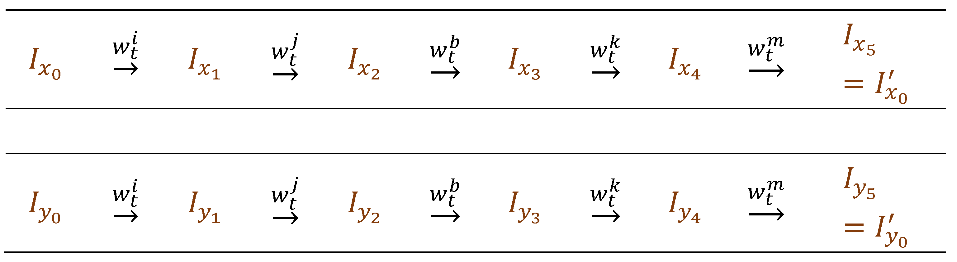
Figure 10.
The operations carried out in a group of cells when applying. the memory test.
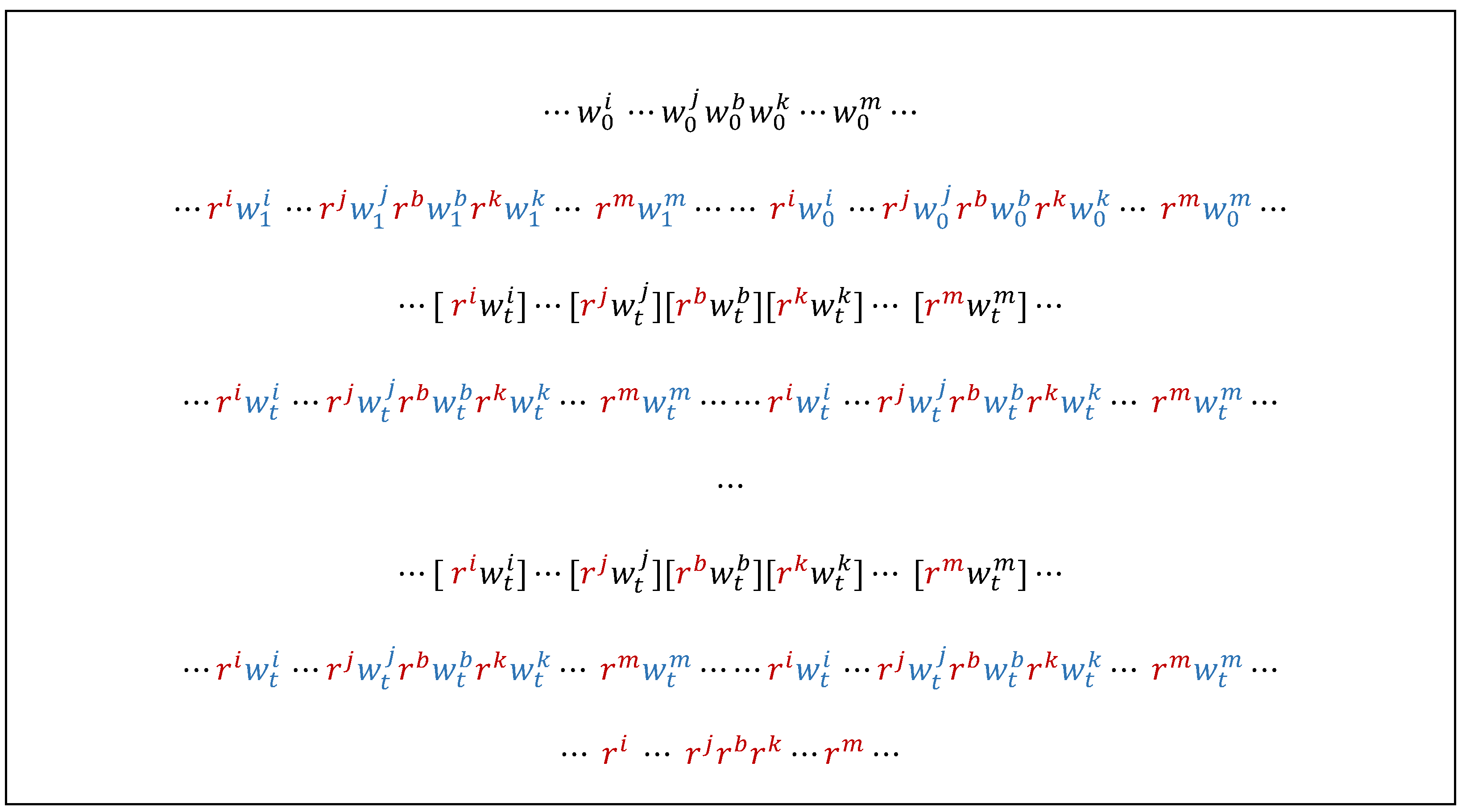
Figure 11.
march memory test.

Figure 12.
Data generation logic for the memory test.
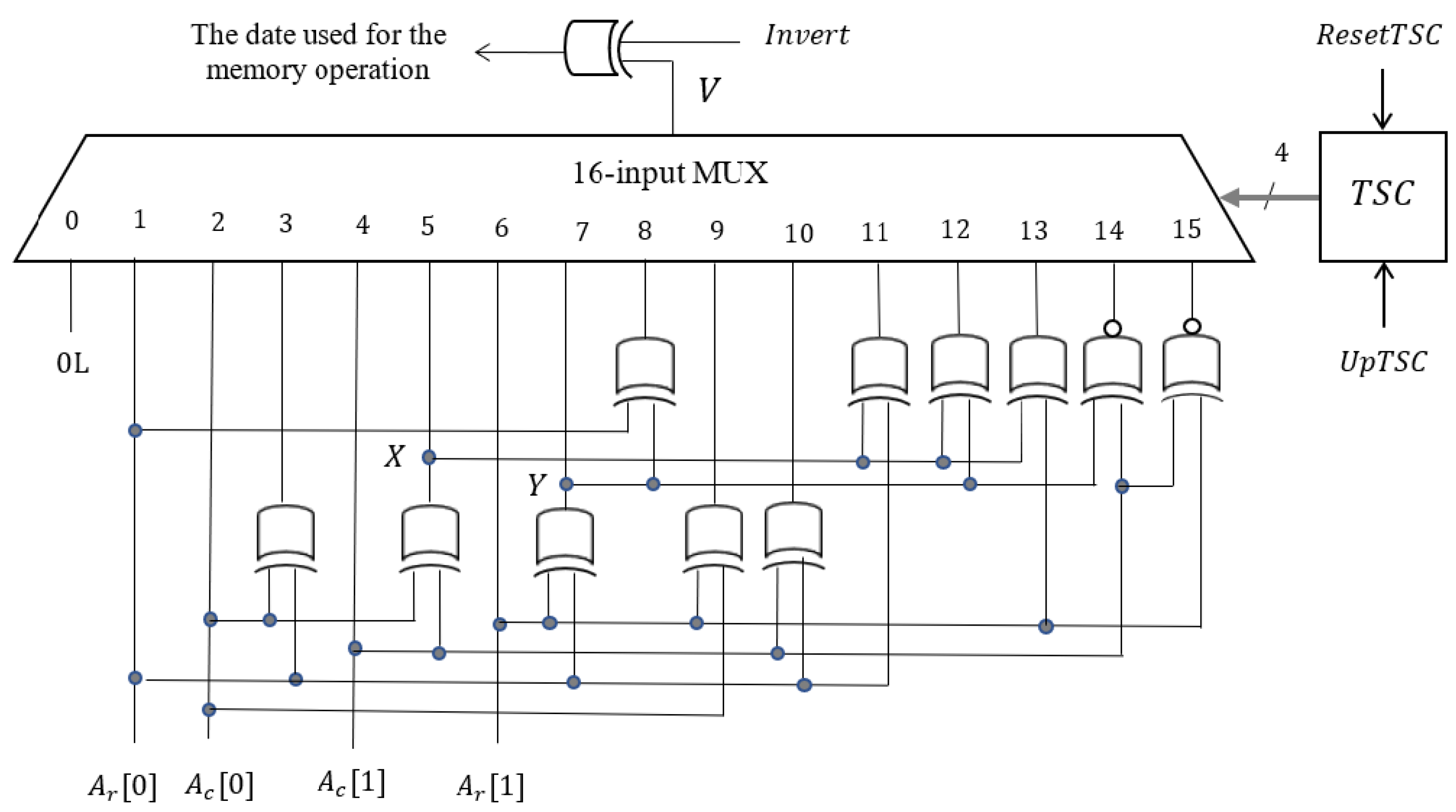
Figure A1.
CLC1 combinational logic.
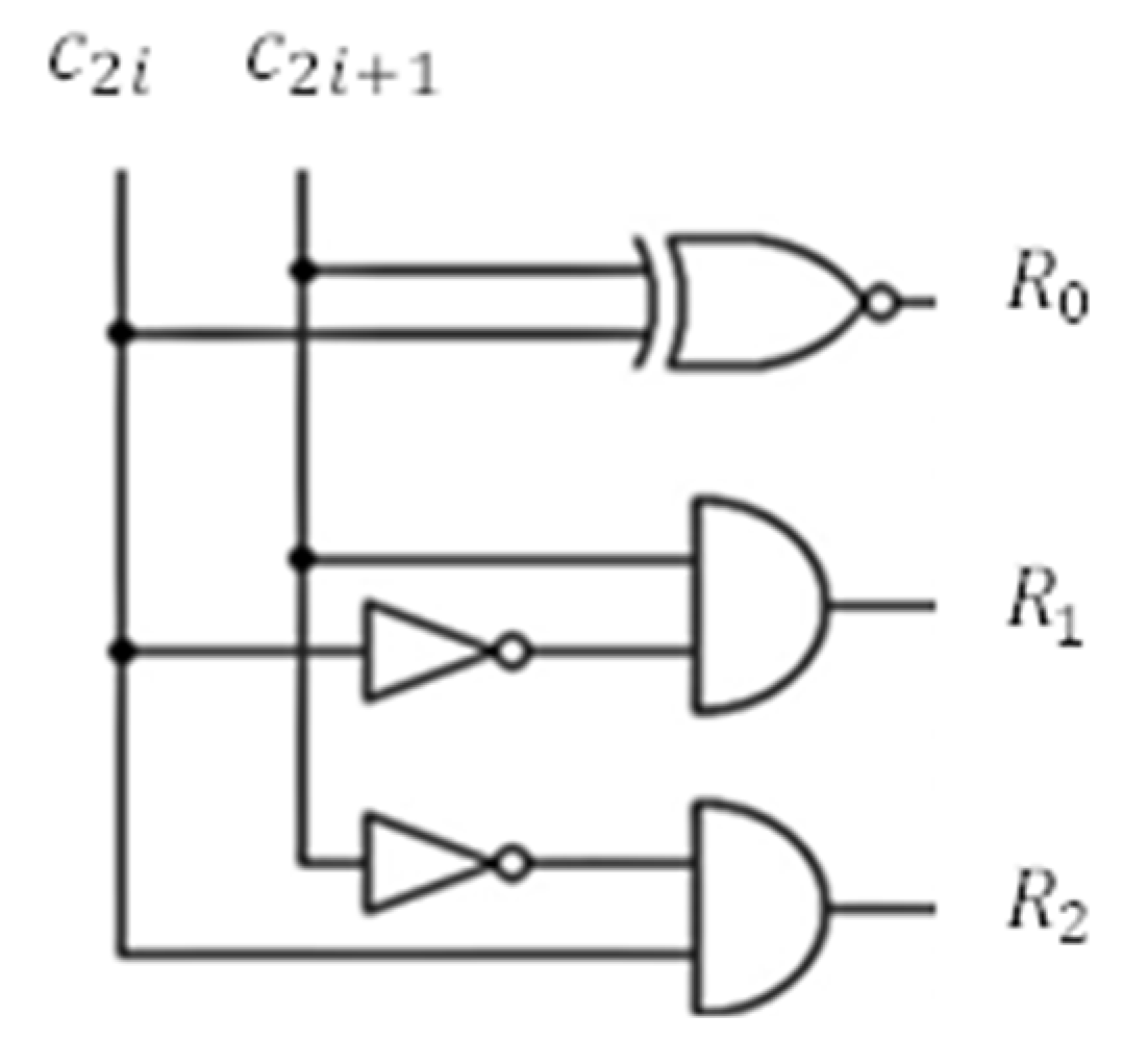
Figure A2.
Processing the values obtained from two basic CLC1 logics.
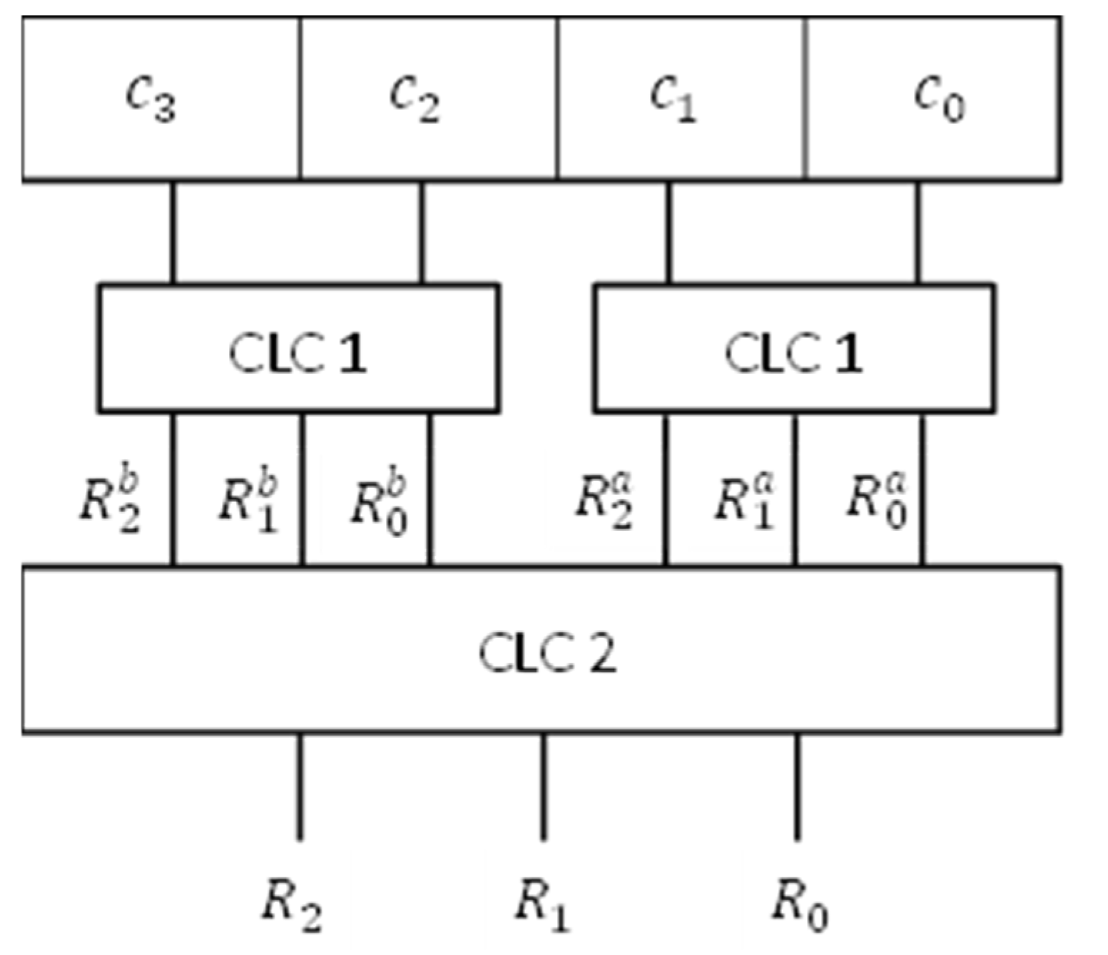
Figure A3.
combinational logic.
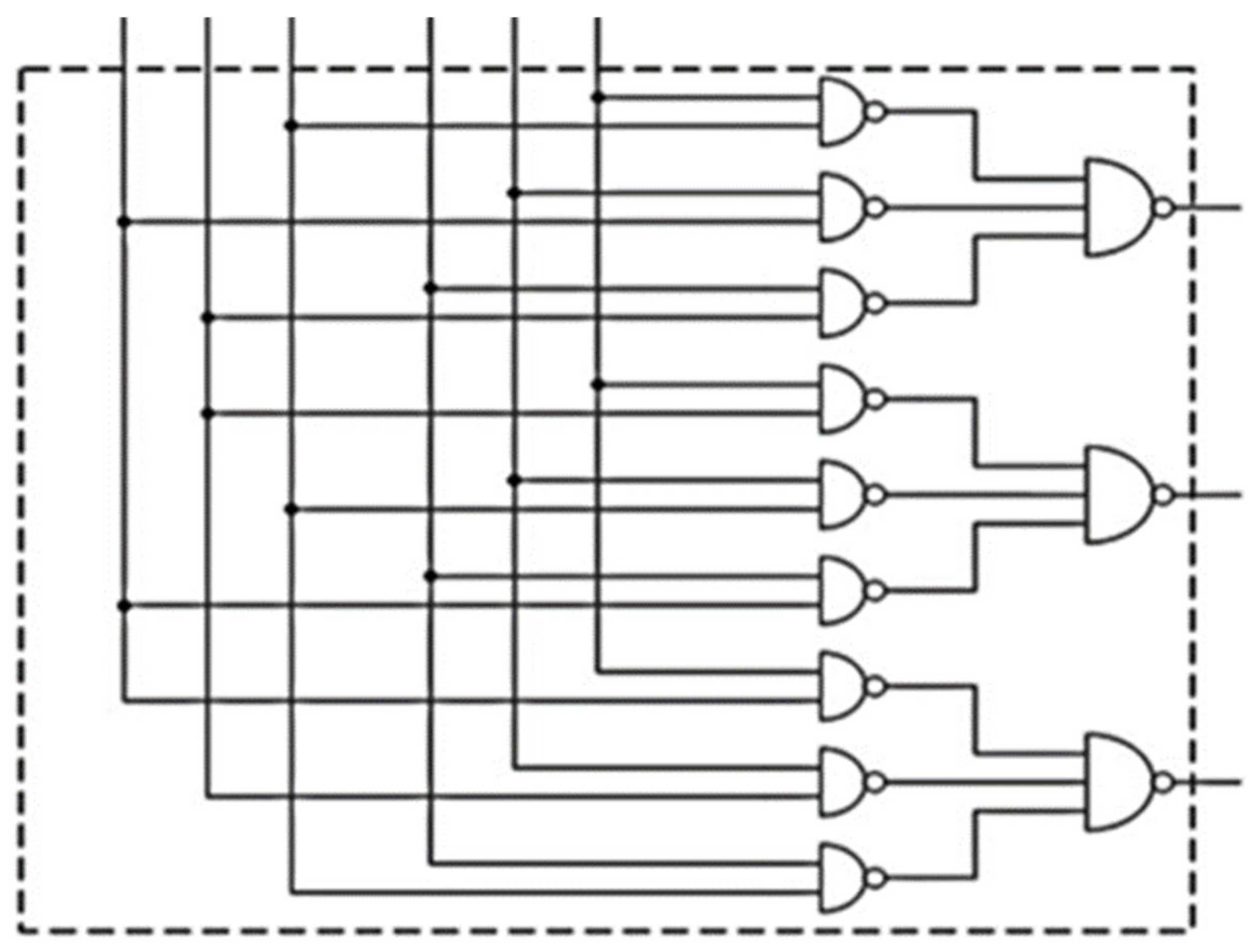
Figure A4.
Example of a series-parallel structure for calculating the value.
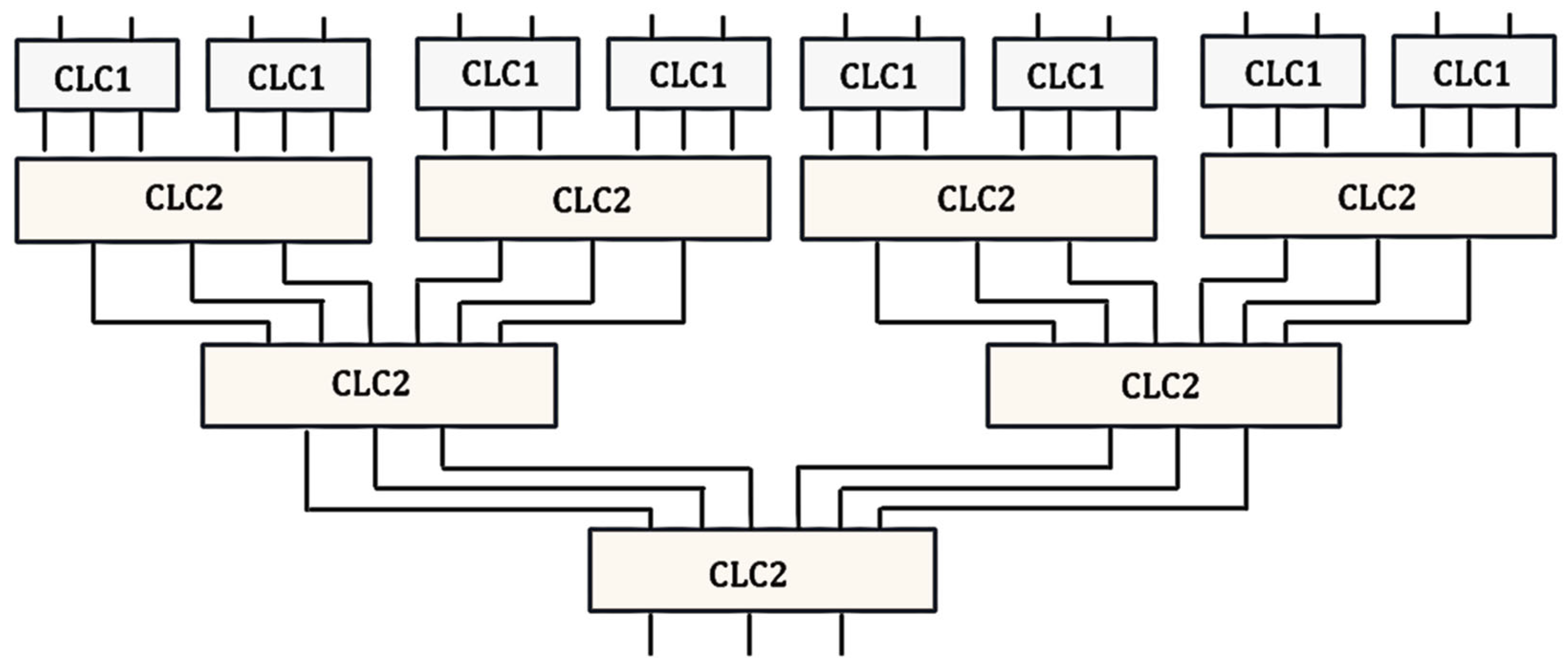
Table 1.
Dividing cells into classes by row and column addresses.
| 0 | 1 | 2 | 3 | ||
| 0 | |||||
| 1 | |||||
| 2 | |||||
| 3 | |||||
Table 2.
The initial and complementary states for a -group of cells. depending on data background and the class of which the group belongs.
Table 2.
The initial and complementary states for a -group of cells. depending on data background and the class of which the group belongs.
| BG1 | 00 | 00 | 00 | 00 | 00 | 00 | 00 | 00 | 00 | 00 | 00 | 00 | 00 | 00 | 00 | 00 |
| 1F | 1F | 1F | 1F | 1F | 1F | 1F | 1F | 1F | 1F | 1F | 1F | 1F | 1F | 1F | 1F | |
| BG2 | 11 | 11 | 11 | 11 | 0E | 0E | 0E | 0E | 11 | 11 | 11 | 0E | 0E | 11 | 0E | 0E |
| 0E | 0E | 0E | 0E | 11 | 11 | 11 | 11 | 0E | 0E | 0E | 11 | 11 | 0E | 11 | 11 | |
| BG3 | 0A | 15 | 0A | 15 | 0A | 15 | 0A | 15 | 0A | 0A | 0A | 15 | 0A | 15 | 0A | 15 |
| 15 | 0A | 15 | 0A | 15 | 0A | 15 | 0A | 15 | 15 | 15 | 0A | 15 | 0A | 15 | 0A | |
| BG4 | 1B | 04 | 1B | 04 | 04 | 1B | 04 | 1B | 1B | 04 | 1B | 04 | 04 | 1B | 04 | 1B |
| 04 | 1B | 04 | 1B | 1B | 04 | 1B | 04 | 04 | 1B | 04 | 1B | 1B | 04 | 1B | 04 | |
| BG5 | 08 | 02 | 07 | 1D | 08 | 02 | 17 | 1D | 08 | 02 | 17 | 1D | 08 | 02 | 17 | 1D |
| 17 | 1D | 08 | 02 | 17 | 1D | 08 | 02 | 17 | 1D | 08 | 02 | 17 | 1D | 08 | 02 | |
| BG6 | 02 | 17 | 1D | 08 | 02 | 17 | 1D | 08 | 02 | 17 | 1D | 08 | 02 | 17 | 1D | 08 |
| 1D | 08 | 02 | 17 | 1D | 08 | 02 | 17 | 1D | 08 | 02 | 17 | 1D | 08 | 02 | 17 | |
| BG7 | 10 | 10 | 10 | 10 | 01 | 01 | 01 | 01 | 0F | 0F | 0F | 0F | 1E | 1E | 1E | 1E |
| 0F | 0F | 0F | 0F | 1E | 1E | 1E | 1E | 10 | 10 | 10 | 10 | 01 | 01 | 01 | 01 | |
| BG8 | 01 | 01 | 01 | 01 | 0F | 0F | 0F | 0F | 1E | 1E | 01 | 1E | 10 | 10 | 10 | 10 |
| 1E | 1E | 1E | 1E | 10 | 10 | 10 | 10 | 01 | 01 | 1E | 01 | 0F | 0F | 0F | 0F | |
| BG9 | 0B | 14 | 0B | 14 | 05 | 1A | 05 | 1A | 14 | 0B | 14 | 0B | 1A | 05 | 1A | 05 |
| 14 | 0B | 14 | 0B | 1A | 05 | 1A | 05 | 0B | 14 | 0B | 14 | 05 | 1A | 05 | 1A | |
| BG10 | 1A | 05 | 1A | 05 | 0B | 14 | 0B | 14 | 05 | 1A | 05 | 1A | 14 | 0B | 14 | 0B |
| 05 | 1A | 05 | 1A | 14 | 0B | 14 | 0B | 1A | 05 | 1A | 05 | 0B | 14 | 0B | 14 | |
| BG11 | 19 | 13 | 06 | 0C | 06 | 0C | 19 | 13 | 19 | 13 | 06 | 0C | 06 | 0C | 19 | 13 |
| 06 | 0C | 19 | 13 | 19 | 13 | 06 | 0C | 06 | 0C | 19 | 13 | 19 | 13 | 06 | 0C | |
| BG12 | 13 | 06 | 0C | 19 | 0C | 19 | 13 | 06 | 13 | 06 | 0C | 19 | 0C | 19 | 13 | 06 |
| 0C | 19 | 13 | 06 | 13 | 06 | 0C | 19 | 0C | 19 | 13 | 06 | 13 | 06 | 0C | 19 | |
| BG13 | 03 | 16 | 1C | 09 | 0D | 18 | 12 | 07 | 1C | 09 | 03 | 16 | 12 | 07 | 0D | 18 |
| 1C | 09 | 03 | 16 | 12 | 07 | 0D | 18 | 03 | 16 | 1C | 09 | 0D | 18 | 12 | 07 | |
| BG14 | 12 | 07 | 0D | 18 | 03 | 16 | 1C | 09 | 0D | 18 | 12 | 07 | 1C | 09 | 03 | 16 |
| 0D | 18 | 12 | 07 | 1C | 09 | 03 | 16 | 12 | 07 | 0D | 18 | 03 | 16 | 1C | 09 | |
| BG15 | 16 | 1C | 09 | 03 | 18 | 12 | 07 | 0D | 09 | 03 | 16 | 1C | 07 | 0D | 18 | 12 |
| 09 | 03 | 16 | 1C | 07 | 0D | 18 | 12 | 16 | 1C | 09 | 03 | 18 | 12 | 07 | 0D | |
| BG16 | 07 | 0D | 18 | 12 | 16 | 1C | 09 | 03 | 18 | 12 | 07 | 0D | 09 | 03 | 16 | 1C |
| 18 | 12 | 07 | 0D | 09 | 03 | 16 | 1C | 07 | 0D | 18 | 12 | 16 | 1C | 09 | 03 | |
| Fulfillment of equation (5) |
Table 3.
The intermediate states illustrated in Figure 9.
Table 3.
The intermediate states illustrated in Figure 9.
Table 4.
Initialization value of a memory cell depending on the address.
|
Table A2.
Truth table for logical variables
| 0 | 0 | 1 | 0 | 0 |
| 0 | 1 | 0 | 0 | 1 |
| 1 | 0 | 0 | 1 | 0 |
| 1 | 1 | 1 | 0 | 0 |
Disclaimer/Publisher’s Note: The statements, opinions and data contained in all publications are solely those of the individual author(s) and contributor(s) and not of MDPI and/or the editor(s). MDPI and/or the editor(s) disclaim responsibility for any injury to people or property resulting from any ideas, methods, instructions or products referred to in the content. |
© 2025 by the authors. Licensee MDPI, Basel, Switzerland. This article is an open access article distributed under the terms and conditions of the Creative Commons Attribution (CC BY) license (http://creativecommons.org/licenses/by/4.0/).
Copyright: This open access article is published under a Creative Commons CC BY 4.0 license, which permit the free download, distribution, and reuse, provided that the author and preprint are cited in any reuse.


