
Submitted:
30 June 2025
Posted:
02 July 2025
You are already at the latest version
Abstract
In this work, reproducible routines were established for the processing of regular submi-cron-scale patterns in polymeric thin films using scanning probe lithography (one of the operating modes of a scanning probe microscope – SPM). Silicon probes were used to make the hole arrays in dynamic plowing mode. Afterwards, the tip was changed to view the arrays in intermittent contact mode. The routines were applied to PMMA thin films of different thicknesses, deposited by spin coating, optimizing this parameter for the for-mation of arrays in form of hole grid. The diameter and depth of the holes and also the height and width of the deformations to its outskirts were investigated as a function of the interaction force and the probe action time, as well of the thickness of polymer films.
Keywords:
nanostructured patterns
; thin polymer films
; PMMA
; scanning probe lithography
1. Introduction
In recent years, the scientific community has made many efforts to manipulate and understand matter on scales more close to that of the atom. Some tools have helped and continue to help humanity evolve in this understanding, one of which is the scanning probe microscope (SPM).
After its creation in 1981 [1], SPM has been used to acquire knowledge of the structure, molecular and atomic organization of surfaces in the fields of physics, chemistry and biology, contributing to scientific and technological development. At the same time, SPM has emerged as an essential tool for nanofabrication, especially for directly inducing modifications on a surface at a precise location [2]. A wide variety of methods exploiting the nanometric resolution of SPM (atomic force and scanning tunneling microscopy) have been investigated. These methods are based on the local modification of surfaces or thin films through oxidation [3,4], electronic exposure [5,6,7], force application by a probe [8,9,10,11,12] or multi probes [13], material deposition [14,15,16] or chemical etching [17].
For several areas of knowledge such as electronics, medicine and even the pharmaceutical industry, the miniaturization of devices and components is extremely important, and nanofabrication, which aims to build structures with nanoscale characteristics, can make this miniaturization viable at a relatively low cost [18,19].
Most of the current technologies used in industry for nanofabrication have evolved from conventional lithographic processes, which were developed for the semiconductor industry for the fabrication of microelectronic circuits and components [20]. However, such processes are reaching their limits and the demand for new resources for building nanoscale devices is increasing. Thus, technologies based on scanning probe microscopy have become increasingly popular, due to their great potential to fabricate and manipulate structures with sizes smaller than 100 nanometers.
One of the techniques available in SPMs, and which was used in this work, is atomic force lithography, in which the direct action of a thin probe causes nanometric modifications on the sample surface in a very precise way. This technique is used in the manufacture of lithographic masks [8,20], in the deposition of material on surfaces [14,15,16] and in the construction of molecular arrangements [21], for example.
Thus, the aim of this work was to establish reproducible routines of submicrometric patterns in polymeric thin films, using scanning probe lithography. To this, the basic parameters that optimize such routines were first studied and determined. Therefore, the diameter and depth of the holes and also the height and width of the deformations to its outskirts were investigated as a function of the interaction force and the probe action time, as well of the thickness of polymer films.
2. Materials and Methods
2.1. PMMA Thin Films Deposition
The polymer used in this work was the poly(methyl methacrylate) (PMMA) with molecular weight of 132000 u, commercially known as acrylic. This polymer is widely used as a photoresist in many device manufacturing processes. The deposition was carried out using a process known as spin coating. This method is widely used to deposit very thin layers of various materials uniformly onto smooth surfaces. According to Figure 1, the spin coating process consists of placing a certain amount of solution (containing the polymer that will form the film) on the substrate, as Figure 1a. Next, the substrate is placed in rotation at high angular speed, together with the platform that supports it (Figure 1b), so that the solution is spread and the solvent evaporates (Figure 1c).
To obtain films of different thicknesses, there are two parameters that can be varied, the angular speed of the turntable and the concentration of the solution to be deposited. In this work, the concentration of the solution was varied to obtain thin films of different thicknesses.
Thus, the films were obtained from the dissolution of different quantities of mass of the monodisperse molecular powder in the anisole solvent. Once the solution (solvent + polymer) was prepared, it was centrifuged at a speed of 5000 rpm for approximately 3 minutes, in order to separate possible particulates from the solution.
Films depositions were performed by pouring 180 ml of solution onto a 2 cm x 2 cm silicon substrate. The platform was then rotated at a maximum speed of 2500 rpm for 45 s. The Table 1 shows the values of the concentrations of the solutions and the resulting thicknesses.
2.2. Nanoestructuring Processes and Image Acquisition
The surfaces nanostructuring was performed using a scanning probe microscope (SPM) belonging to the Magnetism Laboratory (LAM) of the Physics Institute of the Federal University of Rio Grande do Sul (UFRGS). This Multimode model equipment, manufactured by Digital Instruments (DI), is equipped with the NanoScope IIIa controller interface and operated using software version 4.23r6 developed by Digital Instruments. In the microscope used, the component responsible for the sample movements during the nanostructuring and image acquisition processes is a tube-shaped piezoelectric ceramic (the scanner). For the processes performed in the present work, a scanner with wide horizontal scanning (125 µm X 125 µm) was employed.
In the nanostructuring and image acquisition processes, conventional silicon tips manufactured by BudgetSensors were employed. These tips are typically used in the intermittent contact mode imaging process of an AFM. Figure 2 shows a scanning electron microscopy (SEM) image of a silicon tip with a final radius of approximately 10 nm, located at the end of a rod. According to the manufacturer's catalog, the cantilevers employed in this work have resonance frequencies of approximately 300 kHz and can oscillate between 200 kHz and 400 kHz, corresponding to spring constants of the rods ranging from 20 N/m to 75 N/m. The radius at the apex of the tips used is less than 10 nm.
The nanostructuring process of the polymeric surfaces was carried out using the dynamic plowing technique, in the intermittent contact mode of the atomic force microscope (AFM). The experiments were performed at room temperature and in contact with air.
In dynamic plowing, the force applied by the tip on the sample surface is proportional to an operational parameter called the writing set point (Vw), an electric voltage parameter, which is defined by the equation:
where Vw must be a negative value with module greater than 0.01 volts, Vset point is the image set point that depends on the distance between tip and sample and A is a compensation factor to indirectly set the Vw value. The higher Vw module, the force applied by the tip to the sample surface is greater. In this work, the influence of the writing set point (Vw) on the dimensions of the cavities formed on the polymeric surfaces was studied. The Vw values chosen ranged from - 0.015 volts to - 0.03 volts.
Vw = Vset point -A,
Other extremely important parameter in the dynamic plowing structuring processes is the time interval, in seconds, that tip acts on the location where the structures are induced, called the pause time. Thus, we choose time intervals from 0.1 s to 0.5 s to study the influence of the pause on dimensions of the structures formed on the polymeric surfaces. The Figure 3 shows an AFM image of a (5 x 5) hole array performed at Vw = -0.03 V, where each line corresponds to a pause value.
The steps for creating the matrix in Figure 3 were used in all samples, with the writing set point (Vw) kept constant for each matrix and each line corresponding to a pause value between 0.1 seconds and 0.5 seconds.
Before placing the sample in the microscope, a marking was made to that the nanostructured areas could be easily visualized. Using a bistoury, were made grooves or scratches that locally removed the PMMA film without damage the silicon substrate. Through these grooves, an “X” was marked in the middle of the sample surface, which served as a reference for the location where the hole matrices would be made.
When couple the tip of the microscope to perform the lithographics, it was made to descend directly in the intersection of the grooves that make up the “X”. An optical microscope was used to check the proximity of the tip to the grooves. Figure 4 shows an AFM image of the intersection in the surface of a sample; the darker areas are the silicon substrate from which the PMMA was removed, generating the grooves. After acquiring an image similar at the Figure 4, the process to produce cavities on the PMMA surface begins.
After creating the matrices of holes, the tip used for indentation was removed and another tip was used to obtain the images. This procedure was extremely important, because the tip that interacts directly with the polymer surface during the production of the cavities is slightly damaged and suffers an accumulation of material by adhesion. Therefore, the resolution of an image obtained with this tip can be compromised. With the new tip, the system coupling procedure was restarted in the AFM imaging mode, to locate the nanostructured areas near the grooves intersection. Figure 5 shows an AFM image of a region close to a groove, where three matrices of holes were processed. After locating this region, individual images of each matrix were obtained, as in Figure 3.
The individual images of each matrix that were used to obtaining quantitative data, were made with a scanning frequency of 1Hz, horizontal scanning of 8 µm and resolution of 256 x 256 pixels.
In this work, efforts were concentrated on measuring the diameter and depth, as well the outer diameter and height of the deformations around the holes generated by the atomic force microscope probe. Figure 6a shows an AFM image with the general morphology of the nanostructures formed on the surface of the polymer films. It is possible to clearly distinguish the hole region, formed by the direct action of the tip, and the deformations in outskirts that are generated by the displacement the material of the hole. Figures 6b,c show, respectively, a topographic image and the profile section of the same hole.
3. Results and Discussion
Using the dynamic plowing technique in the intermittent contact mode of an atomic force microscope, mechanical deformations were induced on PMMA thin films surfaces. Such deformations were regularly created in hole array as shown in Figure 3. The results show the influence of the force (in this case the Vw writing set point) and the probe action time (pause) on the sizes of the holes and of surrounding deformations. Other results show the influence of film thickness on the sizes of structures generated on the polymer surface.
3.1. Influence of Pause and Writing Set Point on Dimensions of the Mechanically Induced Structures
The pause is the time interval, in seconds, that the tip remains in contact with the sample when piercing it. The set point (Vset point) is the parameter that controls the interaction force between the tip and sample surface. To study the influence of these two parameters on hole production, different pauses were used in each line of the matrix, varying from 0.1 s to 0.5 s, and the writing set point (Vw) was fixed at values of -0.015 V, -0.02 V and -0.03 V for each processed matrix. For each Vw values, three (5 x 5) hole matrices were made, generating fiveteen statistics points for each experimental condition. Figure 7 shows three images with hole arrays obtained with different writing set points. The polymer film used in this study had a thickness of 30 nm.
An important detail to be observed in Figure 7a is that generally in the 0.1 s pause no holes were generated, and thus only four lines (four pause values) were analyzed. Figure 8 shows the graphs of external and internal diameters of holes as a function of pause for the three Vw values used in this work. In these, seem that increases in the writing set point and pause time cause increases in the external and internal diameters of the deformations. The increase is approximately linear for small pauses, but there is a tendency for saturation of the external and internal diameters after pauses of 0.3-0.4 s for Vw of -0.015 V and -0.02 V. Only for Vw = -0.03 V the increase in diameters continue to be approximately linear for larger pauses.
Figure 9 shows the graphs for the heights of the left and right borders as a function of pause for the different Vw values used. The behavior observed is the same that the external and internal diameters, including the same saturation trends. However, for height right border, at Vw of -0.03 V and pause of 0.4 s, there is too a saturation tendency. The behavior differences of the borders generated on the left and right of holes, may be due to the fact that the rod of supporting the tip forms an angle with the sample surface during indentations.
Figure 10 shows a graph of the depth of the holes as a function of pause for the three Vw values. In this case, an increase in the depth holes can be observed for the three set point values up to the 0.3 s pause. After this pause value, there is no change in depth values. This occurs because the tip through pass the polymeric film and reaches the silicon that supports.
From the results presented, is possible to see that the increase in the writing set point (Vw), and so, the increase in the force applied by the tip on surface, there’s an increase in the dimensions of defects formed on polymeric surfaces. As the pause time increases, there's too an increase in the dimensions of the defects; however, from certain pause values, there's a decrease in the increment and a tendency to stabilization in the sizes of generated structures. The pause value from which growth slows down depends on the Vw value at which is operating: the higher module of Vw value, lower the pause value at which stabilization occur. This stabilization must be associated with the fact that the tip has pierced the entire polymer layer, there is no more material below to be displaced from the hole. Thus, the optimal condition for the structuring processes related to the interaction force and probe action time occurred for Vw = - 0.02 V and a pause of 0.3 s, since under these conditions the tip already pierced the polymer layer and the force applied by the probe on the sample and action time are minimized, avoiding excessive wear.
3.2. Influence of Film Thickness on Dimensions of the Mechanically Induced Structures
To study the influence of film thickness on dimensions of the deformations generated by AFM tip, the write set point was fixed at -0.02 V for each matrix and each line was generated with a pause value of 0.1 s to 0.5 s. Figure 11 evidence the strong influence of film thickness on dimensions of the structures.
Figure 12a,b show the graphs of the external and internal diameters as a function of the thickness for pauses of 0.3 s, 0.4 s and 0.5 s. Is possible to observe that for the pause 0.3 s, there's a considerable decrease in external and internal diameters among the thicknesses of 3.8 nm and 6.5 nm. For larger thicknesses, 16 nm and 30 nm, there is an increase in diameters for the same pause.
For the pause 0.4 s, between the thicknesses of 3.8 nm and 6.5 nm, there's a small increase in external diameter and a small decrease in internal diameter. Between thicknesses of 6.5 nm and 16 nm, the external diameter increases considerably and the internal diameter remains practically constant. However, between thicknesses of 16 nm and 30 nm the opposite occurs, the external diameter remains constant and the internal diameter appear a considerable increase.
For the pause of 0.5 s, there's a considerable decrease in external and internal diameters between the thicknesses of 3.8 nm and 6.5 nm, between the thicknesses of 6.5 nm and 16 nm there's a large increase in both diameters and from 16 to 30 nm in thickness, the external diameter appears a small increase while the internal diameter increases significantly.
It was expected that with increase in film thickness there would be an increase in external and internal diameters, once the thicker material layer, greater the mass displaced from cavity. However, this fact was not observed in some cases such as in the 3.8 nm and 6.5 nm thick films; this is very interesting, because for these thicknesses is possible to approximate the values for external and internal diameters, minimizing the length of borders and maximizing the diameter of holes. Here is important emphasize that the twisting effect of rod that supports the tip can have affected the results [23]. Such effect must have a considerable influence on the structuring of thinnest films, since the proximity to the substrate generates greater twists and, consequently, lateral movements of the tip that change its attack angle to the sample.
Another important detail to be highlighted is the conical shape of the tip which, together with the thickness, has a great influence on the sizes of the external and internal diameters, as well on the border heights. Since thicker the polymer film, greater the tip penetration, greater the contact area between the tip and polymer and greater the amount of material displaced.
Figure 13a,b shows the graphs of the heights of the left and right borders as a function of thickness, respectively. Is possible to observe that for all pause values, the height of the borders increases proportionally with film thickness. Also, their values are very close for all pause values.
Figure 14 shows a graph of the depth of the holes as a function of film thickness. It is evident that when piercing the films, the AFM tip comes very close to the interface between the polymer and silicon substrate, being important to highlight that the only case in which the depth of hole values were equal to the thickness occurred for the 30 nm film for all three pause values. In the other cases there is an apparent difference of approximately 2 nm, which shows that rod twist effects are important in thinner films, since was expected that the tip pierce the entire polymer layer and reach the silicon substrate.
References
- BINNIG, G.; Rohrer, H.; Gerber, Ch.; Weibel, E. Surface studies by scanning tunneling microscopy, Physical Review Letters, v. 49, p. 57-61, 1982. [CrossRef]
- KRIVOSHAPKINA, Y.; Kaestner, M.; Rangelow, I. W. ; Tip-based nanolithography methods and materials, Frontiers of Nanoscience, v. 11, p. 497-542, 2016. [CrossRef]
- SNOW, E. S.; Campbell, P. M. Fabrication of Si nanostructures with an atomic force microscope, Applied Physics Letters, v. 64, n. 15, p. 1932-1934, 1994. [CrossRef]
- CAMPBELL, P. M.; Snow, E. S. Proximal probe-based fabrication of nanostructures, Semiconductor Science and Technology, v. 11, n. 11s, p. 1558-1562, 1996. https://apps.dtic.mil/sti/pdfs/ADA360216.
- HIRONAKA, K.; Aoki, K.; Hori, H.; Yamada, S. Nano-Fabrication on GaAs Surface by Resist Process with Scanning Tunneling Microscope Lithography, Japanese Journal of Applied Physics, v. 36, n. 6B, p. 3839-3843, 1997. https://iopscience.iop.org/article/10.1143/JJAP.36. 3839. [Google Scholar]
- MARRIAN, C. R. K.; Dobisz, E. A. Electron-beam lithography with scanning tunneling microscope, Journal of Vacuum Science and Technology B, v. 10, n. 6, p. 2877-2881, 1992. https://zenodo. 1236. [Google Scholar]
- KRAGLER, K.; Günther, E.; Leuschner, R.; Falk, G.; Seggern, H. Low-voltage electron-beam lithography with scanning tunneling microscopy in air: A new method for producing structures with high aspect ratios, Journal of Vacuum Science and Technology B, v. 14, n. 2, p. 1327-1330, 1996. [CrossRef]
- WENDEL, M.; Irmer, B.; Cortes, J.; Kaiser, R.; Lorenz, H.; Kotthaus, J. P.; Lorke, A. Nanolithography with an atomic force microscope, Superlattices and Microstructures, v. 20, n. 3, p. 349-356, 1996. https://www.nano.physik.uni-muenchen.de/nanophysics/_assets/pdf/1996/96-30_Wendel_SuperlMicrostr.
- AVRAMESCU, A.; Uesugi, K.; Suemune, I. Atomic Force Microscope Nanolithography on SiO2/Semiconductor Surfaces. Japanese Journal of Applied Physics, v. 36, n. 6B, p. 4057-4060, 1997. https://iopscience.iop.org/article/10.1143/JJAP.36. 4057. [Google Scholar]
- KLEHN, B.; Kunze, U. Nanolithography with an atomic force microscope by means of vector-scan controlled dynamic plowing, Journal of Applied Physics, v. 85, n. 7, p. 3897-3903, 1999. [CrossRef]
- SNOW, E.S.; Campbell, P.M.; Perkins, F.K. Nanofabrication with proximal probes, Proceedings of the IEEE, v. 85, n. 4, p. 601-611, 1997. https://ieeexplore.ieee.org/stamp/stamp.jsp? 5737. [Google Scholar]
- XIE, X. N.; Chung, H. J.; Sow, C. H.; Wee, A. T. S. Nanoescale materials patterning and engineering by atomic force microscopy nanolithography, Materials Science and Engineering R, v. 54, p. 1-48, 2006. [CrossRef]
- GENG, Y.; Wang, J.; Zhang, Q.; Yan, Y. ; Liu, Y; Fabrication of periodic nanostructures for SERS substrates using multi-tip probe-based nanomachining approach, Applied Surface Science, v. 576. Part b, 2022. [CrossRef]
- MCCORD, M. A.; Kern, D. P.; Chang, T. H. P. Direct deposition of 10-nm metallic features with scanning tunneling microscope, Journal of Vacuum Science and Technology B, v. 6, n. 6, p. 1877-1880, 1988. [CrossRef]
- EHRICHS, E. E.; Silver, R. M.; Lozanne, A. L. Direct writing with the scanning tunneling microscope, Journal of Vacuum Science and Technology A, v. 6, n. 2, p. 540-543, 1988. [CrossRef]
- EHRICHS, E. E.; Yoon, S.; Lozanne, A. L. Direct writing of 10 nm features with the scanning tunneling microscope, Applied Physics Letters, v. 53, n. 23, p. 2287-2289, 1988. [CrossRef]
- KANESHIRO, C.; Okumura, T. Nanofabrication on n-GaAs surface using a scanning tunnelling microscope in a Ni-salt solution, Thin Solid Films, v. 281-282, n. 1-2, p. 606-609, 1996. [CrossRef]
- CHEN, Y.; Hsu, J.; Lin, H. Fabrication of metal nanowires by atomic force microscopy nanoscratching and lift-off process, Nanotechnology, v. 16, p. 1112-115, 2005. https://iopscience.iop.org/article/10. 1088. [Google Scholar]
- TSENG, A. A.; Notargiacomo, A.; Chen, T. P. Nanofabrication by scanning probe lithography: A review. B, 2005; 23. [Google Scholar] [CrossRef]
- WIESAUER, K.; Springholz, G. Fabrication of semiconductor nanostructures by nanoindentation of photoresist layers using atomic force microscopy. Journal of Applied Physics, v. 88, n. 12, p. 7289-7297, 2000. [CrossRef]
- WEISENHORN, A. L.; Mac Dougall, J. E.; Gould, S. A. C.; Cox, S. D.; Wise, W. S.; Massie, J.; Maivald, P.; Elings, V. B.; Stucky, G. D.; Hansma, P. K. Imaging and Manipulating Molecules on a Zeolite Surface with an Atomic Force Microscope, Science, v. 247, p. 1330-1333, 2009. https://www.science.org/doi/10.1126/science.247.4948. 1330. [Google Scholar]
- RUSSELL, P.; Batchelor, D.; Thornton, J. SEM and AFM: Complementary Techniques for High Resolution Surface Investigations, Veeco Metrology Group. https://www.researchgate. 2374. [Google Scholar]
- GENG, Y.; Yan, Y.; Wang, J.; Fang, Z.; He, Y. Implementation of AFM tip-based nanostcratching process on single crystal copper: Study of material removal state, Applied Surface Science, v. 459, p. 723-731, 2018. [CrossRef]
Figure 1.
Steps of the spin coating process.
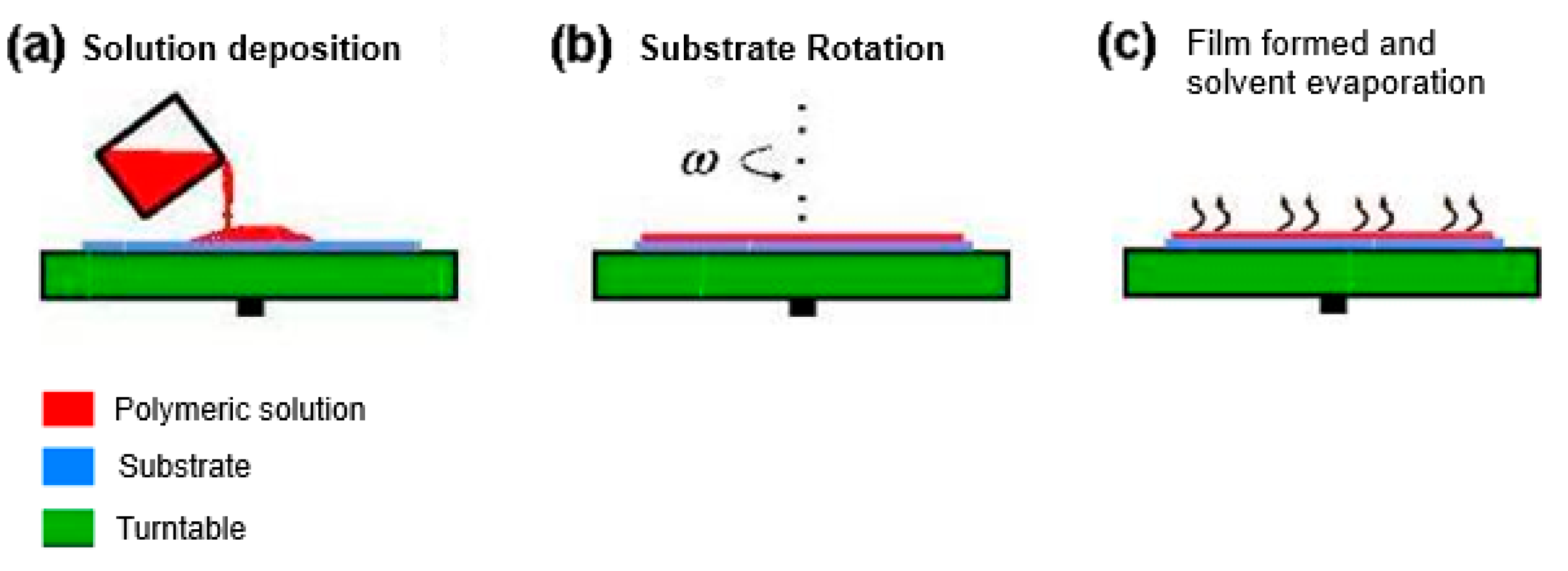
Figure 2.
Scanning electron microscopy (SEM) image of a silicon tip with a final radius about 10 nm, at the end of cantilever or rod. Scale bar = 100 µm [22].
Figure 2.
Scanning electron microscopy (SEM) image of a silicon tip with a final radius about 10 nm, at the end of cantilever or rod. Scale bar = 100 µm [22].
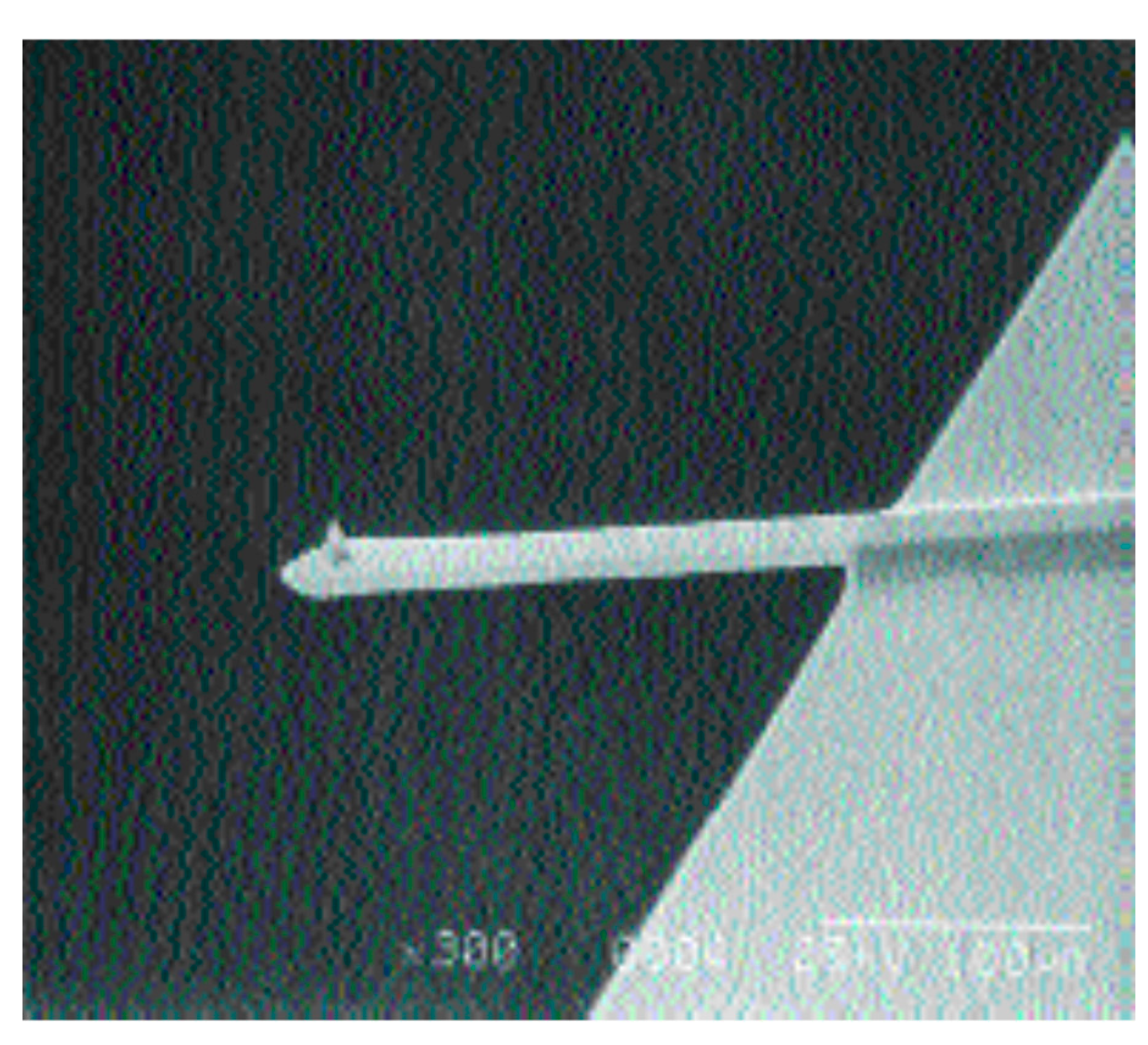
Figure 3.
AFM image of a (5 x 5) hole array performed at Vw = - 0.03 V where each line corresponds to a pause value.
Figure 3.
AFM image of a (5 x 5) hole array performed at Vw = - 0.03 V where each line corresponds to a pause value.
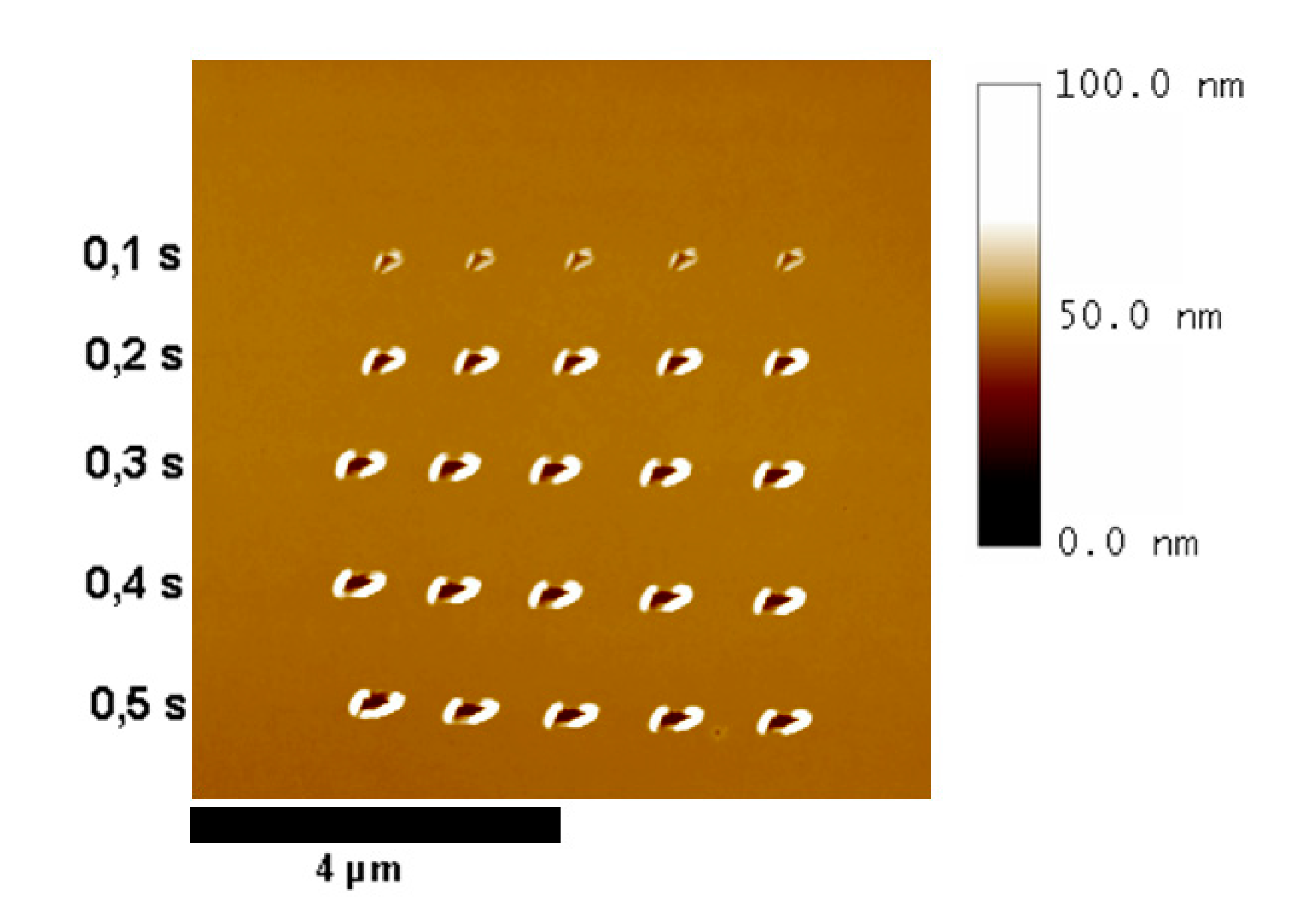
Figure 4.
AFM image of the intersection in the surface of a sample. The darker areas are the silicon substrate from which the PMMA was removed, generating the grooves.
Figure 4.
AFM image of the intersection in the surface of a sample. The darker areas are the silicon substrate from which the PMMA was removed, generating the grooves.
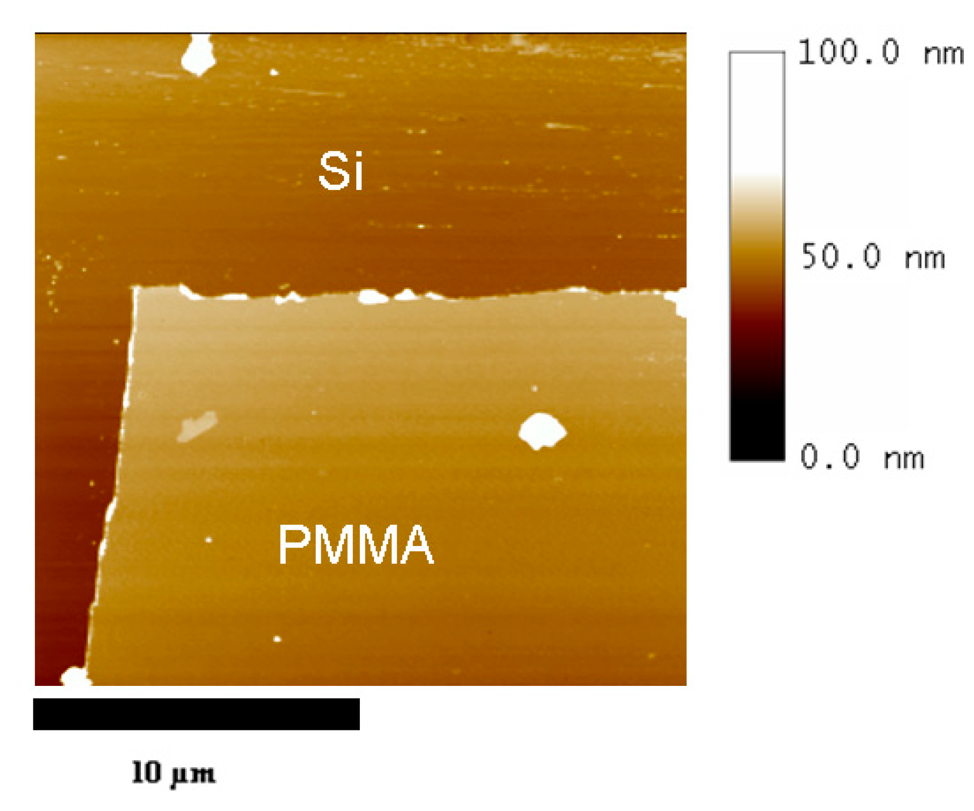
Figure 5.
AFM image of a region close to a groove, where three hole arrays were processed.
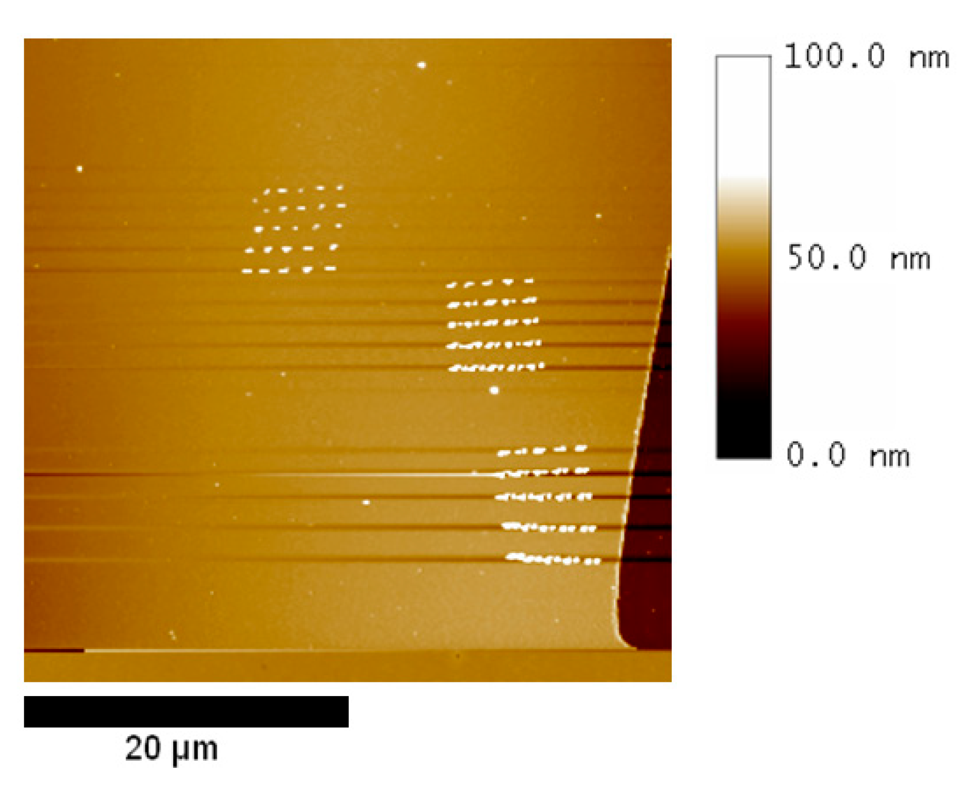
Figure 6.
AFM images showing (a) the general morphology and (b) the topography of the nanostructures generated by the tip on PMMA film surface. In (c) a profile of cross section along the nanostructure in which ED, ID, HLB, HRB and DP are, respectively, the external diameter, the internal diameter, height left border, height right border and depth of hole.
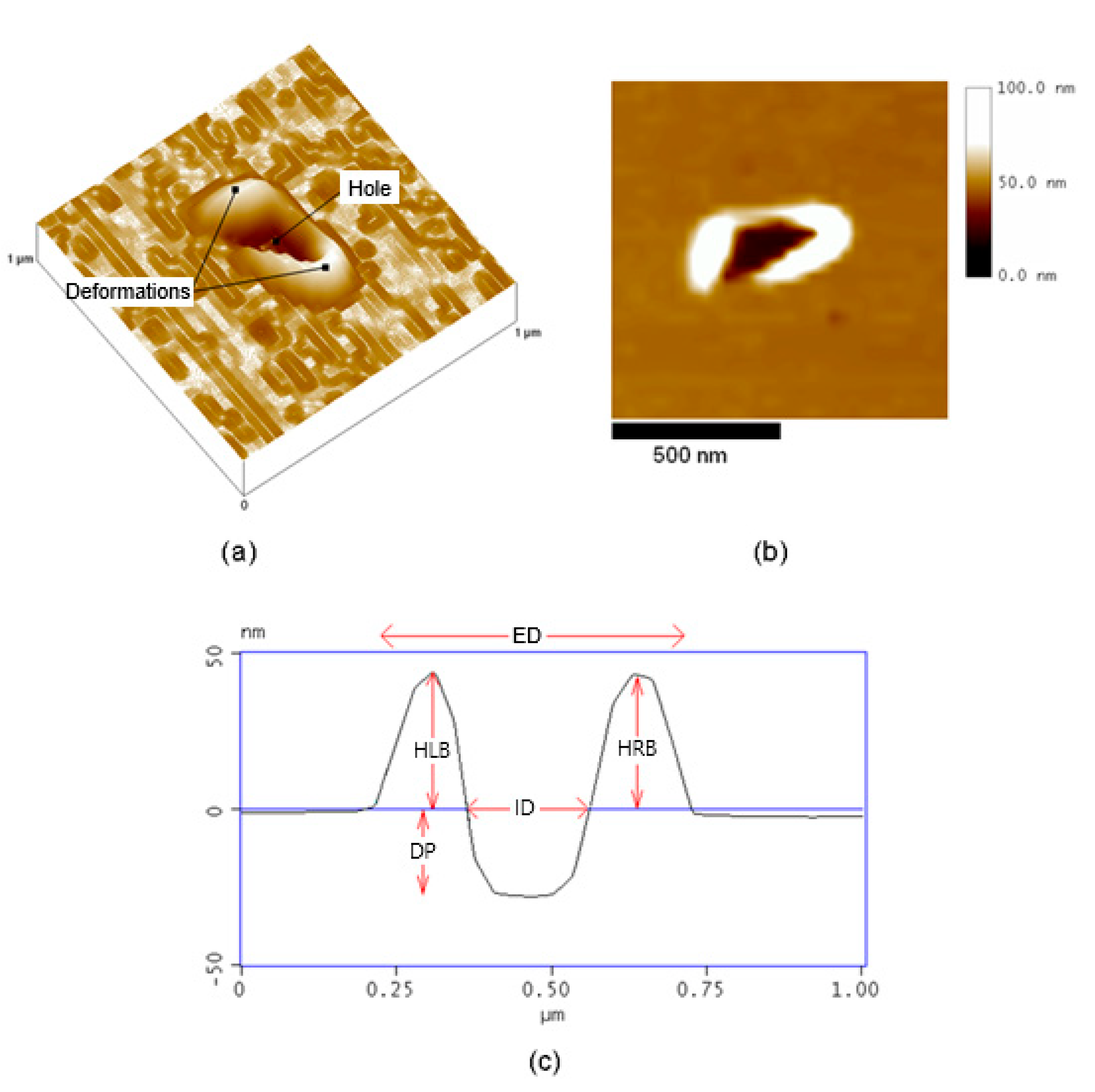
Figure 7.
AFM topographic images of hole arrays in 30 nm PMMA thin films processed with writing set points of (a) −0.015 V, (b) −0.02 V, and (c) −0.03 V. Pause times range from 0.1 s to 0.5 s from the first to the fifth line of holes in each image.
Figure 7.
AFM topographic images of hole arrays in 30 nm PMMA thin films processed with writing set points of (a) −0.015 V, (b) −0.02 V, and (c) −0.03 V. Pause times range from 0.1 s to 0.5 s from the first to the fifth line of holes in each image.
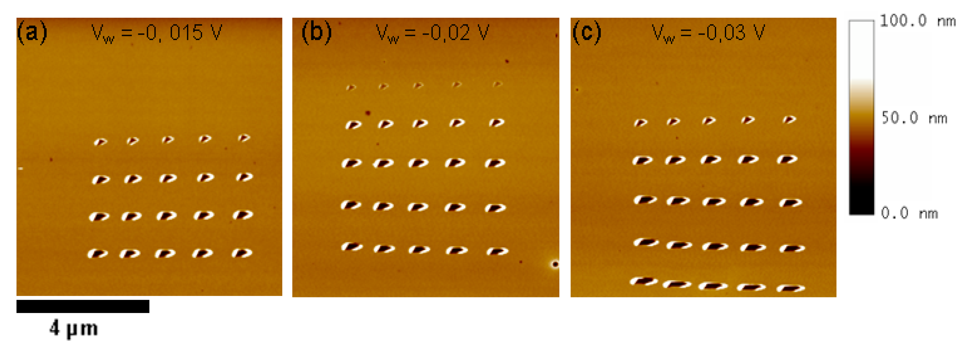
Figure 8.
External diameter (a) and internal diameter (b) as a function of pause for the three Vw values.
Figure 8.
External diameter (a) and internal diameter (b) as a function of pause for the three Vw values.
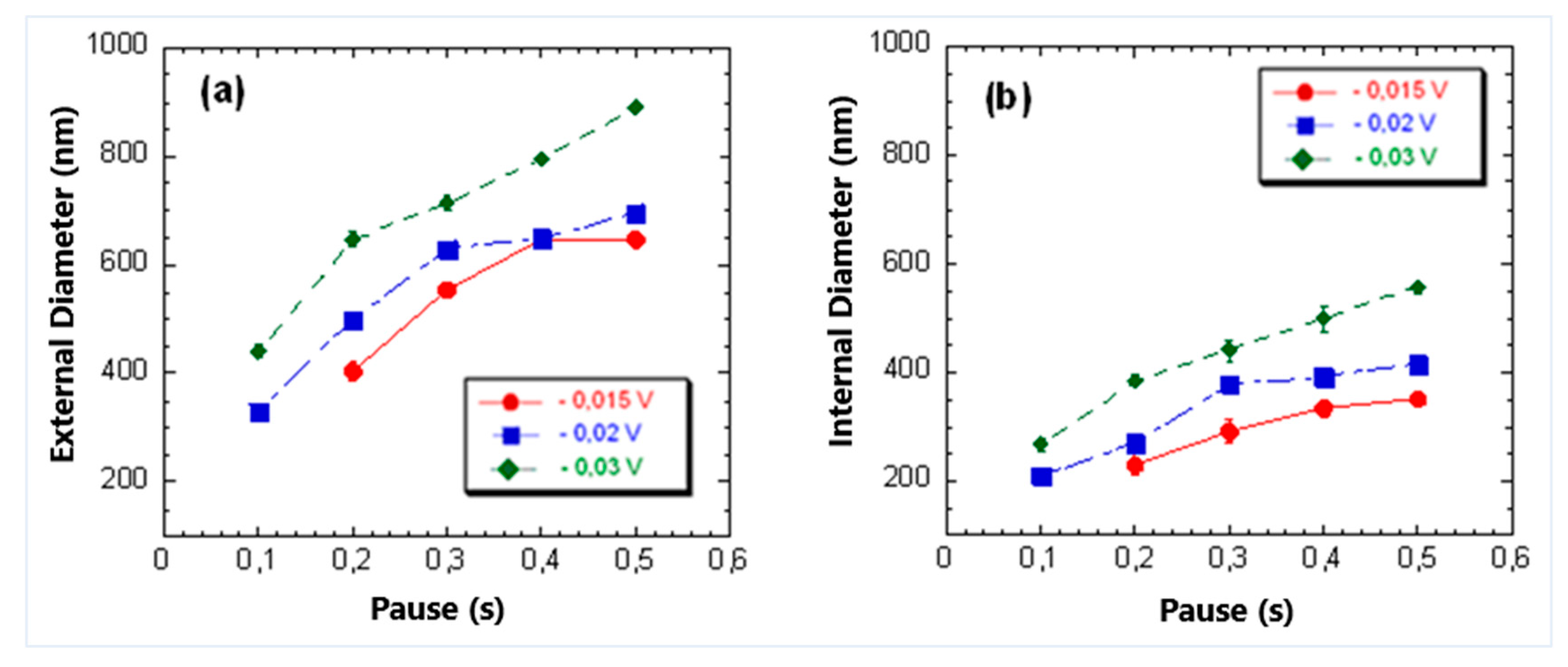
Figure 9.
Height left border (a) and height right border (b) as a function of pause for the three Vw values.
Figure 9.
Height left border (a) and height right border (b) as a function of pause for the three Vw values.
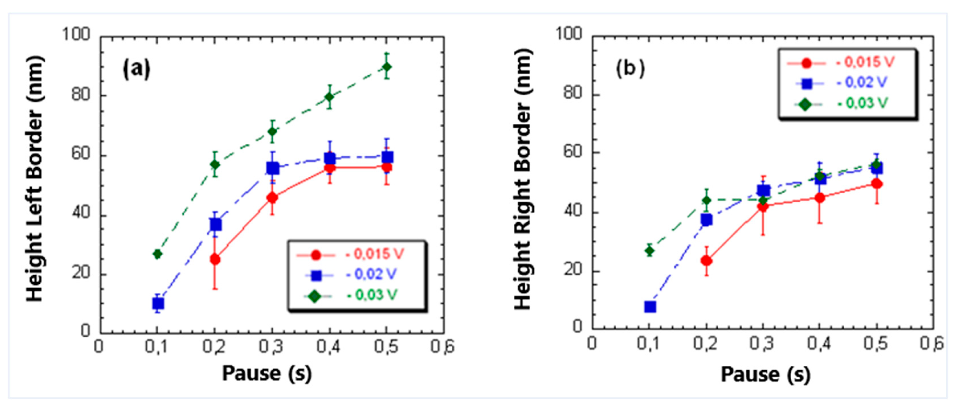
Figure 10.
Depth of holes as a function of pause for the three Vw values.
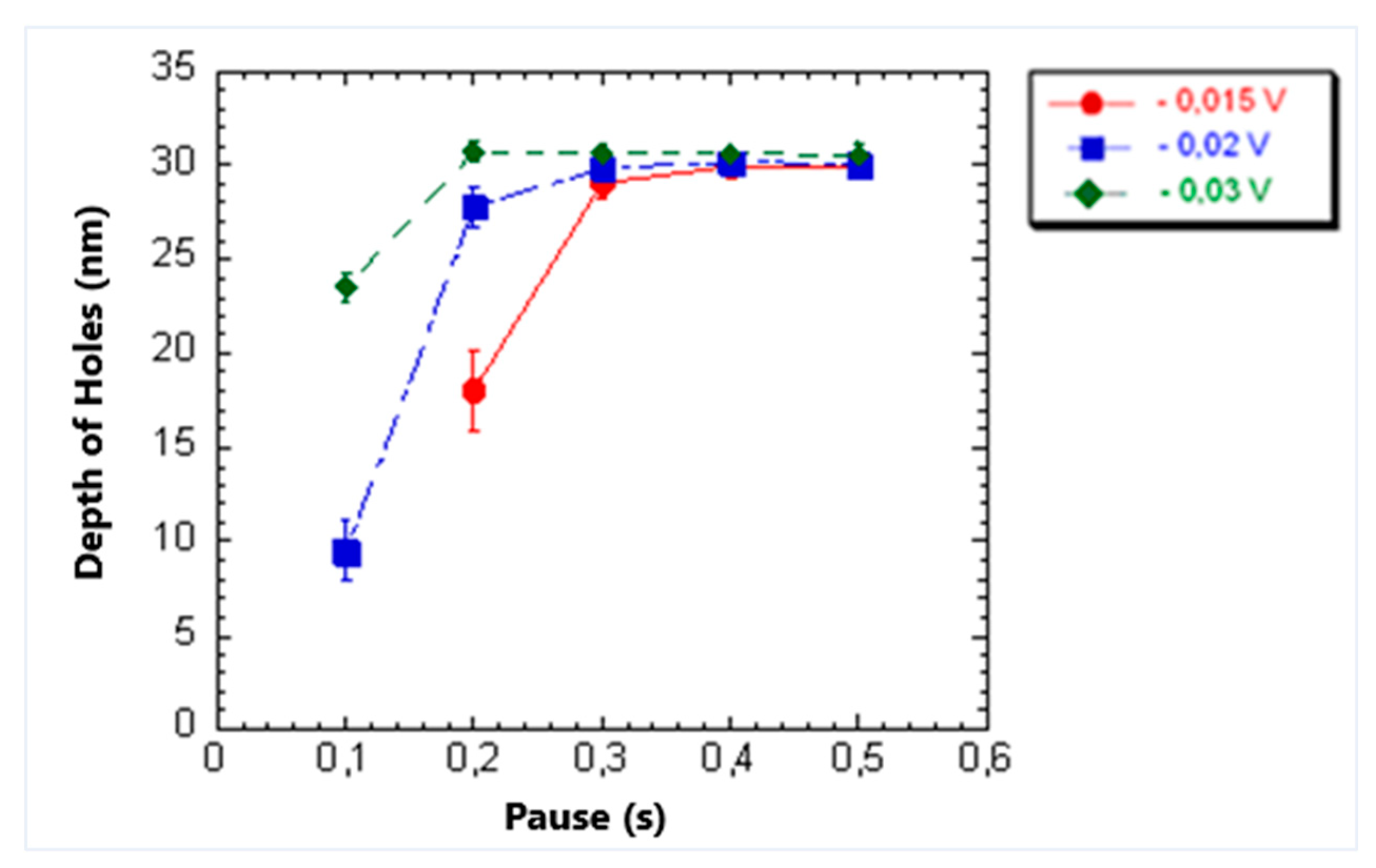
Figure 11.
AFM images of hole arrays in PMMA films of different thicknesses: (a) 3.8 nm; (b) 16 nm; and (c) 30 nm. The arrays performed at Vw = -0.02 V and each line corresponding to a pause value between 0.1 s and 0.5 s from the first to the fifth line of holes in each image.
Figure 11.
AFM images of hole arrays in PMMA films of different thicknesses: (a) 3.8 nm; (b) 16 nm; and (c) 30 nm. The arrays performed at Vw = -0.02 V and each line corresponding to a pause value between 0.1 s and 0.5 s from the first to the fifth line of holes in each image.
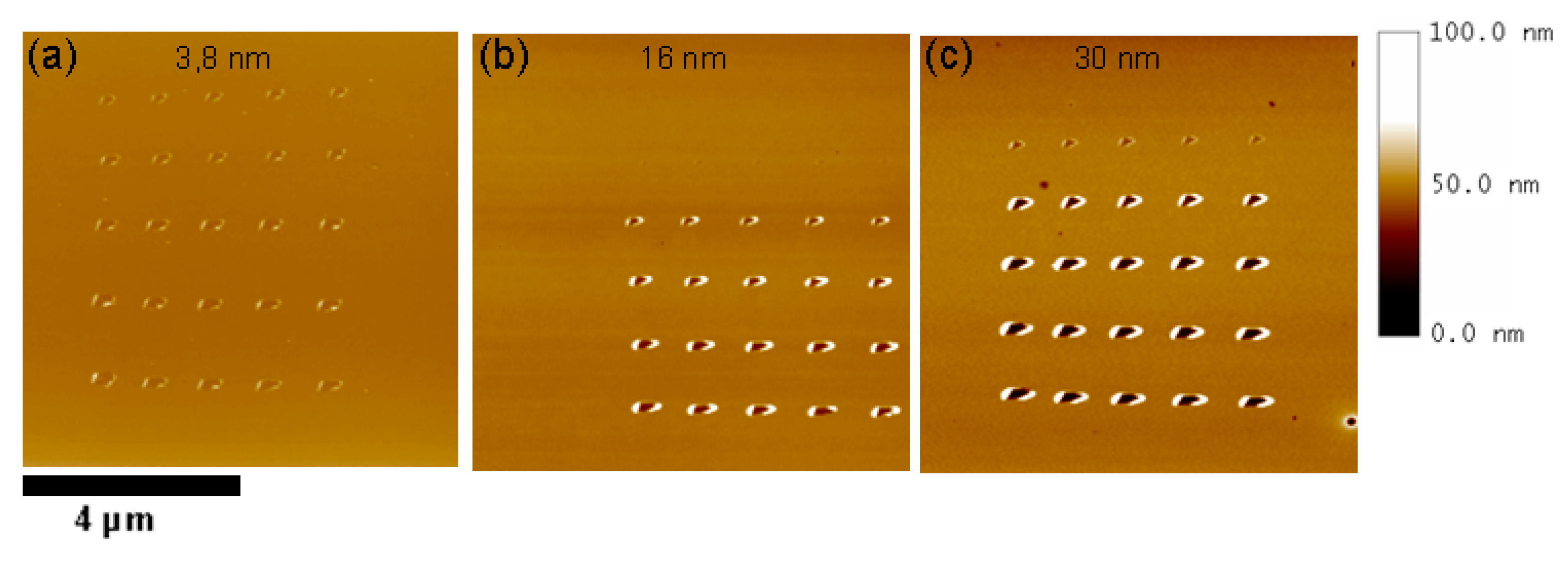
Figure 12.
External diameter (a) and internal diameter (b) as a function of thickness for pauses from 0.3 s to 0.5 s.
Figure 12.
External diameter (a) and internal diameter (b) as a function of thickness for pauses from 0.3 s to 0.5 s.
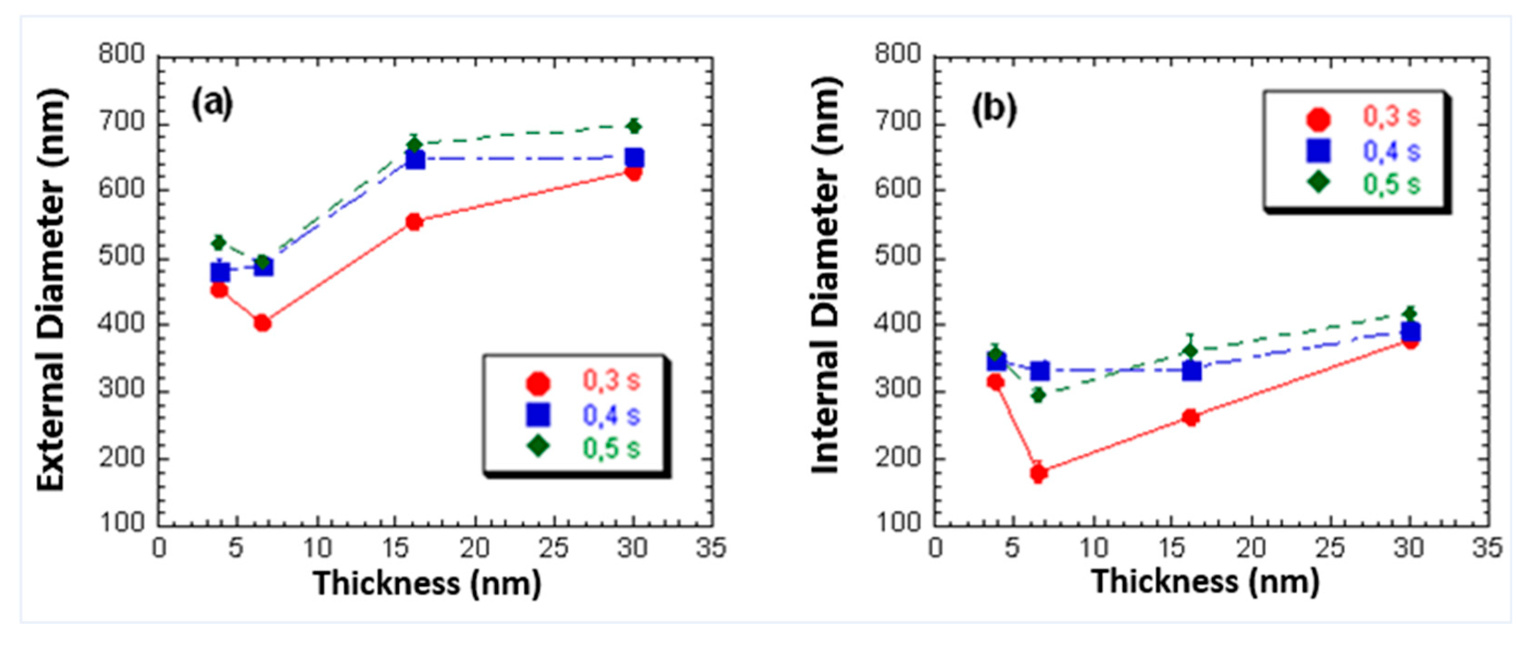
Figure 13.
Height left border (a) and height right border (b) as a function of thickness for pauses from 0.3 s to 0.5 s.
Figure 13.
Height left border (a) and height right border (b) as a function of thickness for pauses from 0.3 s to 0.5 s.
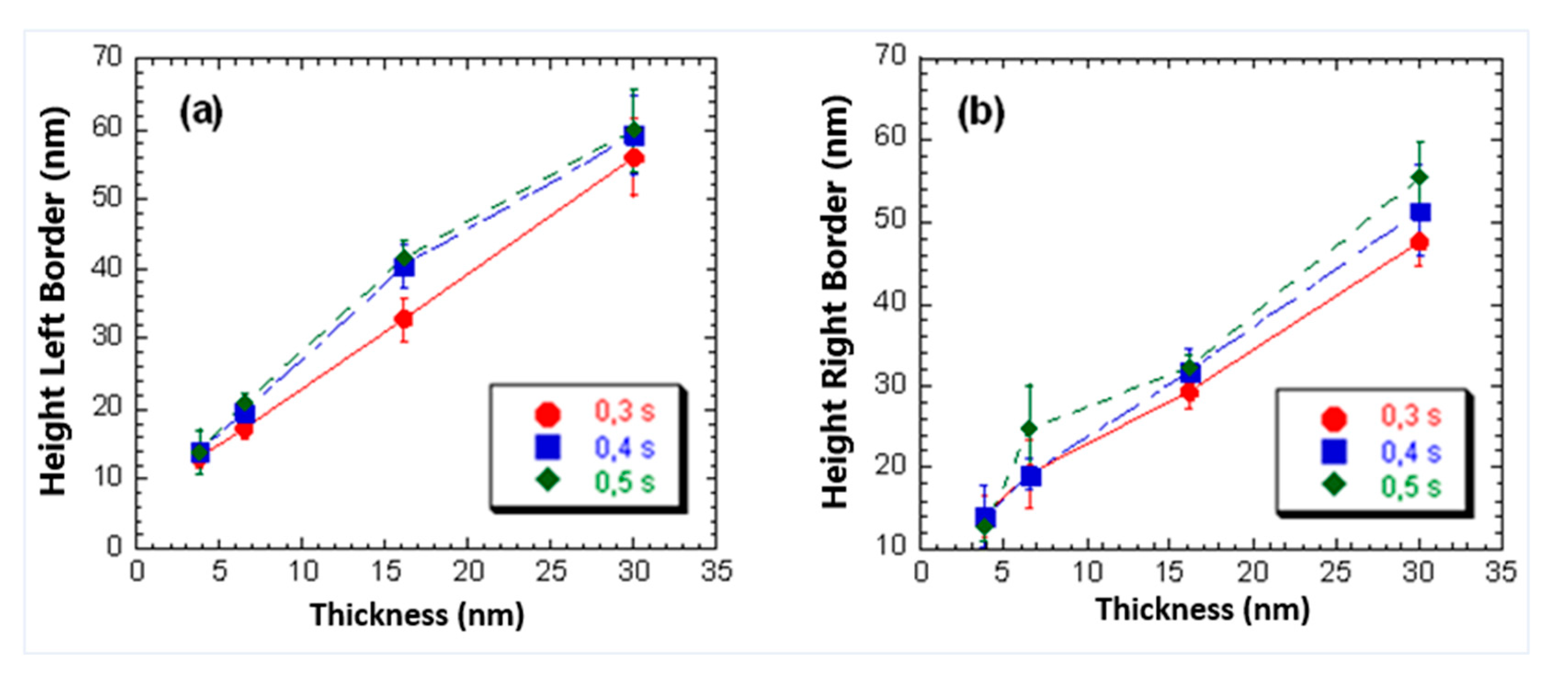
Figure 14.
Depth of holes as a function of film thickness for pauses from 0.3 s to 0.5 s.
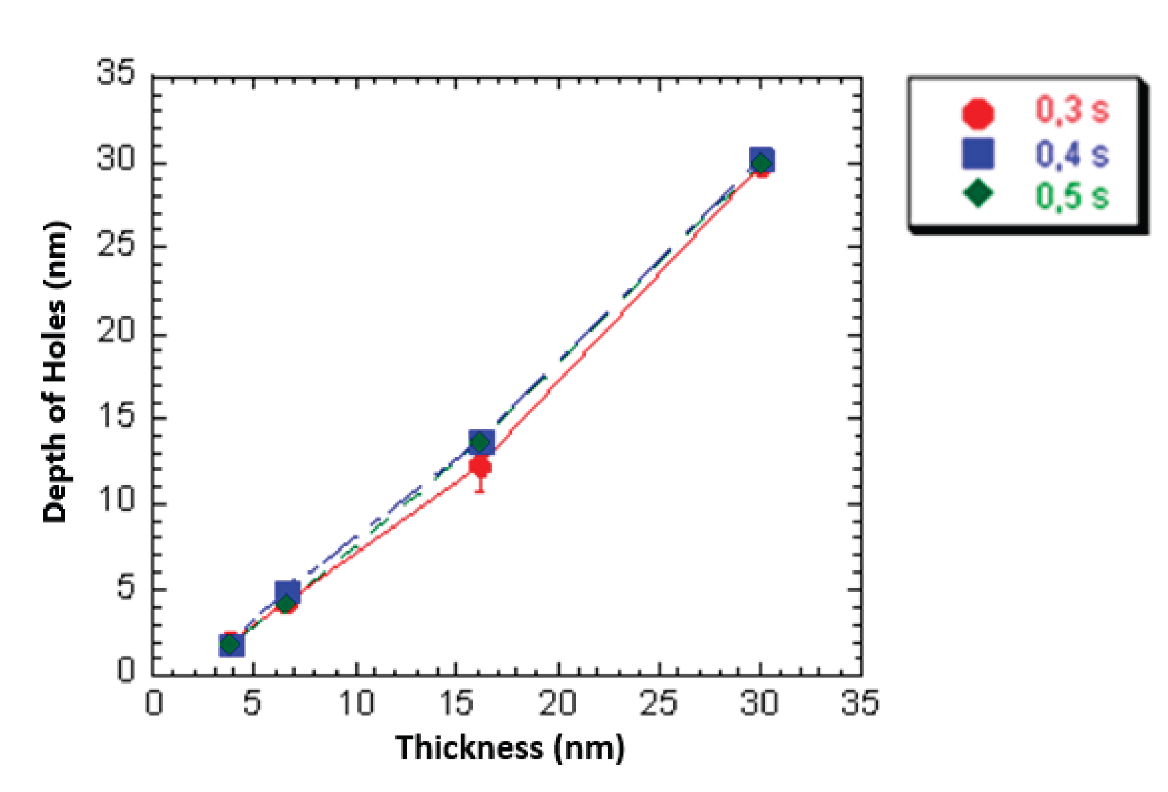

Table 1.
Values of the concentrations of solutions, resulting thicknesses and respective standard deviations.
Table 1.
Values of the concentrations of solutions, resulting thicknesses and respective standard deviations.
| Concentratiom (g/L) | Thickness (nm) | Standard Deviation (nm) |
|---|---|---|
| 1 | 3,8 | 0,8 |
| 3 | 6,5 | 0,5 |
| 5 | 16 | 0,9 |
| 15 | 30 | 2,9 |
Disclaimer/Publisher’s Note: The statements, opinions and data contained in all publications are solely those of the individual author(s) and contributor(s) and not of MDPI and/or the editor(s). MDPI and/or the editor(s) disclaim responsibility for any injury to people or property resulting from any ideas, methods, instructions or products referred to in the content. |
© 2025 by the authors. Licensee MDPI, Basel, Switzerland. This article is an open access article distributed under the terms and conditions of the Creative Commons Attribution (CC BY) license (http://creativecommons.org/licenses/by/4.0/).
Copyright: This open access article is published under a Creative Commons CC BY 4.0 license, which permit the free download, distribution, and reuse, provided that the author and preprint are cited in any reuse.


