
Submitted:
25 June 2025
Posted:
26 June 2025
You are already at the latest version
Abstract
In this study, density functional theory (DFT) and time-dependent DFT (TD-DFT) methods were employed to investigate the geometrical, electronic, optical, and photovoltaic properties of graphene (G), silicon carbide (SiC), and graphene/hexagonal boron nitride (G/h-BN) nanostructures. Dimethyl sulfoxide (DMSO) was used as a solvent to enhance the electronic behavior of the systems. Key photovoltaic parameters such as open-circuit voltage (VOC), light harvesting efficiency (LHE), and the free energies of electron injection and regeneration were evaluated. Results revealed efficient electron injection from G, SiC, and G/h-BN into the conduction band of TiO₂. The HOMO levels of G and SiC were found above the I⁻/I₃⁻ redox potential, indicating potential limitations in electron regeneration; however, this was mitigated upon dissolution in DMSO. Additionally, DMSO improved optical absorption by red-shifting the UV–visible spectra. Overall, isolated G/h-BN and the DMSO-dissolved nanostructures show promise as sensitizers in dye-sensitized solar cells (DSSCs).
Keywords:
Graphene
; Silicon-Carbide
; Graphene/Boron-Nitride
; DFT
; DSSCs
1. Introduction
In the present decade, renewable energy sources, such as wind energy, water energy, also solar energy[1], have been a focus for many researchers. One of most important sources of renewable solar energy is energy, a potential fuels alternative; photonic solar cells convert photons into electric energy [2,3]. Four kinds classify the 3rd generation of solar cells. Scientists do use nanocrystals and polymers and dyes and concentrated solar cells so as to produce these cells [4,5,6]. Dye-sensitized solar cells (DSSCs) are considered to be among the most promising solar cell fuels for the reason that they are low in price and are simple to prepare plus are nontoxic so they use natural organic material as dye sensitizers[7,8,9].
Giem as well as Novoselov's (2004) graphene discovery opened new directions for the purpose of modern sciences like that of the DSSC field. Graphene nanostructures have been used within organic solar cells as sensitizers[10,11,12,13]. This is in the field of DSSC applications. Graphene nanostructures may be considered as the first two-dimensional materials. For example, a honeycomb lattice is thought to be the most familiar shape for the graphene lattice[14,15,16,17] since carbon atoms are arranged periodically. Graphene materials have novel characteristics, such as electrons moving with high mobility and electricity conducting excellently and hardness and high flexibility; graphene, in addition, has another amazing property which is zero band gap energy[18,19,20]. At the Dirac point[21], graphene's valence bands and graphene's conduction bands intersect because of graphene's zero-bandgap property. Researchers have studied silicon carbide (SiC), boron nitride (BN), aluminum nitride (AlN), zinc oxide (ZnO), cadmium selenium (CdSe) as well as cadmium tellurium (CdTe) widely [22,23,24]. These are the materials that are considered to be two-dimensional materials similar to graphene.
Half of graphene carbon (C) atoms have been substituted with silicon (Si) atoms[25] thus forming silicon-carbide (SiC) nanoribbons. SiC nanoribbons are strong and hard with low density too. They show good electrical resistance and oxidize at good rates [26,27]. Gas sensors with hydrogen storage, catalysis, drug delivery[28,29,30] including high-frequency and high-temperature environments are potential applications of SiC nanoribbons.
Boron-nitride (BN) nanoribbons possess high oxidation rate, perfect thermal conductivity, little toxicity, and a wide energy gap (Eg~6.2 eV) [31,32,33]. Boron (B) and nitrogen (N) atoms are arranged in the honeycomb lattice like the graphene structure. Since each boron atom connects with three neighboring nitrogen atoms, three sigma bonds form within the (BN) hexagonal lattice[34,35,36]. Due to their biocompatibility, BN nanoribbons are useful in therapeutic applications[34]. In some ways, BN nanoribbons are similar to graphene. However, they have high thermal with chemical stability. Light-emitting diodes (LEDs)[37] exemplify photonic field's wide applications of BN nanoribbons. In addition, according to the more in-depth investigations of BN nanostructures, researchers have now deduced that BN emits light at a wavelength range of 200-225 nm[38,39,40].
This study was intended for the development of a more efficient light harvesting device that is for dye-sensitized solar cells (DSSCs) because of its use of graphene, silicon carbide and graphene/boron nitride nanoribbons as its sensitizers.
In 2017, Al-Rikabi conducted a study in order to examine graphene nanoflakes with the introduced thiadiazol monomer's impact. He analyzed the suggested structures' structural, electronic, and photovoltaic properties using density functional theory. Additionally, he chose the B3LYP functional along with 6-31G* energy level in order to characterize how the electrons and nuclei exchange correlation. The DFT calculations did reveal a downward shift within the energy levels of the molecular orbitals and this resulted in a reduction within the energy gap from 3.81 eV to 2.1 eV. Graphene nanoflakes with thiadiazol cause the LHE to decrease to 0.01%. Approximately 0.29% is the highest LHE value. This is found if two chains of thiadiazol are attached to the graphene nanoflake [41].
Sharma and Jha (2019) did research to study effects from boron, nitrogen, and phosphorus atoms. The study focused upon the functionalization of the carboxyl edge of graphene nanoflakes (COOH-GNFs). The structural, electrical, and optical traits of (COOH-GNF) were investigated in pure and doped forms. Relevant findings were extracted via the Gaussian 09 program. Additionally, the researchers applied the B3LYP hybrid function as well as the 6-31G* basis set. Optical calculations revealed pure COOH-GNF absorbed within the visible region, and harvested light with an efficiency of approximately 0.83%. Impacts that are meaningful on the LHE values came from elements like B, N, and P. Harvesting efficiency went down up to 0.16% when COOH-GNF was doped with boron atoms, the results indicated [42].
Kumar et al. explored the effects of adding nitrogen impurities to a graphene/flavanol nanostructure within their 2023 study also assessing its use as a DSSC sensitizer device. Electronic as well as photovoltaic properties for suggested nanocomposites were determined through use of the DFT approach. Furthermore, researchers did employ the 6-31G* energy level plus M06-2X hybrid function for them to associate highly and accurately. The data was extracted by way of their use of the GAMESS program. N impurities exist inside the graphene/flavanol nanostructure, so they greatly impact the energy gap property. Their presence causes a shift with respect to its value. As an example, band gap energy shifted with one N atom added. Energy decreased from 2.93 to 1.60. Introducing of 2 N atoms to the graphene/flavanol nanostructure resulted in an increase of the energy gap. According to the LHE results, the graphene/flavanol complex showed a far higher efficiency than other structures. An LHE of around about 0.96% was what was observed. Graphene/flavanol to which 1 N and 2 N were added had a reduced LHE. The LHE was decreased down to 0.86% and also 0.79%, respectively [43].
2. Methodology and Theoretical Approach
In the present study, the structural, electronic, optical as well as photovoltaic characteristics of graphene (G), silicon carbide (SiC), coupled with graphene/boron-nitride (G/h-BN) nanoribbons, will be investigated via density functional theory (DFT) also time-dependent (TD-DFT) methods, with the effect of the DMSO solvent on such properties to be studied furthermore. DFT calculates ground state properties so TD-DFT computes excitation state characteristics. For relaxation calculation, we consider the bond lengths, bond angles, and binding energies. We include the molecular orbital energy, energy gap, and density of states (DOS) spectrum to describe electronic properties. Oscillation strength, such as f, along with the maximum wavelength regarding absorption, for instance λMax, involve excitation state properties. For the photovoltaic parameters, open-voltaic circuits, light harvesting efficiency, and free energy for electron injection and regeneration are demanded.
The efficiency of power conversion (η) is defined as the ratio of solar energy converted by a solar cell into usable electrical energy, calculated using the following equation [44]:
where () is the incident power density, () is the open-circuit voltage, ( ) is the short-circuit current density, and (FF) is the fill factor.
The open-circuit voltage () plays a critical role in electron injection from the Lowest Unoccupied Molecular Orbital (LUMO) into the conduction band minimum (of semiconductor materials, such as titanium dioxide (TiO₂) or zinc oxide (ZnO) [45]. The relationship between () and the LUMO energy level is given by:
The short-circuit current density ( ) in a dye-sensitized solar cell (DSSC) can be determined by:
Where (), () and () represent the light harvesting efficiency, electron injection efficiency, and charge collection efficiency, respectively. The LHE parameter is evaluated by the following equation [47,48]:
Where is the oscillator strength at the maximum absorption wavelength.
The free energy of electron injection ) describes the energy required to inject electrons from the excited state of the DSSC sensitizer into the conduction band of semiconductor materials, given by [49,50]:
Where ) is the excited-state oxidation potential of the nanostructure, and X denotes the selected two-dimensional nanostructure.
The excited-state oxidation potential ) can be obtained from the oxidation potential ) and excitation energy of the nanostructures using [51]:
Finally, the free energy of electron regeneration indicates the energy difference between the oxidation potential of the nanostructure and the redox potential of the iodine/triiodide electrolyte, typically -4.85 eV for (), and is calculated as [52]:
3. Results and Discussions
3.1. Geometrical Relaxation
In this section, we investigate the geometrical properties, including bond lengths and bond angles, of the relaxed graphene (G), silicon carbide (SiC), and graphene/boron nitride (G/h-BN) nanostructures. Figure 1 illustrates the geometrically relaxed structures of these nanomaterials.
DFT calculations revealed that the G nanostructures have 4 types of bonds between atoms: C-C, C=C, C…C and C-H. Similarly, calculations have shown that, for BN nanostructures, there are three types of bonds between boron (B), nitrogen (N) and hydrogen (H) B-N, B-H and N-H. Moreover, SiC nanostructures have four types of bonds between silicon (Si), carbon (C) and H atoms Si-C, Si…C, Si-H, C-H. The relaxation calculations revealed that the G, SiC and BN surfaces had planar shapes [53,54,55].
Angle length calculations revealed that there are many types of angles between atoms in the G, SiC and BN nanostructures; thus, only primary atoms such as B and N in BN were considered for the G and SiC systems [56,57,58]. Table (1) shows the calculations of the bond lengths and angle lengths between atoms in the G, SiC and BN nanostructures.

Table 1.
Indexed bond lengths and angle lengths between atoms in the G, SiC and G/h-BN nanostructures computed by the DFT method measured in Angstrom unit.
Table 1.
Indexed bond lengths and angle lengths between atoms in the G, SiC and G/h-BN nanostructures computed by the DFT method measured in Angstrom unit.
|
|
|
|
|
|
| G |
|
|
|
|
|
|
|
|
|
|
|
|
|
|
|
|
|
|
|
|
|
|
| SiC |
|
|
|
|
|
|
|
|
|
|
|
|
|
|
|
|
|
|
|
|
|
|
| G/h − BN |
|
1.40-1.43 |
|
119.47-122.17 |
|
|
1.42-1.43 |
|
119.13-121.61 | |
|
|
1.52-1.53 |
|
118.81-120.01 | |
|
|
1.43-1.47 |
|
119.71-120.08 | |
|
|
118.50- 119.06 | |||
|
|
118.21-120.23 | |||
3.2. Electronic Properties
In this section, Density Functional Theory (DFT) is employed to calculate the molecular orbital energies (HOMO and LUMO) and energy gaps (Eg) of graphene (G), silicon carbide (SiC), and graphene/boron nitride (G/h-BN) nanostructures, in both isolated and dissolved phases. The DFT calculations ensure the nanostructures meet the electron injection and regeneration requirements essential for photovoltaic applications.
Table 2A summarizes the molecular orbital energies and corresponding band gaps for the isolated nanostructures. The results indicate similar HOMO energy levels for G and SiC, attributable to the comparable electronic configurations of carbon and silicon atoms, both situated in group IV of the periodic table. In contrast, the HOMO energy level of the G/h-BN nanostructure is significantly lower compared to G and SiC [59,60]. Band gap energy analysis reveals that G/h-BN possesses the widest band gap (3.460 eV), whereas G and SiC have narrower band gaps, approximately 2.287 eV and 2.134 eV, respectively [61]. This implies higher electrical conductivities for G and SiC compared to the G/h-BN nanostructure, due to their narrower molecular orbital energies.
Table 2B displays the calculated molecular orbital energies and energy gaps for G, SiC, and G/h-BN nanostructures dissolved in dimethyl sulfoxide (DMSO). The solvent significantly influences the orbital energies of G and SiC due to their organic characteristics. For example, the HOMO energy of SiC shifts from -4.666 eV (isolated state) to -4.927 eV upon dissolution. Consequently, the band gap energy also increases from 2.134 eV (isolated) to 2.684 eV (dissolved). However, the metallic-like structure of BN limits notable changes in molecular orbital and band gap energies when dissolved, reflected in minor shifts (HOMO shifts from -5.019 eV to -5.251 eV).
Table 2B.
Indexed molecular orbital energy (EHOMO and ELUMO) and energy gap (Eg) in dissolved phase measured in eV.
Table 2B.
Indexed molecular orbital energy (EHOMO and ELUMO) and energy gap (Eg) in dissolved phase measured in eV.
|
|
|
|
|
|
|
|
|
|
|
|
|
|
|
|
|
|
|
|
Figure 2A illustrates the Density of States (DOS) spectra for the studied nanostructures in isolated and dissolved states. The analysis shows that dissolution in DMSO generally results in HOMO energy level shifts toward lower energies. Specifically, the HOMO energy for graphene shifts from -4.675 eV to -4.853 eV. While LUMO levels of G and G/h-BN nanostructures also shift toward lower energies, the SiC nanostructure displays a slight increase in its LUMO energy level. Consequently, the band gap of SiC notably widens from 2.134 eV to 2.684 eV upon dissolution.
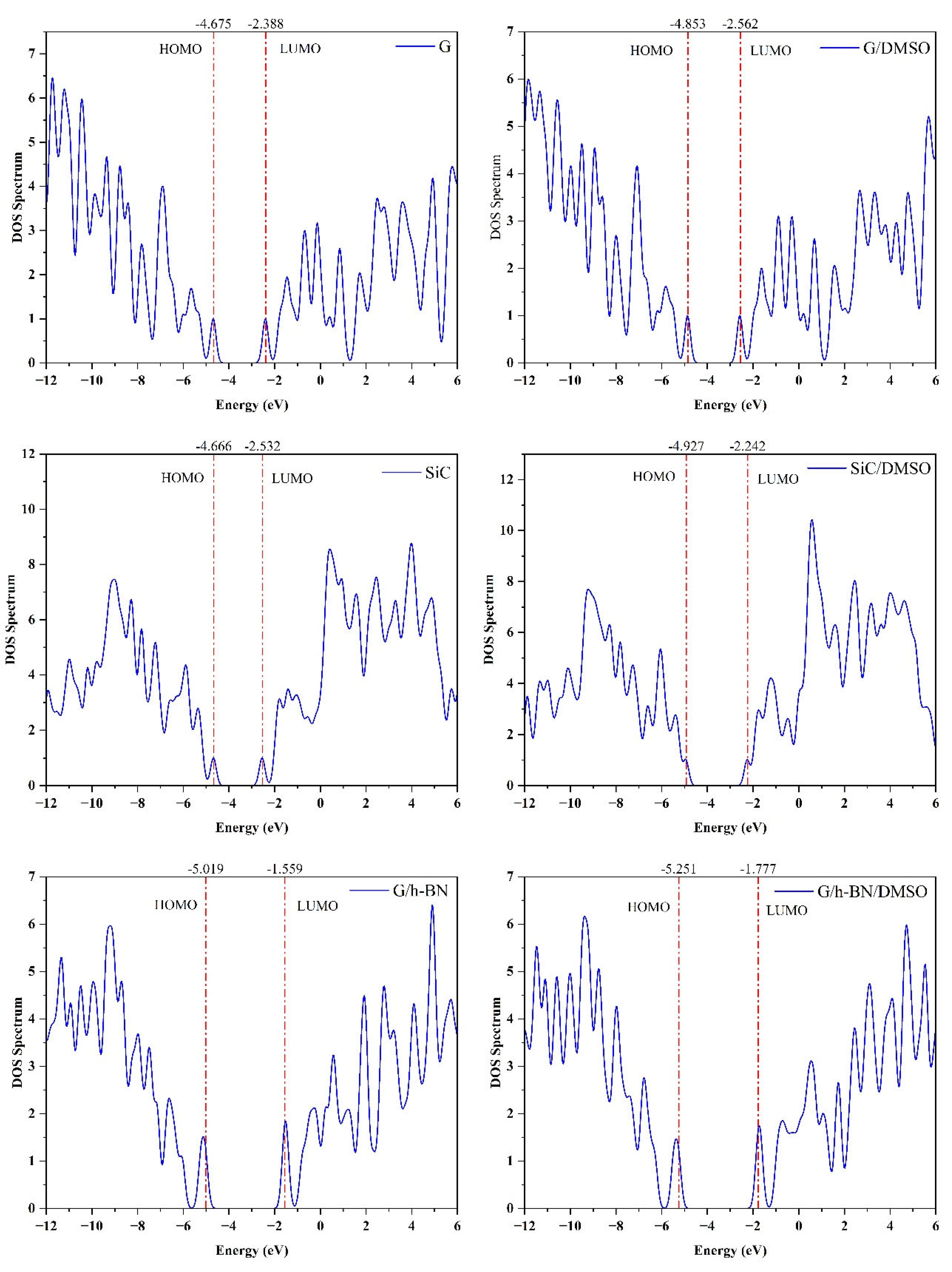
Figure 2A.
Density of state spectra and charge density distributions for the G, SiC and G/h-BN nanostructures in the isolated and dissolved phases.
Figure 2A.
Density of state spectra and charge density distributions for the G, SiC and G/h-BN nanostructures in the isolated and dissolved phases.
Charge density distribution calculations reveal that, in graphene, the highest density is symmetrically distributed around carbon atoms for both HOMO and LUMO orbitals. For SiC and BN nanostructures, the charge density is predominantly localized around edge atoms, especially in the LUMO orbitals. Additionally, the HOMO orbitals in SiC and G/h-BN nanostructures exhibit high charge density primarily surrounding the carbon atoms. Importantly, the presence of the DMSO solvent does not significantly affect the charge density distribution within these nanostructures. Figure 2B visually presents the charge density distribution patterns for isolated and dissolved G, SiC, and G/h-BN nanostructures.
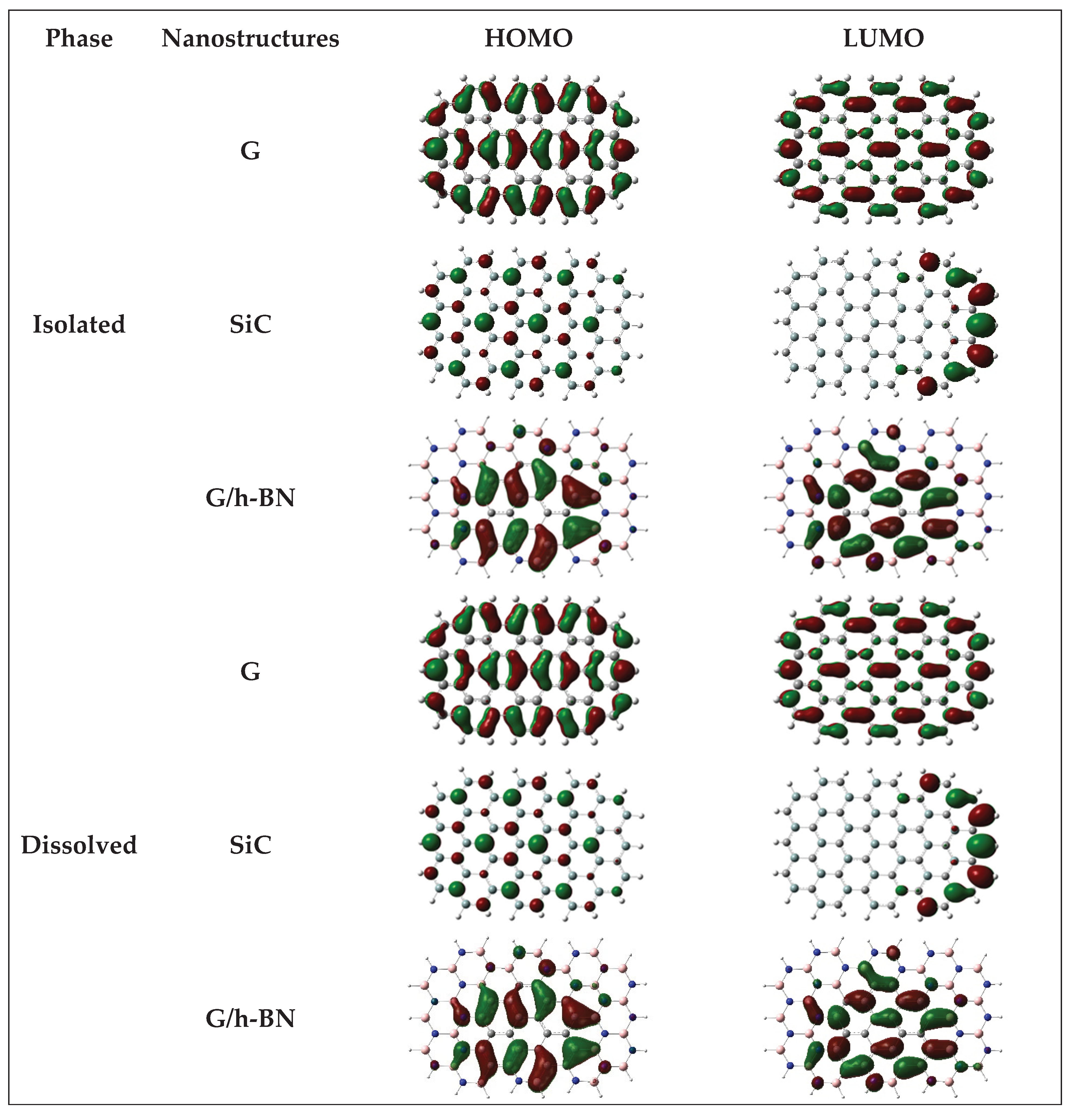
Figure 2B.
showed the charge density distributions for isolated and dissolved G, SiC and G/h-BN nanostructures.
Figure 2B.
showed the charge density distributions for isolated and dissolved G, SiC and G/h-BN nanostructures.
One of the crucial factors for assessing dye-sensitized solar cell (DSSC) sensitizer performance is the molecular orbital distribution relative to the conduction band minimum () of the titanium dioxide semiconductor and the iodine/triiodide electrolyte () [62,63]. For an efficient electron-transfer cycle, the following criteria must be met:
A- The energy level must lie below the redox potential of the electrolyte.
B- The energy level must be positioned above the of the semiconductor.
In the isolated phase, density functional theory (DFT) calculations revealed that all LUMO levels are positioned above the , indicating effective electron injection capabilities for all nanostructures studied. However, the HOMO levels of graphene (G) and silicon carbide (SiC) nanostructures are positioned above the electrolyte redox potential, indicating these structures lack the ability to regenerate electrons in their ground states. In contrast, the G/h-BN nanostructure's HOMO level is situated below the electrolyte redox potential, allowing efficient electron regeneration in the ground state. Figure 3 illustrates the molecular orbital energies of G, SiC, and G/h-BN nanostructures in relation to the and .electrolyte in the isolated state.
Chemical solvents often enhance electronic properties of nanostructures through molecular interactions [64]. Here, dimethyl sulfoxide (DMSO) was selected as a solvent to enhance the electronic properties of the G, SiC, and G/h-BN nanostructures.
Upon dissolution, DFT calculations showed that the HOMO levels of G and SiC shifted downward, moving below the electrolyte’s redox potential due to interactions between nanostructure electrons and DMSO molecules. This shift enables electron regeneration in the ground states of G and SiC nanostructures. Additionally, dissolution in DMSO enhances electron injection capability into due to increased interaction between electrons and the solvent. Figure 4 illustrates these improvements, demonstrating that dissolved G, SiC, and G/h-BN meet the criteria for both electron injection and regeneration.
3.3. Photovoltaic Parameters
An ideal electron injection-regeneration cycle within DSSCs involves electron transfer from the LUMO of the sensitizer into the , followed by electron regeneration at the HOMO level. Photovoltaic performance is evaluated by parameters such as the free energy of electron injection ), free energy of electron regeneration ), open-circuit voltage (Voc), and light harvesting efficiency (LHE) [65]. Table 3 summarizes these parameters for the nanostructures studied in both isolated and dissolved phases.
For the isolated phase, calculations revealed negative values for the free energy of electron injection ), indicating that the excited-state energies of all studied nanostructures (graphene (G), silicon carbide (SiC), and graphene/boron nitride (G/h-BN)) lie above the conduction band minimum (CBM) of the titanium dioxide semiconductor. This confirms their effective capability for electron injection into the semiconductor. Similarly, in the dissolved state (with DMSO solvent), the free energy of electron injection remained negative for all nanostructures, confirming the sustained capability for electron injection. Moreover, the magnitude of the electron injection energy increased for G and SiC upon dissolution in DMSO, whereas it slightly decreased for G/h-BN.
Regarding electron regeneration, the calculations indicated that isolated G and SiC nanostructures exhibit positive values of free energy for electron regeneration (), suggesting their inability to regenerate electrons because their HOMO energy levels lie above the electrolyte redox potential. Conversely, the isolated G/h-BN nanostructure exhibited a negative (), demonstrating effective electron regeneration capability due to its HOMO energy level lying below the redox potential.
The use of DMSO solvent notably improved electron regeneration properties. Dissolving the G and SiC nanostructures in DMSO caused their (), values to shift from positive to negative. This shift confirms that interactions between electrons in the nanostructures and DMSO solvent molecules lowered the HOMO energy levels below the electrolyte redox potential, thus enabling efficient electron regeneration. These findings indicate that electrons regenerated at the HOMO can re-inject into the CBM of , promoting a continuous electron injection-regeneration cycle. Furthermore, larger negative values of electron injection energy ) and smaller negative values of electron regeneration energy (), indicate faster and more efficient charge transfer processes between the nanostructures and electrolyte. Importantly, the G/h-BN nanostructure exhibited favorable electron injection and regeneration characteristics in both isolated and dissolved states.
Another critical parameter that reflects electron injection capability into the CBM of is the open-circuit voltage (Voc). According to Equation (2), (Voc) is directly proportional to the lower unoccupied molecular orbital (LUMO) energy. The calculated results in Table 3 demonstrate that both isolated and dissolved nanostructures exhibit high electron injection capabilities from their LUMO levels into the semiconductor. Notably, SiC nanostructures demonstrated a significant increase in electron injection capability upon dissolution in DMSO, reflected in the enhanced (Voc) values. Overall, both isolated and dissolved forms of the studied nanostructures are capable of efficiently injecting electrons into the CBM due to their appropriately positioned LUMO levels. Figure 5 provides a clear comparison of the computed (Voc) values for the isolated and dissolved nanostructures, measured in volts (V).
3.4. UV-Visible Spectrum and LHE Properties
In this section, the maximum absorption wavelength (λmax), oscillation strength , and light harvesting efficiency (LHE) of graphene (G), silicon carbide (SiC), and graphene/boron nitride (G/h-BN) nanostructures are investigated using time-dependent density functional theory (TD-DFT). Calculations were conducted employing the B3LYP hybrid functional and the 6-31G* basis set to accurately describe electron exchange-correlation processes. Figure 6 illustrates the UV–visible absorption spectra for isolated and dissolved (in DMSO solvent) nanostructures, considering twenty electronic transitions
For isolated G, TD-DFT results revealed two significant absorption peaks: the first at approximately 391.42 nm and the second at approximately 584.15 nm [66]. Major electronic transitions were identified as and . This study specifically highlights the 584.15 nm peak due to its strong absorption within the visible spectrum and higher oscillation strength. In the isolated SiC nanostructure, a single absorption peak was located at approximately 481.82 nm, primarily characterized by the transition (96%) [67], exhibiting an oscillation strength of approximately 0.20. Similarly, the isolated G/h-BN displayed a notable absorption band at approximately 361.16 nm, characterized by the transition (67%) [68], with a relatively high oscillation strength of approximately 0.871.
Upon dissolution in DMSO, TD-DFT analysis indicated distinct shifts in maximum absorption wavelengths and improvements in oscillation strengths. For the G nanostructure, absorption shifted from 584.15 nm (isolated) to 600.07 nm (dissolved), indicating a redshift due to electron interactions between the G nanostructure and DMSO solvent. Correspondingly, the oscillation strength increased significantly, from 0.723 to 1.109. For the SiC nanostructure, dissolution caused a blueshift from 481.82 nm to 443.21 nm; notably, its oscillation strength improved to approximately 0.51, reflecting enhanced light harvesting capability due to solvent interactions.
In contrast, the G/h-BN nanostructure exhibited minimal spectral changes upon dissolution, with the maximum absorption wavelength shifting slightly from 361.16 nm to 361.06 nm (approximately 0.1 nm shift). This negligible shift reflects the metallic-like characteristics of BN, leading to weaker interactions with the solvent. Nevertheless, the oscillation strength notably improved from 0.871 to 1.366, indicating a significant enhancement in its ability to absorb incident light.
Besides electron injection energy , electron regeneration energy , and open-circuit voltage (, the light harvesting efficiency (LHE) is another crucial parameter for evaluating DSSC performance. LHE quantifies the effectiveness of incident photon absorption by nanostructures. Figure 7 illustrates the calculated LHE values for the studied nanostructures. According to Equation (4), the LHE value increases with greater oscillation strength. In isolated conditions, the G nanostructure demonstrated superior LHE (~84.93%) compared to SiC and G/h-BN, indicating its higher efficiency in harvesting incident photons. However, despite their significant absorption capabilities, isolated G and SiC could not regenerate electrons effectively due to their HOMO energy levels.
In the dissolved phase, calculations indicated significant improvement in the light harvesting efficiency (LHE), particularly for the SiC nanostructure when dissolved in DMSO. Specifically, the harvesting efficiency increased dramatically from 35.73% (isolated) to 69.09% (dissolved). Moreover, the G and G/h-BN nanostructures demonstrated notably high efficiencies in absorbing incident light upon dissolution. Collectively, these results confirm that utilizing DMSO as a solvent markedly enhances the ability of these nanostructures to harvest incident light, subsequently improving their potential for converting solar energy into electrical energy.
4. Conclusions
Density functional theory (DFT) and time-dependent density functional theory (TD-DFT) methods were employed to comprehensively analyze structural, electronic, optical, and photovoltaic properties of isolated and dissolved graphene (G), silicon carbide (SiC), and graphene/boron nitride (G/h-BN) nanostructures. Geometrical relaxation analyses revealed no significant structural changes due to dissolution in dimethyl sulfoxide (DMSO). However, electronic property analyses showed notable decreases in molecular orbital energies upon dissolution, resulting in wider energy gaps compared to isolated phases, especially prominent in the SiC nanostructure.
The calculations for electron injection and electron regeneration energies confirmed that the studied nanostructures possess suitable oxidation and reduction potentials. Moreover, photovoltaic parameter assessments demonstrated substantial enhancements when these nanostructures were dissolved in DMSO, reflecting improved photovoltaic performance over isolated conditions. Overall, these findings indicate that the studied nanostructures, especially when dissolved in DMSO, exhibit strong potential as sensitizers in dye-sensitized solar cells (DSSCs).
Author Contributions
For research articles with several authors, a short paragraph specifying their individual contributions must be provided. The following statements should be used “Conceptualization, Mohammed A. Al-Seady. and Hayder M. Abduljalil.; methodology, Ruqayah Ali Grmasha, 5 and Hussein Hakim Abed.; software, X.X.; validation, Noor Al-Huda Saleh, Mezna Al-Rashdi,. and Mohammed A. Al-Seady.; formal analysis, Eman Hamid Hussein.; original draft preparation, Hayder M. Abduljalil; writing—review and editing, Mohammed A. Al-Seady and Hussein Hakim Abed.; supervision, Hayder M. Abduljalil and Mohammed A. Al-Seady; All authors have read and agreed to the published version of the manuscript.” Please turn to the CRediT taxonomy for the term explanation. Authorship must be limited to those who have contributed substantially to the work reported.
Funding
This research received no external funding.
Data Availability Statement
We encourage all authors of articles published in MDPI journals to share their research data. In this section, please provide details regarding where data supporting reported results can be found, including links to publicly archived datasets analyzed or generated during the study. Where no new data were created, or where data is unavailable due to privacy or ethical restrictions, a statement is still required. Suggested Data Availability Statements are available in section “MDPI Research Data Policies” at https://www.mdpi.com/ethics.
Acknowledgments
There is no acknowledgment.
Conflicts of Interest
The authors have no relevant financial or nonfinancial interests to disclose.
References
- Jurasz, J. , Canales, F., Kies, A., Guezgouz, M., Beluco, A. A (2020) review on the complementarity of renewable energy sources: Concept, metrics, application and future research directions. Solar Energy. 195, 703-24. [CrossRef]
- Al-Seady, M.A. , Abed, H.H., Alghazaly, S.M., Salman, J.M., Abduljalil, H.M., Altemimei, F.A., Hashim, A., Abdulsattar, M.A., Allan, L., Kahaly, M.U. (2023) Prospective utilization of boron nitride and beryllium oxide nanotubes for Na, Li, and K-ion batteries: a DFT-based analysis. Journal of Molecular Modeling. 29, 1-20. [CrossRef]
- Zheng, X. , Zhang, L. (2016) Photonic nanostructures for solar energy conversion. Energy & Environmental Science. 9, 2511-32. [CrossRef]
- Akinoglu, B.G. , Tuncel, B. , Badescu, V. (2021) Beyond 3rd generation solar cells and the full spectrum project. Recent advances and new emerging solar cells. Sustainable Energy Technologies and Assessments. 46, 101287. [CrossRef]
- Babar, F. , Mehmood, U., Asghar, H., Mehdi, M.H., Khan, A.U.H., Khalid, H., ul Huda, N., Fatima, Z. (2020) Nanostructured photoanode materials and their deposition methods for efficient and economical third generation dye-sensitized solar cells: A comprehensive review. Renewable and Sustainable Energy Reviews. 129, 109919. [CrossRef]
- Maçaira, J. , Andrade, L., Mendes, A. (2013) Review on nanostructured photoelectrodes for next generation dye-sensitized solar cells. Renewable and Sustainable Energy Reviews. 27, 334-49. [CrossRef]
- Kabir, F. , Manir, S., Bhuiyan, M.M.H., Aftab, S., Ghanbari, H., Hasani, A., Fawzy, M., De Silva, G.T., Mohammadzadeh, M.R., Ahmadi, R. (2022) Instability of dye-sensitized solar cells using natural dyes and approaches to improving stability–an overview. Sustainable Energy Technologies and Assessments. 52, 102196. [CrossRef]
- Kaliramna, S. , Dhayal, S.S., Chaudhary, R., Khaturia, S., Ameta, K.L., Kumar, N. (2022) A review and comparative analysis of different types of dyes for applications in dye-sensitized solar cells. Brazilian Journal of Physics. 52, 136. [CrossRef]
- Semalti, P. , Sharma, S.N. (2020) Dye sensitized solar cells (DSSCs) electrolytes and natural photosensitizers: a review. Journal of nanoscience and nanotechnology. 20, 3647-58. [CrossRef]
- Badhulika, S. , Terse-Thakoor, T., Villarreal, C., Mulchandani, A. (2015) Graphene hybrids: synthesis strategies and applications in sensors and sensitized solar cells. Frontiers in chemistry. 3, 38. [CrossRef]
- Kahaly, M.U. , Schwingenschlögl, U. (2014) Enhanced solar light absorption of graphene by interaction with anisole. Carbon. 77, 76-9. [CrossRef]
- Oni, A.M. , Mohsin, A.S. , Rahman, M.M. , Bhuian, M.B.H. (2024) A comprehensive evaluation of solar cell technologies, associated loss mechanisms, and efficiency enhancement strategies for photovoltaic cells. Energy Reports. 11, 3345-66. [CrossRef]
- Wolf, E.L. 2014 Applications of graphene: an overview, Springer. [CrossRef]
- Armano, A. , Agnello, S. (2019) Two-dimensional carbon: a review of synthesis methods, and electronic, optical, and vibrational properties of single-layer graphene. C., 5, 67. [CrossRef]
- Jana, S. , Bandyopadhyay, A., Datta, S., Bhattacharya, D., Jana, D. (2021) Emerging properties of carbon based 2D material beyond graphene. Journal of Physics: Condensed Matter. 34, 053001. [CrossRef]
- Kahaly, M.U. , Waghmare, U.V. (2007) Vibrational properties of single-wall carbon nanotubes: A first-principles study. Journal of Nanoscience and Nanotechnology. 7, 1787-92. [CrossRef]
- Xu, M. , Liang, T., Shi, M., Chen, H. (2013) Graphene-like two-dimensional materials. Chemical reviews. 113, 3766-98. [CrossRef]
- Huang, X. , Yin, Z., Wu, S., Qi, X., He, Q., Zhang, Q., Yan, Q., Boey, F., Zhang, H. (2011) Graphene-based materials: synthesis, characterization, properties, and applications. small. 7, 1876-902. [CrossRef]
- Soldano, C. , Mahmood, A. , Dujardin, E. (2010) Production, properties and potential of graphene. Carbon. 48, 2127-50. [CrossRef]
- Sun, Y. , Sun, M., Xie, D. (2018) Graphene electronic devices. In: Graphene, Elsevier, pp. 103-55. [CrossRef]
- Thuy Tran, N.T. , Dahal, D., Gumbs, G., Lin, M.-F. (2017) Adatom doping-enriched geometric and electronic properties of pristine graphene: a method to modify the band gap. Structural Chemistry. 28, 1311-8. [CrossRef]
- Chabi, S. , Guler, Z., Brearley, A.J., Benavidez, A.D., Luk, T.S. (2021) The creation of true two-dimensional silicon carbide. Nanomaterials. 11, 1799. [CrossRef]
- Leonardi, S.G. (2017) Two-dimensional zinc oxide nanostructures for gas sensor applications. Chemosensors. 5, 17. [CrossRef]
- Tran, T.N. , Nguyen, T.A., Anh Duy, N.V., Nguyen, T.L., Dinh, V.A., Schall, P., Dang, M.T. (2014) Adsorption of cadmium selenide clusters: A novel approach to enhance solar energy conversion using armchair graphene nanoribbons. AIP Advances. 14. [CrossRef]
- Taheri, N. , Moradi, M., Farzad, M.H. (2022) Structural, electronic and magnetic properties of some adatoms adsorbed at the edges and Mg-doped SiC nanoribbons. Computational Condensed Matter. 32, e00722. [CrossRef]
- Liu, H. , Zhang, X., Xu, N., Han, C., Wu, N., Wang, B., Wang, Y. (2024) Progress of One-Dimensional SiC Nanomaterials: Design, Fabrication and Sensing Applications. Nanomaterials. 14, 187. [CrossRef]
- Ojha, G.P. , Kang, G.W., Kuk, Y.-S., Hwang, Y.E., Kwon, O.H., Pant, B., Acharya, J., Park, Y.W., Park, M. (2022) Silicon Carbide nanostructures as potential carbide material for electrochemical supercapacitors: A review. Nanomaterials. 13, 150. [CrossRef]
- Johnson, A.P. , Gangadharappa, H., Pramod, K. (2020) Graphene nanoribbons: A promising nanomaterial for biomedical applications. Journal of controlled release. 325, 141-62. [CrossRef]
- Noreen, S. , Tahir, M.B., Hussain, A., Nawaz, T., Rehman, J.U., Dahshan, A., Alzaid, M., Alrobei, H. (2022) Emerging 2D-Nanostructured materials for electrochemical and sensing Application-A review. International Journal of Hydrogen Energy. 47, 1371-89. [CrossRef]
- Wu, R. , Zhou, K. , Yue, C.Y. , Wei, J. , Pan, Y. (2015) Recent progress in synthesis, properties and potential applications of SiC nanomaterials. Progress in Materials Science. 72, 1-60. [CrossRef]
- Kahaly, M.U. , Waghmare, U.V. (2008) Electronic structure of carbon doped boron nitride nanotubes: a first-principles study. Journal of Nanoscience and Nanotechnology. 8, 4041-8. [CrossRef]
- Laghaei, M. , Ghasemian, M., Lei, W., Kong, L., Chao, Q. (2023) A review of boron nitride-based photocatalysts for carbon dioxide reduction. Journal of Materials Chemistry A. 11, 11925-63. [CrossRef]
- Shtansky, D.V. , Matveev, A.T., Permyakova, E.S., Leybo, D.V., Konopatsky, A.S., Sorokin, P.B. (2022) Recent progress in fabrication and application of BN nanostructures and BN-based nanohybrids. Nanomaterials. 12, 2810. [CrossRef]
- Akman, N. , Özdoğan, C. (2018) Island shape, size and interface dependency on electronic and magnetic properties of graphene hexagonal-boron nitride (h-BN) in-plane hybrids. Journal of Physics and Chemistry of Solids. 115, 187-98. [CrossRef]
- Li, D. , Gao, J., Cheng, P., He, J., Yin, Y., Hu, Y., Chen, L., Cheng, Y., Zhao, J. (2020) 2D boron sheets: structure, growth, and electronic and thermal transport properties. Advanced Functional Materials. 30, 1904349. [CrossRef]
- Roy, S. , Zhang, X., Puthirath, A.B., Meiyazhagan, A., Bhattacharyya, S., Rahman, M.M., Babu, G., Susarla, S., Saju, S.K., Tran, M.K. (2021) Structure, properties and applications of two-dimensional hexagonal boron nitride. Advanced Materials. 33, 2101589. [CrossRef]
- Wang, H. , Wang, H.S. , Ma, C. , Chen, L. , Jiang, C. , Chen, C. , Xie, X. , Li, A.-P. , Wang, X. (2021) Graphene nanoribbons for quantum electronics. Nature Reviews Physics. 3, 791-802. [CrossRef]
- Kadhim, Q.S. , Abdoon, R.S., Mohammed, H.T., Abbas, A.S., Al-Seady, M.A., Nagy, G., Abduljalil, H.M., Saleh, N.A.-H., Kahaly, M.U. (2022) Effect of metal ad-atoms on the structural, electrical, and optical properties of boron-nitride nanostructures toward optoelectronics: a DFT based study. Egyptian Journal of Chemistry. 65, 745-52. [CrossRef]
- Raidongia, K. , Jagadeesan, D., Upadhyay-Kahaly, M., Waghmare, U., Pati, S.K., Eswaramoorthy, M., Rao, C. (2008) Synthesis, structure and properties of homogeneous BC 4 N nanotubes. Journal of Materials Chemistry. 18, 83-90. [CrossRef]
- Wang, J. , Ma, F., Liang, W., Wang, R., Sun, M. (2017) Optical, photonic and optoelectronic properties of graphene, h-BN and their hybrid materials. Nanophotonics. 6, 943-76. [CrossRef]
- Alrikabi, A. (2017) Theoretical study of the design dye-sensitivity for usage in the solar cell device. The results in physics. 7, 4359-63. [CrossRef]
- Sharma, V. , Jha, P.K. (2019) Enhancement in power conversion efficiency of edge-functionalized graphene quantum dot through adatoms for solar cell applications. Solar Energy Materials and Solar Cells. 200, 109908. [CrossRef]
- Kumar, A. , Ameer, S.A.A. , Mohealdeen, S.M. , Hasoon, A. , Abdulsayed, Y.A. , Lagum, A.A. , Al-Ma'abreh, A.M. , Kadhim, M.M. (2023) Performance enhancement of dye-sensitized solar cells based on nitrogen-doped graphene quantum dots. Computational and Theoretical Chemistry. 1226, 114180. [CrossRef]
- Janjua, M.R.S.A. , Khan, M.U., Khalid, M., Ullah, N., Kalgaonkar, R., Alnoaimi, K., Baqader, N., Jamil, S. (2021) Theoretical and conceptual framework to design efficient dye-sensitized solar cells (DSSCs): molecular engineering by DFT method. Journal of Cluster Science. 32, 243-53. [CrossRef]
- Azaid, A. , Raftani, M., Alaqarbeh, M., Kacimi, R., Abram, T., Khaddam, Y., Nebbach, D., Sbai, A., Lakhlifi, T., Bouachrine, M. (2022) New organic dye-sensitized solar cells based on the D–A–π–A structure for efficient DSSCs: DFT/TD-DFT investigations. RSC advances. 12, 30626-38. [CrossRef]
- Britel, O. , Fitri, A., Benjelloun, A.T., Slimi, A., Benzakour, M., Mcharfi, M. (2022) Theoretical design of new carbazole based organic dyes for DSSCs applications. A DFT/TD-DFT insight. Journal of Photochemistry and Photobiology A: Chemistry. 429, 113902. [CrossRef]
- El-Shishtawy, R.M. , Asiri, A.M., Aziz, S.G., Elroby, S.A. (2014) Molecular design of donor-acceptor dyes for efficient dye-sensitized solar cells I: a DFT study. Journal of molecular modeling. 20, 1-9. [CrossRef]
- Etabti, H. , Fitri, A., Benjelloun, A.T., Hachi, M., Benzakour, M., Mcharfi, M. (2021) Benzocarbazole-based D–Di–π–A dyes for DSSCs: DFT/TD-DFT study of influence of auxiliary donors on the performance of free dye and dye–TiO2 interface. Research on Chemical Intermediates. 47, 4257-80. [CrossRef]
- Abed, H.H. , Al-Aaraji, N.A.-H., Salman, J.M., Abduljalil, H.M., Al-Seady, M.A. (2022) Theoretical study on dye-sensitized solar cells using graphene quantum dot and curcumin, pahthalocyanine dyes. In: IOP Conference Series: Earth and Environmental Science, IOP Publishing, Vol. 1088, p. 012012. [CrossRef]
- Xu, Z. , Li, Y., Zhang, W., Yuan, S., Hao, L., Xu, T., Lu, X. (2019) DFT/TD-DFT study of novel T shaped phenothiazine-based organic dyes for dye-sensitized solar cells applications. Spectrochimica Acta Part A: Molecular and Biomolecular Spectroscopy. 212, 272-80. [CrossRef]
- Mendizabal, F. , Lopéz, A., Arratia-Pérez, R., Zapata-Torres, G. (2015) Interaction of LD14 and TiO2 in dye-sensitized solar-cells (DSSC): A density functional theory study. Computational and Theoretical Chemistry. 1070, 117-25. [CrossRef]
- Dutta, R. , Ahmed, S., Kalita, D.J. (2020) Theoretical design of new triphenylamine based dyes for the fabrication of DSSCs: A DFT/TD-DFT study. Materials Today, Communications. 22, 100731. [CrossRef]
- Al-Seady, M.A. , Ahmed, E., Abduljalil, H.M., Kahewish, A.A.-r (2021) Studying the adsorption energy of CO gas molecule in different nanosystems using density function theory. Egyptian Journal of Chemistry. 64, 2607-12. [CrossRef]
- Madlol, H.A. , Salman, J.M., Yosif, A.A., Abduljalil, H.M., Ahmed, E., Mohammed, H.T., Al-Seady, M.A. (2022) Comparative adsorption calculations for carbon mono-oxide and hydro cyanide gas molecules interaction with graphene material using density function theory. Egyptian Journal of Chemistry. 65, 385-91. [CrossRef]
- Petrushenko, I.K. , Ivanov, N.A. (2013) Structural and electronic properties of finite-length single-walled carbon and silicon carbide nanotubes: DFT study. Modern Physics Letters B. 27, 1350210. [CrossRef]
- Al-Seady, M.A. , Grmasha, R.A., Al-Aaraji, N.A.-H., Abduljalil, H.M. (2021) Investigation adsorption mechanism of methane gas in graphene and copper doped nanoribbon using density function theory. In: Journal of Physics: Conference Series, IOP Publishing, Vol. 1879, p. 032099. [CrossRef]
- Chen, H.-L. , Ju, S.-P., Lin, J.-S., Zhao, J., Chen, H.-T., Chang, J.-G., Weng, M.H., Lee, S.-C., Lee, W.-J. (2010) Electronic properties of a silicon carbide nanotube under uniaxial tensile strain: a density function theory study. Journal of Nanoparticle Research. 12, 2919-28. [CrossRef]
- Mirzaei, M. , Yousefi, M., Meskinfam, M. (2012) Chemical shielding properties for BN, BP, AlN, and AlP nanocones: DFT studies. Superlattices and Microstructures. 51, 809-13. [CrossRef]
- Chabi, S. , Kadel, K. (2020) Two-dimensional silicon carbide: emerging direct band gap semiconductor. Nanomaterials. 10, 2226. [CrossRef]
- Ibrahim, N. , Mohammed, L., Ahmed, R. (2022) Graphene-like silicon carbide layer for potential safe anode lithium-ion battery: A first principle study. Science Talks. 4, 100075. [CrossRef]
- Li, F.-Y. , Yang, D.-C., Qiao, L., Eglitis, R.I., Jia, R., Yi, Z.-J., Zhang, H.-X. (2022) Novel 2D boron nitride with optimal direct band gap: A theoretical prediction. Applied Surface Science. 578, 151929. [CrossRef]
- Lakshmanakumar, M. , Sriram, S., Balamurugan, D. (2018) Performance analysis of TiO _ 2 TiO 2-flavylium compound-based dye-sensitized solar cell (DSSC): a DFT–TDDFT approach. Journal of Computational Electronics. 17, 1143-52. [CrossRef]
- Najm, A.S. , Alwash, S.A., Sulaiman, N.H., Chowdhury, M., Techato, K. (2023) N719 dye as a sensitizer for dye-sensitized solar cells (DSSCs): A review of its functions and certain rudimentary principles. Environmental Progress & Sustainable Energy. 42, e13955. [CrossRef]
- Tran, T.H. , Nguyen, V.T. (2014) Copper oxide nanomaterials prepared by solution methods, some properties, and potential applications: a brief review. International scholarly research notices. 2014. [CrossRef]
- Delices, A. , Zhang, J., Santoni, M.-P., Dong, C.-Z., Maurel, F., Bellynck, S., Chevillot, A., Vlachopoulos, N., Hagfeldt, A., Jouini, M. (2022) Experimental and theoretical study of organic sensitizers for solid-state dye-sensitized solar cells (s-DSSCs). Journal of Photochemistry and Photobiology A: Chemistry. 428, 113890. [CrossRef]
- Al-Seady, M.A. , Abdul Wahhab, N.A., Abbood, H.I., Abduljlil, H.M. (2021) DFT Study of Chemical Adsorption of NO2 Gas on Graphene Nano Material. In: Materials Science Forum, Trans Tech Publ, Vol. 1039, pp. 391-7. [CrossRef]
- Yaqoob, J. , Mahmood, T., Ayub, K., Tabassum, S., Khan, A.F., Perveen, S., Yang, J., Gilani, M.A. (2022) Optimized nonlinear optical (NLO) response of silicon carbide nanosheet by alkali metals doping: a DFT insight. The European Physical Journal Plus. 137, 233. [CrossRef]
- Sotudeh, M. , Boochani, A., Parhizgar, S.S., Masharian, S.R. (2020) Optical and electronic properties of zigzag boron nitride nanotube (6, 0): DFT study. International Nano Letters. 10, 293-301. [CrossRef]
Figure 1.
The geometrical structures of the G, SiC and BN nanostructures. The blue, gray, light olive, blue and light violet balls represent N, C, Si, N and B atoms, respectively.
Figure 1.
The geometrical structures of the G, SiC and BN nanostructures. The blue, gray, light olive, blue and light violet balls represent N, C, Si, N and B atoms, respectively.
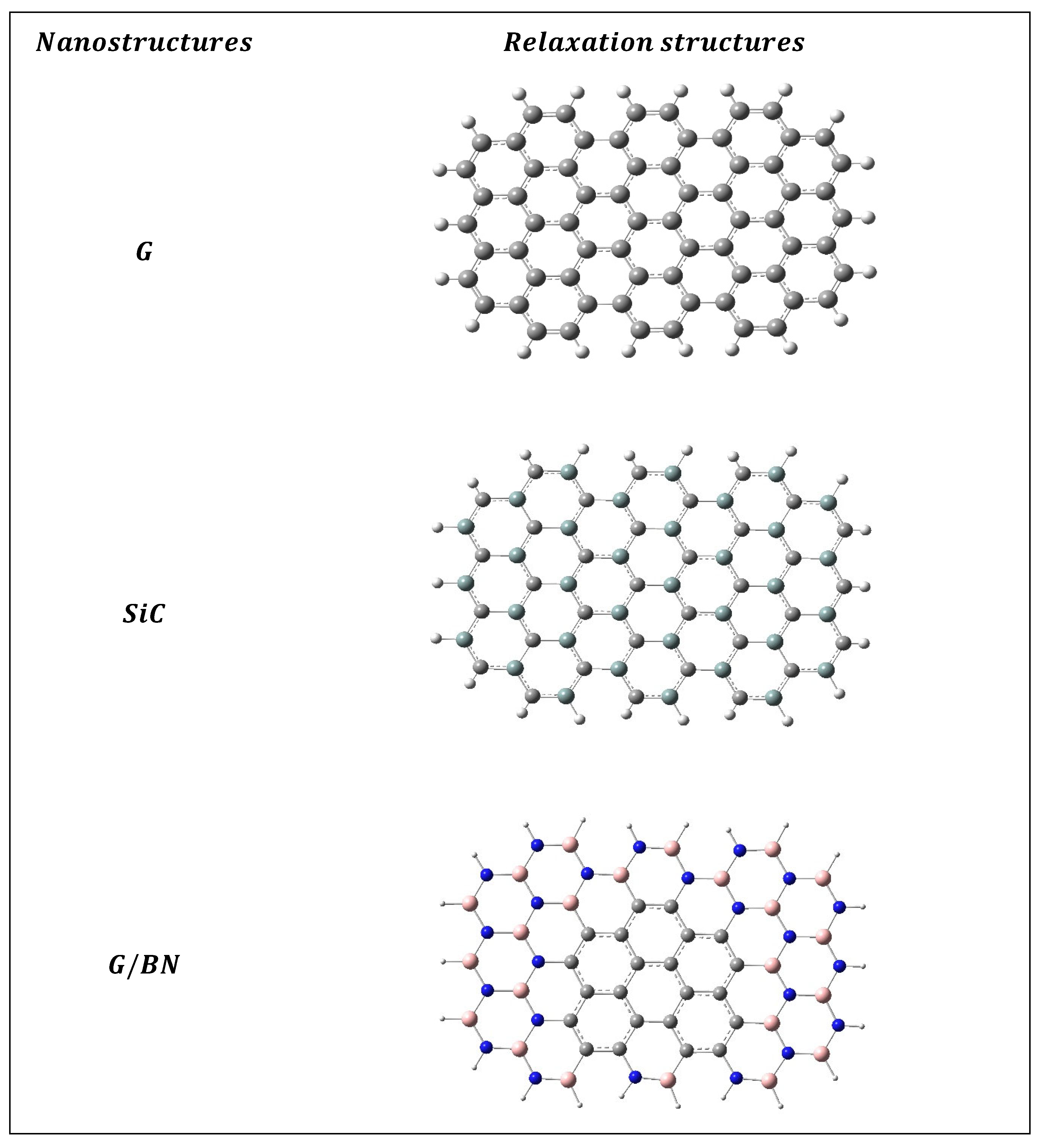
Figure 3.
Distribution of molecular orbital energies around the semiconductor and electrolyte for G, SiC, and G/h-BN nanostructures (isolated phase). A red star (*) indicates that electron regeneration is not possible for G and SiC, while a plus sign (+) indicates successful electron regeneration for G/h-BN.
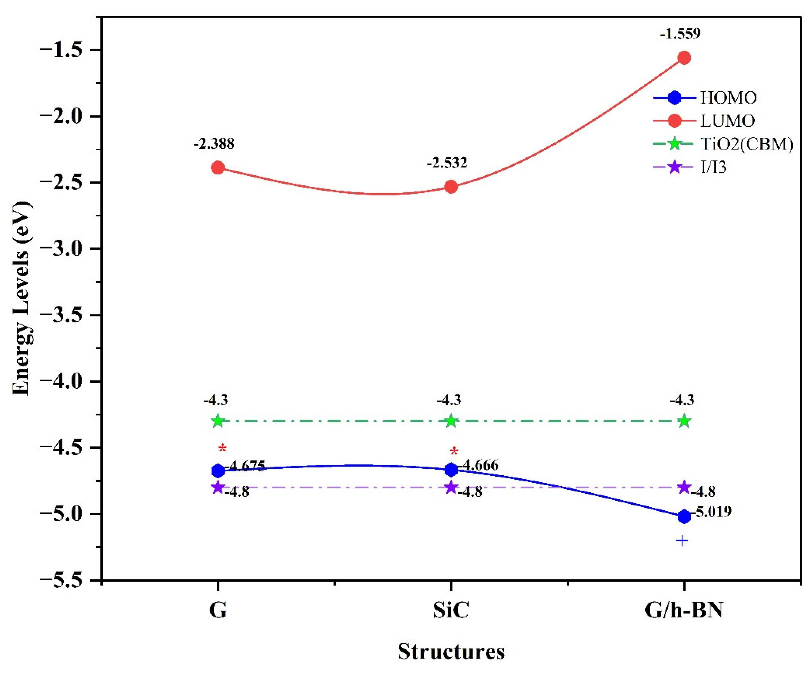
Figure 4.
Illustration of the distribution of molecular orbital energies around the semiconductor and electrolyte for the G, SiC and G/h-BN nanostructures in the isolated case. The plus (+) symbol indicates that the G and SiC nanostructures can regenerate electrons in the ground state so that the solvent DMSO enhances the electronic properties of the G and SiC nanostructures.
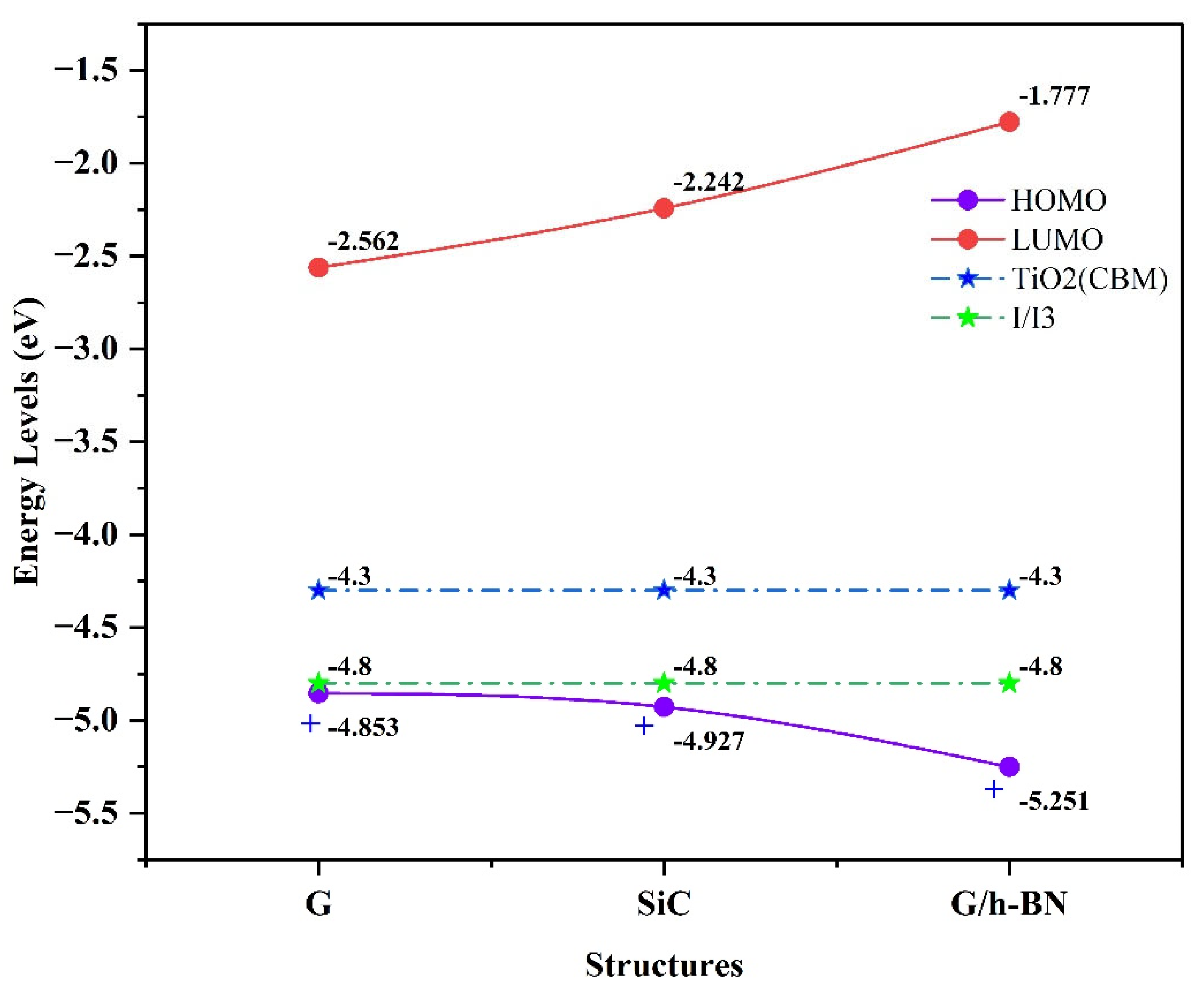
Figure 5.
Bar chart of the computed open voltaic circuit property (Voc) for the isolated and dissolved G, SiC and BN nanostructures.
Figure 5.
Bar chart of the computed open voltaic circuit property (Voc) for the isolated and dissolved G, SiC and BN nanostructures.
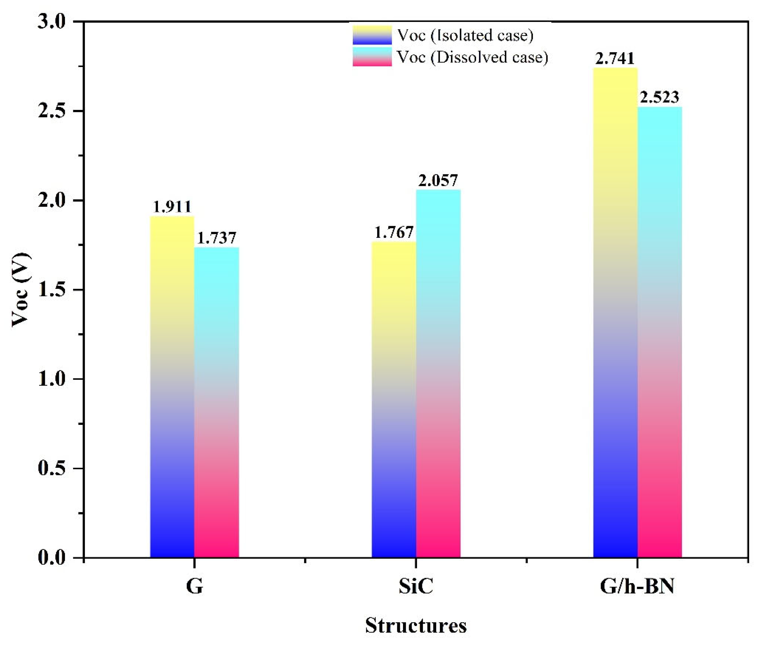
Figure 6.
UV‒Visible spectra of the G, SiC and BN nanostructures in the isolated and dissolved phases. DMSO caused a shift in the UV‒visible spectrum, especially for the G nanostructure.
Figure 6.
UV‒Visible spectra of the G, SiC and BN nanostructures in the isolated and dissolved phases. DMSO caused a shift in the UV‒visible spectrum, especially for the G nanostructure.
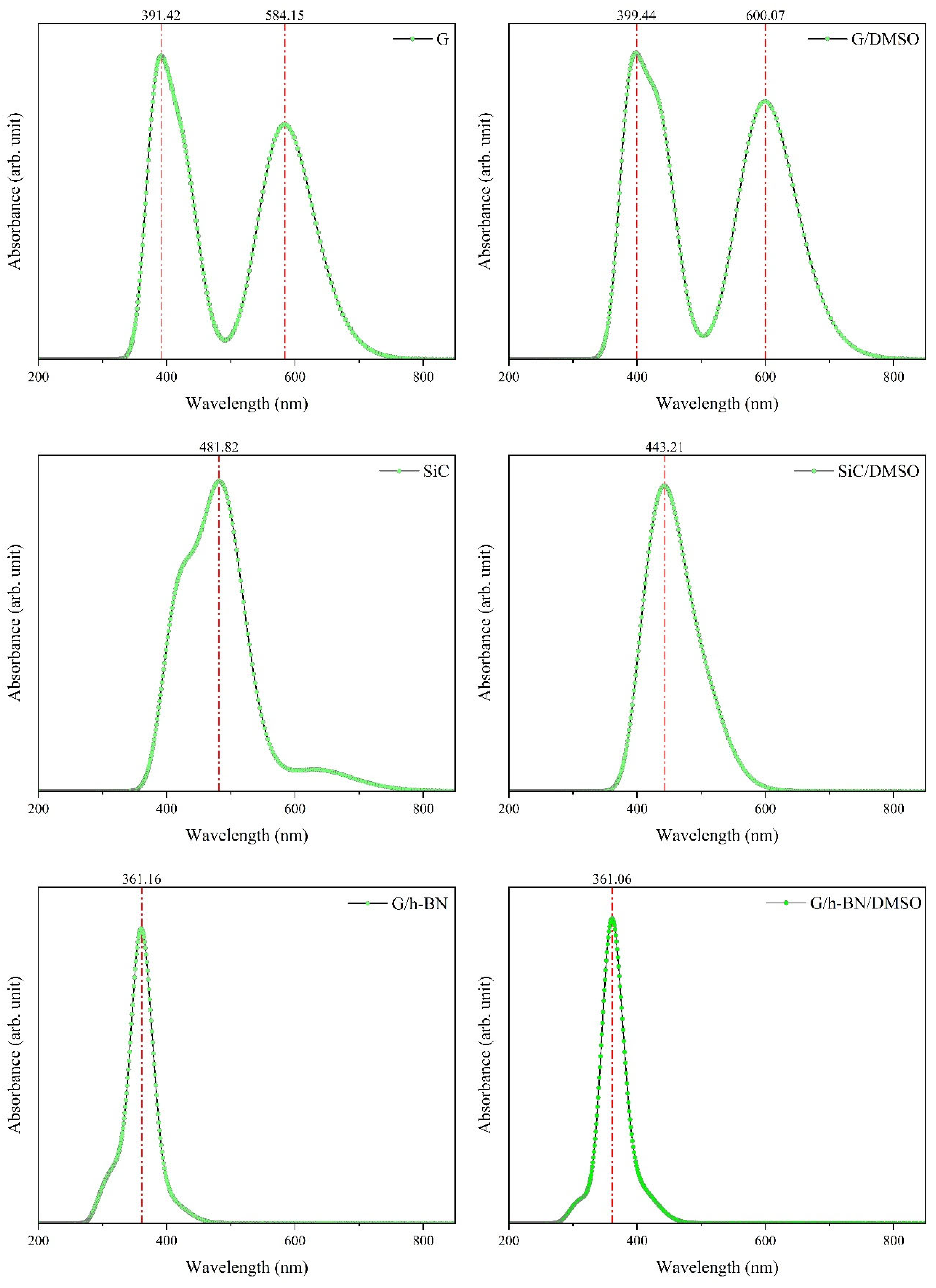
Figure 7.
Bar chart of the LHE properties of the isolated and dissolved G, SiC and BN nanostructures.
Figure 7.
Bar chart of the LHE properties of the isolated and dissolved G, SiC and BN nanostructures.
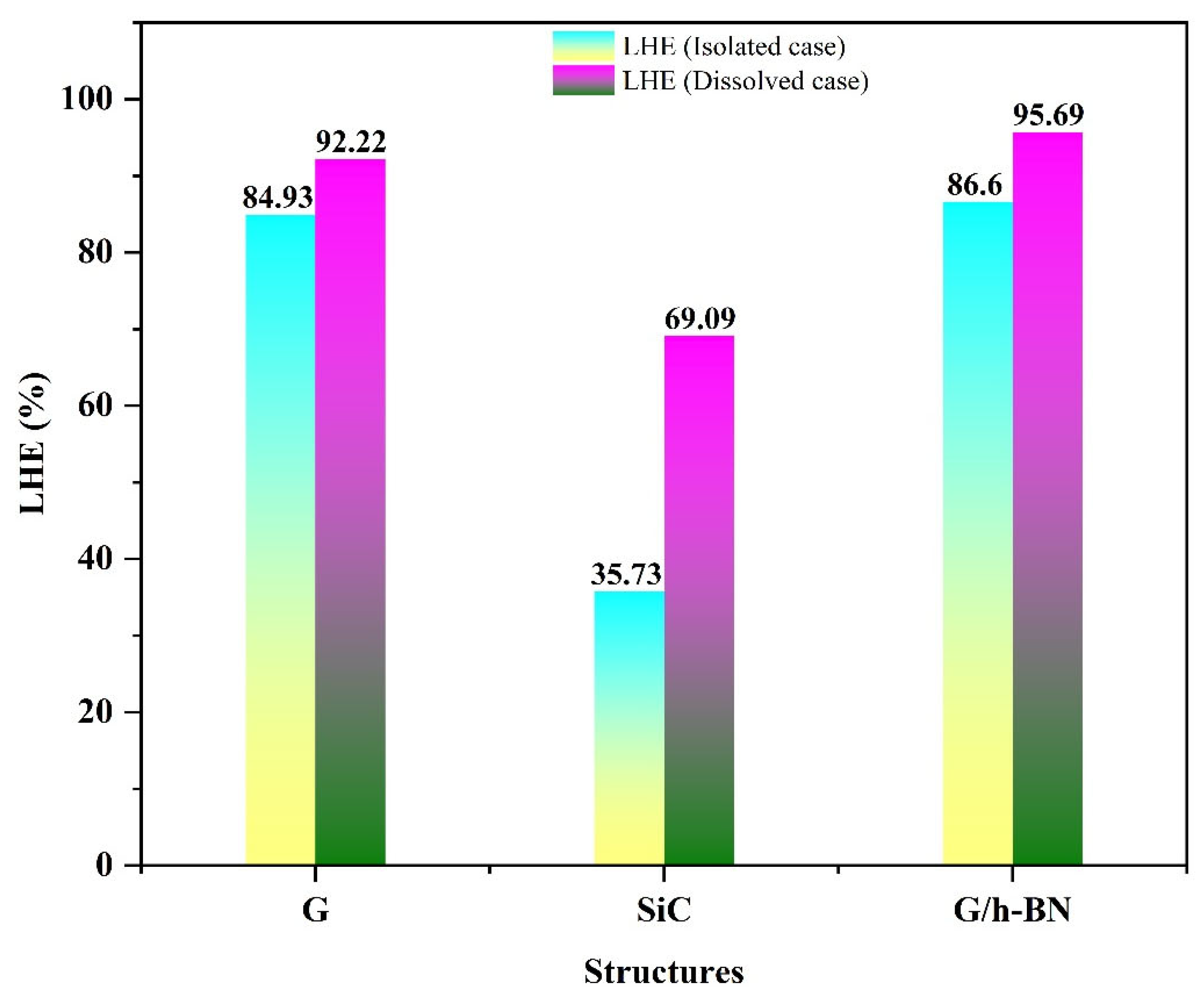
Table 2A.
Indexed molecular orbital energy (EHOMO and ELUMO) and energy gap (Eg) in isolated phase measured in eV.
Table 2A.
Indexed molecular orbital energy (EHOMO and ELUMO) and energy gap (Eg) in isolated phase measured in eV.
|
|
|
|
|
|
|
|
|
|
|
|
|
|
|
|
|
|
|
|
Table 3.
Indicated free energy of electron injection (), free energy of electron regeneration (), open-voltaic circuit (VOC), maximum wavelength of absorption (λmax), excitation energy ( and oscillation strength (f).
Table 3.
Indicated free energy of electron injection (), free energy of electron regeneration (), open-voltaic circuit (VOC), maximum wavelength of absorption (λmax), excitation energy ( and oscillation strength (f).
|
|
|
|
|
|
|
|
|
|
|
|
|
|
|
|
|
|
|
|
|
|
|
|
|
|
|
|
|
|
|
|
|
|
|
|
|
|
|
|
|
|
|
|
|
|
|
|
|
|
|
|
|
|
|
|
|
|
|
|
|
|
Disclaimer/Publisher’s Note: The statements, opinions and data contained in all publications are solely those of the individual author(s) and contributor(s) and not of MDPI and/or the editor(s). MDPI and/or the editor(s) disclaim responsibility for any injury to people or property resulting from any ideas, methods, instructions or products referred to in the content. |
© 2025 by the authors. Licensee MDPI, Basel, Switzerland. This article is an open access article distributed under the terms and conditions of the Creative Commons Attribution (CC BY) license (http://creativecommons.org/licenses/by/4.0/).
Copyright: This open access article is published under a Creative Commons CC BY 4.0 license, which permit the free download, distribution, and reuse, provided that the author and preprint are cited in any reuse.


