
Submitted:
17 June 2025
Posted:
19 June 2025
You are already at the latest version
Abstract
This study presents an innovative modification to the Chemical Bath Deposition (CBD) method for synthesizing zinc oxide (ZnO) thin films by incorporating a high-voltage electric field (HVEF), with and without electrical polarity inversion, to influence film growth dynamics. Two configurations, CBD-HVEF-A and CBD-HVEF-B, were developed to assess the effects of electric field strength, periodic inversion, air agitation, and solution pH on the structural, morphological, and optical properties of ZnO coatings. X-ray diffraction confirmed the formation of the wurtzite ZnO phase, with reduced interplanar spacing and crystallite size under electric fields, especially when polarity was inverted. Scanning electron microscopy revealed that particle size, shape, and distribution were strongly dependent on synthesis parameters, with electric field and air injection enabling higher surface coverage and finer nanostructures. Optical measurements showed a consistent increase in the band gap (blue shift) and reduced defect-related absorption. These findings demonstrate that controlled electric field application during CBD enables precise tuning of ZnO film properties for advanced optoelectronic applications.
Keywords:
Chemical Bath Deposition (CBD)
; electric field-assisted synthesis
; air bubbling-assisted synthesis
; morphological control
; particle size dispersion
1. Introduction
In the modern era, materials science plays a crucial role in technological development, demanding advanced materials with improved performance and sustainability. To achieve these materials with particularly enhanced properties while maintaining their cost-effectiveness, it has been essential to improve and develop the synthesis techniques used to obtain them [1,2,3,4].
Chemical Bath Deposition (CBD) is a solution-based technique for growing thin films on substrates by immersing them in an aqueous solution containing the desired chemical constituents [5]. The thin film forms through a heterogeneous surface reaction, meaning a chemical reaction occurs at the solid-liquid interface. While conceptually similar to Chemical Vapor Deposition (CVD), CBD operates in a liquid medium instead of a vapor phase. Typically carried out in a simple beaker as a batch process, CBD involves both heterogeneous (on the surface) and homogeneous (in the solution) reactions, with bath conditions changing over time due to chemical consumption and byproduct formation. It can even produce epitaxial layers on single crystal surfaces. CBD is widely used to deposit various semiconductor thin films such as CdSe, Cu2S, ZnO, ZnS, and TiO2 [6,7,8,9] , and holds particular significance in solar cell applications. The advantages of CBD include low cost due to inexpensive chemicals and simple equipment, ease of implementation and control, scalability for large-area deposition, flexibility in tuning film properties through solution composition and deposition conditions, the ability to produce good-quality films, versatility in applying it to a wide range of materials including quantum dots and nanoparticles, and the lack of need for complex instrumentation typically associated with vacuum-based methods [10,11]. Compared to other techniques like CVD, RF sputtering, vacuum deposition, atomic layer deposition, and electrodeposition, CBD is significantly cheaper and simpler to set up and operate, does not require vacuum systems or high-energy sources, is easier to scale for industrial use, has a faster and more straightforward process, and is better suited for temperature-sensitive substrates due to its typically lower operating temperatures [12,13,14]. In summary, Chemical Bath Deposition is a cost-effective, simple, and versatile method for synthesizing high-quality thin films and nanostructures, offering a strong potential especially in solar energy and nanomaterial applications, with its main advantage being the balance of quality and simplicity without the need for expensive infrastructure.
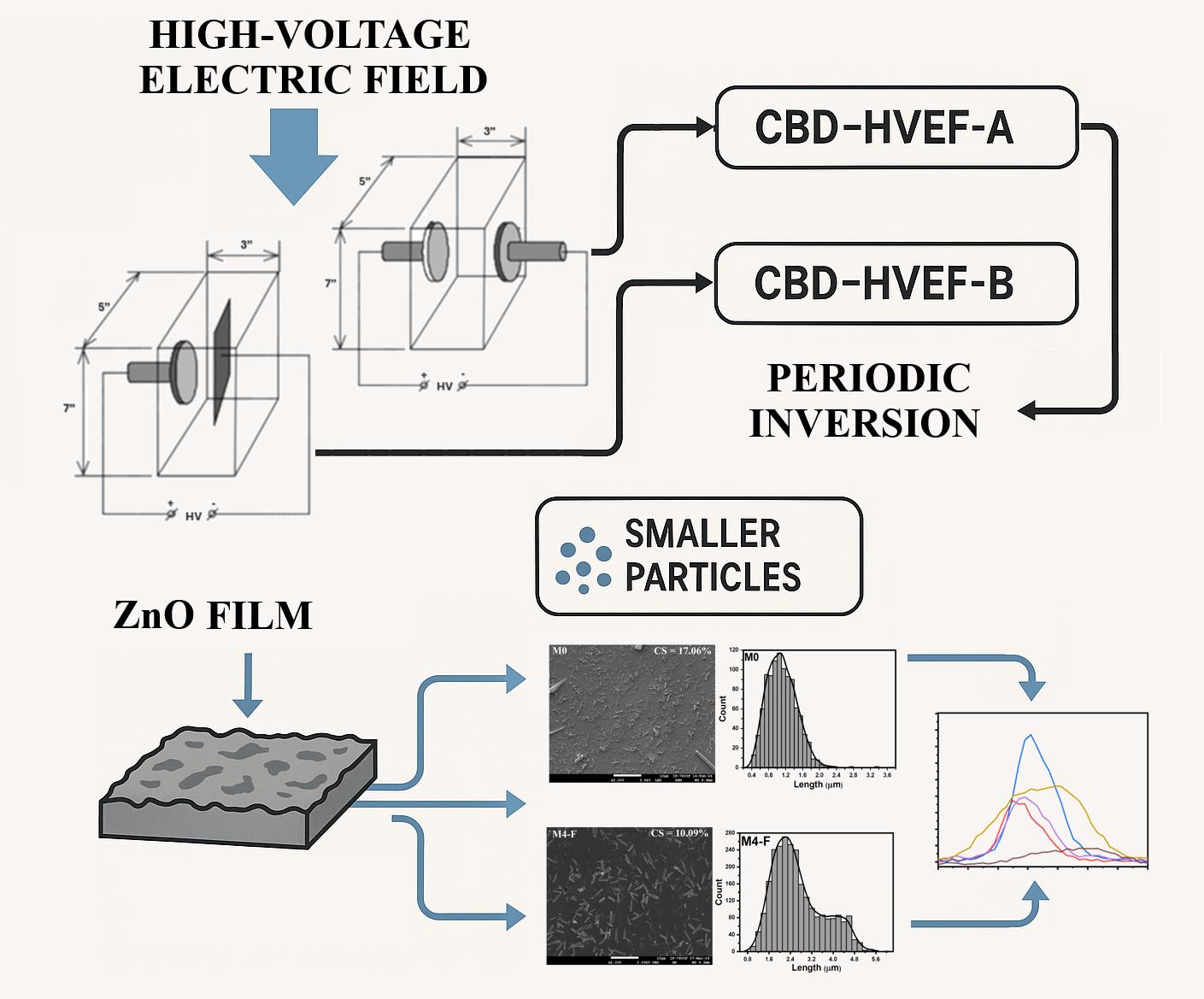
Thus, the present work proposes an innovation on conventional CBD technique by implementing the use of a high-voltage power supply whose output voltage can be controlled, allowing the application of both uninterrupted DC voltage and high voltage pulses of controlled frequency, this is to assist the synthesis process with a high voltage electric field. Two configurations were designed for the experiments: CBD-HVEF-A and CBD-HVEF-B, presented in Figure 1; additionally, to evaluate the effect of the applied electric field on properties of the synthesized coatings, both configurations were utilized for the synthesis of ZnO coatings, as synthesis by CBD of this semiconductor has been widely studied by several research groups in the last decade [15].
2. Experimental Details
2.1. Synthesis
Two groups of ZnO samples were synthesized, the first group using CBD-HVEF-A system, where the synthesis was assisted by using an electric field induced by parallel plates placed on the opposite outer surfaces of the container, while for the second group CBD-HVEF-B was employed where the electric field was established by considering a plate placed on the outer surface of the container as the first electrode and an ITO-coated glass substrate immersed in the solution as the second. Figure 1 shows the configuration of each system and the way in which the substrate was placed inside the glass container. Both types of substrates, glass and ITO-coated glass, were immersed vertically in the precursor solution for all experiments.
The precursor solution used to carry out the synthesis of ZnO was composed of: 910 ml of double distilled water, 6.39 g of Zinc Acetate dihydrate (AcZn, J.T Baker) and 4.08 g of Hexamethylenetetramine (HMTA, J.T Baker) to reach a concentration of 0.032 M and a constant molar ratio of 1:1 between AcZn and HMTA. In the case of the precursor solution of the CBD-HVEF-B system, potassium hydroxide (KOH, Macron Fine Chemicals) was used to achieve pH values in the range of 6.87-8.98.
In order to study the possible effects that the electric field and its intensity variation could have on the morphology, crystalline structure and optical properties of ZnO coatings, electric field intensity was varied by varying the voltage between the parallel metal plates (CBD-HVEF-A) or between the ITO substrate and the metal plate (CBD-HVEF-B). The voltage values in CBD-HVEF-A were 0, 24, and 36 kV while in CBD-HVEF-B the values were 0, 24, 30 and 36 kV. In both systems the V = 0 kV corresponds to the conventional CBD. Furthermore, two ZnO coatings were synthesized by periodically reversing the electrical polarity in CBD-HVEF-A at two different periods: 2.5 and 10 minutes and maintaining a voltage of 36 kV. The electrical polarity reversal was performed manually using the device shown in Figure 1a.4. In CBD-HVEF-B, in addition to the applied electric field, filtered air was injected into the precursor solution during the synthesis process, in order to study the effect of both on the morphology of the coating. The air was injected using a conventional 5 W fish tank pump that had an air filter attached.
Table 1 and Table 2 listed the samples that were synthesized by CBD-HVEF-A and B, respectively, considering the synthesis parameters for each of them.
The temperature of the precursor solution for samples synthesized using CBD-HVEF-A system was measured every 15 minutes using a Craftsman model 50466 infrared thermometer to maintain, through the IKA ® C-MAG HS 7 hotplate, a constant temperature within a range of 79.8 ± 2.8 °C. When the synthesis was performed using the CBD-HVEF-B system, the pH and temperature of the precursor solution were measured every 15 minutes using a pH/ORP meter of Hanna Instruments model HI 2211, turning off the voltage source each time the measurement was taken.
After deposition, substrates were removed, thoroughly rinsed with deionized water and dried with hot air. The time of synthesis was 3 hours for all coatings.
2.2. Characterization
The crystalline structure of all samples was obtained by X-ray diffraction using a BRUKER D8 ADVANCE diffractometer with a step of 0.03350 degrees. Morphology and chemical composition were obtained by using a JOEL JSM-7600F scanning electron microscope. Transmittance spectra of the ZnO films were obtained by using a Variant Cary 5000 UV-VIS-NIR spectrometer.
3. Results and Discussion
3.1. Films Deposited by CBD-HVEF-A
3.1.1. X-Ray Diffraction
To confirm that the material obtained using CBD-HVEF-A system is in fact ZnO, as well as the possible influence of the electric field in the resulting crystal parameters, the XRD patterns of all samples were obtained. Figure 2a presents diffraction patterns for samples M0, M1-F, M2-F, M3-F and M4-F, all of which were indexed to crystallographic card JCPDS No. 076-0704, corresponding to the hexagonal wurtzite phase of ZnO. All samples show preferential growth in the (100) direction, with this peak being the most intense for all cases. Figure 2b and c show close-ups of two different regions of the XRD patterns corresponding to peaks (100), (101) and (002), where at first glance, a significant shift in diffraction angles can be observed.
For closer examination on angle shift and possible broadening of the peak (100) for all samples, Figure 2-d and e present its gaussian fit, which was also normalized by each maximum and its corresponding baseline was subtracted, even when for sample M4-F, this approximation is very optimistic, as it is evidently conformed by two diffraction peaks as seen in Figure 2c which may indicate the formation of two kinds of crystalline grains. It can be observed that the diffraction angles for samples M1-F and M2-F are shifted to the right when comparing them to sample M0 which had no electric field applied. This shift signals a reduction in the interplanar distance of (100) planes for these samples. Therefore, one could state that the application of an electric field during synthesis can result in a reduction of interplanar distance, which is bigger when a higher voltage between plates is used, as is the case of M1-F.
When maintaining a constant voltage of 36 kV but periodically inverting the direction of the electric field, an inspection of peak (100), which is also the most intense for samples M3-F, and M4-F, shows that there is both a shift in the diffraction angle and a broadening of all peaks compared to sample M1-F, which has the same synthesis conditions but no inversion of electric field. For higher inversion frequency, sample M3-F, there is a major broadening of the diffraction peak, which implies a smaller grain size, along with a reduction in the interplanar distance between (100) planes, as indicated by the shift in its diffraction angle, this also occurs for sample M4-F, although for this case, grain size reduction is still significant but less than that of M3-F, with an even smaller interplanar distance, Table 3 shows the calculated values for interplanar distance and grain size for all samples, considering peak (100), where it is even more evident how polarity inversion of the electric field promotes a decrease in interplanar distance along with a big reduction of grain size to around half of the value obtained by no inversion.
3.1.2. SEM
The analysis of SEM micrographs of the samples shows that the surface of all films is formed by bar-shaped particles of micro or nanometric dimensions, as well as notable differences in said dimensions, according to the deposition conditions listed in Table 1.
Figure 3 presents micrographs for all samples, as well as their corresponding size distribution functions of the ZnO bars that constitute each sample. It is evident that not all of the substrate surface is evenly coated in said ZnO bars, therefore, a quantitative measure of the covered surface (CS) was done via a program designed in Mathematica Software [16], the corresponding obtained values are inserted in each micrograph.
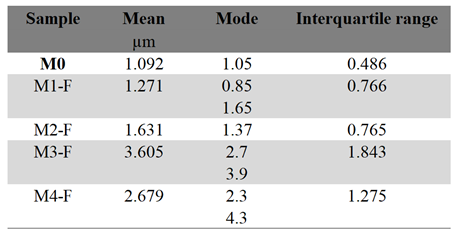
Table 4 presents the descriptive statistics that summarize the information from the distribution function graphs. The distribution function along with the cumulative curves for these samples show that the application of an electric field results in a dispersion and increasing of the bar sizes, as mean size went from 1.092 µm in sample M0 with no electric field applied, to 1.271 µm and 1.631 µm for samples M1-F (36 kV) and M2-F (24 kV), respectively; and interquartile went from 0.486 um for sample M0 to ≈0.76 in both M1-F and M2-F samples in which electric field was applied, meaning that although dispersion in the bar size increased with the electric field, the value is the same even with two different electric field intensities.
As for samples M3-F and M4-F, the electric field was maintained at 36 kV but inverting its polarity every 2.5 and 10 minutes, respectively. When looking at their SEM images, the resulting particles maintain the same bar structure as other samples, although a quick glance at the average particle size confirms that in both cases, these bars are considerably larger comparing them to M1-F where no inversion of electric field occurred, being M3-F modes larger in a ratio of 3.17:1 and 2.36:1 as well as 2.70:1 and 2.61:1 for M4-F. Moreover, both samples maintain the bi-modal distribution function from sample M1-F, which is a good indicative of consistency in the synthesis process. The interquartile range allows to see that the dispersion in the bar size increases further with the polarity inversion in electric field, resulting bigger in M3-F which has a higher inversion frequency (shorter period), which is in agreement with the fact that longer periods should behave as if no inversion occurs.
Figure 4 presents the cumulative curves of the length of the ZnO bars for all samples, where a higher slope indicates a lower dispersion of the bar lengths and the apparition of more than one linear segment is a consequence of multi-modal distribution functions and the number of segments indicates the number of modes. This being said, the application of an electric field during the synthesis of ZnO results in higher dispersion rates and bi-modal functions. The slope values of each cumulative curve are inserted in the figure in order to show a quantitative measure of the length dispersion. These curves make even more evident what was stated above: the application of an electric field results in an increase of particle length in all cases, to a greater degree for samples with inversion of polarity.
3.1.3. Transmittance
Figure 5 presents the transmittance spectra for all samples, the values of their respective intraband absorption are summarized in a table inserted in the same figure. These intraband absorption values were obtained through the first and second derivatives of the absorbance curves. There is an evident blue-shift of ~5 nm in all samples as an effect of the applied electric field during synthesis, with the exception of M4-F, where a slight red-shift of ~2 nm occurred. This blue shift of ~5 nm indicates an increase of the same order in the band gap of the material as a result of the electric field applied independently of its intensity or if its polarity was inverted. As for M4-F the almost imperceptible red-shift of ~2 nm indicates a slight decrease in its band gap, although this is not in agreement with the tendency followed by the rest of the samples, this could be justified by looking at its XRD pattern presented above, where M4-F also presents the apparent formation of two kinds of crystals with different interplanar (100) distance, predominantly crystals with a lower interplanar distance.
What is said in the previous paragraph is congruent with the angle shift observed in the XRD patterns, since a lower interplanar distance translates into a higher crystalline field, which will increase the band gap of a material.
Regarding the absorption of ZnO in the visible spectrum, commonly associated with the presence of defects in its crystalline structure, it is observed that while sample M0 deposited by conventional CBD presents an absorption that begins at 550 nm and becomes more intense as it approaches the blue, none of the samples grown by CBD-HVEF-A present this absorption (see Figure 5). This absorption is commonly associated with oxygen defects and/or interstital zinc [17], so in principle it can be observed that deposition by CBD-HVEF-A inhibits the formation of these types of defects. When comparing the transmittance spectra of the samples grown by CBD-HVEF-A, it is clear that sample M1F is the one that in principle presents the fewest defects in its crystalline structure, since it only presents a slight absorption centered at 2.05 eV, which is commonly associated with the presence of hydroxyl (OH) groups as an emission center, particularly present in synthesis methods involving aqueous solutions [17], while M2-F, M3-F and M4-F presented, in addition to this absorption, an absorption centered at 1.59 eV, commonly associated with hydrogen impurities [18,19,20].
3.2. Films Deposited by CBD-HVEF-B
Figure 6 presents micrographs for samples obtained using the CBD-HVEF-B system, each labeled according to the corresponding sample listed in Table 2. These micrographs showed homogeneity in the ZnO deposit as well as the fact that all the coatings were composed of nanometric-sized particles, except for M0a-S, which is the sample deposited by conventional CBD technique and was composed of submicrometric particles. Each micrograph has an insert with the percentage value of the substrate area coated by ZnO, obtained by a software developed by our research team, and employed in previous reports [16]. The characteristic shape of the particles and the descriptive statistics of their sizes are presented in the table inserted in Figure 7. The same figure also shows the particle size distribution functions for all the coatings, in correspondence with the micrographs in Figure 6. There, next to each of the size distribution functions, their corresponding cumulative size curves are presented. The comparative analysis between the coatings, in terms of the shape and size of the particles that compose them, was carried out based on whether or not an electric field was used during the synthesis and whether or not the solution was stirred by injecting filtered air into it, in addition to the variation in its pH, thus resulting in eight comparative analyses between the coatings. Figure 8 shows the different cumulative size curves of the coatings according to the comparative analysis in question. Likewise, Figure 9 and Figure 10 show the temperature and pH curves of the solution during synthesis process, corresponding to each comparative analysis in Figure 8, this is in order to assess whether or not there are significant differences between the temperature and pH curves that should be considered for the corresponding analysis.
The comparison between micrographs of samples M0a-S and M2-S, figures 6a and 6d, respectively, clearly shows the influence of the electric field during the CBD synthesis process. It can be observed that the conventional CBD coating M0a-S covers only 10.33% of the ITO substrate surface, while the coating whose synthesis was assisted by the electric field (M2-S) covers 99.66% of the surface, as well as that the particles that make up the coating went from being bars of dimensions in the order of 247 nm with very well-defined edges in M0a-S to particles with rounded edges and practically no defined corners, the average dimensions for M2-S was 40.71 nm with a mode of 33.69 nm, thus reducing its size by 6 times (see table inserted in Figure 7). This reduction in particle size is even better appreciated by comparing the cumulative size curves for both coatings, see Figure 8a. Now, on the other hand, when comparing the micrographs for M0a-S and M0b-S coatings, figures 6a and 6b, respectively, both synthesized without an electric field, it can be seen that stirring the solution with injection of filtered air during the synthesis process has the effect of reducing the size of the particles that make up the coating, same effect as exposed above for when an electric field is applied, but in this case the particles achieved a greater reduction, up to 12 times their size, resulting in an average size of 29.90 nm and a mode of 19.45 nm (see table inserted in Figure 7), in addition to retaining the morphology of bars with very well-defined edges, most of them growing perpendicular to the substrate surface, however; the area of the substrate that was covered by ZnO was smaller, around 60.46 %. In summary, applying an electric field or stirring the solution through the injection of filtered air led to a higher growth rate of ZnO and a reduction in the size of the particles that make up the coating, in addition to the fact that the electric field promoted the aggregation of the nanoparticles, which resulted in a much more compact coating.
Micrographs associated with coatings M1-S, M2-S and M3-S (figures 6c,d and e) were compared to study the effect of the electric field intensity on the coating morphology, this for electric fields produced by potential differences between electrodes of 24, 30 and 36 kV, respectively. It was observed that the morphology of the coatings was similar, independent of the field intensity, observing a nodular type growth followed by a coalescence process between particles. The degree of aggregation of the particles, as well as the percentage of the covered substrate area were greater for 30 kV, covering up to 99.66% of the substrate surface, while for 24 and 36 kV it was 88.31 and 58.22%, resulting in a coating with greater compactness for 30 kV. When comparing the cumulative particle size curves, Figure 8b, it is observed that the particle size grows slightly by 16.9 % when the potential difference goes from 24 to 36 kV as well as a variation in the dispersion of their sizes, the latter is noticeable by the relative change in the slope of the curves (see values in the same figure), the dispersion being lower for 30 kV where the slope of the curve is greater, which is consistent with its interquartile range of 13.56 nm (see table in Figure 7), while for the coatings obtained at 24 and 36 kV, the interquartile range was 18.66 and 15.91 nm, respectively.
To study the effect that the intensity of the electric field in combination with the injection of filtered air has on the coating morphology, micrographs for M4-S, M5-S and M6-S were compared for 36, 30 and 24 kV, respectively (see Figure 6). It is observed that the nanoparticles that make up the coating seem to be composed of smaller particles with well-defined edges, which suggests a columnar type growth, unlike the nodular growth observed when only the electric field is applied. Likewise, it is also observed that the coating that now presents greater compactness is the one obtained at 36 kV and not at 30 kV as it was when the solution was not stirred with filtered air, and that the substrate coverage reached up to 91.79% for 36 kV, while for 30 and 24 kV it was 46.36 and 75.64%, respectively. Figure 8c presents the cumulative size curves for the three coatings, as well as the curve for the one in which only air injection was applied (M0b-S), as can be seen, applying an electric field in addition to air injection has the effect of increasing the average particle size in such a way that when its intensity is increased this effect is even greater, going from an average size of 26.5 nm for a field produced by 24 kV to 31.5 nm for that produced by 36 kV, the same also occurs with the size dispersion, as can be seen through the decrease in the slope of the curve as the field intensity increases (values are in the same figure), going from 4.99 to 3.19 for 24 and 36 kV respectively.
To further highlight the effect that applying an electric field and air injection have together on the average particle size that constitute the coating and the dispersion of their sizes, Figure 8e presents the cumulative size curves for the M0b-S, M2-S and M5-S coatings, which synthesis was assisted by: air injection in M0b-S, electric field produced by a voltage of 30 kV between electrodes in M2-S and electric field of 30 kV in addition to air injection in M5-S. These cumulative curves show how the effects of the electric field and the air injection on the size of the particles that make up the M5-S coating overlap, giving rise to a film made up of nanoparticles with an average size of 35.33 nm and a mode of 27.50 nm, which are intermediate values between the average sizes and modes values for when only air injection is applied (M0b-S): 29.90 nm and 19.45 nm and when only electric field is applied (M2-S): 40.71 nm and 33.79 nm. Likewise, figures 8d, e and f show how the effect of the electric field on the size of the particles is shielded by the effect that air injection has on them. It is observed that as the intensity of the electric field is reduced, the size of the particles becomes increasingly similar to that obtained by only injecting filtered air into the precursor solution. Now, regarding the morphology of the coating, it is observed that applying an electric field, in addition to air injection, does not affect the columnar type growth that ZnO presents with only air injection, it is even also possible to observe the perpendicular growth of the bars with respect to the substrate surface in the M5-S coating (30 kV) for which the coverage of the substrate surface was lower, around 46.38%. In the M6-S (24 kV) and M4-S (36 kV) coatings, the amount of material deposited on the substrate is such that the growth of bars perpendicular to the surface cannot be seen.
To determine the effect of the pH of the precursor solution on the coating morphology and particle size that comprise it, a comparison was made between micrographs M1-S vs M7-S and micrographs M2-S vs M8-S that were synthesized only under the influence of an electric field and at the same synthesis conditions between them, except for the pH of the solution, which between the coatings M1-S and M7-S, synthesized at 24 kV, had a pH difference of up to 2.5 (Figure 8g), while between M2-S and M8-S, synthesized at 30 kV, the pH difference was never greater than 1 (Figure 8h). In both comparisons it is observed that when the pH decreases the coalescence between the particles that make up the coating decreases notably to such an extent that it is practically imperceptible, in addition to the fact that the average size of the particles that make up the coating practically does not change, however, the dispersion of the particle sizes decrease notably when the pH decreases to such an extent that the solution goes from alkaline to acidic, which can be seen in Figure 8g with the significant increase in the slope of the cumulative size curve for M7-S with respect to M1-S.
As a general discussion, we propose that the growth conditions employed in our ZnO thin film system exert a significant influence on coalescence and, consequently, on film compaction. These phenomena are directly correlated with the attainment of crystallinity, crystallite size, and surface morphology. Coalescence refers to the process wherein particles merge to form a continuous film, evidently affecting both morphological features and the structural crystallinity of the film. Meanwhile, film compaction, related to density and absence of porosity, can impact transparency and optical properties.
X-ray diffraction (XRD) analysis revealed that the application of an electric field and polarity inversion induced a reduction in interplanar spacing and an enhancement of crystallinity, suggesting increased coalescence of crystallites. This is further reflected in the reduced crystallite size, implying a higher density of defects, although the improved crystallinity may mitigate some of these effects.
Regarding crystallite size, the CBD-HVEF-B configuration at 30 kV achieved a higher degree of coalescence and substrate coverage, resulting in a more compact film with minimal particle size dispersion. Scanning electron microscopy (SEM) confirmed that the combination of electric field application and air agitation produced a mixed morphology featuring both nodular and columnar characteristics, alongside enhanced substrate coverage. Future studies could explore residual stresses, surface strain, and electrical properties [21].
4. Conclusions
About the properties of coatings synthesized using CBD-HVEF-A.
The structural, morphological, and optical analyses presented in this study confirm that the material synthesized via the CBD-HVEF-A system is indeed ZnO with a hexagonal wurtzite crystalline phase. The application of a high-voltage electric field during synthesis exerts a marked influence on both the crystallographic and morphological characteristics of the ZnO films.
XRD analysis reveals that the electric field not only modifies the diffraction angles, indicating a reduction in interplanar spacing of the (100) planes, but also leads to significant peak broadening in samples subjected to electric field polarity inversion. These observations imply the formation of smaller crystallites and possibly multiple crystalline phases in certain cases, especially for M4-F, where dual peak characteristics suggest the coexistence of grains with distinct interplanar distances.
Morphological inspection via SEM demonstrates that all ZnO films consist of bar-shaped particles whose size distribution is highly dependent on the applied electric field conditions. The presence of the field promotes an increase in average particle length and dispersion, and polarity inversion further intensifies this effect. Notably, samples synthesized under periodic field inversion show larger particle dimensions and broader interquartile ranges, consistent with a frequency-dependent modulation of growth dynamics. The emergence of bimodal and multimodal distribution functions in these samples also suggests enhanced complexity in nucleation and growth under field inversion.
Optical measurements show a consistent blue-shift in the transmittance edge (~5 nm) across most samples synthesized with the electric field, indicating an increase in the band gap, likely due to reduced interplanar spacing and enhanced crystalline order. An exception is sample M4-F, which exhibits a slight red-shift, potentially attributable to the presence of dual crystalline domains with different lattice parameters.
Moreover, visible-range absorption data suggest a notable reduction in defect-related absorption bands for all samples synthesized via CBD-HVEF-A compared to conventional CBD, indicating a suppression of oxygen vacancies and interstitial zinc. Among these, sample M1-F exhibits the lowest defect concentration, with minimal absorptive features, while other samples show signatures of hydrogen- and hydroxyl-related impurity states.
In summary, the application of a high-voltage electric field, particularly with periodic polarity inversion, profoundly alters the structural, morphological, and optical properties of ZnO films grown by CBD. These findings not only provide a deeper understanding of electric field-assisted synthesis mechanisms but also open new avenues for tailoring ZnO properties for optoelectronic applications through controlled field modulation.
About the properties of coatings synthesized using CBD-HVEF-B.
From the comparative analysis of micrographs and the morphological characterization of the ZnO coatings synthesized using the CBD-HVEV-B system, the following conclusions are drawn:
Influence of the electric field: The application of an electric field during the synthesis process has a significant effect on substrate coverage and particle morphology. In particular, a considerable increase in the coated area (up to 99.66%) and a decrease in the average particle size (up to 6-fold reduction) were observed compared to conventional synthesis without an electric field.
Effect of air injection stirring: Agitating the precursor solution by injecting filtered air also promotes the formation of smaller particles (up to a 12-fold reduction), albeit with less coverage of the substrate. Furthermore, this technique induces a columnar morphology with preferential growth perpendicular to the substrate, preserving the bar-like shape with well-defined edges.
Combination of electric field and air injection: The synergy between electric field and air injection has a cumulative effect on particle size, resulting in intermediate size nanoparticles compared to those obtained with each technique alone. This combination favors a mixed morphology with both nodular and columnar characteristics, depending on the field strength.
Variation in electric field intensity: It was determined that a potential difference of 30 kV produces more compact coatings with less particle size dispersion, which translates into greater morphological uniformity. Higher or lower intensities (24 and 36 kV) showed less coverage and greater dispersion.
Effect of solution pH: Decreasing pH, especially when moving from alkaline to acidic conditions, inhibits particle coalescence without significantly affecting their average size. However, the size dispersion is significantly reduced, suggesting greater control over coating uniformity under acidic conditions.
Morphological control through synthesis parameters: The results show that the morphology, size, and distribution of ZnO nanoparticles can be precisely controlled by modulating three main parameters: electric field intensity, air injection agitation, and solution pH. This allows the coating properties to be tailored to specific requirements in technological applications.
References
- Wilson, N. Advancements in Material Synthesis Techniques and their Implications. Material Sci Eng 2024, 13, 694. [Google Scholar] [CrossRef]
- Schmidt, R.; Gonjal, J.P.; Morán, E. Microwave-Assisted Hydrothermal Synthesis of Nanoparticles. In CRC Concise Encyclopedia of Nanotechnology; T. &. F. Group, Ed., Boca Ratón, Florida, USA, CRC Press, 2016, pp. 561–572.
- Tang, B.; Lu, Y.; Zhou, J.; Chouhan, T.; Wang, H.; Golani, P.; Xu, M.; Xu, Q.; Guan, C.; Liu, Z. Machine learning-guided synthesis of advanced inorganic materials. Materials Today 2020, 41, 72–80. [Google Scholar] [CrossRef]
- Muhammand, T. Advanced fabrication techniques for polymer–metal nanocomposite films: State-of-the-art innovations in energy and electronic applications. Chemical Sci 2025, 16, 3362–3407. [Google Scholar] [CrossRef]
- Schneller, H.; Waser, R.; Kosec, M.; Payne, D. Chemical Solution Deposition of Functional Oxide Thin Films; New York Dordrecht London: Springer Wien Heidelberg, 2013.
- Hodes, G. Semiconductor and ceramic nanoparticle films deposited by chemical bath deposition. Phys. Chem. Chem. Phys. 2007, 9, 2181–2196. [Google Scholar] [CrossRef] [PubMed]
- Strano, V.; Greco, M.G.; Ciliberto, E.; Mirabella, S. ZnO Microflowers Grown by Chemical Bath Deposition: A Low-Cost Approach for Massive Production of Functional Nanostructures. Chemosensors 2019, 7, 62. [Google Scholar] [CrossRef]
- Hodes, G. Semiconductor and ceramic nanoparticle films deposited by chemical bath deposition. Phys. Chem. Chem. Phys. 2007, 9, 2181–2196. [Google Scholar] [CrossRef]
- Sagadevan, S.; Das, I. Chemical bath deposition (CBD) of zinc selenide (ZnSe) thin films and characterisation. Australian Journal of Mechanical Engineering 2017, 15, 222–227. [Google Scholar] [CrossRef]
- Oliva, A.I.; González-Chan, I.J.; Várguez, P.E.; Trejo-Ramos, A.I.; Oliva-Avilés, A.I. The chemical process for materials deposition in aqueous solution: A review. Surface Engineering 2022, 38, 907–929. [Google Scholar] [CrossRef]
- Guire, M.; Bauermann, L.; Parikh, H.; Bill, J. Chemical Bath Deposition. In Chemical Solution Deposition of Functional Oxide Thin Films; Illinois, USA, Springer, 2013, pp. 319–339.
- Wangab, X.; Hu, W. Polydopamine thin film-assisted patterned chemical bath deposition of ZnO nanorods on arbitrary substrates. CrystEngComm 2017, 19, 6182–6188. [Google Scholar] [CrossRef]
- Arsad, A.Z.; Zuhdi, A.W.M.; Abdullah, S.F.; Chau, C.F.; Ghazali, A.; Ahmad, I.; Abdullah, W.S.W. Effect of Chemical Bath Deposition Variables on the Properties of Zinc Sulfide Thin Films: A Review. Molecules 2023, 28, 2780. [Google Scholar] [CrossRef] [PubMed]
- Mari, G.M.D.; Matta, V.L.; Strano, V.; Reitano, R.; Cerruti, P.; Filippone, G.; Mirabella, S.; Bruno, E. Optimized Chemical Bath Deposition for Low Cost, Scalable, and Environmentally Sustainable Synthesis of Star-Like ZnO Nanostructures. ACS Omega 2024, 9, 38591–38598. [Google Scholar] [CrossRef] [PubMed]
- Toma, F.; Rahman, M.; Maria, K. A review of recent advances in ZnO nanostructured thin films by various deposition techniques. Discov Mater 2025, 5, 60. [Google Scholar] [CrossRef]
- López-Esmerio, C.; Ruiz-Rojas, C.; Angulo-Rocha, J.; Lizárraga-Medina, E.; Ramos-Brito, F.; Camarillo-García, E.; Martinez-Martinez, R.; Aguilar-Frutis, M.; García-Hipólito, M. Study of the Electrical, Optical and Morphological Properties in Submicron and Microstructured ZnO Thin Films Obtained by Spin Coating and Chemical Bath Deposition. Science and Technology Indonesia 2022, 7, 291–302. [Google Scholar] [CrossRef]
- Medina, E.L.; Brito, F.R.; Frutis, M.A.; Rocha, J.A.; Martinez, R.M.; Alejó, M.A.S.; Armenta, C.A.; Urby, R.B.; Hipólito, M.G. Pure ZnO with cool white, warm white, orange and turquoise color emissions: A purely experimental approach. Applied Physics A 2025, 131, 280. [Google Scholar] [CrossRef]
- Janotti, A.; Walle, C.G.V.D. Native point defects in ZnO. Phys. Rev. B 2007, 76, 165202. [Google Scholar] [CrossRef]
- McCluskey, M.D.; Jokela, S.J. Defects in ZnO. J. Appl. Phys. 2009, 106, 071101. [Google Scholar] [CrossRef]
- Lavrov, E.V.; Weber, J.; Börrnert, F. Hydrogen-related defects in ZnO studied by infrared absorption spectroscopy. Phys. Rev. B 2002, 66, 165205. [Google Scholar] [CrossRef]
- Castillo, S.; Sotelo-Lerma, M.; Zingaro, R.; Ramírez-Bon, R.; Espinoza-Beltran, F.; Guillemette, R.; Domínguez, M. ZnO/CdS bilayers prepared by concurrent deposition from a chemical bath. Journal of Physics and Chemistry of Solids 2001, 62, 1069–1073. [Google Scholar] [CrossRef]
Figure 1.
Diagrams of the CBD-HVEF-A (a) and CBD-HVEF-B (b) arrangements for electric field-assisted bath deposition. Electric field is induced by: (a) a voltage between two parallel plates placed on opposite outer walls of the glass vessel and (b) a voltage between the conductive substrate (ITO glass) immersed in the precursor solution and a metallic plate placed on the outer wall of the glass vessel. (c) Images of both systems.
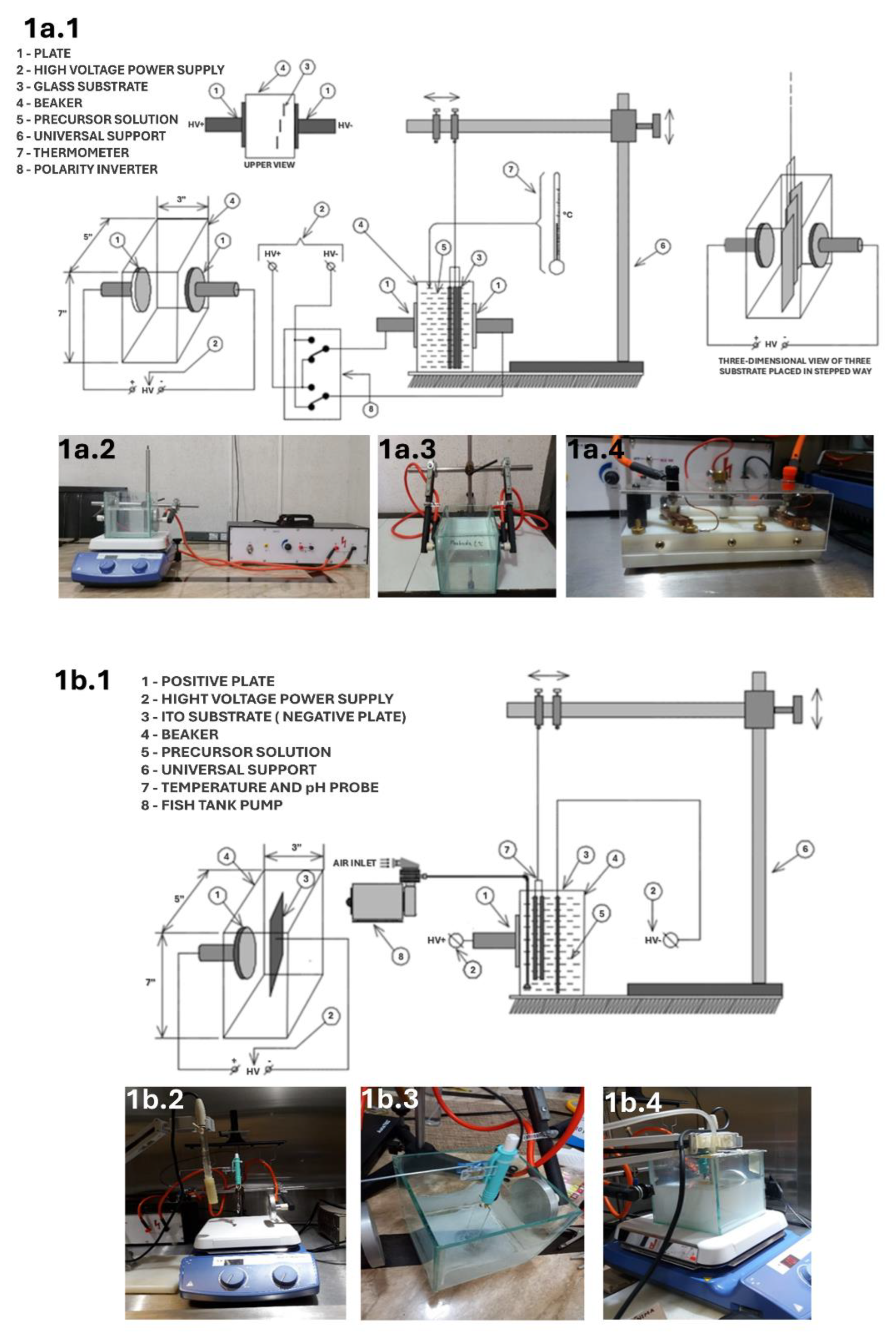
Figure 2.
XDR patterns of all samples of the CBD-HVEF-A system.
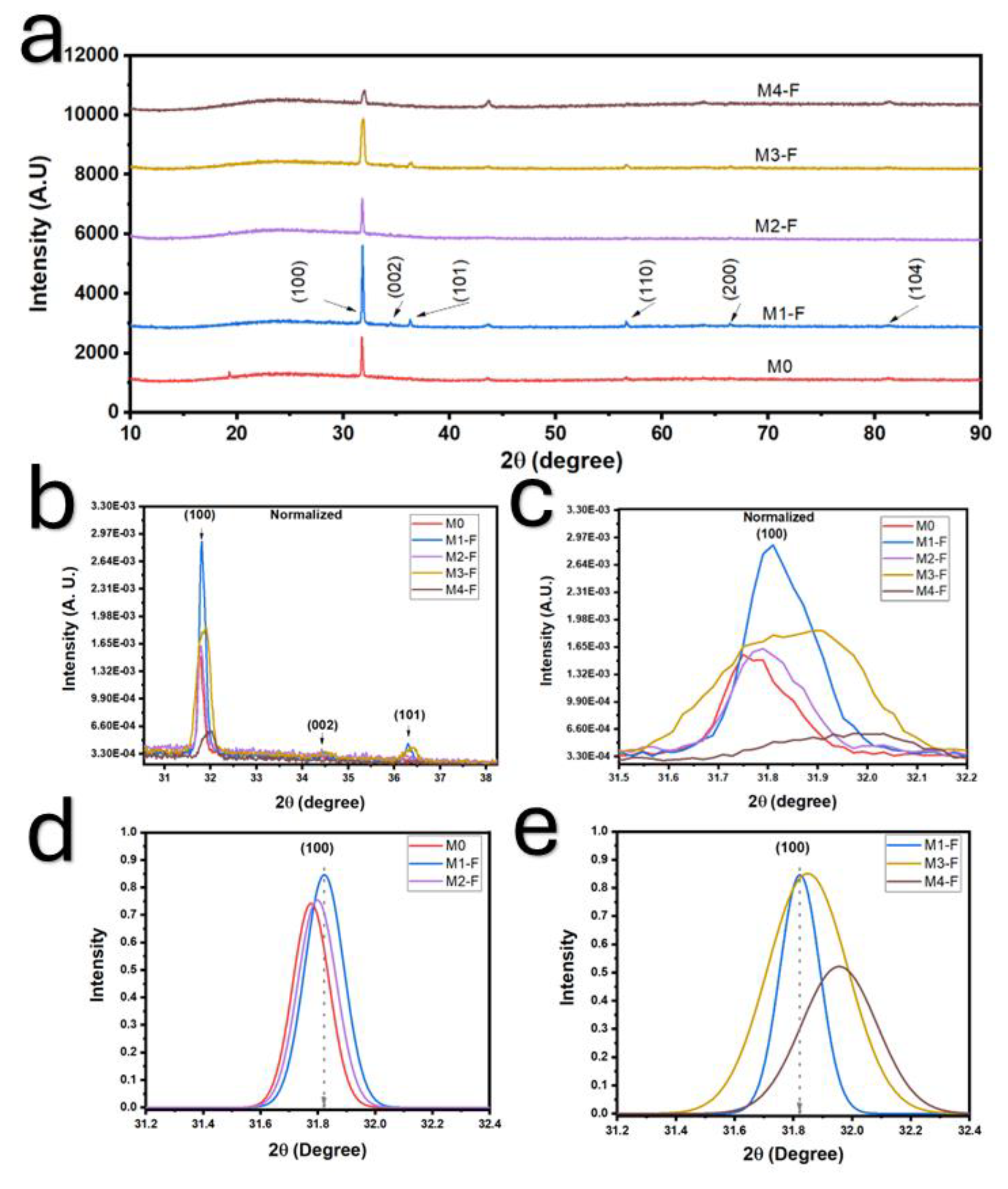
Figure 3.
ZnO micrographs of the films, as well as their corresponding size distribution functions for the ZnO rods comprising each sample. obtained using CBD-HVEF-A. The film synthesis parameters are shown in Table 1. Each micrograph has the percentage of the substrate area covered by ZnO inserted in the upper right corner.
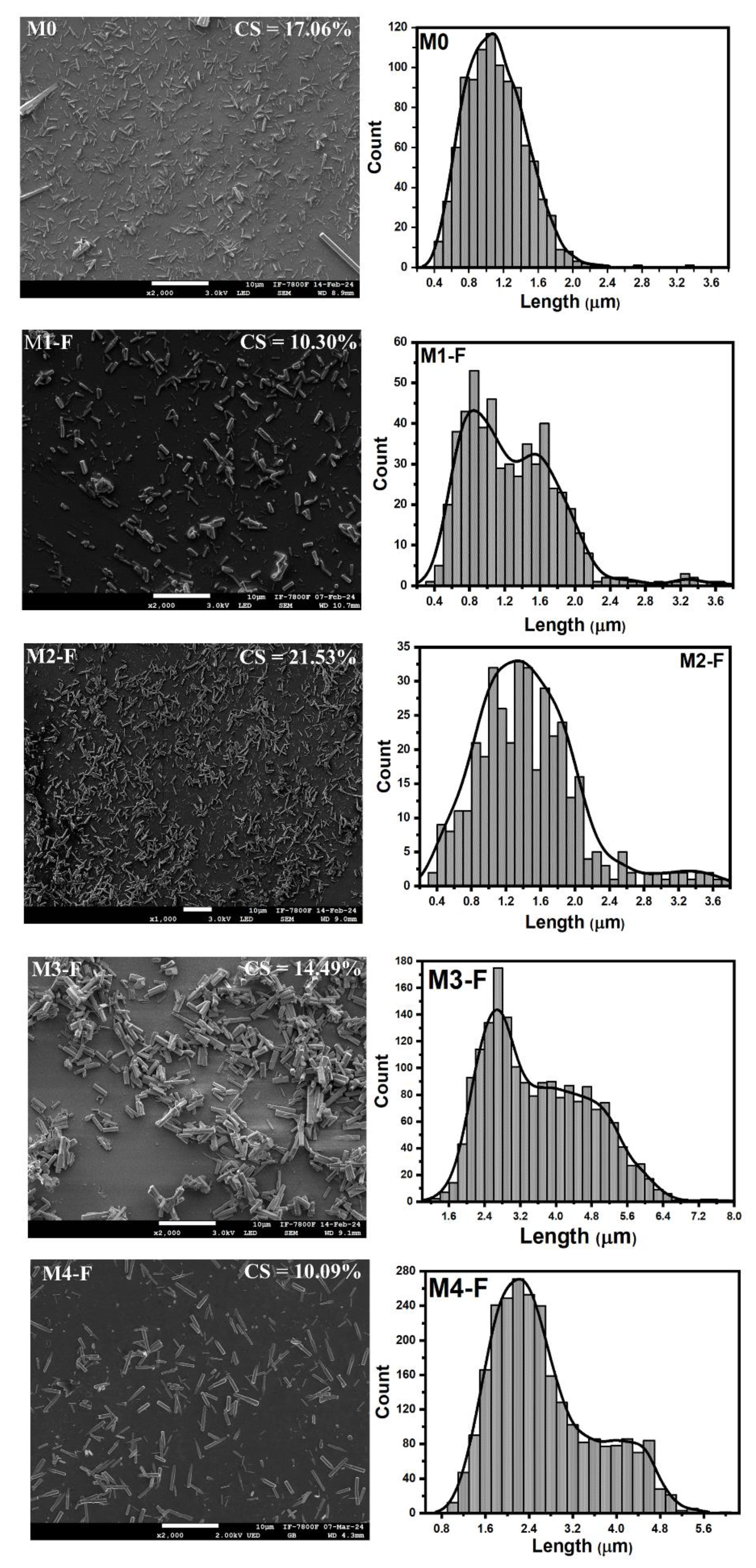
Figure 4.
Cumulative curves of the length of the ZnO bars for samples synthesized using the CBD-HVEF-A system. The inset table shows the slope values for each sample.
Figure 4.
Cumulative curves of the length of the ZnO bars for samples synthesized using the CBD-HVEF-A system. The inset table shows the slope values for each sample.
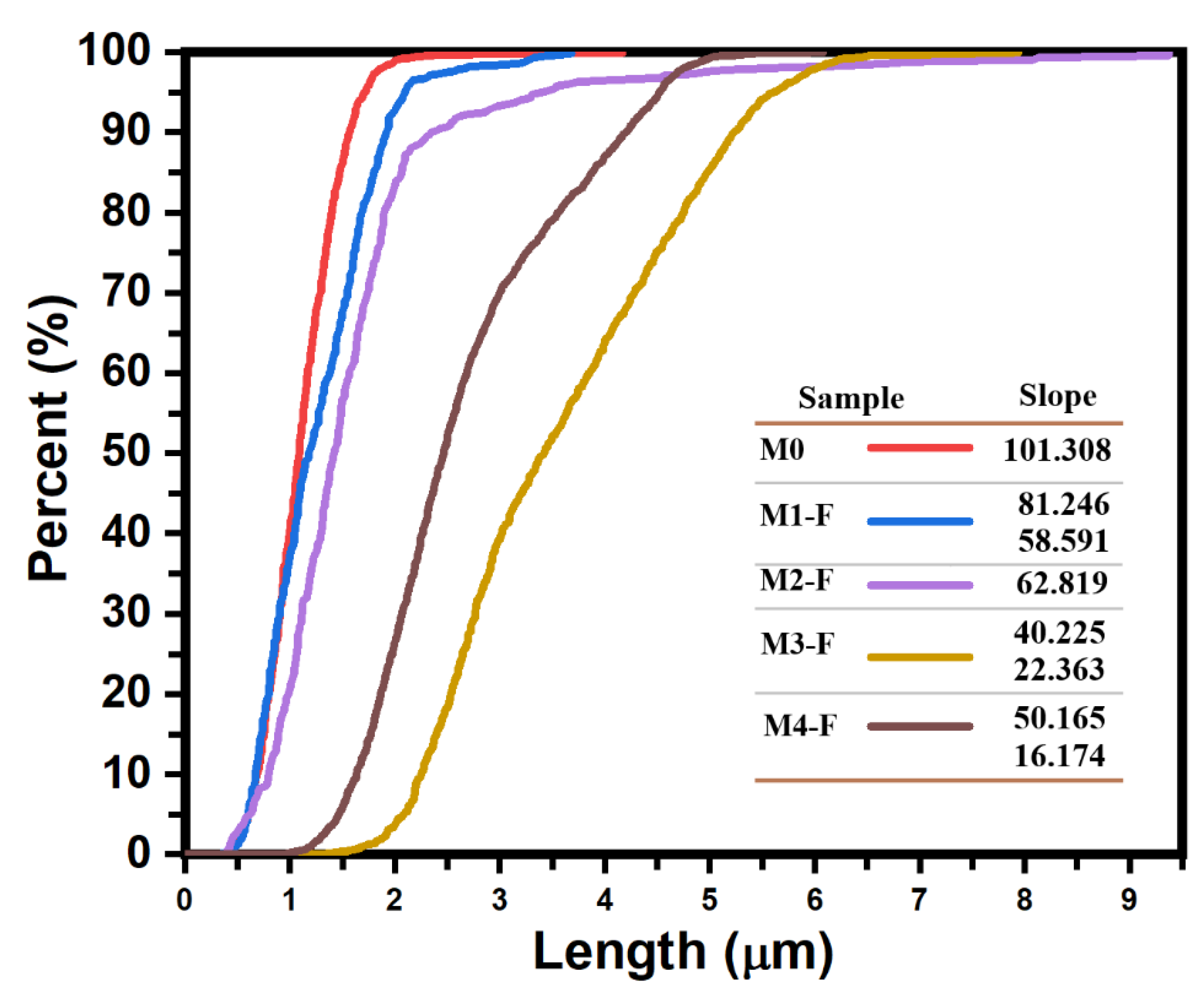
Figure 5.
Absorbance spectra for samples synthesized using the CBD-HVEF-A system. The inserted image and table correspond to their transmittance spectra and intraband absorption values, respectively.
Figure 5.
Absorbance spectra for samples synthesized using the CBD-HVEF-A system. The inserted image and table correspond to their transmittance spectra and intraband absorption values, respectively.
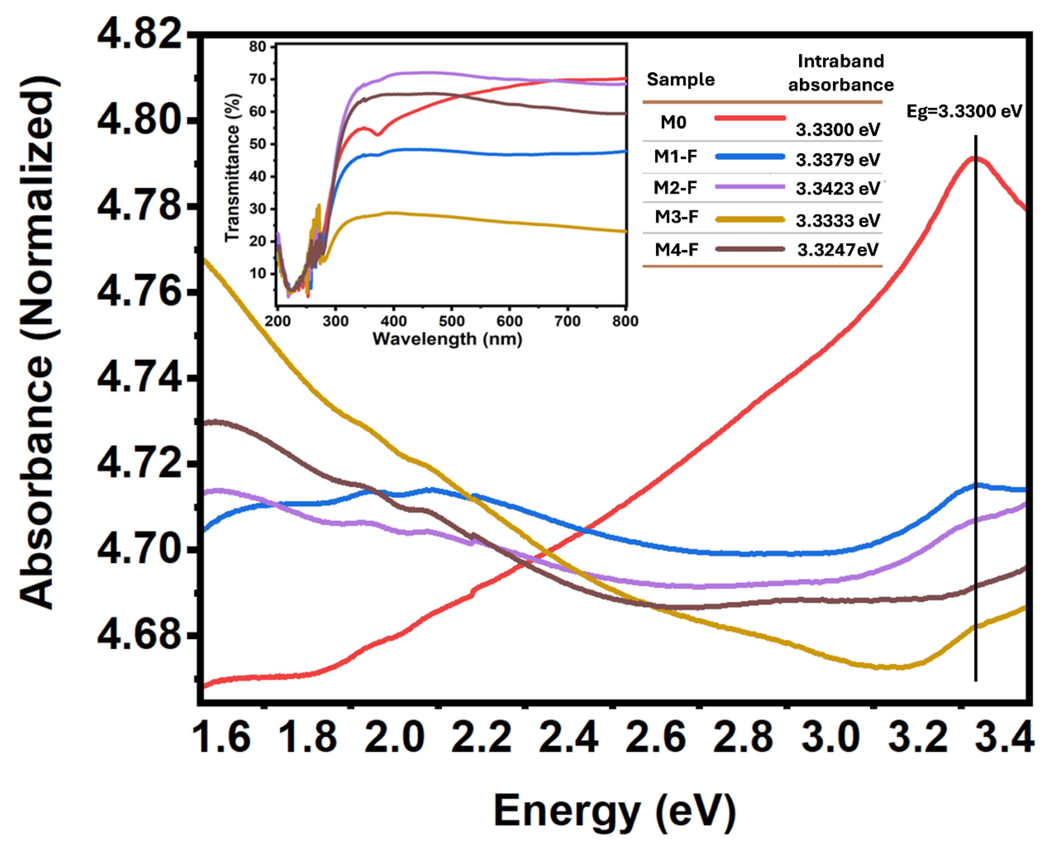
Figure 6.
ZnO micrographs of the films obtained using CBD-HVEF-B. The film synthesis parameters are shown in Table 2. Each micrograph has the percentage of the substrate area covered by ZnO inserted in the upper right corner.
Figure 6.
ZnO micrographs of the films obtained using CBD-HVEF-B. The film synthesis parameters are shown in Table 2. Each micrograph has the percentage of the substrate area covered by ZnO inserted in the upper right corner.
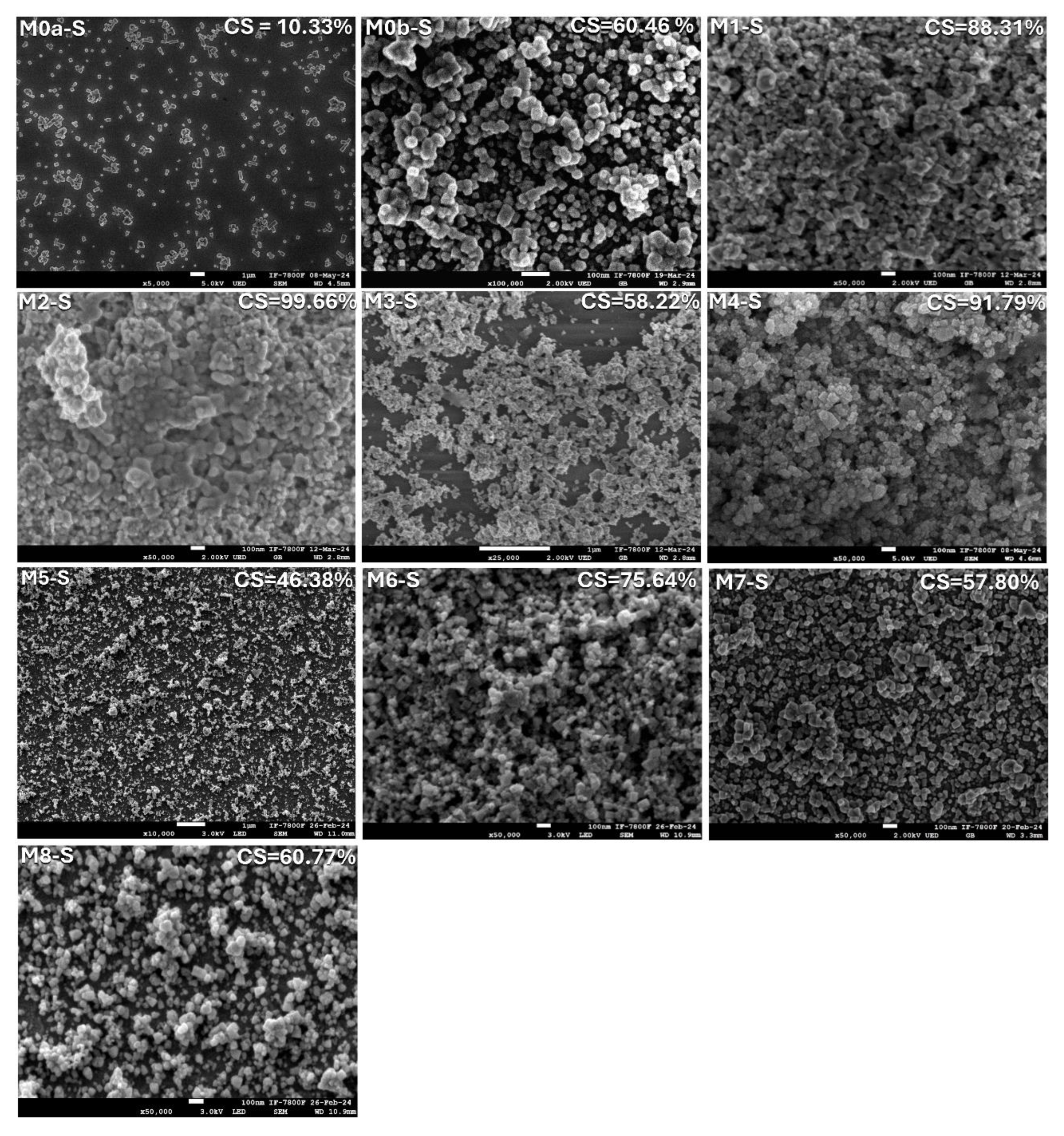
Figure 7.
Particle size histograms of the films obtained with CBD-HVEF-B. Each histogram has its corresponding cumulative percentage curve inserted in the upper right corner. The table shows the descriptive statistics for the simples.
Figure 7.
Particle size histograms of the films obtained with CBD-HVEF-B. Each histogram has its corresponding cumulative percentage curve inserted in the upper right corner. The table shows the descriptive statistics for the simples.
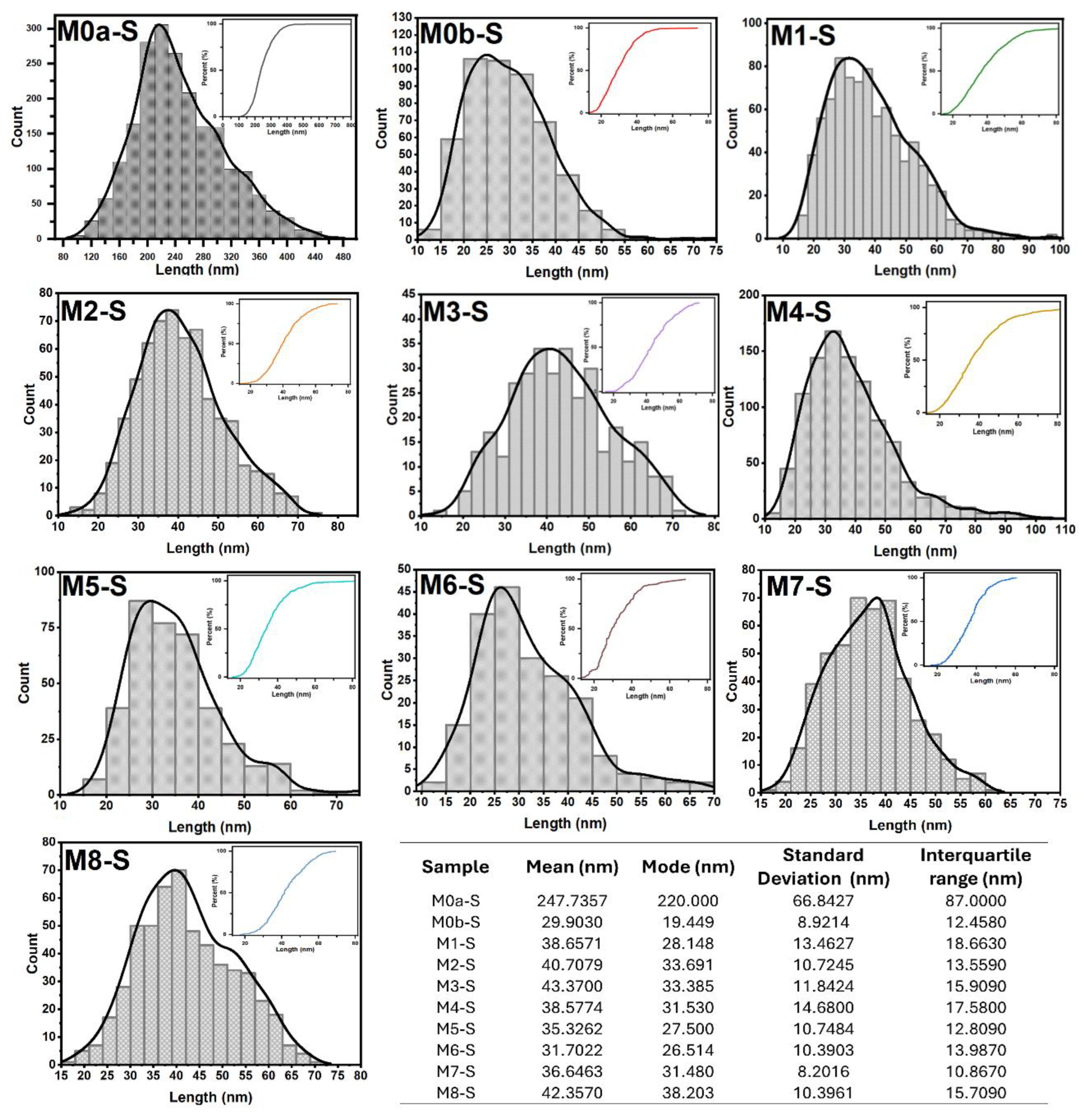
Figure 8.
Comparative analysis between the length and size dispersion of the particles that make up the samples, by comparing their corresponding cumulative curves. a) Effect of electric field; b) Effect of electric field intensity; c) Effect of both: stirring with filtered air and electric field intensity; d, e and f) Effect of stirring with filtered air; g and f) Effect of pH change.
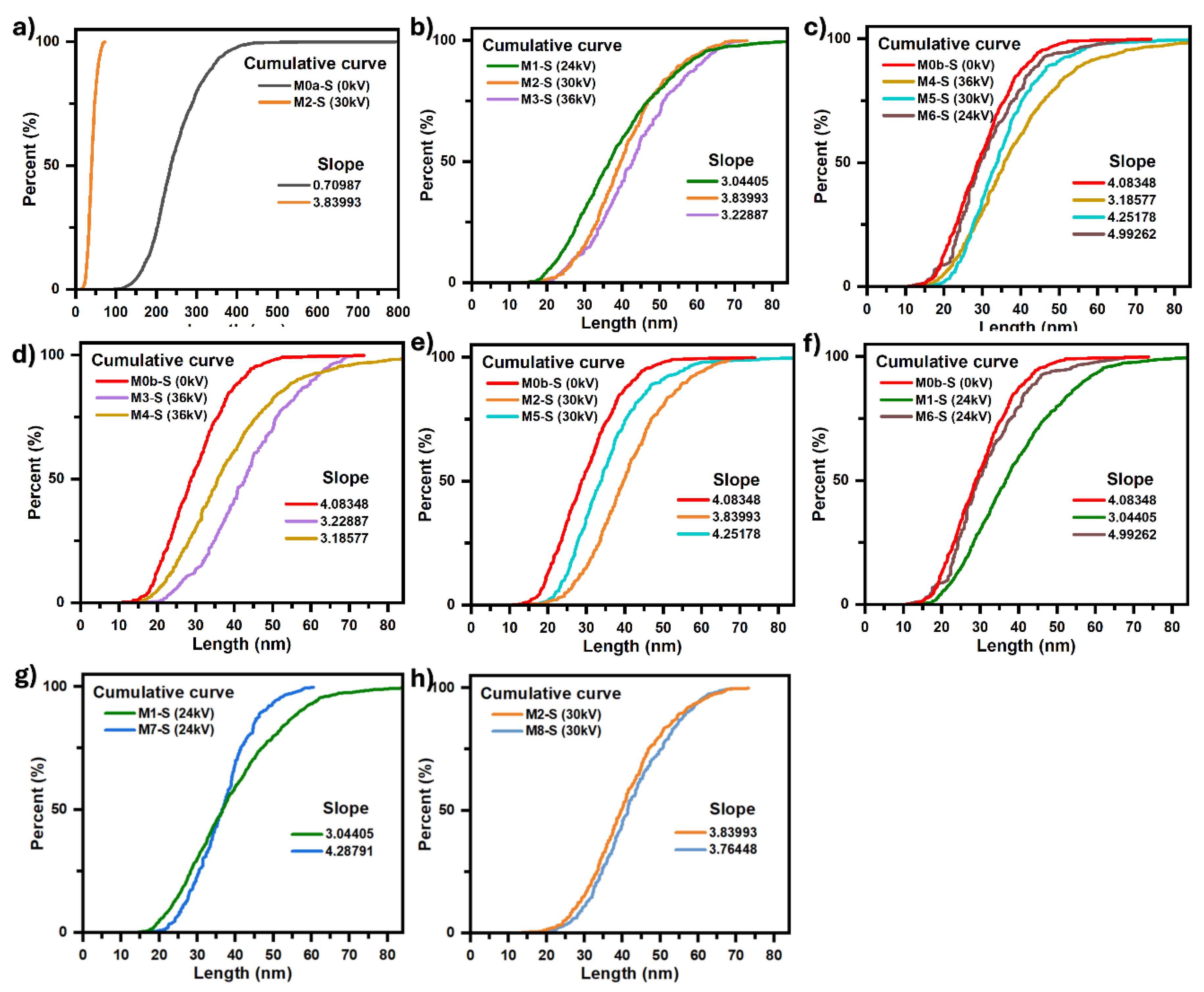
Figure 9.
Temperature curves of the precursor solution during the synthesis process. The curves were grouped according to each comparative analysis in Figure 8.
Figure 9.
Temperature curves of the precursor solution during the synthesis process. The curves were grouped according to each comparative analysis in Figure 8.
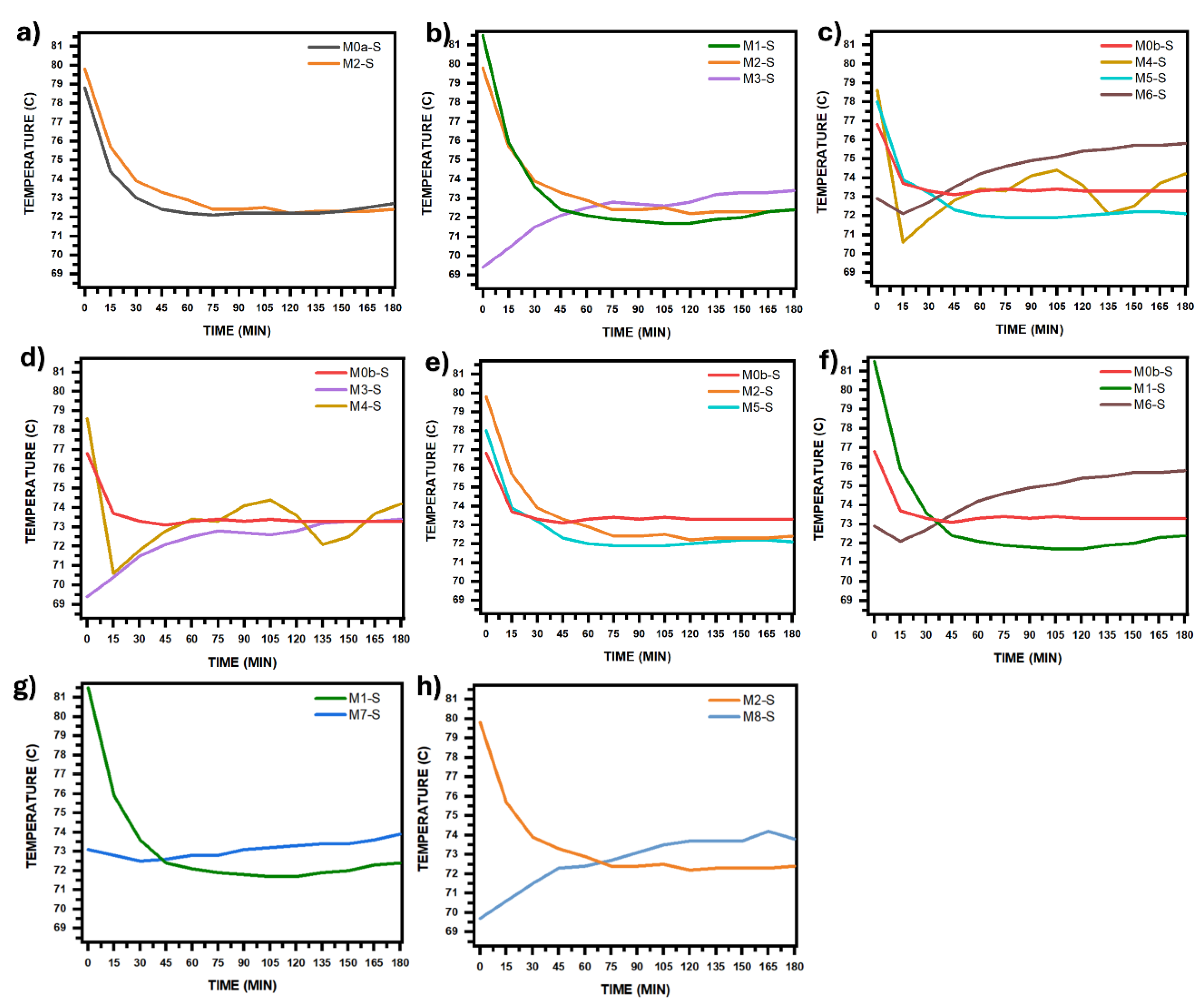
Figure 10.
pH curves of the precursor solution during the synthesis process. The curves were grouped according to each comparative analysis in Figure 8.
Figure 10.
pH curves of the precursor solution during the synthesis process. The curves were grouped according to each comparative analysis in Figure 8.
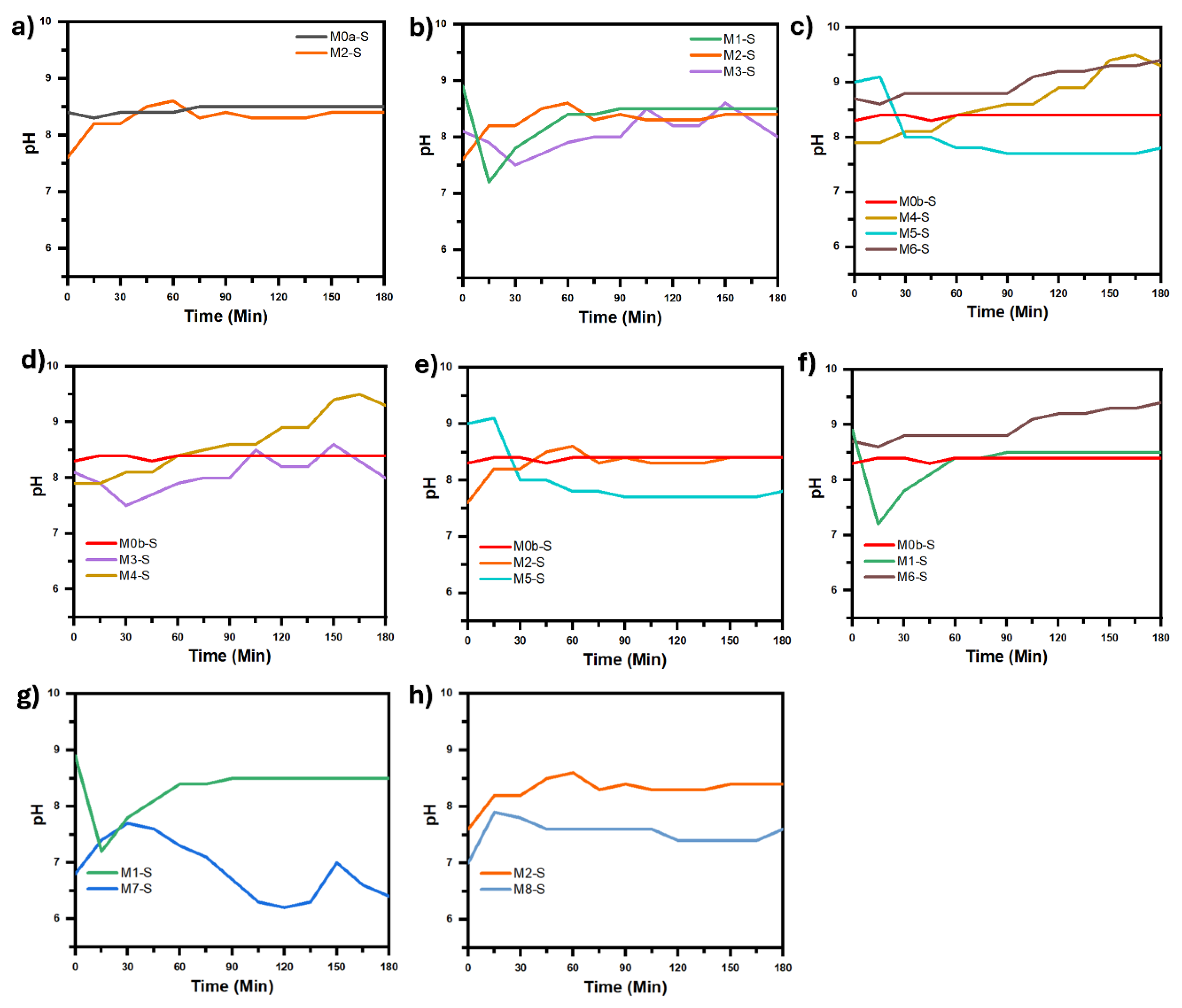

Table 1.
Samples synthesized using CBD-HVEF-A as a function of the voltage applied between parallel metal plates to produce an electric field and the period in which the electrical polarity of the plates is reversed. The asterisk “*” signifies that polarity inversion was not done for these samples.
Table 1.
Samples synthesized using CBD-HVEF-A as a function of the voltage applied between parallel metal plates to produce an electric field and the period in which the electrical polarity of the plates is reversed. The asterisk “*” signifies that polarity inversion was not done for these samples.
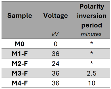 |
Table 2.
Samples synthesized using CBD-HVEF-B as a function of the voltage applied between the ITO substrate immersed vertically in the precursor solution and the metal plate placed parallel to it on the outer vertical surface of the container to generate an electric field between them. The last column indicates whether the samples were synthesized by injecting air into the precursor solution during the synthesis process to create bubbles in it, in addition to an electric field.
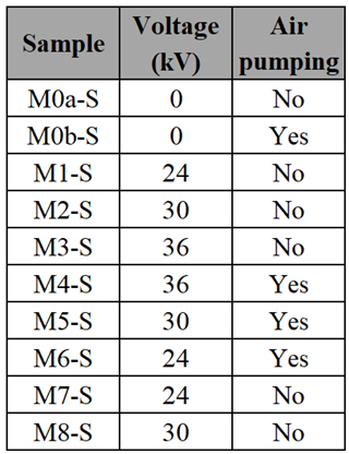 |
Table 3.
Interplanar distance and grain size values for all samples, considering peak (100).
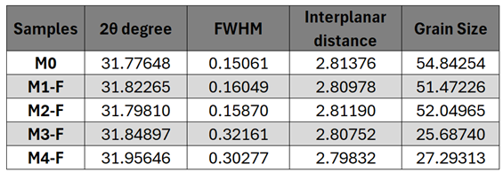 |
Table 4.
Descriptive statistics of the distribution functions presented in Figure 3.
Table 4.
Descriptive statistics of the distribution functions presented in Figure 3.
 |
Disclaimer/Publisher’s Note: The statements, opinions and data contained in all publications are solely those of the individual author(s) and contributor(s) and not of MDPI and/or the editor(s). MDPI and/or the editor(s) disclaim responsibility for any injury to people or property resulting from any ideas, methods, instructions or products referred to in the content. |
© 2025 by the authors. Licensee MDPI, Basel, Switzerland. This article is an open access article distributed under the terms and conditions of the Creative Commons Attribution (CC BY) license (http://creativecommons.org/licenses/by/4.0/).
Copyright: This open access article is published under a Creative Commons CC BY 4.0 license, which permit the free download, distribution, and reuse, provided that the author and preprint are cited in any reuse.


