Submitted:
04 June 2025
Posted:
05 June 2025
Read the latest preprint version here
Abstract
This work presents an ultra-compact and feasible three-way power splitter design tailored for photonic integrated circuits, achieved through topological optimization employing a custom-developed genetic algorithm. Miniaturization of waveguide turns, which are critical part of all optical systems, directly contributes to compactness of the system. The considered method maintains good transmission uniformity and minimal mode mismatch while allowing global shape reconfiguration within a confined footprint of 1.56 λ² ( λ=1550 nm) unlike conventional curve-based methods. The optimized structure demonstrates a 93% output similarity validated through time-domain simulations. These remarkable performance outcomes can be implemented on both communication wavelength and microwave applications.
Keywords:
Power Splitter
; Photonic Integrated Circuits
; Artificial Intelligence
; Genetic Algorithm
1. Introduction
Studies performed over the recent years show a notable variation and creativeness in the designs of T-junctions and in general N-way power splitters for small optical devices. Particularly, ultra-compact Y- and T-junction dividers, optimized utilizing algorithms assisted by artificial intelligence on the LNOI (lithium niobate on insulator) platform by Xu et al. [1], have attracted great interest. Long et al. [2] have created a low-loss and small dual-mode splitter combining Y-junction, multimode interferometer, and routing coupler. Similarly, Wahsheh [3] offers a plasmonic power divider defined by a broadband and 3 dB output within a metal-dielectric-metal structure. Concurrently, Geerthana et al. [4] showed that high terahertz applications of T-, Y-, and E-junction designs made of 2D photonic crystals can attain great efficiency. While Su et al. [5] created an ultra-wideband and adjustable splitter incorporating a SB2Se3 doped Y-junction, Makwana and Chaplain [6] produced configurable three-way energy dividers using topological structures. The geometric design of the optical medium enables the adiabatic transformation of the three-way splitter into a wave steerer around sharp angle bends.
All of the above-mentioned researches provide major developments in the field of small optical power dividers, providing methods that optimize space use, lower losses, and improve manufacture within modern photonic systems. And, fundamental part of dividers require beam steering which is a more specific topic in photonic applications. In this manner, multimode waveguide (MMW) bends allow flexible and tightly packed configurations within mode-division multiplexing (MDM) based photonic integrated circuits (PICs). Achieving ultra-compact designs without compromising performance remains a major challenge [7,8,9,10,11]. High-order modes suffer increased radiation and scattering losses when the bending radius decreases, ascribed to reduced optical confinement and a stronger interaction with waveguide flaws [12,13,14]. Sharp bends especially show the impacts since a significant mode mismatch between straight and curved sections causes increased insertion loss (IL) and inter-mode crosstalk (CT) [15,16,17]. (MDM) has recently become a powerful method for significantly increasing the data transmission capacity of optical communication networks. Multiple orthogonal modes help to transport different data streams inside a single multimode waveguide, therefore improving bandwidth efficiency and integration density. Apart from MMWs, single mode waveguides (SMWs) suffer from radiation losses even more especially through sharp waveguide bends. This type of loss increases if the refracitve index of the waveguide is relatively low.
Several approaches have been proposed to address these issues on both MMWs and SMWs. Oner et al. proposed graded index distribution as a key factor on beam bending [18]. Notably, subwavelength grating (SWG) [19,20] and transformation optics (TO) [16,21] methods possess the ability to improve mode matching, although they often require complex fabrication procedures. These techniques may show restrictions in their capacity to generate ultra-compact design, otherwise the optimization of trajectories using Bezier [22] or Euler [23] curves presents solutions more fit for production. Dual Bezier curve-based MWBs obtained using particle swarm optimization (PSO) maintains low IL and CT by allowing arbitrary-angle bends and numerous transverse electric (TE) modes while still accommodating. These techniques show the possibility for both compactness and great transmission quality; yet, face limitations in handling higher-order mode stability at ultra-small radii. While inverse design approaches using free-form curves [24,25] or topology optimization [26,27] show great compactness and performance gains, they may need computationally intensive processes and yield structures with insufficient fabrication tolerance.
Regarding all of the improvements on beam bending and power splitting methodology, the authors have found topological optimization by artificial intelligence based algorithms as a preferable technique on ultra-compact optical device designs. In addition, larger space requirement of a three-way splitter enhances the challenge factor of the compactness problem. Device sizes beside equal power transmission are considered as a parameter of success criteria of topology optimization within this scope. The organization of this work is as follows: Section 2 clarifies the problem and suggested design approach. Section 3 covers the simulation setup, tackles performance evaluation and present the consequent comparison. Finally, Section 4 offers final remarks.
2. Materials and Methods
2.1. Three-Way Power Splitter
A standard N-way power splitter consists of an input waveguide and N-output waveguides which is an essential passive part of many optical communication systems, especially photonic integrated circuits (PICs). Its main job is to equally split an incoming optical signal into N-output pathways. In order to facilitate signal distribution, monitoring, and processing across many optical systems, this division is essential. The optical devices that splitters widely used are input power distributors, passive optical networks, optical switches / routers, optical coupling input and output interfaces and many other subsystems.
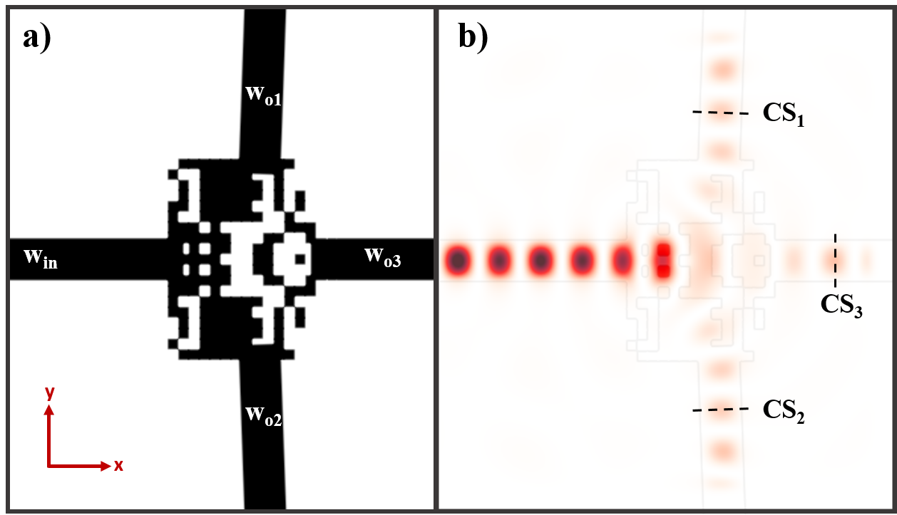
Just as electronic circuit sizes become smaller by time, optical circuits also experience the same trend. Therefore, a fundamental problem of current PIC technology lies beneath compactness limits. In this manner, three-way power splitters dramatically suffer from a trade-off between splitter performance and device size. Let us consider a standard device given by Figure 1. In such a design, the determining factor in terms of size is the radius of curvature of the output waveguides, namely . Even if this radius is chosen as ( is operating wavelength in vacuum), the ratio between H-field intensities of and is over 7.72. This significant difference in output power values directly reveals the need for a specific design in the joint area.
A conventional method utilized in the literature aims to optimize waveguide bends by continuous structures. However, as mentioned in the Introduction Section, these bends mostly can be written in terms of analytical functions. Nevertheless, random topologies generated by artificial intelligence based designs cover the analytically described bends. In this optimization process, randomness may be introduced by reshaping the topology of the turning area. When only a single material is introduced into the design, and the junction area is fixed to and the resolution of topology to then different designs are possible to generate. Herein, and scale the device size along x and y directions, respectively while n does the same inversely for resolution. As a result, an optimization method is inevitable to achieve a satisfactory performance within a compact splitter.
As mentioned in the Introduction, topological optimizations among the optical device design approaches enable miniaturized subsystems compromising fabrication tolerances. This disadvantage can be overcome by putting constraints on the parameter n in terms of feasibility. In this study, we hold in order not to encounter this challenge. Topological reshapes usually generate designs such that multiple extremum points arise as performance which is directly related to the success criteria. In this manner, genetic algorithm (GA) provides remarkably adequate designs since one of its primary advantages is being able to find the global optimum. This superiority has led the optimization methods to be based mostly on GA. Main steps of the algorithm are briefly given in the next Section.
2.2. Genetic Algorithm
A special code for the genetic algorithm was developed [28] by the authors and this code was integrated with MEEP [29] which is based on finite-difference time-domain methodology. Below is an outline of the proposed algorithm:
I) An initial population is created totally randomly within the geometric constraints of the design. Both number of candidates and maximum number of generations are determined to be 100.
II) When each cycle is completed, the performance values (output waveguide transmitted powers) of the parameters of the solution candidates are computed.
III) The next step is aimed at determining the selection criteria and subsequent crossover process. One of the standard methods, the “random gene mixing” method, is used. In addition to this method, the probability of a successful design to transfer parameters to the next generation is increased proportionally with respect to its performance value. The next generation is created from these new and randomly selected parameters, preserving the population size. In each iteration, each parameter transfer is given a 2% chance of mutation. This eliminates the dependence of the output design on only the first generation parameters.
IV) The algorithm automatically terminates itself when it reaches the target number of generations or the target success.
3. Results and Discussion
The data obtained by implementing the methodology given in Subsection 3.2 is represented and discussed below. Figure 2 shows the results of the algorithm. Figure 2(a) displays the results of each individual under the optimization performed. The initial population of 100 individuals was run until it reached 100 generations, again with 100 individuals in each generation. The success of the process can be seen in Figure 2(b). Here, each point gives the arithmetic mean performance values of its own generation. An average success ratio of 10% is obtained by random initial parameters and the plot tends to saturate below 60% at first within 20 generations if mutation probability doesn’t exist. However, it finally increases up to 80% by introducing mutation.
Parameters corresponding to the best result of the GA is considered for time-domain simulations. Dielectric permittivity is which is compatible with Si3N4 low-loss waveguides [30]. The resolution of topology is and scaling factors are and . Hence, total junction area is . If the operating vacuum wavelength is chosen as , then the width of all waveguides become .
Figure 3(a) shows the finalized junction geometry of three-way power splitter which is symmetrical with respect to x-axis. The waveguides and are tilted after the GA optimization to perfectly eliminate mode-misalignment. When the field energy values transmitted to the waveguides at the points taken on the CS1,2 and CS3 cross-sections are compared, their similarity is at a rate of . This value is below 7% when standard approach as given in the inset of Figure 1 with and total junction size of .
When evaluated in respect to their main functionality and design approach, this work shows the best degree of resemblance to the cited study of Ref. [1]. Particularly, the Y- and T-type splitters included in that work show . (2.60 μm × 2.60 μm) and (2.85 μm × 4.94 μm), respectively. Still, should a 90 degree T-type three-way splitter be required, such splitters call for an additional layer in the design. Usually matching the number of outputs, the demand increases in line with N for N-way splitters. Conversely, the present research reveals that one can construct a geometry very well-suited for N-way splitting configurations by generalizing the suggested design process.
From the perspective of physical dimensions, our solution stands out mostly for its ability to achieve efficient beam steering around steep bends, even in low refractive index contrast. Although Ref. [18] shows strong transmission across two different frequency bands through an analytically well-defined graded refractive index function, the structure lacks sufficient compactness. In a similar line, a recent work reported as Ref. [7] achieves high-efficiency bending across several optical modes by means of analytically determined Bezier-shaped curves. Still, the construction’s dimensions remain larger than that of desired by PIC designs. Finally, when considering all the performance parameters required for a junction region, the geometry proposed in this paper demonstrates superiority.
4. Conclusions
This research addresses reducing the size of the junction area of power splitters in photonic integrated circuits. A novel N-way splitter design technique including topology optimization via genetic algorithm code developed by authors is proposed. Our method efficiently preserves strong optical confinement through ultra-compact junction area even though light confinement and beam steering by relatively low refractive indices is challenging. Nevertheless, the optimized geometry reduces both radiation and scattering losses by means of merging the smooth and controllable properties with global shape modification.
An input power transmitted by transverse electric fundamental mode is divided into 90 degree seperated almost equal three output parts within ultra-compact structure smaller than 1.56 . The similarity of output waves is managed to increase more than 13 times compared to a standard divider with even larger geometry. These results can directly be implemented on real applications such as optical chip input power dividers that include Si3N4 waveguides on SiO2 substrate. In addition, scalability of Maxwell’s Equations enable the structure to be operable within microwave regime. In this case, experimental stuides can be carried out by low-loss and easily accessible commercial-off-the-shelf materials (i.e., TPU, Alumina, etc.) with the same permittivity (). This approach provides a strong, fabrication-friendly solution for upcoming high-density power-divider systems.
Author Contributions
The following statements should be used “Conceptualization, ALP and ONER.; methodology, ALP and ONER.; software, ONER; validation, ALP and ONER; formal analysis, ALP and ONER; investigation, ALP; resources, ALP and ONER; writing—original draft preparation, ALP and ONER.; writing—review and editing, ALP and ONER; visualization, ALP and ONER. All authors have read and agreed to the published version of the manuscript.”
Funding
This research received no external funding.
Institutional Review Board Statement
Not applicable.
Informed Consent Statement
Not applicable.
Data Availability Statement
The raw data supporting the conclusions of this article will be made available by the author upon request.
Conflicts of Interest
The authors declare no conflicts of interest.
References
- Xu, Q.; Liu, J.M.; Zhang, D.L.; Hua, P.R. Ultra-Compact Lithium Niobate Power Splitters Designed by an Intelligent Algorithm. Optics & Laser Technology 2023, 160, 109057. [Google Scholar] [CrossRef]
- Long, J.; Jia, H.; Zhang, J.; Chen, C. Low-Loss and Compact, Dual-Mode, 3-dB Power Splitter Combining a Directional Coupler, a Multimode Interferometer, and a Y-Junction. Appl. Opt. 2024, 63, 2030–2035. [Google Scholar] [CrossRef] [PubMed]
- Wahsheh, R.A. Ultra-Compact Broadband 3-dB Metal–Dielectric–Metal Plasmonic Power Splitter. J. Mod. Opt. 2021, 68, 153–160. [Google Scholar] [CrossRef]
- Geerthana, S.; Sridarshini, T.; Balaji, V.R.; Sitharthan, R.; Madurakavi, K.; Thirumurugan, A.; Dhanabalan, S.S. Ultra Compact 2D-PhC Based Sharp Bend Splitters for Terahertz Applications. Opt. Quantum Electron. 2023, 55, 778. [Google Scholar] [CrossRef]
- Su, Y.; Zhang, Y.; Zhou, X.; Liu, D.; Zhang, M. Ultra Broadband Tunable Power Splitter Based on Sb2Se3-Assisted Y-Junction. J. Lightwave Technol. 2023, 42, 2817–2822. [Google Scholar] [CrossRef]
- Makwana, M.P.; Chaplain, G. Tunable Three-Way Topological Energy-Splitter. Sci. Rep. 2019, 9, 18939. [Google Scholar] [CrossRef]
- Zhou, S.; Yu, X.; Yuan, Q.; Sui, X. Ultra-compact multimode waveguide bend based on a central width controllable dual Bezier structure. Opt. Lett. 2025, 50, 1985–1988. [Google Scholar] [CrossRef]
- Lan, Y.; Liu, S.; Cheng, C.; Chen, X.; Fu, X.; Yang, L. Ultra-compact multimode waveguide bends with arbitrary bending angles. Opt. Express 2025, 33, 13133–13144. [Google Scholar] [CrossRef]
- Liu, S.; Niu, J.; Huo, Y.; Cheng, C.; Fu, X.; Yang, L. Ultra-compact and fabrication-tolerant multimode photonic jumpers based on dual Bezier curves. Opt. Lett. 2024, 49, 3352–3355. [Google Scholar] [CrossRef]
- Liao, J.; Tian, Y.; Yang, Z.; Xu, H.; Dai, T.; Zhang, X.; Kang, Z. Broadband and compact silicon multimode waveguide bends based on hybrid shape optimization. J. Lightwave Technol. 2024, 42, 4882–4891. [Google Scholar] [CrossRef]
- Cheng, C.; Yang, S.; Liu, W.; Liu, S.; Huo, Y.; Fu, X.; Yang, L. Ultra-compact inverse designed multimode waveguide bend based on levelset method. IEEE Photonics Technol. Lett. 2024, 36, 571–574. [Google Scholar] [CrossRef]
- Sun, S.; Yang, Z.; Wang, J.; Zhang, R.; Zhang, F.; Zhu, N.; Li, Z. Ultra-sharp silicon multimode waveguide bends based on double free-form curves. Photonics Res. 2022, 10, 1484–1490. [Google Scholar] [CrossRef]
- Bogaerts, W.; Chrostowski, L. Silicon photonics circuit design: methods, tools and challenges. Laser Photonics Rev. 2018, 12, 1700237. [Google Scholar] [CrossRef]
- Bogaerts, W.; De Heyn, P.; Van Vaerenbergh, T.; De Vos, K.; Kumar Selvaraja, S.; Claes, T.; Baets, R. Silicon microring resonators. Laser Photonics Rev. 2012, 6, 47–73. [Google Scholar] [CrossRef]
- Li, F.; Ding, F.; Wu, R.; Liu, Y.; Xu, K. Compact four-mode silicon multimode bends with a 500 nm bandwidth. In Proceedings of the 2023 Opto-Electronics and Communications Conference (OECC), Shanghai, China, 2–6 July 2023; pp. 1–3. [Google Scholar] [CrossRef]
- Li, S.; Cai, L.; Gao, D.; Dong, J.; Hou, J.; Yang, C.; Chen, S.; Zhang, X. Compact and broadband multimode waveguide bend by shape-optimizing with transformation optics. Photonics Res. 2020, 8, 1843–1849. [Google Scholar] [CrossRef]
- Liu, Y.; Xu, K.; Wang, S. ; Others. Arbitrarily routed mode-division multiplexed photonic circuits for dense integration. Nat. Commun. 2019, 10, 3263. [Google Scholar] [CrossRef]
- Oner, B.B.; Turduev, M.; Kurt, H. High-Efficiency Beam Bending Using Graded Photonic Crystals. Opt. Lett. 2013, 38, 1688–1690. [Google Scholar] [CrossRef]
- Wu, H.; Li, C.; Song, L.; Tsang, H.K.; Bowers, J.E.; Dai, D. Ultra-sharp multimode waveguide bends with subwavelength gratings. Laser Photonics Rev. 2019, 13, 1800119. [Google Scholar] [CrossRef]
- Xu, H.; Shi, Y. Ultra-sharp multi-mode waveguide bending assisted with metamaterial-based mode converters. Laser Photonics Rev. 2018, 12, 1700240. [Google Scholar] [CrossRef]
- Gabrielli, L.H.; Liu, D.; Johnson, S.G.; Lipson, M. On-chip transformation optics for multimode waveguide bends. Nat. Commun. 2012, 3, 1217. [Google Scholar] [CrossRef]
- Jiang, X.; Wu, H.; Dai, D. Ultra-compact multimode waveguide bend based on optimized shape. Opt. Express 2018, 26, 17680. [Google Scholar] [CrossRef] [PubMed]
- Wu, X.; Zhou, W.; Huang, D.; Zhang, Z.; Wang, Y.; Bowers, J.; Tsang, H.K. Low crosstalk bent multimode waveguide for on-chip mode-division multiplexing interconnects. In Proceedings of the Conference on Lasers and Electro-Optics (CLEO), Optica Publishing Group, Online, 2018. Paper JW2A.66. [Google Scholar] [CrossRef]
- Sun, S.; Dong, P.; Zhang, F.; Wang, J.; Zhu, N.; Shi, Y. Inverse design of ultra-compact multimode waveguide bends based on the free-form curves. Laser Photonics Rev. 2021, 15, 2100162. [Google Scholar] [CrossRef]
- Chen, Y.; Qiu, J.; Dong, Z.; Wang, L.; Liu, Y.; Guo, H.; Wu, J. Inverse design of free-form devices with fabrication-friendly topologies based on structure transformation. J. Lightwave Technol. 2023, 41, 4762–4776, https://opg.optica.org/jlt/abstract.cfm?URI=jlt-41-14-4762. [Google Scholar] [CrossRef]
- Iguchi, A.; Tsuji, Y.; Yasui, T.; Hirayama, K. Topology optimal design for optical waveguides using time domain beam propagation method. IEICE Electron. Express 2018, 15, 20180417. [Google Scholar] [CrossRef]
- Tsuji, Y. ; Others. Design of optical circuit devices based on topology optimization. IEEE Photonics Technol. Lett. 2006, 18, 850. [Google Scholar] [CrossRef]
- The MathWorks, Inc. MATLAB R2023b; The MathWorks, Inc.: Natick, MA, USA, 2023. [Google Scholar]
- Oskooi, A.F.; Roundy, D.; Ibanescu, M.; Bermel, P.; Joannopoulos, J.D.; Johnson, S.G. MEEP: A flexible free-software package for electromagnetic simulations by the FDTD method. Comput. Phys. Commun. 2010, 181, 687–702. [Google Scholar] [CrossRef]
- Bauters, J.; Heck, M.; John, D.; Dai, D.; Tien, M.; Barton, J.; Leinse, A.; Heideman, R.; Blumenthal, D.; Bowers, J. Ultra-low-loss high-aspect-ratio Si3N₄ waveguides. Opt. Express 2011, 19, 3163–3174. [Google Scholar] [CrossRef]
Figure 1.
A standard three-way beam splitter. Waveguide width values of the all input and output waveguides are kept same at with dielectric permittivity values of . Inset shows energy distribution when .
Figure 1.
A standard three-way beam splitter. Waveguide width values of the all input and output waveguides are kept same at with dielectric permittivity values of . Inset shows energy distribution when .
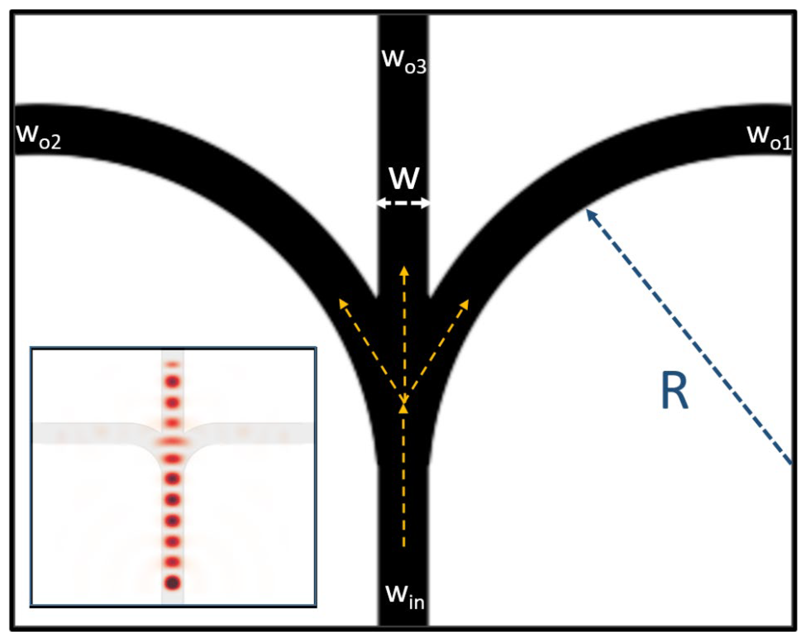
Figure 2.
(a) The performance of each solution candidate across 100 generations is exhibited in a normalized format. (b) The average performance of each generation is plotted in a normalized fashion. Both normalizations are taken relative to the best-performing solution candidate of all.
Figure 2.
(a) The performance of each solution candidate across 100 generations is exhibited in a normalized format. (b) The average performance of each generation is plotted in a normalized fashion. Both normalizations are taken relative to the best-performing solution candidate of all.

Figure 3.
(a) The resulting geometry of the best solution is shown. (b) The time-averaged field energy density () under steady-state condition.
Figure 3.
(a) The resulting geometry of the best solution is shown. (b) The time-averaged field energy density () under steady-state condition.

Disclaimer/Publisher’s Note: The statements, opinions and data contained in all publications are solely those of the individual author(s) and contributor(s) and not of MDPI and/or the editor(s). MDPI and/or the editor(s) disclaim responsibility for any injury to people or property resulting from any ideas, methods, instructions or products referred to in the content. |
© 2025 by the authors. Licensee MDPI, Basel, Switzerland. This article is an open access article distributed under the terms and conditions of the Creative Commons Attribution (CC BY) license (https://creativecommons.org/licenses/by/4.0/).
Copyright: This open access article is published under a Creative Commons CC BY 4.0 license, which permit the free download, distribution, and reuse, provided that the author and preprint are cited in any reuse.


