Submitted:
03 June 2025
Posted:
03 June 2025
You are already at the latest version
Abstract
This work presents a systematic first-principles investigation of the electronic structure and bandgap modulation in Cu2Ni(Sn,Ge,Si)Se4 kesterites using density functional theory (DFT). Geometry optimizations were performed using the SCAN functional, followed by electronic structure calculations with the hybrid HSE06 functional to ensure high accuracy. Convergence tests were carried out to determine the optimal values of plane-wave cutoff energy (450 eV) and k-point mesh (4×4×2), ensuring precise energy calculations while minimizing computational cost. Our study reveals that the substitution of Sn with Ge and Si leads to a progressive increase in the bandgap, ranging from 0.79 eV (Sn) to 2.35 eV (Si), allowing for fine-tuning of absorption edge energies. The evaluation of the effective masses of electrons and holes relative to the free electron rest mass (m0) showed an increase from 0.25–0.35 m0 (Sn-based) to 0.38–0.50 m0 (Si-based), reflecting a reduction in band curvature near the Fermi level. Spin-polarized density of states (DOS) analysis shows a transition from weakly magnetic behavior in Cu2NiSnSe4 to a non-magnetic semiconductor character in Cu₂NiSiSe₄, highlighting the significant effect of group-IV cation substitution on the electronic and magnetic properties. These findings demonstrate that Cu2Ni(Sn,Ge,Si)Se4 kesterites, with their tunable bandgaps and transport properties, are promising candidates for next-generation thin-film solar cells. Compared to conventional CZTS-based kesterites, the incorporation of Ni and the substitution of Sn with Ge and Si not only enable magnetic and bandgap modulation but also expand their application range, making them suitable for use in photovoltaics spanning from near-infrared to visible light. The tunable band gaps and electronic structures of Cu2Ni(Sn,Ge,Si)Se4 make these materials ideal candidates not only for single-junction solar cells, but also for tandem architectures and infrared photodetectors. In particular, Cu2NiSnSe4 may serve well in IR-sensing, while Cu2NiSiSe4 is optimized for visible-light photovoltaic absorption.
Keywords:
solar cells
; kesterites
; electronic structure
; earth-abundant semiconductors
; bandgap engineering
; SCAN
; HSE06
; DFT
; photovoltaic materials
INTRODUCTION
In recent decades, kesterite-based semiconductor materials have attracted considerable attention due to their promising applications in solar energy technologies. Compounds from the Cu2ZnSn(S,Se)4 (CZTSSe) family and their derivatives represent a class of highly prospective photoabsorbers owing to their favorable combination of strong light absorption, low cost, earth-abundant constituents, and environmental friendliness [1,2]. These materials, which crystallize in the I-42m space group, exhibit high compositional tunability. Cationic (Zn, Ni, Fe) and anionic (S, Se) substitutions enable effective tailoring of their electronic and optical properties, making them especially attractive candidates for next-generation photovoltaic applications. Recent advancements in kesterite-based solar absorbers underscore the importance of composition and interface engineering for enhancing device efficiency [3,4,5,6]. Notably, innovative approaches such as heat treatment in oxygen-rich environments have been shown to suppress deep-level traps in CZTSSe, leading to certified efficiencies exceeding 11.5% [7]. Similarly, energy band alignment and defect regulation strategies have enabled air-solution-processed kesterite solar cells with remarkably low open-circuit voltage (VOC) deficits [8]. These developments highlight the critical role of defect passivation and interfacial modifications in optimizing kesterite performance.
Despite significant progress in the synthesis and characterization of kesterites, unresolved challenges persist, particularly in relation to their fabrication and practical deployment. One of the key issues is the optimization of synthesis protocols to prevent the formation of secondary phases, such as Cu2SnS3, ZnS, and Cu2Se, which can severely degrade the efficiency of solar cells [9]. Recent studies have demonstrated that solution-processed precursor strategies can significantly improve the quality of CZTSSe thin films, reducing secondary phase formation and enhancing photovoltaic performance [10]. Additionally, post-annealing treatments with Cd2+ substitution have been shown to boost device efficiencies beyond 12%, further emphasizing the importance of post-deposition processing [11]. The substitution of zinc with other elements such as nickel (Cu2NiSnS4) or iron (Cu2FeSnS4) provides additional opportunities to manipulate the structural and electronic behavior of these materials [12,13]. Such substitutions improve structural stability, modulate the band gap, and can potentially enhance solar cell performance [14,15].
Bandgap engineering remains a critical area of research in kesterite optimization. Recent investigations into selenization mechanisms under ambient air conditions have revealed pathways to achieve highly efficient kesterite absorbers with tunable bandgaps [16]. Furthermore, the introduction of alternative buffer layers, such as ZnSnN2, has been shown to improve charge transport and reduce interfacial recombination losses, leading to enhanced device performance [17]. Theoretical and experimental studies have also explored the impact of cation disorder and off-stoichiometry on the electronic structure of kesterites, revealing that controlled defect engineering can significantly influence carrier recombination and optical absorption [18,19]. For instance, potassium doping has been demonstrated as an effective strategy for grain boundary passivation and defect suppression, further improving charge collection efficiency [20].
Kesterites are direct band gap semiconductors with band gaps ranging from 1.0 to 1.5 eV, which ideally matches the requirements for single-junction solar cells. Studies of their optical behavior have demonstrated high absorption coefficients in the visible spectral range, which is particularly advantageous for thin-film solar cell applications [21]. Recent work on self-powered broadband kesterite photodetectors has highlighted their potential for weak-light detection, with ultrahigh specific detectivity achieved through tailored back-contact barriers [22]. Moreover, computational studies employing advanced density functional theory (DFT) methods, including SCAN and HSE06 functionals, have provided deep insights into the electronic and optical properties of kesterites [23,24,25]. These theoretical approaches have been instrumental in predicting novel material behaviors, such as the role of van der Waals interactions in low-dimensional hybrid perovskites [26] and the piezoelectric properties of doped III-nitride semiconductors [27].
Experimental studies of kesterites such as Cu2NiSnSe4, Cu2ZnSnSe4, Cu2FeSnSe4, Cu2NiGeSe4, and their derivatives have led to several significant breakthroughs. For example, it has been shown that kesterites incorporating nickel and germanium exhibit improved optical properties and greater structural stability compared to their zinc- and tin-based counterparts [28]. Likewise, the introduction of iron into the crystal lattice enhances the likelihood of producing materials with high infrared absorption, thereby expanding their potential applications in photocatalytic and thermoelectric devices [29]. Recent advances in solution-processed CuIn(S,Se)2 solar cells have also demonstrated the potential for high-efficiency thin-film photovoltaics, further validating the viability of earth-abundant absorbers [30].
Despite significant progress in kesterite-based solar absorbers, challenges remain in optimizing their synthesis, improving stability, and fine-tuning their electronic and optical properties for enhanced device efficiency. Specifically, while substitution of cations and anions, such as Ni and group-IV elements, has shown promise in modulating the electronic structure and band gap, the exact mechanisms behind these modifications and their full potential for improving photovoltaic performance are not yet fully understood. Additionally, the integration of alternative elements like Ge and Si into kesterites introduces further complexity, requiring deeper investigation to assess the impact on the materials' structural and electronic stability. Recent first-principles studies have explored the optoelectronic potential of novel chalcogenide compounds, providing valuable insights into bandgap tuning and defect tolerance [31,32,33,34,35,36,37,38]. Furthermore, investigations into the thermoelectric and piezoelectric properties of related materials have expanded the scope of kesterite applications beyond photovoltaics [34,35,36,37,38,39].
This work aims to systematically investigate the crystal and electronic structures of Cu2Ni(Sn,Ge,Si)Se4 kesterites using density functional theory (DFT). By analyzing structural parameters, electronic density of states, band gap values, and light absorption coefficients, the study seeks to enhance the understanding of these materials and contribute to the design of more efficient and stable photoabsorbers for next-generation thin-film photovoltaic devices.
2. MATERIALS AND METHODS
In this study, the properties of kesterite compounds from the Cu2Ni(Sn, Ge, Si)Se4 family were analyzed using density functional theory (DFT). All calculations were carried out using the Vienna Ab initio Simulation Package (VASP) [40], which is based on the projector augmented-wave (PAW) method [41]. Exchange-correlation interactions were treated using several functionals, including the generalized gradient approximation (GGA) with the PBE and PBEsol parametrizations, and the meta-GGA SCAN (Strongly Constrained and Appropriately Normed) functional [42]. The SCAN and HSE06 (Heyd-Scuseria-Ernzerhof) hybrid functional [43] were primarily used due to their superior accuracy in describing structural, electronic, and optical properties, particularly the band gap.
Prior to performing structural relaxations and optoelectronic property calculations, convergence tests were conducted using the PBE functional to determine optimal values for the plane-wave energy cutoff (ENCUT) and k-point mesh density (tested using both Monkhorst-Pack and Γ-centered schemes). The convergence criteria were based on identifying the minimum ENCUT and k-point density beyond which no significant change in total energy was observed, while further increases resulted in substantial computational cost without meaningful improvements in accuracy.
The optimized parameters obtained from these convergence tests were then employed in subsequent geometry optimization calculations using the SCAN functional. Electronic structure and optical property calculations were further refined using the hybrid HSE06 functional. The exchange-correlation energy was calculated as:
where is an adjustable parameter governing the extent of short-range interactions. Parameter α is the fraction of Hartree-Fock exchange (HF). The hybrid functional () is equivalent to PBE0 [44] for and asymptotically reaches the popular PBE for . The HSE06 hybrid functional employed a screening parameter ω = 0.2 Å-1 and a Hartree-Fock exchange fraction α = 0.25, in line with standard practice for semiconductor systems.
Thus, the geometry of Cu2Ni(Sn, Ge, Si)Se4 crystals was optimized until the residual forces on each atom were less than 0.01 eV/Å. The tetragonal structure (space group I-42m), which is characteristic of kesterites, was considered. For the analysis of the electronic structure, both total and partial density of states (DOS and PDOS) were calculated. Optical properties, including the absorption coefficient, were computed based on the dielectric function obtained using the linear response method. To accurately determine the band gap, the hybrid HSE06 functional was employed, as it corrects the well-known underestimation of band gaps in the GGA approximation. Additionally, all DOS and PDOS analyses were performed using spin-polarized calculations to capture potential magnetic effects, especially in Cu2NiSnSe4. Effective masses were extracted via second derivative fitting of the HSE06 band edges using a parabolic approximation. All calculations employed the VASP 6.4.2 code with PAW pseudopotentials (valence: Cu: 3d104s1, Ni: 3d84s2, Sn 5s25p2, Ge: 4s2 4p2, Si: 3s2 3p2, Se: 4s2 4p4). The choice of SCAN and HSE06 functionals was motivated by their documented accuracy in reproducing structural and bandgap parameters in transition metal chalcogenides.
3. RESULTS AND DISCUSSION
To ensure high accuracy of the calculations, convergence tests were performed for the plane-wave cutoff energy (ENCUT) and the k-point mesh used to sample the Brillouin zone. In particular, the convergence of ENCUT and k-points was analyzed using both Monkhorst-Pack and Γ-centered grids, which enabled the determination of optimal cutoff energy values (Figure 1).
As shown, starting from 450 eV, the total energy stabilizes for both sampling schemes, and further increases in ENCUT do not lead to significant changes in energy. The advantage of this approach lies in the fact that, despite the differing behavior of the total energy with respect to k-point mesh density, good convergence is observed for both Monkhorst-Pack and Γ-centered schemes. This confirms the correctness of the chosen Brillouin zone discretization parameters and the reliability of the computational results.
These results demonstrate that both schemes yield comparable total energies, indicating the robustness of the applied methodology for modeling the electronic structure of the investigated kesterite compounds. Nevertheless, for the Cu2NiGeSe4 structure, k-point mesh optimization was performed at ENCUT = 450 eV, using a 4×4×2 Monkhorst-Pack grid (Figure 2). However, for electronic structure and optical property calculations, the cutoff energy and k-point mesh density were increased to 600 eV and 6×6×3, respectively. Similar convergence tests were also carried out for the Cu2NiSnSe4 and Cu2NiSiSe4 phases.
The Monkhorst-Pack scheme samples k-points uniformly across the Brillouin zone without necessarily including the Γ-point, which can be efficient for periodic systems with certain symmetries. In contrast, the Γ-centered grid includes the Γ-point explicitly and often provides better convergence behavior in systems with lower symmetry or when fine details around the Γ-point are critical. In our calculations, both schemes were evaluated for convergence of total energy, and the difference in total energy between them was found to be less than 1 meV per atom. This confirms that the selected k-point mesh provides sufficient precision without unnecessary computational cost.
Based on the optimal computational parameters determined through a series of convergence tests, we performed structural optimization using two widely adopted standard functionals (GGA and PBEsol), as well as the recently recommended, high-accuracy SCAN (Strongly Constrained and Appropriately Normed) meta-GGA functional. Figure 3 presents the optimized structural fragments illustrating the coordination environments of the central atoms (Sn, Ge, Si) in Cu2NiSnSe4, Cu2NiGeSe4, and Cu2NiSiSe4 compounds. These were obtained from SCAN-relaxed structures, where selenium (Se) atoms form tetrahedral complexes around the central X atoms (X = Sn, Ge, Si). The bond length of X–Se is observed to decrease progressively from Sn to Si. The crystal structures were visualized using the VESTA software package [45].
This gradual reduction in bond length leads to increased lattice rigidity, which in turn affects the mechanical, thermodynamic, and electronic properties of the materials. Shorter bonds, as seen in Cu2NiSiSe4, may contribute to a wider band gap and enhanced dielectric constant, whereas longer bonds, as in Cu2NiSnSe4, can provide improved charge carrier mobility, which is beneficial for thermoelectric applications [46].
This reduction in interatomic distances correlates well with the decreasing ionic radii of the central atoms (Sn > Ge > Si) and the strengthening of covalent bonding. This trend is consistent with the observed decrease in the unit cell volume (Figure 4) and explains the variations in the electronic properties of the materials. The shortening of the Si–Se bond compared to the Sn–Se bond may further enhance the hybridization between Se-4p states and the X-orbitals (X = Sn, Ge, Si), which undoubtedly influences the dielectric function and the optical absorption coefficient.
Table 1 presents a comparative analysis of the calculated lattice parameters for the investigated Cu2Ni(Sn, Ge, Si)Se4 systems, obtained using different exchange-correlation functionals: PBE (GGA), PBEsol, and SCAN. While this study focuses on widely accepted SCAN and HSE06 methods, more advanced approximations such as GW and Bethe-Salpeter Equation (BSE) methods are under consideration for future work to capture excitonic and quasiparticle effects. Unfortunately, no experimental data were found in the literature to directly compare the structural properties of these compounds, as their crystallographic features are reported here for the first time. Existing publications provide only limited information, mainly related to synthesis, electronic structure, and photovoltaic efficiency of Cu2NiSnSe4-based kesterites [47,48,49].
According to the results, a clear trend is observed for all three compounds (Cu2NiSiSe4, Cu2NiGeSe4, and Cu2NiSnSe4): the PBE (GGA) functional yields the largest values of the lattice parameters a, b, and c, while the PBEsol functional provides the smallest values. The SCAN functional occupies an intermediate position, showing good agreement with other computational data and with trends reported in the literature [50,51,52,53,54]. For instance, in the case of Cu2NiSiSe4, the lattice parameters are a = b = 5.491 Å and c = 11.044 Å with PBE; a = b = 5.373 Å and c = 10.911 Å with PBEsol; and a = b = 5.406 Å and c = 11.048 Å with SCAN. A similar trend is observed for Cu2NiGeSe4 and Cu2NiSnSe4, where the PBE functional predicts the highest lattice parameters and PBEsol the lowest.
These differences in lattice constants and unit cell volume are attributed to the varying accuracy of the exchange-correlation functionals. PBE (GGA) tends to overestimate lattice parameters due to its limited treatment of electron correlation. PBEsol, designed specifically for solids, generally yields more accurate results for cell volumes and lattice constants. The SCAN functional, as a meta-GGA approach, offers a more accurate description not only of geometry but also of the electronic structure.
All functionals predict a tetragonal structure with angles α = β = γ = 90°, which is consistent with the expected symmetry of these compounds. The unit cell volume V also exhibits a functional-dependent trend and decreases linearly from Cu2NiSnSe4 to Cu2NiGeSe4 and Cu2NiSiSe4 (Figure 4). This observation is in agreement with the systematic shortening of the Sn–Se, Ge–Se, and Si–Se bond lengths (Figure 5).
A clear trend of linear decrease in the unit cell volume is observed as we move from Cu2NiSnSe4 to Cu2NiSiSe4. This is due to the reduction in the ionic radius of the central atom (Sn → Ge → Si). This behavior is consistent with expectations for similar systems, where the substitution of a larger atom (Sn) with a smaller one (Si) leads to shorter interatomic distances and, consequently, a decrease in the cell volume. This trend aligns with the expected behavior for such systems. These structural variations directly correlate with electronic properties, particularly band gap evolution. The decrease in unit cell volume and X–Se bond length enhances orbital overlap between Se p-states and X s/p-orbitals, modifying the band edges and increasing the band gap. This structural-electronic interplay is clearly reflected in the band structure shifts observed in Figure 6. The results show that the choice of exchange-correlation functional significantly influences the predicted lattice parameters and unit cell volume. SCAN and PBEsol provide more accurate results compared to PBE, making them preferable for modeling such systems.
The X-ray diffraction patterns shown in Figure 5 for the kesterites of the Cu2Ni(Sn, Ge, Si)Se4 system display shifts of the X-ray peaks in the high-angle region, indicating a reduction in the lattice parameters. This supports the earlier discussion regarding the shortening of the Se–central atom bond lengths. The intensities of the peaks also vary, which may be attributed to differences in atomic scattering factors and the degree of structural order.
The interaction between selenium and the central atom has a partially ionic character; however, the spatial distribution of ligands influences the electron density, which is crucial for photovoltaic and thermoelectric applications. Therefore, the modification of the central atom in these structures regulates their fundamental properties, which should be considered when selecting materials for energy technologies.
To complement the structural analysis, we performed a comparative evaluation of the total energies and formation energies for the Cu2Ni(Sn,Ge,Si)Se4 compounds in order to assess their relative thermodynamic stability. The formation energy was computed as the difference between the total energy of each compound and the sum of the total energies of its constituent elements in their reference states. The results are summarized in Table 2.
As seen from Table 2, there is a clear trend of decreasing total and formation energies when moving from Sn to Ge and Si, indicating enhanced energetic stability for the compounds with smaller group-IV elements. This behavior is consistent with the observed reduction in lattice volume and stronger X–Se bonding, and further supports the structural integrity of Cu2NiSiSe4 as the most stable member of the series.
After careful relaxation of the studied materials, we performed calculations to investigate their electronic band structures. Important parameters such as the band gap, band structure, total and partial density of states, as well as the effective masses of electrons and holes, were analyzed and interpreted. Additionally, using the well-optimized structures obtained with the exchange-correlation functionals GGA, PBE-sol, and SCAN, we determined the values of the band gap using the hybrid functional HSE06 and the modified mBJ functional [55,56,57], and the results are compared in Table 3. Figure 6a-c show the energy band distributions (band structures) of the studied materials Cu2NiSnSe4, Cu2NiGeSe4, and Cu2NiSiSe4. The displayed band structures demonstrate the dependence of electron energy on the wavevector along the directions of the Brillouin zone (G-X-P-N-G-M-S-G). The analysis reveals key changes in the band gap width and the shape of the energy bands when substituting Sn with Ge and Si.
The analysis shows that replacing Sn atoms with Ge and Si in the crystal lattice leads to significant changes in the band gap (Eg) and the shape of the energy bands, which directly affects their applicability in optoelectronics and solar cells. Moving from Sn to Ge and Si results in an increase in the band gap, due to the reduction in atomic radius and the increase in electronegativity of the elements. This strengthens the interatomic interactions and modifies the crystal field, shifting the conduction band and valence band relative to each other. For example, Cu2NiSnSe4, with the smallest band gap width (Figure 6a), exhibits properties suitable for operation in the infrared range, making it promising for photodetectors and sensors sensitive to low-energy radiation. Meanwhile, Cu2NiGeSe4 and Cu2NiSiSe4, with a wider band gap (Figure 6b and 6c), are better at absorbing photons from the visible spectrum, which is critical for enhancing the efficiency of solar cells, as the majority of solar radiation is concentrated in this range.
An important aspect is also the type of band gap: the presence of direct transitions (e.g.; at the G point, where the conduction band minimum and the valence band maximum coincide in momentum) promotes more efficient generation and recombination of electron-hole pairs. This enhances luminescence and light absorption, which directly improves the efficiency of light-emitting diodes (LEDs) and lasers. For solar cells, materials with a wide and direct band gap, such as Cu2NiSiSe4 (Figure 6c), minimize energy losses due to heat dissipation and increase the output voltage, which is especially important for the development of high-performance photovoltaic panels. Furthermore, the ability to fine-tune the band structure by substituting elements in the crystal lattice opens pathways for designing materials with specific optical and electronic properties. For example, Ge-containing compounds could serve as a compromise between narrow and wide band gaps, adapting to the specific requirements of hybrid devices [58, 59]. Thus, the observed changes in the band structures reflect the fundamental relationship between the atomic characteristics of elements and the functional properties of materials, enabling the targeted optimization of these materials for alternative energy, optoelectronics, and microelectronics applications, reducing the cost of experimental studies and accelerating the adoption of new technologies.
Although the systems under investigation are considered for the first time, and there is a lack of direct comparison data in the literature, the calculation results show that the hybrid functional HSE06 gives the highest values for the band gap. This is consistent with the fact that standard functionals, including GGA, PBEsol, as well as SCAN, are known to significantly underestimate the band gap. It is particularly noteworthy that calculations using HSE06, based on prior structural optimization with the SCAN method, show a good correlation with the expected values of the band gap. It is important to note that the calculated values are subject to several computational uncertainties. These primarily stem from the choice of exchange-correlation functional, the k-point mesh density, and the treatment of pseudopotentials. For instance, different functionals (PBE, PBEsol, SCAN, HSE06) produce varying bandgap values due to differences in the treatment of electronic correlations. In addition, the estimation of effective masses relies on a parabolic approximation near the band edges, which may not fully capture band anisotropy or multi-valley effects. These approximations may introduce deviations on the order of ± 0.1–0.2 eV in the energy levels and ± 10–20% in carrier effective masses, which should be considered when comparing with experimental or high-level theoretical results.
Next, using the band structure curves shown in Figure 6 for the compounds Cu2NiSnSe4, Cu2NiGeSe4, and Cu2NiSiSe4, the Fermi levels and approximate values for the effective masses of electrons and holes near the band gap edges were computed (Table 4). The calculations were performed by numerically approximating the curvature of the energy bands near the conduction band minimum (CBM) and the valence band maximum (VBM) using a parabolic approximation [60]. The effective mass was determined according to the following expression:
where - is the reduced Planck constant, E(k) is the energy dependence on the wavevector k, and is the second derivative of energy with respect to k, which determines the curvature of the band.
Based on the analyzed band diagrams, it is evident that the Cu2NiSiSe4 system exhibits the flattest valence band in the vicinity of the valence band maximum, indicating heavier hole masses. In contrast, the Cu2NiSnSe4 system displays bands with greater curvature, suggesting a smaller effective carrier mass. The Fermi levels for all three systems lie within the range of 5–5.2 eV, which is typical for semiconductors with a wide band gap. A visual inspection of the band structures indicates that the electron masses range from 0.28 to 0.33 m0, while the effective hole masses are more sensitive to composition and vary from 0.52 to 0.70 m0. These band structure characteristics could play a crucial role in determining the transport properties and the suitability of these compounds for photovoltaic or thermoelectric applications.
Figure 7 shows the linear dependence of the effective carrier masses on the nature of the substituted IV-group element (Sn → Ge → Si) in the Cu2Ni(Sn, Ge, Si)Se4 structure. A clear increasing trend is observed for both electrons and holes, which can be attributed to the decrease in atomic radius and the increase in electronegativity of the element as one moves from Sn to Si. This leads to a stronger localized interaction between atoms and, consequently, to a greater band curvature, which determines a lower carrier mobility (and thus a higher effective mass).
and holes () of semiconductors of the Cu2Ni(Sn, Ge, Si)Se4 system.
A clear linear trend in the effective hole mass variation is particularly evident, which may indicate a more homogeneous and predictable modification of the valence band when substituting Sn atoms with lighter Ge and Si. While the effective electron masses also show a similar increase, they exhibit slightly higher uncertainties and deviations from ideal linearity. This could be due to the more complex nature of the conduction band and the influence of the transition metal Ni, whose 3d states may contribute additional components to the conduction band, making it more sensitive to crystallographic and chemical modifications [61-67]. It is also important to note that the data were calculated using a parabolic approximation of the band curvature near the minimum/maximum point, which inherently introduces certain methodological errors. In real systems, the bands may be anisotropic, complicating the precise determination of the effective mass, especially in the case of multi-band conduction minima.
Valence band maximum (VBM) energy levels for Cu2Ni(Sn, Ge, Si)Se4 system compounds relative to the standard redox potentials of O2/H2O and H⁺/H2, expressed in electron volts (eV) with respect to the vacuum level (Figure 9). The presented data provide an estimate of the potential of these materials for use in photovoltaic devices. These band edge alignments and bandgap values demonstrate that Cu2Ni(Sn,Ge,Si)Se4 compounds are suitable for integration as absorber layers in single- or multi-junction thin-film solar cells. In particular, Cu2NiSiSe4, with its wide and direct bandgap, is an excellent candidate for the top cell in tandem solar architectures, while Cu2NiSnSe4 could serve in infrared photodetectors and thermoelectric applications. The tunability of the band structure through elemental substitution offers versatile design opportunities in optoelectronics and sustainable energy technologies.
Figure 8.
Band edge position evaluated for the kesterites of the Cu2Ni(Sn, Ge, Si)Se4 system.
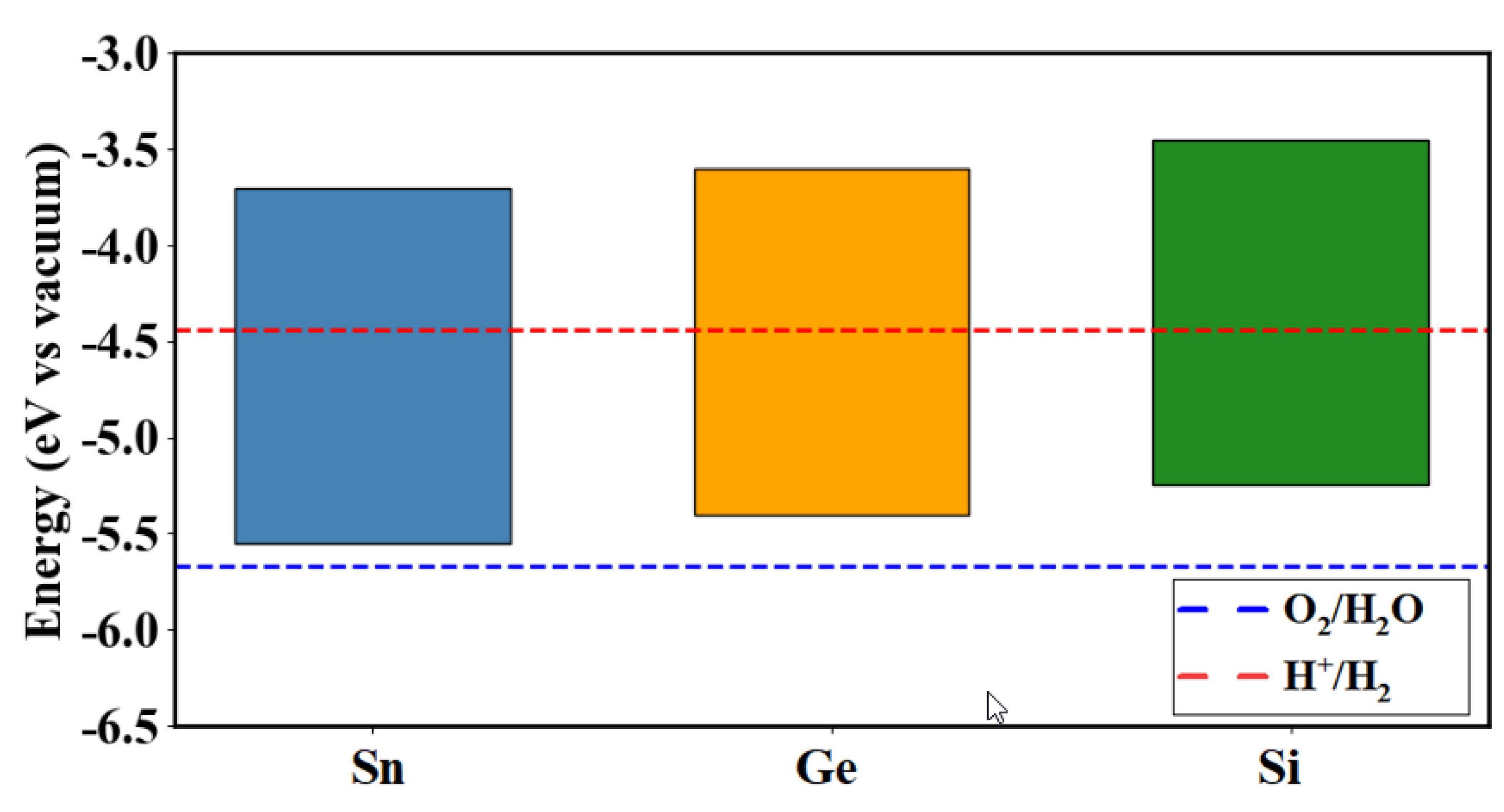
In the context of photovoltaic applications, such as chalcogenide or perovskite-based solar cells, the energy level diagram plays a crucial role in the design of heterojunctions. Efficient carrier transfer requires the alignment of the valence band maximum (VBM) and conduction band minimum (CBM) of the absorbing material with the energy levels of the electron transport layer (ETL) and hole transport layer (HTL). For instance, an excessively low VBM can create a barrier for hole extraction, thereby reducing the overall efficiency of the device. A comparison with well-known materials, such as CZTS (VBM ~-5.2 eV) or perovskites (VBM ~-5.4 eV), suggests that Cu2NiXSe4 compounds could be promising candidates for thin-film solar cells, provided their electronic structure is optimized and compatible transport layers are selected.
Figure 9 presents a three-dimensional density of states (DOS) diagram for the three chalcogenide-type compounds in the Cu2Ni(Sn,Ge,Si)Se4 family, providing valuable information about the electronic structure of these materials and enabling a comparative analysis of their properties. The calculated DOS profiles correlate with the band structure features (Figure 6), providing a consistent picture of the evolving electronic states across the series.
Figure 9.
Comparative analysis of the density of states (DOS) of the Cu2Ni(Sn, Ge, Si)Se4 system.
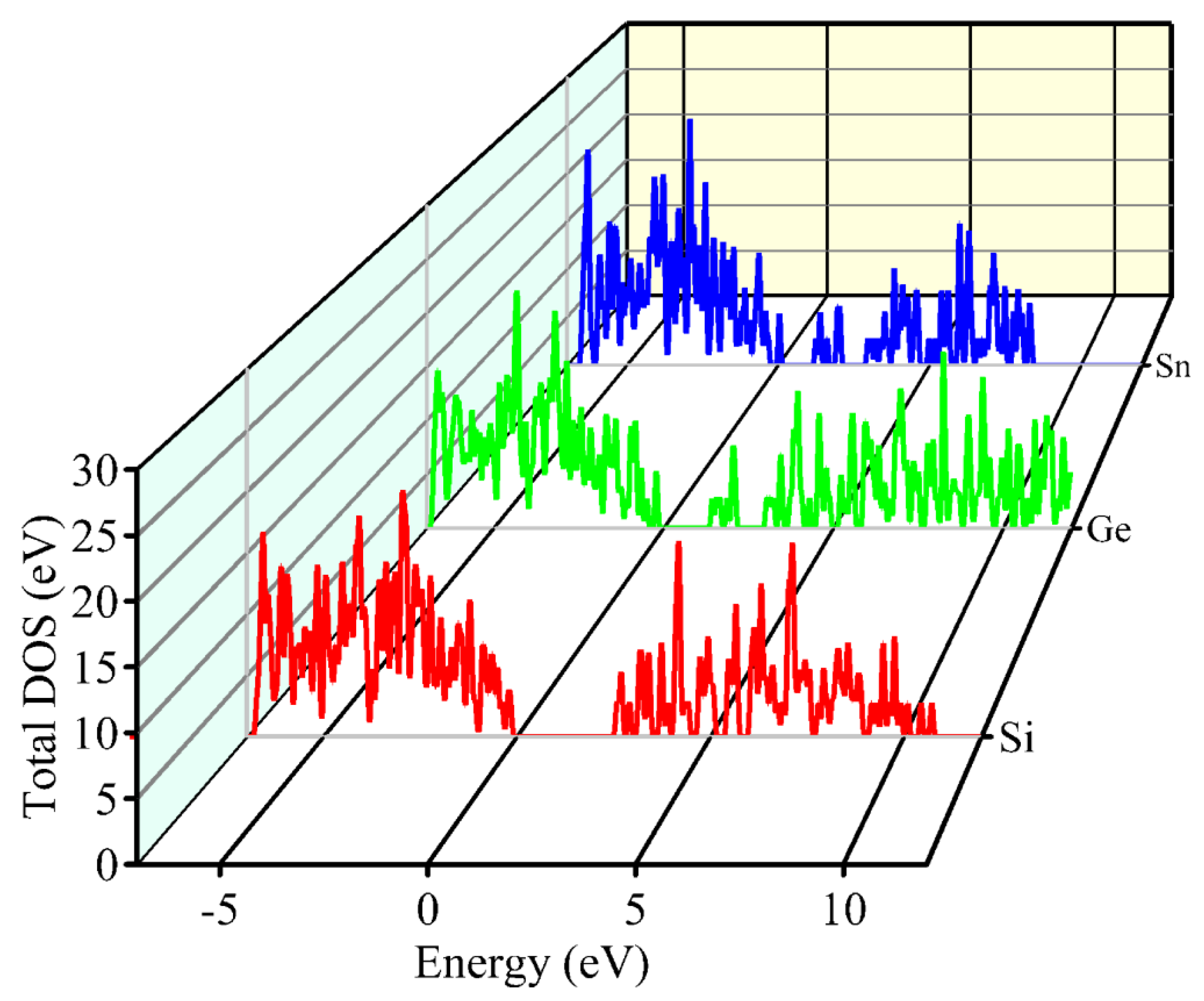
The primary difference between the compounds Cu2NiSiSe4, Cu2NiGeSe4, and Cu2NiSnSe4 lies in the changes to their electronic structure, particularly in the vicinity of the band gap. As the atomic number of the central atom increases (Si → Ge → Sn), a narrowing of the band gap is observed, which enhances the absorption of the solar spectrum and improves the efficiency of solar panels. Additionally, the density of states near the Fermi level changes, influencing the conductivity of the material and the generation of charge carriers. This effect is significant for optimizing materials for use in solar cells and electronics [68-71]. A comparative analysis of the density of states for these compounds helps evaluate their potential as active layers in solar cells and in the creation of heterostructures. To better understand the contribution of each specific element to the formation of states in the valence and conduction bands, partial density of states for Cu2NiSnSe4, Cu2NiGeSe4, and Cu2NiSiSe4 are presented in Figure 10 (a-c).
The partial density of states (PDOS) graphs for Cu2NiSnSe4 (a), Cu2NiGeSe4 (b), and Cu2NiSiSe4 (c) presented in the figure show the contributions of Cu and Ni (particularly their d-orbitals), as well as the p-orbitals of Se and elements X (Sn, Ge, Si) to the formation of the electronic structure. The analysis reveals that the valence band is primarily formed by the hybridization of the p-orbitals of Se and X, while the conduction band is determined by the d-states of Cu and Ni. The projected density of states (PDOS) results also support the observed trends in the band structure (Figure 6) and effective mass analysis (Figure 7). Specifically, the increasing contribution of Ni-3d orbitals near the conduction band minimum (CBM), particularly in Cu₂NiSiSe₄, correlates with the enhanced localization of conduction states and the observed increase in electron effective mass. Simultaneously, the narrowing of the valence band and increasing dominance of Se-4p and X-s/p (X = Ge, Si) orbitals near the valence band maximum (VBM) results in flatter valence bands and larger hole effective masses. These effects are consistent with the more pronounced curvature of the bands in Cu2NiSnSe4 (indicative of lighter carriers) and the flatter bands in Cu2NiSiSe4.
Furthermore, as the atomic number of the central atom decreases (Sn → Ge → Si), the DOS near the Fermi level becomes more asymmetric and sparser, reflecting the wider bandgap and more semiconductor-like behavior. The reduction in the density of states around the Fermi energy supports the transition from a weakly metallic (or narrow-gap) character in Cu2NiSnSe4 to a non-magnetic wide-bandgap semiconductor character in Cu2NiSiSe4. This demonstrates how the nature of the chemical bonds and orbital hybridization not only governs the energy dispersion in the band structure but also directly impacts the material’s transport and optical behavior.
The results of the density of states calculations, performed considering spin polarization (Figure 11), allow for the analysis of the distribution of electronic states across spin sublevels -spin-up (upper curves, black line) and spin-down (lower curves, red line). The Fermi level is set to zero.
The analysis of the results presented in Figure 11(a) shows that the compound Cu2NiSnSe4 exhibits a pronounced asymmetry between the density of states for the spin-up and spin-down states near the Fermi level. The upper and lower spins have different intensity distributions, indicating the presence of spontaneous spin polarization and, consequently, ferromagnetic behavior of the material. It is also evident that the density of states at the Fermi level remains non-zero for both spin-up and spin-down states, suggesting a metallic or semi-metallic nature of the compound. In the case of Cu2NiGeSe4 (Figure 11(b)), spin asymmetry is still present, although it is weaker compared to Cu2NiSnSe4. The upper and lower spins show more similar distributions, although the density of states at the Fermi level remains non-zero. This indicates a weakening of the magnetic order, a possible reduction in the magnetic moment, and the retention of conductive properties. In Figure 11(c), for Cu2NiSiSe4, the densities of states for the upper and lower spins are nearly symmetric with respect to the Fermi level. A significant reduction in the total density of states near the Fermi level is observed, especially compared to the previous compounds. This pattern indicates the disappearance of spontaneous magnetic polarization and the formation of a non-magnetic state [72-80]. Moreover, the decrease in the density of states near the Fermi level suggests the presence of a band gap and a semiconductor character for the material.
Thus, as one moves from Cu2NiSnSe4 to Cu2NiSiSe4, a clear trend is observed: the density of states at the Fermi level decreases, and the distributions of the upper and lower spins become more aligned. This indicates a gradual transition from a ferromagnetic metallic state to a non-magnetic semiconductor, highlighting the influence of the Sn, Ge, Si on the magnetic and electronic properties of Cu2Ni(Sn, Ge, Si)Se4 compounds.
CONCLUSIONS
This study demonstrates that Cu2Ni(Sn,Ge,Si)Se4 kesterites possess highly tunable electronic structures, with band gaps systematically adjustable from 0.79 eV (Sn) to 2.35 eV (Si), making them promising candidates for active layers in thin-film solar cells. The variation in chemical composition not only enables precise tuning of the band gap but also enhances the transport properties, with effective masses of electrons and holes showing a clear trend as the composition changes. Additionally, the transition from weakly magnetic behavior in Cu2NiSnSe4 to a non-magnetic semiconductor character in Cu2NiSiSe4 highlights the materials' structural flexibility and their potential compatibility with existing transport layers.To complement the structural analysis, a comparative evaluation of the total and formation energies of the Cu2Ni(Sn,Ge,Si)Se4 compounds was performed to assess their relative thermodynamic stability. The results indicate a clear trend of decreasing total and formation energies when moving from Sn to Ge and Si, reflecting enhanced energetic stability for compounds with smaller group-IV elements. This trend, along with the observed reduction in lattice volume and stronger X–Se bonding, supports the structural integrity of Cu2NiSiSe4 as the most stable member of the series. These findings provide a solid theoretical foundation for the future experimental synthesis and integration of Cu2Ni(Sn,Ge,Si)Se4 kesterites into solar cell architectures, offering a versatile platform for the next generation of environmentally friendly energy solutions. A detailed analysis of thermodynamic, optical, and elastic properties is currently in progress and will be presented in a forthcoming publication, building upon the electronic structure results described here. The tunable band gaps and electronic structures of Cu2Ni(Sn,Ge,Si)Se4 make these materials ideal candidates not only for single-junction solar cells, but also for tandem architectures and infrared photodetectors. In particular, Cu2NiSnSe4 may serve well in IR-sensing, while Cu2NiSiSe4 is optimized for visible-light photovoltaic absorption.
Funding
This work was supported by the International Science and Technology Center (grant no. TJ-2726).
Conflicts of Interest
The authors declare no conflict of interest.
References
- Mitzi, D.B.; et al. The path to high-efficiency kesterite solar cells. Nature Photonics 2011, 5, 645–653. [Google Scholar]
- Green, M.A.; Dunlop, E.D.; Hohl-Ebinger, J.; Yoshita, M.; Kopidakis, N.; Hao, X. Solar cell efficiency tables (version 57). Progress in Photovoltaics: Research and Applications 2021, 29, 3–15. [Google Scholar] [CrossRef]
- Scragg, J.J.; Choubrac, L.; Lafond, A.; Ericson, T.; Platzer-Björkman, C. A low-temperature order-disorder transition in Cu₂ZnSnS₄ thin films. Applied Physics Letters 2014, 104, 041901. [Google Scholar] [CrossRef]
- Tanaka, K.; Oonuki, M.; Moritake, N.; Uchiki, H. Cu₂ZnSnS₄ thin film solar cells prepared by non-vacuum processing. Solar Energy Materials and Solar Cells 2009, 93, 583–587. [Google Scholar] [CrossRef]
- Kumar, A.; et al. Structural and optical properties of Cu₂NiSnS₄ thin films synthesized by spray pyrolysis. Materials Chemistry and Physics, 180, 239-245.
- Heyd, J.; Scuseria, G.E.; Ernzerhof, M. Hybrid functionals based on a screened Coulomb potential. The Journal of Chemical Physics 2003, 118, 8207–8215. [Google Scholar] [CrossRef]
- Wu, T.; Chen, S.; Su, Z.; Wang, Z.; Luo, P.; Zheng, Z.; Liang, G. Heat treatment in an oxygen-rich environment to suppress deep-level traps in Cu₂ZnSnS₄ solar cell with 11.51% certified efficiency. Nature Energy 2025, 1-11.
- Zhao, Y.; Chen, X.; Chen, S.; Zheng, Z.; Su, Z.; Ma, H.; Liang, G. Energy band alignment and defect synergistic regulation enable air-solution-processed kesterite solar cells with the lowest VOC deficit. Advanced Materials 2025, 37, 2409327. [Google Scholar] [CrossRef]
- Liang, A.; Jian, Y.; Zhao, Y.; Chen, S.; Zhao, J.; Zheng, Z.; Liang, G. An effective precursor-solutioned strategy for developing Cu₂ZnSn(S,Se)₄ thin film toward high efficiency solar cell. Advanced Energy Materials 2025, 15, 2403950. [Google Scholar] [CrossRef]
- Su, Z.; Liang, G.; Fan, P.; Luo, J.; Zheng, Z.; Xie, Z.; Liu, F. Device postannealing enabling over 12% efficient solution-processed Cu₂ZnSnS₄ solar cells with Cd²⁺ substitution. Advanced Materials 2020, 32, 2000121. [Google Scholar] [CrossRef]
- Yu, Z.; Li, C.; Chen, S.; Zheng, Z.; Fan, P.; Li, Y.; Liang, G. Unveiling the selenization reaction mechanisms in ambient air-processed highly efficient kesterite solar cells. Advanced Energy Materials 2023, 13, 2300521. [Google Scholar] [CrossRef]
- Ye, F.; He, C.; Wu, T.; Chen, S.; Su, Z.; Zhang, X.; Liang, G. Sputtering deposited and energy band matched ZnSnN₂ buffer layers for highly efficient Cd-free Cu₂ZnSnS₄ solar cells. Advanced Functional Materials 2024, 34, 2402762. [Google Scholar] [CrossRef]
- Liang, G.X.; Li, C.H.; Zhao, J.; Fu, Y.; Yu, Z.X.; Zheng, Z.H.; Chen, S. Self-powered broadband kesterite photodetector with ultrahigh specific detectivity for weak light applications. SusMat 2023, 3, 682–696. [Google Scholar] [CrossRef]
- Liang, G.; Li, Z.; Ishaq, M.; Zheng, Z.; Su, Z.; Ma, H.; Chen, S. Charge separation enhancement enables record photocurrent density in Cu₂ZnSn(S,Se)₄ photocathodes for efficient solar hydrogen production. Advanced Energy Materials 2023, 13, 2300215. [Google Scholar] [CrossRef]
- Li, Y.; Wang, Z.; Zhao, Y.; Luo, D.; Zhang, X.; Zhao, J.; Liang, G. Potassium doping for grain boundary passivation and defect suppression enables highly-efficient kesterite solar cells. Chinese Chemical Letters 2024, 35, 109468. [Google Scholar] [CrossRef]
- Chen, C.; Liu, L.; Huang, T.; Tu, B.; Li, H.; He, Q.; Guo, F. Dual interfacial design enables efficient and stable semitransparent wide-bandgap perovskite solar cells with scalable-coated silver nanowire contact for tandem applications. SusMat 2025, 5, e256. [Google Scholar] [CrossRef]
- Wu, Q.; Li, C.; Chen, S.; Su, Z.; Abbas, M.; Chen, C.; Liang, G. Tailoring a back-contact barrier for a self-powered broadband kesterite photodetector with ultralow dark current enabling ultra-weak-light detection. Carbon Energy 2025, e70001. [Google Scholar] [CrossRef]
- Liu, X.; Ma, C.; Xin, H.; Ding, L. Solution-processed CuIn(S,Se)₂ solar cells on transparent electrode offering 9.4% efficiency. Journal of Semiconductors 2023, 44, 80501. [Google Scholar] [CrossRef]
- Bendahah, A.; Bensaid, D.; Yhaia, A.; Khadidja, M.; Noureddine, M.; Bendouma, D.; Al-Douri, Y. First-principles calculations to investigate structural, electronic, piezoelectric and optical properties of Sc-doped GaN. *Emergent Materials 2024, 1-9.
- Marzougui, B.; Smida, Y.B.; Ferhi, M.; Ferjani, H.; Onwudiwe, D.; Hamzaoui, A.H.; Al Douri, Y. Photoluminescence properties of Pr-doped LaAsO₄: An experimental and theoretical study employing density functional theory. Ceramics International 2024, 50, 26435–26445. [Google Scholar] [CrossRef]
- Al-Essa, S.; Essaoud, S.S.; Bouhemadou, A.; Ketfi, M.E.; Maabed, S.; Djilani, F.; Al-Douri, Y. An ab initio analysis of the electronic, optical, and thermoelectric characteristics of the Zintl phase CsGaSb₂. Physica Scripta 2024, 99, 095996. [Google Scholar] [CrossRef]
- Smida, Y.B.; Marzougui, B.; Driss, M.; Onwudiwe, D.C.; Al-Douri, Y. Exploring the optoelectronic potential of M₂SnX₃F₂ (M= Sr, Ba; X= S, Se) compounds through first-principles analysis of structural, electronic, and optical properties. Chemistry Africa 2024, 7, 491–503. [Google Scholar] [CrossRef]
- Abdelakader, A.; Ahmed, B.; Noureddine, M.; Mokhtar, B.; Abdelhalim, Z.; Omar, M.; Al-Douri, Y. Theoretical investigations of electronic, thermodynamic and thermoelectric properties of filled skutterudites ThFe₄P₁₂ and CeFe₄P₁₂ using DFT calculations. Solid State Communications 2024, 380, 115435. [Google Scholar] [CrossRef]
- Allali, D.; Abdelmadjid, B.; Saber, S.E.; Bahri, D.; Zerarga, F.; Amari, R.; Al-Douri, Y. A first-principles investigation on the structural, electronic and optical characteristics of tetragonal compounds XAgO (X= Li, Na, K, Rb). Computational Condensed Matter 2024, 38, e00876. [Google Scholar] [CrossRef]
- Allaf, H.; Radjai, M.; Allali, D.; Bouhemadou, A.; Essaoud, S.S.; Bin-Omran, S.; Al-Douri, Y. Ab initio predictions of pressure-dependent structural, elastic, and thermodynamic properties of CaLiX₃ (X= Cl, Br, and I) halide perovskites. Computational Condensed Matter 2023, 37, e00850. [Google Scholar] [CrossRef]
- Ferjani, H.; Smida, Y.B.; Al-Douri, Y. First-principles calculations to investigate the effect of van der Waals interactions on the crystal and electronic structures of tin-based 0D hybrid perovskites. Inorganics 2022, 10, 155. [Google Scholar] [CrossRef]
- Samia, R.; Yahia, A.; Ahmed, B.; Mokhtar, B.; Noureddine, M.; Mohamed, L.; Al-Douri, Y. Electronic, elastic and piezoelectric properties calculations of perovskites materials type BiXO₃ (X= Al, Sc): DFT and DFPT investigations. Chemical Physics 2023, 573, 111998. [Google Scholar] [CrossRef]
- Gaid, F.O.; Boufadi, F.Z.; Tayebi, N.; Ameri, M.; Mentefa, A.; Bellagoun, L.; Al-Douri, Y. Theoretical investigation of structural, electronic, elastic, magnetic, thermodynamic, and thermoelectric properties of Ru₂MnNb Heusler alloy: FP-LMTO method. Emergent Materials 2022, 5, 1065–1073. [Google Scholar] [CrossRef]
- Drici, L. First-principles calculations of structural, elastic, electronic, and optical properties of CaYP (Y= Cu, Ag) Heusler alloys. Emergent Materials 2021, 4, 1–12. [Google Scholar] [CrossRef]
- Saim, A.; Belkharroubi, F.; Boufadi, F.Z.; Ameri, I.; Blaha, L.F.; Tebboune, A.; Abd El-Rehim, A.F. Investigation of the structural, elastic, electronic, and optical properties of half-heusler CaMgZ (Z= C, Si, Ge, Sn, Pb) compounds. Journal of Electronic Materials 2022, 51, 4014–4028. [Google Scholar] [CrossRef]
- Samia, L.; Belkharroubi, F.; Ibrahim, A.; Lamia, B.F.; Saim, A.; Maizia, A.; Al-Douri, Y. Investigation of structural, elastic, electronic, and magnetic proprieties for X₂LuSb (X= Mn and Ir) full-Heusler alloys. Emergent Materials 2022, 5, 537–551. [Google Scholar] [CrossRef]
- Zerarga, F.; Allali, D.; Bouhemadou, A.; Khenata, R.; Deghfel, B.; Essaoud, S.S.; Naqib, S.H. Ab initio study of the pressure dependence of mechanical and thermodynamic properties of GeB₂O₄ (B= Mg, Zn and Cd) spinel crystals. Computational Condensed Matter 2022, 32, e00705. [Google Scholar] [CrossRef]
- Benamara, A.; Moulay, N.; Azzaz, Y.; Ameri, M.; Rabah, M.; Al-Douri, Y.; Moumen, C. Elastic, electronic, thermal and magnetic investigations of PrX₂ (X= Fe, Ru) superconductors materials. Materials Today Communications 2023, 35, 105545. [Google Scholar] [CrossRef]
- Al-Hawarin, J.I.; Abu-Yamin, A.A.; Abu-Saleh, A.A.A.A.; Saraireh, I.A.; Almatarneh, M.H.; Hasan, M.; Al-Douri, Y. Synthesis, characterization, and DFT calculations of a new sulfamethoxazole schiff base and its metal complexes. Materials 2023, 16, 5160. [Google Scholar] [CrossRef]
- Allali, D.; Amari, R.; Bouhemadou, A.; Boukhari, A.; Deghfel, B.; Essaoud, S.S.; Al-Douri, Y. Ab initio investigation of structural, elastic, and thermodynamic characteristics of tetragonal XAgO compounds (X= Li, Na, K, Rb). Physica Scripta 2023, 98, 115905. [Google Scholar] [CrossRef]
- Liu, X.; et al. Cu₂NiGeSe₄: A new kesterite material for photovoltaic applications. Solar Energy Materials and Solar Cells 2021, 230, 111234. [Google Scholar]
- Berri, S. Search for New Half-Metallic Ferromagnets in Quaternary Diamond-Like Compounds I–II 2–III–VI 4 and I 2–II–IV–VI 4 (I= Cu; II= Mn, Fe, Co; III= In; IV= Ge, Sn; VI= S, Se, Te). Journal of Superconductivity and Novel Magnetism, 31 2018, 1941-1947.
- Berri, S.; Bouarissa, N.; Oumertem, M.; Chami, S. First-principles investigation of structural, electronic, optical and thermodynamic properties of KAg2SbS4. Computational Condensed Matter 2019, 19, e00365. [Google Scholar] [CrossRef]
- Berri, S.; Amari, R.; Bouarissa, N.; Miloud, I. Study on quaternary diamond-like Li2CaGeO4 properties for optoelectronic applications. Computational Condensed Matter 2022, 30, e00646. [Google Scholar] [CrossRef]
- Kresse, G.; Furthmüller, J. Efficient iterative schemes for ab initio total-energy calculations using a plane-wave basis set. Physical review B 1996, 54, 11169. [Google Scholar] [CrossRef]
- Blöchl, P.E. Projector augmented-wave method. Physical review B 1994, 50, 17953. [Google Scholar] [CrossRef]
- Sun, J.; Ruzsinszky, A.; Perdew, J.P. Strongly constrained and appropriately normed semilocal density functional. Physical review letters 2015, 115, 036402. [Google Scholar] [CrossRef]
- Heyd, J.; Scuseria, G.E.; Ernzerhof, M. Hybrid functionals based on a screened Coulomb potential. The Journal of chemical physics 2003, 118, 8207–8215. [Google Scholar] [CrossRef]
- del Campo, J. M., Gázquez, J. L., Trickey, S. B., & Vela, A. (2012). Non-empirical improvement of PBE and its hybrid PBE0 for general description of molecular properties. The Journal of chemical physics, 136(10).
- Momma, K.; Izumi, F. VESTA 3 for three-dimensional visualization of crystal, volumetric and morphology data. Applied Crystallography 2011, 44, 1272–1276. [Google Scholar] [CrossRef]
- Moroz, N. (2017). Engineered transition metal chalcogenides for photovoltaic, thermoelectric, and magnetic applications. PhD diss.
- Tajima, S.; Ueno, T.; Matsubara, K.; Yoshida, T.; Shibata, H. Structural and optoelectronic properties of Cu2NiSn(S,Se)4 kesterite films for photovoltaic applications. Sol, Energy Mater, Sol, Cells 2018, 186, 134–140. [Google Scholar]
- Persson, C. Electronic and optical properties of Cu-based quaternary compounds for thin film solar cells. J, Appl, Phys 2010, 107, 053710. [Google Scholar] [CrossRef]
- Scragg, J.J.; Larsen, J.K.; Kumar, M.; Persson, C.; Sendler, J.; Siebentritt, S.; Platzer Björkman, C. Cu–Zn disorder and band gap fluctuations in Cu2ZnSn(S, Se)4: Theoretical and experimental investigations. physica status solidi (b) 2016, 253, 247–254. [Google Scholar] [CrossRef]
- Dasgupta, S.; Shahi, C.; Bhetwal, P.; Perdew, J.P.; Paesani, F. How good is the density-corrected SCAN functional for neutral and ionic aqueous systems, and what is so right about the Hartree–Fock density? . Journal of Chemical Theory and Computation 2022, 18, 4745–4761. [Google Scholar] [CrossRef] [PubMed]
- Kingsbury, R.; Gupta, A.S.; Bartel, C.J.; Munro, J.M.; Dwaraknath, S.; Horton, M.; Persson, K.A. Performance comparison of r2 SCAN and SCAN metaGGA density functionals for solid materials via an automated, high-throughput computational workflow. Physical Review Materials 2022, 6, 013801. [Google Scholar] [CrossRef]
- Hinuma, Y.; Hayashi, H.; Kumagai, Y.; Tanaka, I.; Oba, F. Comparison of approximations in density functional theory calculations: Energetics and structure of binary oxides. Physical Review B 2017, 96, 094102. [Google Scholar] [CrossRef]
- Shahi, C.; Sun, J.; Perdew, J.P. Accurate critical pressures for structural phase transitions of group IV, III-V, and II-VI compounds from the SCAN density functional. Physical Review B 2018, 97, 094111. [Google Scholar] [CrossRef]
- Ekholm, M.; Gambino, D.; Jönsson, H.J. M.; Tasnádi, F.; Alling, B.; Abrikosov, I.A. Assessing the SCAN functional for itinerant electron ferromagnets. Physical Review B 2018, 98, 094413. [Google Scholar] [CrossRef]
- Koller, D.; Tran, F.; Blaha, P. Merits and limits of the modified Becke-Johnson exchange potential. Physical Review B—Condensed Matter and Materials Physics 2011, 83, 195134. [Google Scholar] [CrossRef]
- Souza, J.S.; Lima, A.F. Combining mBJ exchange potential and bootstrap kernel of TDDFT to compute optical spectra of solids. Computational Condensed Matter 2024, 39, e00909. [Google Scholar] [CrossRef]
- Safa, R.K. G.; Aliabad, H.R.; Baghani, H.R.; Özdemir, E.G.; Arzefooni, A.A.; Sadati, S.Z. Optoelectronic, thermoelectric, and EFG of atomic nuclei of trityl-functionalized fullerene C60 using GGA and mBJ approximations. Physica B: Condensed Matter 2025, 704, 417053. [Google Scholar] [CrossRef]
- 이재호. (2016). Characteristics of the higher-k Hf-Zr-O dielectric materials on Si Ge substrates and their application in 3-dimensional Tri-Gate FET devices (Doctoral dissertation, 서울대학교 대학원).
- Ahmed, I.; Prakash, K.; Mobin, S.M. (2025). Lead-free perovskites for solar cells applications: recent progress, ongoing challenges, and strategic approaches. Chemical Communications.
- Aouiche, Abdelaziz. "Semiconductor Physics." (2024).
- Chibani, M.; Benamara, S.; Zitoune, H.; Lasmi, M.; Benchalal, L.; Lamiri, L.; Samah, M. Electronic and Magnetic Properties of Small Nickel Clusters Ni n (n≤ 15): First Priciple Study. International Journal of Quantum Chemistry 2025, 125, e70007. [Google Scholar] [CrossRef]
- Ghosh, A.; Biswas, A.; Thangavel, R.; Udayabhanu, G. Photo-electrochemical properties and electronic band structure of kesterite copper chalcogenide Cu 2–II–Sn–S 4 (II= Fe, Co, Ni) thin films. RSC Advances 2016, 6, 96025–96034. [Google Scholar] [CrossRef]
- Østrøm, I.; Favaro, M.; Seyfouri, M.; Burr, P. Hoex, B. Electrostatic and Electronic Effects on Doped Nickel Oxide Nanofilms for Water Oxidation. Journal of the American Chemical Society 2025, 147, 4, 3593–3606. [Google Scholar]
- Sofi, M.Y.; Khan, M.S.; Ali, J.; Khan, M.A. Unlocking the role of 3d electrons on ferromagnetism and spin-dependent transport properties in K2GeNiX6 (X= Br, I) for spintronics and thermoelectric applications. Journal of Physics and Chemistry of Solids 2024, 192, 112022. [Google Scholar] [CrossRef]
- Kerrai, H.; Zaim, A.; Kerouad, M. Half-metallic ferromagnetic and optical properties of YScO3 (Y= Ni, Pd, and Pt) perovskite: A first principles study. Vacuum 2024, 226, 113341. [Google Scholar] [CrossRef]
- Espinel Pérez, N.M.; Vera López, E.; Gómez Cuaspud, J.A.; Carda Castelló, J.B. A review of recent advances of kesterite thin films based on magnesium, iron and nickel for photovoltaic application: insights into synthesis, characterization and optoelectronic properties. Clean Energy 2024, 8, 217–238. [Google Scholar] [CrossRef]
- Xu, X.; Zhou, J.; Yin, K.; Wang, J.; Lou, L.; Li, D.; Meng, Q. 12. 84% efficiency flexible kesterite solar cells by heterojunction interface regulation. Advanced Energy Materials 2023, 13, 2301701. [Google Scholar]
- Zuo, G.; Abdalla, H.; Kemerink, M. Impact of doping on the density of states and the mobility in organic semiconductors. Physical Review B 2016, 93, 235203. [Google Scholar] [CrossRef]
- Marshak, A.H.; Van Vliet, C.M. Electrical current and carrier density in degenerate materials with nonuniform band structure. Proceedings of the IEEE 1984, 72, 148–164. [Google Scholar] [CrossRef]
- Sathyanarayanan, S.; Pandiaraj, S.; Abeykoon, C.; Alzahrani, K.E.; Alodhayb, A.N.; Grace, A.N. Investigating the potential of perovskite-based redox electrolytes for dye sensitised solar cells: An in-depth analysis using mathematical and DFT techniques. Solar Energy 2025, 288, 113267. [Google Scholar] [CrossRef]
- Noman, M.; Shahzaib, M.; Jan, S.T.; Khan, Z.; Ismail, M.; Khan, A.D. Optimizing band gap, electron affinity, carrier mobility for improved performance of formamidinium lead tri-iodide perovskite solar cells. Materials Science and Engineering: B 2024, 300, 117114. [Google Scholar] [CrossRef]
- Xu, H.; Wang, M.; Yu, Z.G.; Wang, K.; Hu, B. Magnetic field effects on excited states, charge transport, and electrical polarization in organic semiconductors in spin and orbital regimes. Advances in Physics 2019, 68, 49–121. [Google Scholar] [CrossRef]
- Volnianska, O.; Boguslawski, P. Magnetism of solids resulting from spin polarization of p orbitals. Journal of Physics: Condensed Matter 2010, 22, 073202. [Google Scholar] [CrossRef]
- Bansmann, J.; Baker, S.H.; Binns, C.; Blackman, J.A.; Bucher, J.P.; Dorantes-Dávila, J.; Xie, Y. Magnetic and structural properties of isolated and assembled clusters. Surface Science Reports 2005, 56(6-7), 189-275.
- ELAGGOUNE.; W (2024). Ab-initio study of the properties of the 3D SrS-based mono-doped and co-doped compounds. A comparative study of the 2D and 3D mono-doped compounds (Doctoral dissertation).
- Haas, C. Magnetic semiconductors. Critical Reviews in Solid State and Material Sciences 1970, 1;1(1), 47-98.
- Nematov, D. Bandgap tuning and analysis of the electronic structure of the Cu2NiXS4 (X= Sn, Ge, Si) system: mBJ accuracy with DFT expense. Chemistry of Inorganic Materials 2023, 1, 100001. [Google Scholar] [CrossRef]
- Nematov, D.; Burhonzoda, A.; Khusenov, M.; Kholmurodov, K.; Doroshkevych, A.; Doroshkevych, N.; Ibrahim, M. Molecular dynamics simulations of the DNA radiation damage and conformation behavior on a zirconium dioxide surface. Egyptian Journal of Chemistry 2019, 62, 149–161. [Google Scholar] [CrossRef]
- Nematov, D. ; HojamberdievM. (2025). Machine Learning-Driven Materials Discovery: Unlocking Next-Generation Functional Materials-A minireview. arXiv preprint arXiv:2503. 1897. [Google Scholar]
- Younis, M.; Abdullah, M.; Dai, S.; Iqbal, M.A.; Tang, W.; Sohail, M. T.; Zeng, Y.J. (2025). Magnetoresistance in 2D Magnetic Materials: From Fundamentals to Applications. Advanced Functional Materials, 2417282.
Figure 1.
Convergence of the total energy of the Cu₂NiGeSe₄ crystal structure as a function of the plane-wave cutoff energy (ENCUT), calculated using Monkhorst-Pack (blue) and Γ-centered (red) k-point sampling schemes.
Figure 1.
Convergence of the total energy of the Cu₂NiGeSe₄ crystal structure as a function of the plane-wave cutoff energy (ENCUT), calculated using Monkhorst-Pack (blue) and Γ-centered (red) k-point sampling schemes.

Figure 2.
Convergence of the total energy of the Cu2NiGeSe4 crystal structure as a function of k-point mesh density, constructed using the Monkhorst-Pack scheme (blue) and Gamma-centered scheme (red).
Figure 2.
Convergence of the total energy of the Cu2NiGeSe4 crystal structure as a function of k-point mesh density, constructed using the Monkhorst-Pack scheme (blue) and Gamma-centered scheme (red).
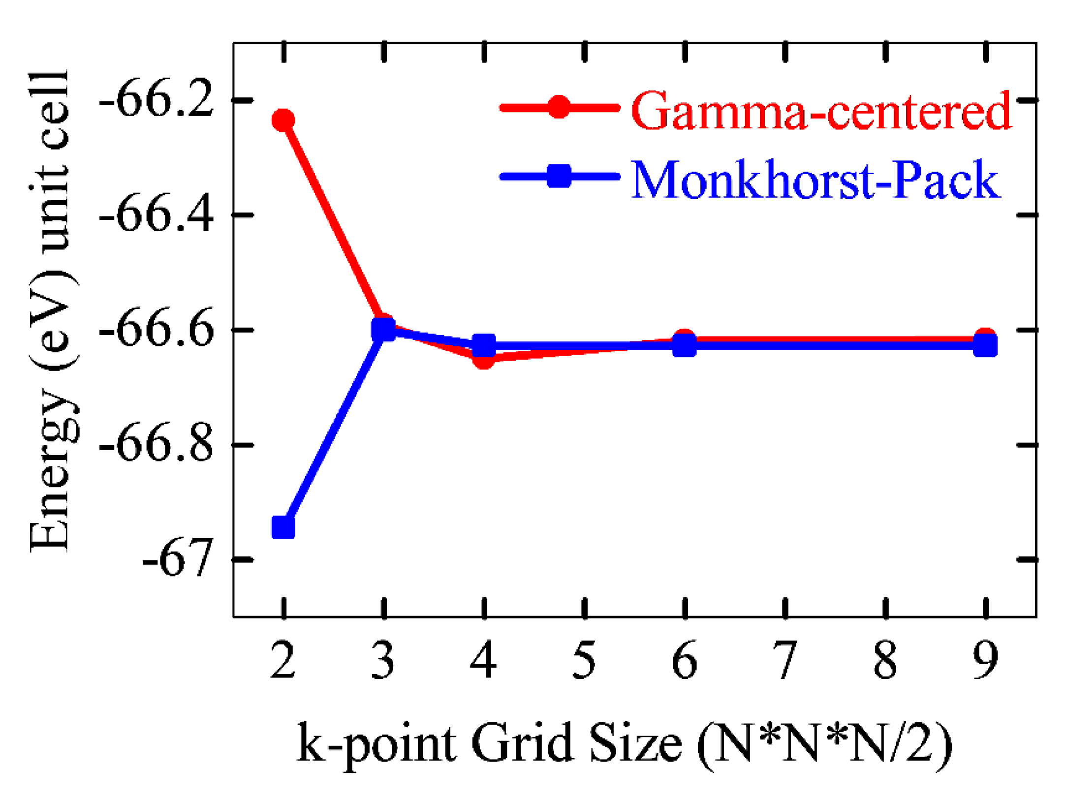
Figure 3.
Crystal structure illustration and polyhedral model of the optimized structural unit of Cu2NiSnSe4 (left), and coordination environment of the central atoms in XSe4 tetrahedra (X = Sn, Ge, Si), visualized using VESTA (right). The X–Se bond lengths are given in angstroms (Å).
Figure 3.
Crystal structure illustration and polyhedral model of the optimized structural unit of Cu2NiSnSe4 (left), and coordination environment of the central atoms in XSe4 tetrahedra (X = Sn, Ge, Si), visualized using VESTA (right). The X–Se bond lengths are given in angstroms (Å).
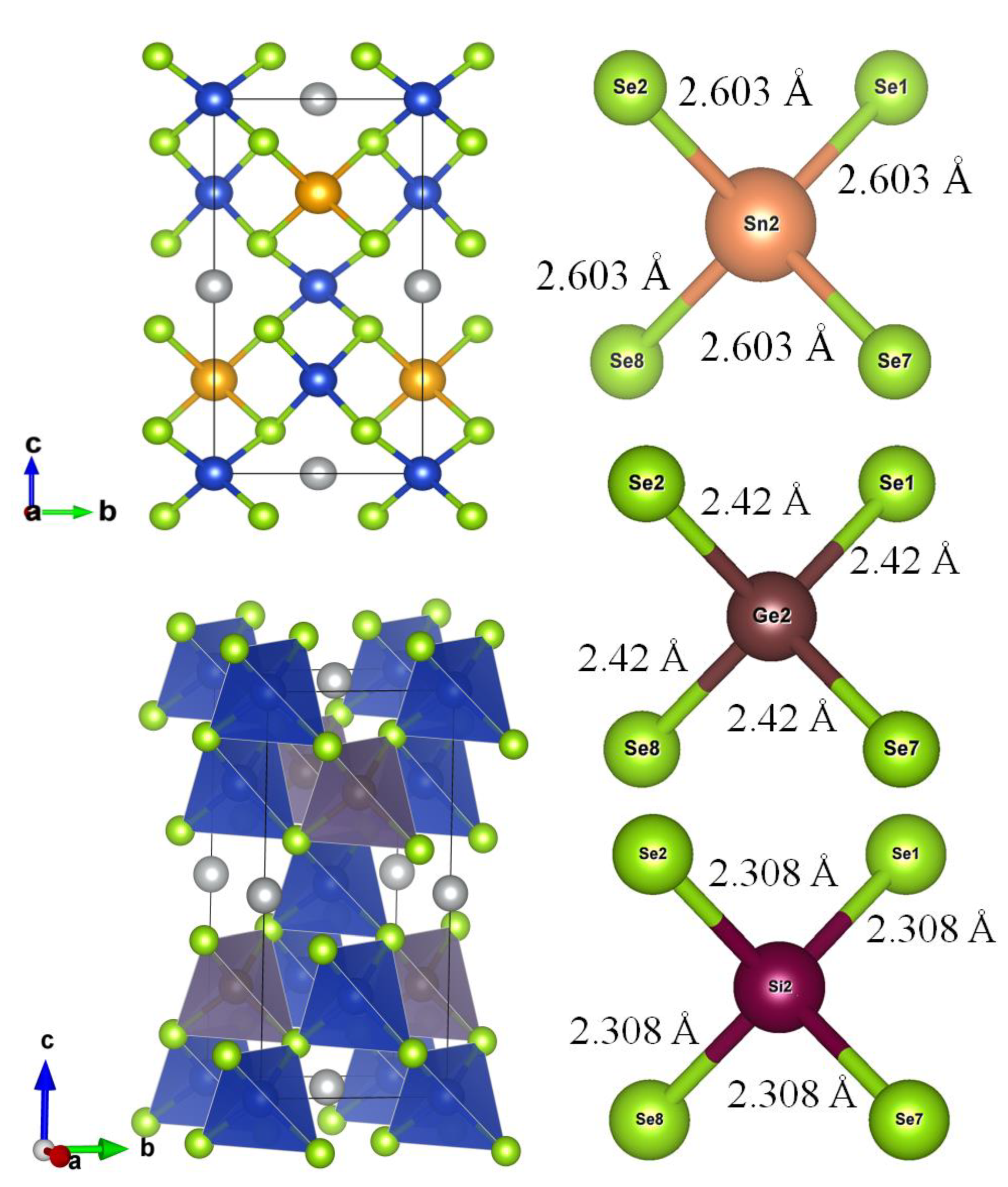
Figure 4.
Dependence of the unit cell volume of the Cu2Ni(Sn, Ge, Si)Se4 system on the composition, calculated using the SCAN functional.
Figure 4.
Dependence of the unit cell volume of the Cu2Ni(Sn, Ge, Si)Se4 system on the composition, calculated using the SCAN functional.
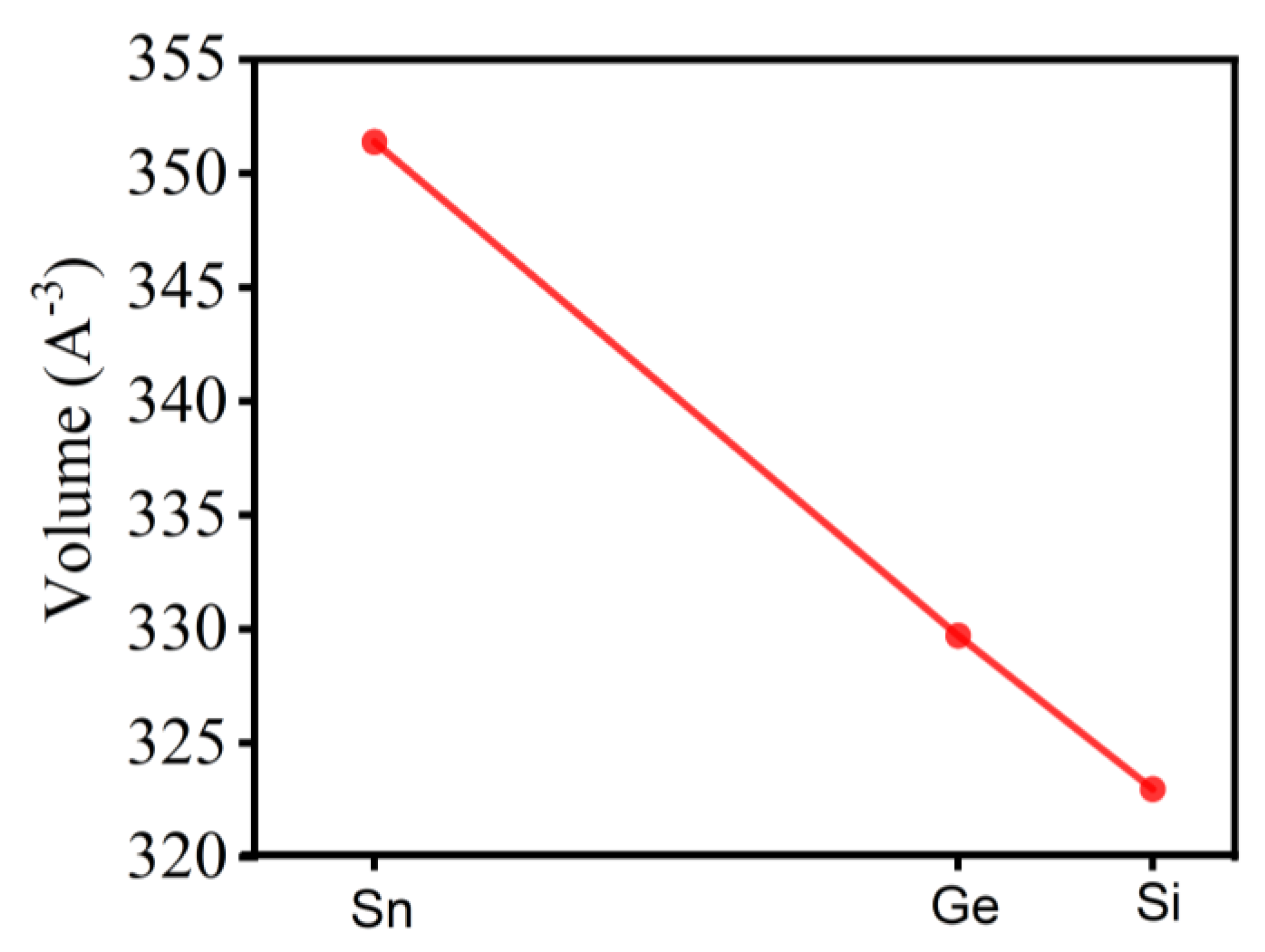
Figure 5.
Calculated X-ray diffraction patterns of the Cu2Ni(Sn, Ge, Si)Se4 compounds: intensity versus diffraction angle 2θ.
Figure 5.
Calculated X-ray diffraction patterns of the Cu2Ni(Sn, Ge, Si)Se4 compounds: intensity versus diffraction angle 2θ.
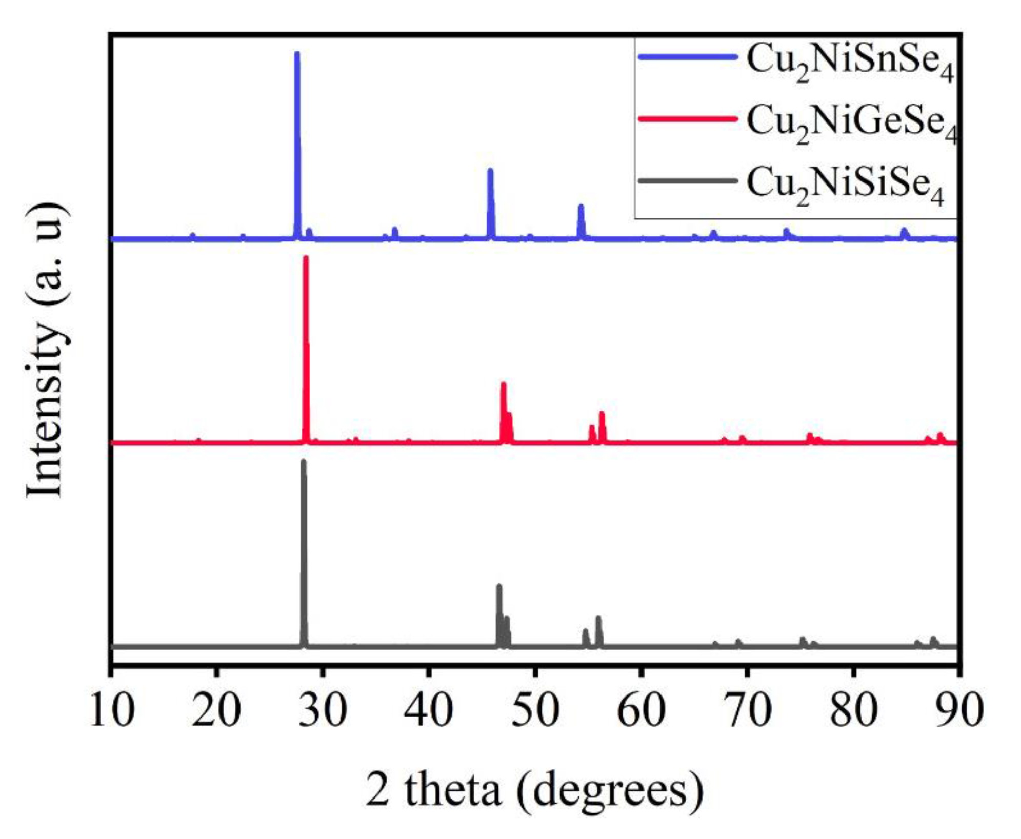
Figure 6.
Evolution of the band structure of Cu2Ni(Sn, Ge, Si)Se4 system and its impact on optimizing optoelectronic and photovoltaic properties.
Figure 6.
Evolution of the band structure of Cu2Ni(Sn, Ge, Si)Se4 system and its impact on optimizing optoelectronic and photovoltaic properties.
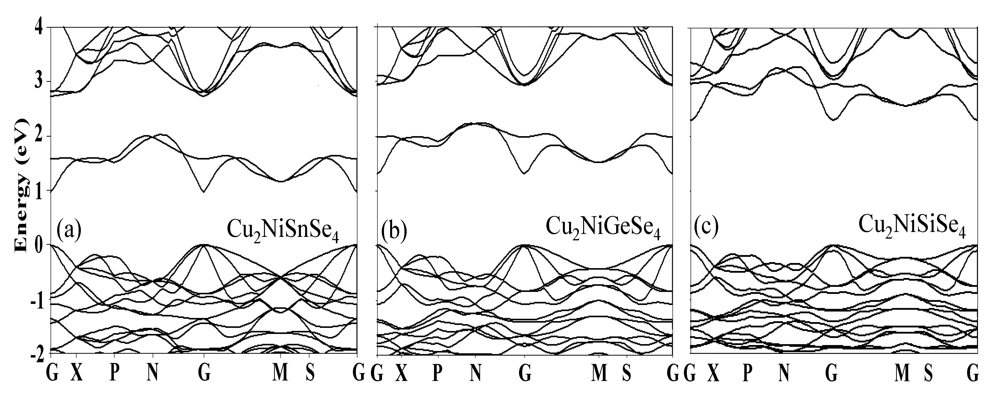
Figure 7.
Calculated values of the effective masses of electrons
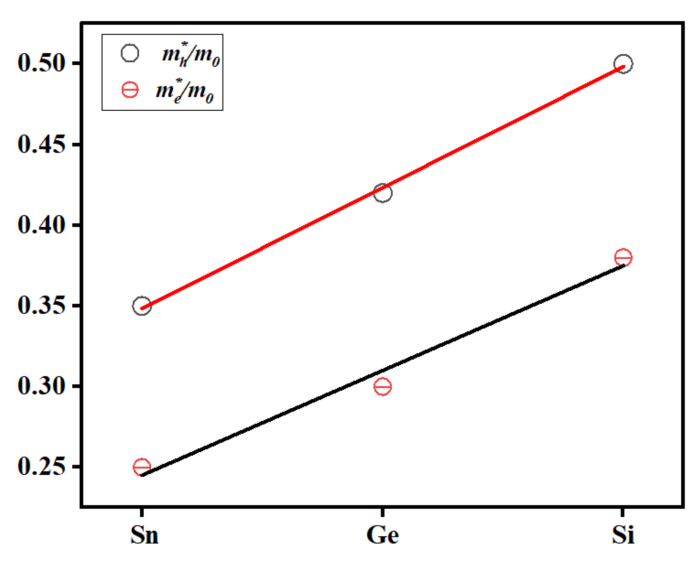
Figure 10.
Comparison of the partial density of states (PDOS) for Cu2Ni(Sn, Ge, Si)Se4 system in the valence band and conduction band.
Figure 10.
Comparison of the partial density of states (PDOS) for Cu2Ni(Sn, Ge, Si)Se4 system in the valence band and conduction band.
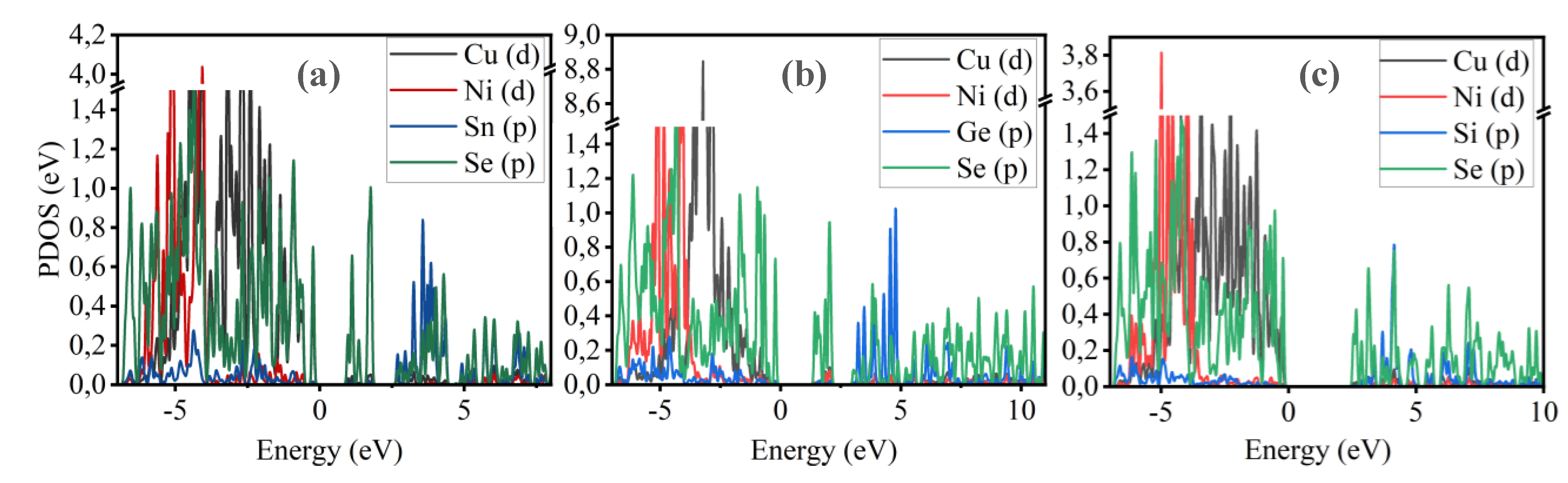
Figure 11.
Calculation of the total electronic density of states for: (a) Cu2NiSnSe4, (b) Cu2NiGeSe4, and (c) Cu2NiSiSe4, considering spin polarization (spin-up and spin-down).
Figure 11.
Calculation of the total electronic density of states for: (a) Cu2NiSnSe4, (b) Cu2NiGeSe4, and (c) Cu2NiSiSe4, considering spin polarization (spin-up and spin-down).
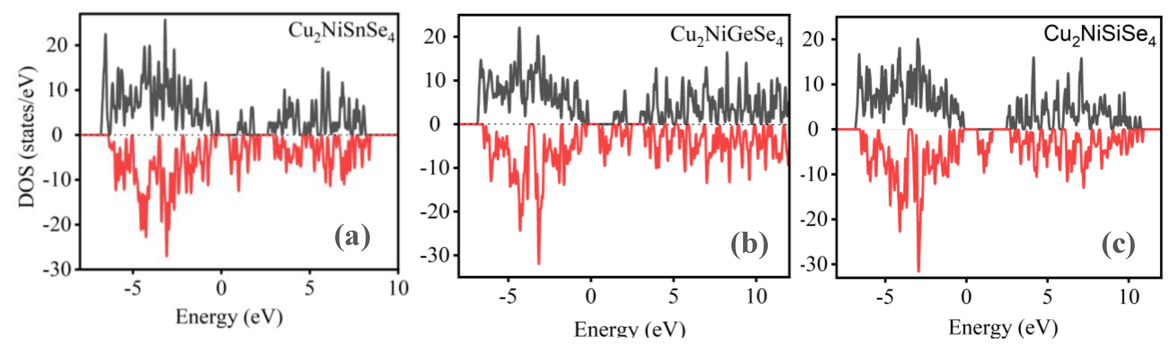

Table 1.
Comparison of lattice parameters for the Cu2Ni(Sn, Ge, Si)Se4 system obtained using various exchange-correlation functionals.
Table 1.
Comparison of lattice parameters for the Cu2Ni(Sn, Ge, Si)Se4 system obtained using various exchange-correlation functionals.
| SYSTEM | Lattice constants | PBE (GGA) | PBEsol | SCAN |
|---|---|---|---|---|
| Cu2NiSiSe4 | a, b (Å) | 5.491 | 5.373 | 5.406 |
| c (Å) | 11.044 | 10.911 | 11.048 | |
| α=β=γ, o | 90 | 90 | 90 | |
| V (Å3) | 333.060 | 315.034 | 322.983 | |
| Cu2NiGeSe4 | a, b (Å) | 5.54646 | 5.423 | 5.432 |
| c (Å) | 11.171 | 11.035 | 11.174 | |
| α=β=γ, o | 90 | 90 | 90 | |
| V (Å3) | 343.684 | 324.570 | 329.716 | |
| Cu2NiSnSe4 | a, b (Å) | 5.669 | 5.567 | 5.597 |
| c (Å) | 11.319 | 11.088 | 11.216 | |
| α=β=γ, o | 90 | 90 | 90 | |
| V (Å3) | 363.868 | 343.676 | 351.372 |
Table 2.
GGA-calculated total and formation energies for Cu2Ni(Sn,Ge,Si)Se4 compounds.
| System | Total Energy (eV) | Formation Energy (eV) |
|---|---|---|
| Cu2NiSnSe4 | -65.639 | -50.809 |
| Cu2NiGeSe4 | -66.628 | -51.638 |
| Cu2NiSiSe4 | -68.851 | -54.081 |
Table 3.
Comparison of the band gap values obtained using the mBJ and HSE06 potentials based on relaxed structures with GGA, PBE-sol, and SCAN functionals.
Table 3.
Comparison of the band gap values obtained using the mBJ and HSE06 potentials based on relaxed structures with GGA, PBE-sol, and SCAN functionals.
| SYSTEM | HSE06/GGA | HSE06/SCAN | HSE06/PBEsol | mBJ/GGA | mBJ/SCAN | mBJ/PBEsol |
|---|---|---|---|---|---|---|
| Cu2NiSnSe4 | 0,638 | 0,792 | 0,66 | 0,22 | 0,341 | 0,231 |
| Cu2NiGeSe4 | 0,968 | 1,232 | 1,078 | 0,539 | 0,726 | 0,572 |
| Cu2NiSiSe4 | 2,101 | 2,354 | 2,167 | 1,617 | 1,826 | 1,628 |
Table 4.
Calculated values of Fermi energy (EF) and effective masses of electrons/holes (in units of free electron mass, m0) for Cu2NiSnSe4, Cu2NiGeSe4 and Cu2NiSiSe4.
Table 4.
Calculated values of Fermi energy (EF) and effective masses of electrons/holes (in units of free electron mass, m0) for Cu2NiSnSe4, Cu2NiGeSe4 and Cu2NiSiSe4.
| SYSTEM | EF (eV) | |||
|---|---|---|---|---|
| Cu2NiSnSe4 | 5.12 | 0.35 | 0.25 | |
| Cu2NiGeSe4 | 5.07 | 0.42 | 0.30 | |
| Cu2NiSiSe4 | 5.16 | 0.50 | 0.38 |
Disclaimer/Publisher’s Note: The statements, opinions and data contained in all publications are solely those of the individual author(s) and contributor(s) and not of MDPI and/or the editor(s). MDPI and/or the editor(s) disclaim responsibility for any injury to people or property resulting from any ideas, methods, instructions or products referred to in the content. |
© 2025 by the authors. Licensee MDPI, Basel, Switzerland. This article is an open access article distributed under the terms and conditions of the Creative Commons Attribution (CC BY) license (http://creativecommons.org/licenses/by/4.0/).
Copyright: This open access article is published under a Creative Commons CC BY 4.0 license, which permit the free download, distribution, and reuse, provided that the author and preprint are cited in any reuse.


