
Submitted:
28 May 2025
Posted:
29 May 2025
You are already at the latest version
Abstract
Two-dimensional (2D) materials have emerged as promising candidates for next-generation photodetectors due to their atomically thin nature, strong light–matter interactions, mechanical flexibility, and tunable optoelectronic properties. This review presents recent advances in 2D material-based photodetectors, focusing on high-performance devices constructed from Graphene, Transition Metal Dichalcogenide (TMDC), Black phosphorus (BP), MXenes, bismuth and antimony chalcogenides, and tin chalcogenides. Key performance metrics such as responsivity, response speed, detectivity, and mechanical stability are discussed across different spectral regions. The performance, key characteristics, and recent achievements of each of the 2D photodetectors are described in detail. Despite these achievements, challenges such as scalability, stability, and interface engineering remain. This review concludes with insights into current limitations and outlines future directions for the design and development of flexible, high-efficiency, and broadband 2D photodetectors.
Keywords:
absorption
; photodetection
; 2D material
; responsivity
; surface plasmon
1. Introduction
Photodetectors (PDs) play a critical role in modern optoelectronic systems by converting incident electromagnetic radiation—spanning the ultraviolet (UV), visible, and infrared (IR) spectra—into electrical signals. These devices underpin a wide array of applications, including optical communication networks, environmental and industrial monitoring, chemical and biological sensing, imaging systems, and medical diagnostics. Traditionally, photodetectors have been fabricated using bulk semiconductors such as silicon (Si), indium gallium arsenide (InGaAs), and mercury cadmium telluride (HgCdTe), due to their well-characterized optoelectronic properties and compatibility with mature fabrication technologies [1]. However, these conventional materials are inherently constrained by several intrinsic limitations—most notably, fixed and relatively narrow bandgaps, limited doping tunability, and high susceptibility to thermal noise. These limitations collectively hinder the performance of conventional photodetectors in terms of responsivity, spectral tunability, and detection efficiency, especially under low-light or ambient operating conditions.
The emergence of two-dimensional (2D) materials has opened new frontiers in photodetector design and performance. Owing to their atomically thin structure and quantum confinement effects, 2D materials offer extraordinary physical and chemical properties that are highly advantageous for optoelectronic applications [2,3]. These include broadband optical absorption, ultrafast carrier dynamics, high carrier mobility, mechanical flexibility, and facile integration with diverse substrates. Notable examples of 2D materials with promising photodetection capabilities include graphene, transition metal dichalcogenides (TMDCs), black phosphorus (BP), hexagonal boron nitride (h-BN), and emerging III–V monolayers. Furthermore, vertical and lateral van der Waals (vdW) heterostructures—formed by stacking or patterning different 2D materials—enable novel functionalities that are unattainable in traditional bulk systems [4,5,6,7,8].
A particularly attractive feature of 2D materials is their compatibility with silicon-based platforms. Unlike bulk III–V semiconductors, which suffer from lattice and thermal expansion mismatches when integrated with silicon substrates, 2D materials can be transferred onto a variety of surfaces using vdW assembly techniques, eliminating the need for lattice matching [9,10]. This integration strategy offers a scalable pathway for the realization of high-performance, CMOS-compatible photonic systems, particularly for mid-infrared (MIR) and terahertz (THz) applications where conventional materials fall short [4].
This review provides a comprehensive overview of different 2D photodetectors and their various detection mechanisms, with a focus on their underlying physical principles and relevance to optoelectronic device performance. Specifically, we discuss key mechanisms including the photovoltaic effect, photothermoelectric effect, photoconductive response, bolometric effect, carrier generation and trapping, built-in electric fields in heterostructures, and plasmon-enhanced detection. Each mechanism is examined in the context of specific material properties and device architectures. By elucidating these photodetection pathways, this review aims to highlight the current advancements and future potential of 2D materials in enabling next-generation photodetectors for diverse spectral regimes and application domains.
2. Mechanisms of Photodetection in 2D Materials
Photodetection and other optoelectronic applications are fundamentally based on the conversion of absorbed photons into electrical signals. In 2D materials, this process can occur through various mechanisms, each offering unique advantages and operating principles. These mechanisms include the photovoltaic effect, the photo-thermoelectric effect, carrier generation and trapping effects, the bolometric effect, plasmon-enhanced photodetection, enhancement via localized surface plasmons, the photoconductive mechanism, and the photogating effect. The following sections provide a detailed discussion of these mechanisms, highlighting their underlying physics and potential applications [11].
2.1. Photovoltaic Effect
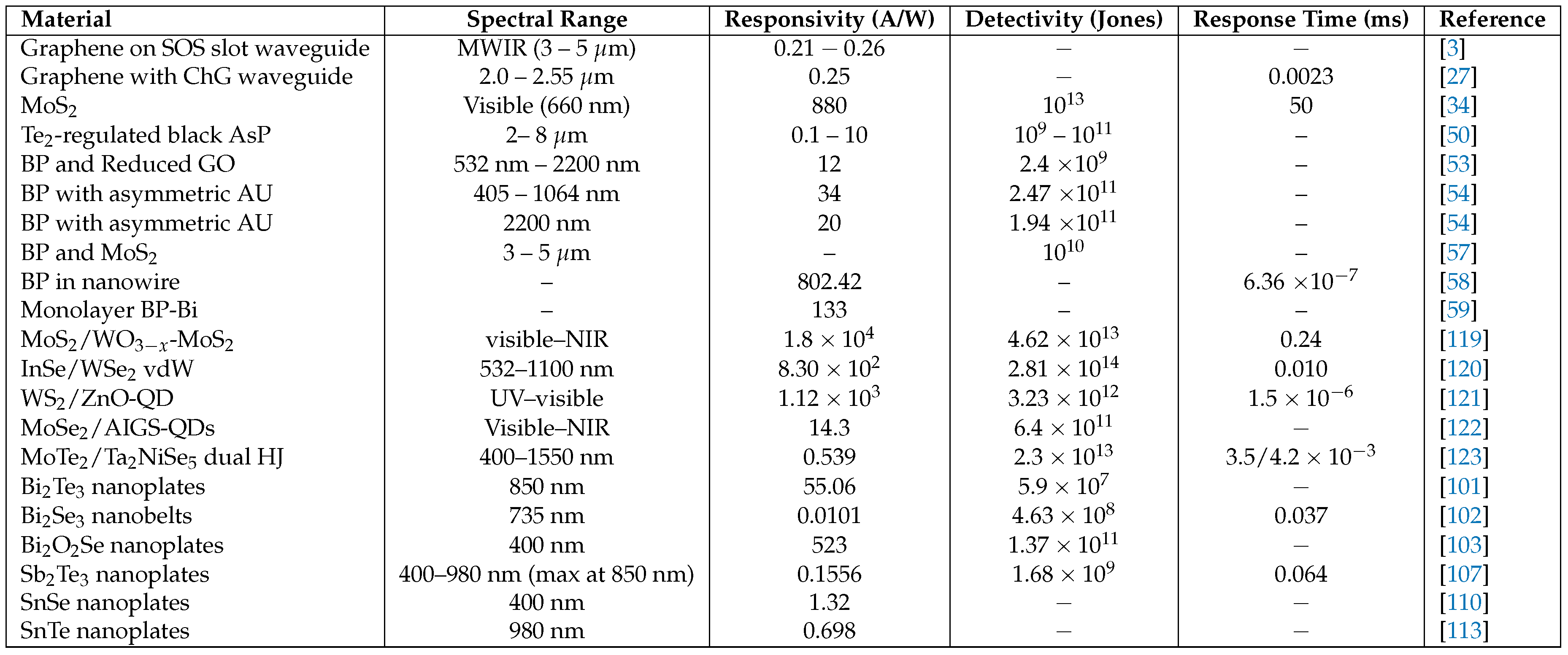
Photovoltaic effect arises from the separation of photogenerated charge carriers due to an internal electric field at the junction between n-type and p-type semiconductor regions [12]. Alternatively, an external electric field, induced by applying a bias voltage between the source and drain, can also drive this effect. However, this approach is less desirable as it introduces dark current, as illustrated in Figure 1(a) [13]. The intrinsic electric field can be established either by local chemical doping using split gates or through the work function difference between the active material and metal contacts [14]. The resulting photocurrent aligns with the electric field direction and remains independent of the doping concentration. Consequently, a polarity shift in current flow is observed between pn and np junctions. Additionally, carrier multiplication, driven by electron-electron scattering, facilitates the conversion of high-energy electron-hole pairs into multiple lower-energy pairs, enhancing photodetection efficiency [15].
2.2. Photothermoelectric Effect
Photovoltaic effect occurs when light-induced temperature gradients within a material generate an electric voltage via the Seebeck effect, facilitating light detection based on thermal variations. This phenomenon, known as the photo-thermoelectric effect [16], involves the indirect conversion of light into electrical signals due to spatial differences in light absorption. As a result, electron thermal motion within the active region induces a temperature gradient, as illustrated in Figure 1(b) [13]. According to the Seebeck effect, this temperature difference alters the electronic properties of the material, leading to a measurable potential difference [17]. The induced photo-thermoelectric voltage, expressed as , depends on the thermoelectric coefficients of the material ( and ) and the temperature gradient T across different regions. The magnitude of these coefficients is closely linked to the material’s conductance [17].
2.3. Photoconductive Mechanism
The photoconductive effect occurs when the absorption of light enhances the electrical conductivity of a semiconductor. Incident photons excite electrons from the valence band to the conduction band, generating electron-hole pairs and increasing the charge carrier density (see Figure 1 (c) [2]. Under an applied electric field, these free carriers contribute to a measurable photocurrent. Unlike photovoltaic devices, which operate at zero bias, photoconductive devices require an external electric field to facilitate charge transport and photocurrent generation [14]. Additionally, carrier recombination may occur, affecting the efficiency of the process.
2.4. Bolometric Effect
The bolometric effect in photodetectors refers to the variation in electrical resistance of a material due to temperature changes induced by incident electromagnetic radiation. This effect is leveraged in bolometric photodetectors, where absorbed light energy is converted into an electrical signal [18]. As shown in Figure 1(d), when light is absorbed, the resulting temperature increase alters the material’s resistivity, leading to a photocurrent that scales with the applied voltage [13]. This resistivity change occurs through two primary mechanisms: (1) a temperature-dependent variation in carrier mobility and (2) a change in carrier contribution to the current. The sensitivity and response time of bolometric devices are primarily influenced by the material’s thermal resistance () and heat capacity () [18].
2.5. Carrier generation and trapping effects
Upon light absorption, electron-hole pairs are generated. However, defects or impurities in the material can trap these carriers, prolonging their lifetime and affecting the photodetector’s response time and sensitivity.
2.6. Built-in electric field in heterostructures
At the interface of different 2D materials forming a heterostructure, differences in work functions and band alignments create an internal electric field. This field facilitates efficient separation and transport of photogenerated carriers, enhancing photodetector performance [19].
2.7. Plasmon-Enhanced 2D hetrostrucutres
Localized surface plasmons (LSPs) and surface plasmon polaritons (SPPs) are collective oscillations of electrons on the surface of metallic nanostructures excited by light. These oscillations amplify the local electromagnetic field, boosting light-matter interactions and enhancing the performance of 2D photodetectors.As a result, integrating plasmonic nanostructures with 2D materials can concentrate light into sub-wavelength volumes, enhancing local electromagnetic fields and thereby increasing light absorption and photocurrent generation in photodetectors. Hence, 2D materials such as graphene and transition metal dichalcogine (TMDC) monolayers exhibit low light absorption due to their atomically thin structure, limiting their efficiency in converting light into electrical signals. As a result, hybridizing these materials with plasmonic nanostrucutres is essential for enhancing the perfomance of photodetectors. For example, Yuan Liu et al. demonstrated the feasibility of pristine graphene as compared to integration with gold nanostrucures. Although pristine graphene photodetectors are ultra-fast and broadband, they suffer very low quantum efficiency ( 0.1–0.2%). By integrating plasmonic gold nanostrucutres onto graphene, a drastic photocurrent enhancement of up to 1500% was achieved, enabling multicolour photodetection [20].
3. 2D Materials for Photodetection
In recent years, the exploration of 2D materials has led to significant breakthroughs in the development of high-performance photodetectors. Due to their atomically thin nature, tunable bandgaps, and strong light–matter interaction, 2D materials offer a versatile platform for designing photodetectors across a broad spectral range: from ultraviolet to far infrared. This section provides a comprehensive overview of various classes of 2D materials that have demonstrated strong potential for photodetection applications.
3.1. Graphene-Based Photodetectors
In the Mid-infrared (MIR) region, graphene has been successfully integrated into the Si substrate which has demonstrated superior performance compared to 2-D black phosphorus (BP) [5] which suffers from surface instability due to chemical degradation [6], limiting its practicality for on-chip sensing applications. Graphene being a gapless semiconductor that is capable of detecting electromagnetic radiation from the far infrared to the ultraviolet [21]. Researchers have reported on-chip MIR graphene photodetectors [7,22,23,24,25,26,27]. Wang et al. reported the development of a graphene/silicon heterojunction photodetector by integrating a graphene layer onto a silicon optical waveguide fabricated on a silicon-on-insulator (SOI) platform. This configuration enabled the efficient absorption of evanescent light traveling parallel to the graphene surface, allowing the device to operate effectively across the near- to mid-infrared spectrum. At a bias voltage of 1.5 V, the photodiode demonstrated a responsivity of 0.13 A/W for incident light with a wavelength of 2.75 m at room temperature [23]. In a related work, Cheng et al. fabricated heterostructure waveguide photodetectors by transferring chemical vapor deposition (CVD) grown graphene onto silicon-on-sapphire (SOS) waveguides. These devices exhibited responsivities of 0.9 mA/W at 1.55 m and 4.5 mA/W at 2.75 m, highlighting the potential of graphene-based integration for broadband infrared photodetection [22].
Lin et al. presented an efficient approach for fabricating graphene-based photodetectors by directly depositing and patterning chalcogenide glass (ChG) waveguides and metal electrodes onto monolayer graphene synthesized via chemical vapor deposition (CVD), thereby simplifying the integration of the photodetector with the optical waveguide system (Figure 2(a), inset) [27]. To assess the device’s performance, mid-infrared light with transverse electric (TE) polarization was launched into the waveguide, and the generated photocurrent was recorded under zero-bias conditions (Figure 2(b)). Graphene’s photoresponse typically arises from a combination of three fundamental mechanisms: the photothermoelectric effect, the photovoltaic (PV) effect, and the bolometric effect. To determine which of these played the dominant role in the observed photocurrent, the authors compared experimental results against theoretical models for each mechanism. Among the three, the photovoltaic effect model exhibited the best agreement with the measured data (Figure 2(c)). From the fitting, a hot carrier relaxation time of 2.3 picoseconds was extracted, which is consistent with values reported in earlier studies [28,29]. Additionally, the responsivity of the device was found to increase with applied bias voltage, attributed to improved efficiency in charge carrier collection. An asymmetry in the photocurrent response curve was observed, which the authors linked to the lateral displacement of the waveguide relative to the graphene channel (Figure 2(a)). Deviations from the photovoltaic model at negative biases exceeding -1 V were likely a result of the intrinsic disparity in electron and hole mobilities in graphene [30]. The photodetector exhibited broadband sensitivity throughout the entire tuning range of the laser source (2.0 - 2.55 m ), achieving a peak responsivity of 250 mA/W at a wavelength of 2.03 m (Figure 2(d)). This level of performance is competitive with, and in some instances surpasses, other state-of-the-art waveguide-integrated graphene photodetectors developed for both mid-infrared [31] and near-infrared applications [32,33]. Notably, achieving responsivities above 10 mA/W in the mid-infrared (MIR) range remains a significant challenge for graphene-based detectors.
In a related advancement, Mohammed Alaloul and colleagues proposed a mid-wave infrared (MWIR) graphene photodetector integrated with silicon-on-sapphire slot waveguides, optimized for on-chip gas sensing through absorption spectroscopy (Figs. Figure 2(e) and Figure 2(f)). The device capitalizes on the strong interaction between the optical mode and analyte gases in the slotted air region of the waveguide, which is crucial for high-sensitivity detection. The authors evaluated the device by analyzing its current responsivity () and detection capabilities for trace gases such as carbon dioxide (CO2), methane (CH4), and nitrous oxide (N2O). As shown in Figure 2(g), the across the MWIR band remained relatively uniform, ranging between 0.21 and 0.26 A/W. Minor fluctuations in the were attributed to variations in coupling efficiency and wavelength-dependent absorption by graphene in the waveguide-integrated setup. The obtained responsivity is much greater than previously reported MIR graphene-based photodetectors [31,32,33], which is critical to enhance the sensitivity of the device in detecting low concentrations of target gases. Impressively, the system demonstrated the ability to detect minimum concentrations () as low as 0.14 parts per billion (ppb) for CO2, 0.52 ppb for N2O, and 0.72 ppb for CH4 under a source power of 2 mW (Figure 2(h)) [3].
3.2. Transition Metal Dichalcogenides Photodetectors
Two-dimensional transition metal dichalcogenide (TMDC) monolayers such as molybdenum disulfide (MoS2), tungsten disulfide (WS2), tungsten diselenide (WSe2), molybdenum diselenide (MoSe2), and molybdenum ditelluride (MoTe2) exhibits direct bandgap semiconductor characteristics in the visible to near-infrared spectrum when reduced to a single atomic layer [34,35]. Their intrinsic properties including direct bandgaps in the range of 1.1 to 2.1 eV, high exciton binding energies (>300 meV), strong light–matter interaction, and mechanical flexibility have enabled device innovations with extraordinary responsivity, detectivity, and tunability. When these TMDCs are operated in photovoltaic mode, a built-in electric field at a junction (e.g., TMDC p–n junction or Schottky barrier) separates electrons and holes, generating photocurrent even under very low bias. Such TMDC photodiodes typically offer faster, low-noise operation due to suppressed dark current, though they generally exhibit lower gain compared to phototransistors. Figure 3a–b illustrates a representative device structure where monolayer MoS2 is integrated on a silicon nitride waveguide: under lateral evanescent illumination, electron–hole pairs generated in the MoS2 are collected by biasing the channel, thereby converting guided light into electrical signals [36]. As a result, coupling light laterally via a waveguide significantly enhances absorption in the atomically thin monolayer compared to normal incidence, effectively approaching unity absorption for sufficiently long interaction lengths (Figure 3c). The versatility of TMDCs is also evident in configurations ranging from monolayers to vertically stacked heterostructures. For instance, Wang et al. demonstrated a vertically stacked 2H-MoS2/1T@2H-MoS2 heterojunction that achieves a responsivity of 1917 A/W and detectivity on the order of 1011 Jones through phase-engineered internal junctions and bias modulation [37]. As shown in Figure 3d–e, the 1T metallic phase in the heterostructure facilitates efficient carrier transport, while the 2H semiconducting phase enables light absorption, demonstrating how phase engineering can optimize performance and achieve high responsivity. On the other hand, forming van der Waals heterojunctions is a key strategy to achieve both high responsivity and fast response. For instance, Gherabli et al. demonstrated a lateral p–n heterojunction between p-type MoSe2 and n-type WS2 monolayers integrated on a silicon nitride (SiN) waveguide, resulting in a self-driven photodiode with ultra-low dark current (∼50 pA) and a peak responsivity of approximately 0.9 A/W at 780 nm [38]. As shown in Figure 3f–g, the MoSe2–WS2 photodetector exhibits strong optical field confinement when coupled with the waveguide, significantly enhancing light absorption within the TMDC region. Consequently, as illustrated in Figure 3g, the device demonstrates a temporal photoresponse with a dB bandwidth of ∼20 MHz and sub-30 ns rise and fall times, confirming its potential for high-speed on-chip applications.
Other TMDCs, such as WSe2, MoSe2, and MoTe2, have also enabled diverse device architectures and photonic enhancements. For instance, Singla et al. demonstrated a significant enhancement in the broadband photoresponse of a MoTe2/MoS2 bilayer photodetector by integrating it with hyperbolic metamaterial (HMM) nanocavities. This integration led to an 8-fold increase in photocurrent under on-resonance conditions and a 2.5-fold increase off-resonance (see Figure 1(h–j)). This enhancement is attributed to the localized electric fields around each nanocavity, which intensify light–matter interactions within the 2D materials [39]. Doping strategies have also yielded transformative performance gains. Kang et al. investigated the impact of self-assembled monolayer (SAM) doping on the performance of WSe2- and MoS2-based photodetectors. By employing octadecyltrichlorosilane (OTS) for p-doping WSe2 and aminopropyltriethoxysilane (APTES) for n-doping MoS2, they achieved significant enhancements in device performance. Specifically, the responsivity of WSe2 photodetectors increased from 517.2 A/W to A/W, and that of MoS2 devices improved from 219 A/W to A/W, representing approximately 28-fold and 26-fold enhancements, respectively [40]. These improvements were attributed to the non-destructive nature of SAM doping, which effectively modulates the carrier concentration without impairing carrier transport properties. This approach demonstrates a promising strategy for dynamically tuning the optoelectronic properties of two-dimensional materials for advanced photodetector applications. Furthermore, TMDC monolayers offer several key advantages over other 2D-material-based photodetectors. Graphene, though extensively studied for photodetection, suffers from fundamental limitations due to its zero bandgap and semimetallic nature. While graphene photodetectors are known for their ultrabroadband spectral coverage and ultrafast response, they typically exhibit high dark current and low intrinsic responsivity owing to minimal optical absorption and the absence of photogain without additional enhancement structures [41]. In contrast, TMDC monolayers possess sizable and tunable direct bandgaps in the visible to near-infrared (NIR) range, along with strong excitonic absorption, leading to significantly lower off-state currents and inherently higher photoresponsivity. Graphene’s light absorption, approximately 2.3% per layer is notably lower than that of TMDCs, which can exhibit an order of magnitude greater absorption at excitonic resonances [41]. As a result, TMDC-based photodetectors often achieve superior signal-to-noise ratios. For instance, monolayer MoS2 phototransistors can reach responsivities at the A/W level without requiring optical cavities or plasmonic structures, which are typically necessary in graphene-based devices to achieve even mA/W performance. While graphene excels in speed, with bandwidths exceeding tens of GHz, TMDCs also support high-speed operation; recent p–n junction devices have demonstrated bandwidths above 30 GHz, making them suitable for high-speed optoelectronic applications across the visible spectrum [42]. Moreover, TMDC-based photodetectors are also more stable than their black phosphorus (BP) counterparts. Despite BP offering a tunable mid-IR bandgap and high mobility, it is chemically unstable under ambient conditions [43].
The unique combination of high sensitivity and integrability makes TMDC photodetectors attractive for a broad range of technological applications. For instance, two recent studies have demonstrated the potential of MoS2-based active pixel sensor (APS) arrays for next-generation imaging. Dodda et al. developed a monolayer MoS2 phototransistor array that integrates image capture and in-sensor processing within a compact, low-power platform (<1 pJ/pixel), achieving ultra-high responsivity (∼3.6 × 10⁷ A/W), detectivity (∼5.6 × 10¹³ Jones), and dynamic range (∼80 dB) using gate-tunable persistent photoconductivity. Their approach eliminates the need for peripheral circuitry for analog de-noising and reset, making it ideal for edge computing in IoT systems [44]. Additionally, Hong et al. fabricated a large-area bilayer MoS2 APS using a transfer-free growth method, achieving responsivity up to 119 A/W and demonstrating high pixel uniformity and signal-to-noise ratio [45]. They attributed this enhancement to photogating via hole trapping at subgap states, confirmed through simulation and spectroscopic analysis. Together, these works highlight the feasibility of scalable, high-performance, and energy-efficient TMDC-based imaging platforms. Due to their atomic thickness, TMDCs can be vertically stacked or tiled on focal plane arrays without adding significant bulk, facilitating multispectral imaging through the use of different TMDC materials tuned to distinct spectral bands. Moreover, TMDC photodetectors are increasingly used as in-situ optical read-heads in chemical and biological sensing. For example, Park et al. developed a 4 × 4 mini-array of few-layer MoS2 integrated with microfluidic enzyme chambers to detect the blood biomarker D-lactate in 2.5 L samples within 10 minutes, achieving sub-g mL−1 sensitivity due to high responsivity and pixel uniformity [46].
Photodetectors based on thin TMDCs combine direct bandgap semiconducting behavior, strong optical absorption, and atomic-scale thickness to deliver high responsivity, low dark current, and easy integration onto rigid, flexible, or photonic platforms. Over the past decade, they have advanced from lab-scale flakes to wafer-level arrays. Monolayer MoS2 phototransistors now reach responsivities beyond 106 A/W; WSe2 and MoTe2 p–n diodes offer low dark current and multi-gigahertz bandwidths suitable for telecom applications; and hybrid structures integrate sensing, memory, and processing at the pixel level [44,45]. As a result, TMDC photodetectors offer many advantages, especially in terms of flexibility and system-level integration. Further progress depends on innovations in materials and device engineering. Optimized contacts such as edge-engineered metals or 2D conductors—could reduce series resistance and noise. Doping strategies, whether chemical or electrostatic, can tune spectral response while preserving carrier mobility. Heterostructures combining TMDCs with black phosphorus, perovskites, quantum dots, or plasmonic resonators offer enhanced gain, broader spectral range, and multifunctionality. In particular, integrating TMDC monolayers with ultrathin plasmonic metamaterials can induce strong local electric field enhancements [47,48], significantly increasing optical absorption and overall photodetector performance. Techniques such as strain engineering and the use of high- dielectrics can further improve carrier dynamics and reduce flicker noise. Scalable, transfer-free growth on CMOS-compatible substrates remains key to industrial adoption. These strategies will enable TMDC photodetectors with high speed, sensitivity, and mechanical adaptability for future imaging, communication, and wearable sensing systems.
3.3. Black Phosphorus (BP) Photodetectors
Black phosphorus (BP), a layered 2D semiconductor with a tunable bandgap ranging from 0.3 eV (bulk) to ≈ 2 eV (monolayer), has emerged as a leading candidate for broadband photodetection, particularly in the infrared (IR) and midwave infrared (MWIR) spectral ranges [49]. Its anisotropic carrier mobility, high absorption coefficient, and out-of-plane electric field response provide unique advantages over traditional semiconductors and even other 2D materials [49]. Recent work has focused on enhancing the material’s optoelectronic response, air stability, and spectral tunability, positioning BP as a key enabler for next-generation photodetectors.
Several studies have focused on improving synthesis and processing of BP for device fabrication. Song et al. demonstrated uniform, large-area Te2-regulated black arsenic phosphorus films that achieved remarkable self-powered IR detection with detectivity up to Jones [50]. Similarly, Wan et al. developed a chemical vapor transport method to grow wafer scale BP, enabling memristive behavior and neuromorphic functions in optoelectronic systems [51]. These fabrication strategies are critical for transitioning BP-based photodetectors from the lab to scalable technologies. To overcome BP’s environmental instability, multiple chemical and physical passivation techniques have been reviewed. Zhang et al. comprehensively discussed encapsulation and doping strategies that significantly reduce photo-oxidation, extending device lifetimes in ambient conditions [52]. Integration with stable materials has also been proven to be effective. Zhou et al. fabricated solution-processed BP/RGO Schottky junctions that operate temperatures up to 400 K while maintaining near-IR responsiveness up to 2200 nm [53]. Device engineering has played a crucial role in enhancing performance metrics like responsivity, response time, and spectral coverage. Shen and Hou developed asymmetric Schottky BP transistors achieving detectivity as high as Jones in the 400–2200 nm range [54]. Advanced designs such as twisted bilayers (Chen et al., 2024) introduced tunable photoluminescence and the bulk photovoltaic effect, offering new pathways to manipulate carrier dynamics without external bias [55]. Heterostructure-based devices have seen significant advancements. Hu and team engineered heterogeneous Z/S scheme BP interfaces to enhance interfacial charge transfer, boosting photogenerated carrier separation efficiency [56]. Likewise, BP-MoS2 diodes, integrated with metasurfaces, demonstrated superior MWIR absorption in the 3–5 m range (Lien et al., 2023) [57]. These vertical and lateral heterojunctions significantly enhance optical gain and offer spectral selectivity.
Polarization sensitivity and directionality are also intrinsic to BP’s anisotropic nature. Hao and co-workers fabricated a Dember effect based anisotropic photodetector with polarization ratios exceeding 100, suggesting potential use in imaging and sensing applications [58]. Similarly, Li et al. explored ferroelectric black bismuth (a BP analog) showing asymmetric photocurrent generation under zero bias due to intrinsic photogalvanic effects [59]. To improve spectral reach, several studies have employed metamaterials and waveguide integrations. Graphene/BP metasurface detectors developed by Ogawa et al. utilized localized surface plasmon resonance to modulate IR absorption characteristics [60], while Wang and co-wokers demonstrated that the BP integrated with lithium niobate photonic waveguides that showed 100 ns responses in the telecom range [61]. These hybrid devices highlight the compatibility of BP with photonic circuitry and IR fiber optic communication platforms. Mid-infrared operability and high-temperature resilience are also emerging themes. Yang et al. designed BP/PtSe2 Schottky devices capable of maintaining high responsivity (≈ 25 A/W) up to 470 K, demonstrating BP’s viability in harsh environments [62]. BP’s performance in MWIR surpasses that of commercial III-V photodetectors in room-temperature conditions, as reviewed by Higashitarumizu et al. [63]. Meanwhile, Zhu et al. emphasized the importance of BP’s layer dependent tunability and multi type architecture versatility in their extensive review [64]. Also in Figure 4 (a) and (c) show the different architectures of device fabrication.
Collectively, these works highlight that black phosphorus, with its unique band structure and anisotropy, stands at the forefront of 2D infrared optoelectronics. Yet challenges remain, including intrinsic air sensitivity, reproducibility in large scale synthesis, and integration with CMOS-compatible platforms. The field is now rapidly moving toward hybrid and multifunctional device architectures where BP serves as the active layer alongside plasmonic, ferroelectric, and metamaterial components.
3.4. MXenes Photodetectors
Two-dimensional (2D) MXenes have emerged as highly promising materials for photodetector applications, owing to their unique electronic and optical properties. As members of the transition metal carbides and nitrides family, MXenes exhibit high electrical conductivity, tunable work functions, and excellent optoelectronic characteristics [67]. These features have driven extensive research into integrating MXenes with various semiconductors and nanostructures, aiming to enhance the performance of photodetectors. This overview highlights recent advancements in 2D MXene photodetectors, focusing on material innovations, device architectures, and key performance metrics.
A major focus in MXene-based photodetectors has been the development of heterojunctions and composite structures to improve charge separation and light absorption. For example, the integration of MXene with bismuth vanadate (BiVO4) forms a Schottky junction that significantly enhances photocurrent density and responsivity under visible light illumination [67]. Similarly, Ding et al. demonstrated that van der Waals MXene/gallium nitride (GaN) heterojunctions have high responsivity and operational stability in ultraviolet detection [68]. Rhyu et al. synthesized composite materials, such as MXene decorated with indium oxide (In2O3) nanoparticles, through sonochemical methods to achieve broadband responsivity spanning ultraviolet, visible, and near-infrared wavelengths. These composites enable flexible photodetectors that maintain high responsivity and mechanical robustness under bending or stretching [69]. High-entropy (HE) MXenes, such as TiVCrMoC3, represent another material innovation, exhibiting superior nonlinear optical properties and ultrafast photoresponse compared to conventional MXenes [70]. Gao and co-workers demonstrated that their stronger saturable absorption makes them suitable for applications in mode-locked lasers and ultrafast photodetection systems. Additionally, surface modifications and functionalization strategies have been employed to tailor MXene properties [70]. For instance, phenylsulfonic acid functionalization can open the bandgap of MXenes, allowing near-infrared photodetection and enabling the fabrication of flexible photodetectors with high responsivity and detectivity [71].
MXene-based photodetectors have demonstrated impressive performance metrics, including high responsivity and detectivity across different wavelength ranges. zhang et el. reported that MXene/germanium (Ge) Schottky heterostructures exhibited high responsivity as high as 665 mA/W and detectivity of Jones at 1550 nm, making them suitable for telecommunications applications [72]. Ghosh and Giri found that MXene/bismuth sulfide (Bi2S3) composites exhibited peak responsivities of 36.7 A/W in the UV range and 26.2 A/W in the near-infrared, demonstrating broadband detection capabilities [73]. li et al. explored that MXene/aluminum gallium nitride (AlGaN) van der Waals junctions achieve a responsivity of 101.85 mA/W Under deep ultraviolet illumination which shows their applicability in UV photodetection [74]. Fast response times and device stability are crucial for practical applications. Ding in el. reported that the rise and decay time of MXene/GaN photodetectors were 8 ms and 14 ms, respectively [68], while MXene/Ge heterostructures exhibit ultrafast response speeds of 1.4 s (rise) and 4.1 s (decay) [75]. Stability tests conducted by Zheng and co-workers revealed that MXene/ZnO nanorod photodetectors retain their electrical and optical properties even after 10,000 bending cycles, highlighting their potential for flexible and wearable devices [76]. Broadband and polarization-sensitive detection are additional key features of MXene photodetectors. For example, MXene/bismuth selenide (Bi2Se3) heterostructures constructed by Nandi et al. detected light throughout a broad spectral range of 300–2000 nm with a responsivity of 7.56 A/W at 980 nm [77]. Furthermore, Nb2-based photodetectors have demonstrated polarization sensitivity with an extinction ratio of 7.6, making them promising candidates for polarization sensitive applications such as optical communication and imaging [78].
Despite their promising features, MXene photodetectors face several challenges. The intrinsic metallic conductivity of MXenes can limit their use in photodetectors, which often require semiconducting behavior for efficient photoresponse [79]. Scalability and manufacturing remain difficult due to the need for precise control over material quality and interface engineering during large-scale synthesis and device fabrication [79]. Additionally, interfacial defects in heterojunctions can hinder charge transport and increase recombination, reducing device efficiency [72].The detailed results of the experiment conducted by Zhang and co-workers are shown in Figure 5 (a) to (k) [72]. However, MXenes also present significant opportunities. Their tunable work function allows optimization of heterojunctions for specific photodetection applications [80]. Their inherent mechanical flexibility makes them ideal candidates for flexible and stretchable optoelectronic devices, expanding the potential for wearable technologies [71,81]. Furthermore, emerging materials such as high-entropy MXenes and functionalized MXene derivatives open new avenues for improving photodetection performance and expanding the functional range of these devices [70,71]. Overall, 2D MXenes represent a versatile and powerful class of materials for next-generation photodetectors, with ongoing research continuing to address current challenges and unlock their full potential.
3.5. Carbide Photodetectors
Carbide-based photodetectors have gained significant traction in optoelectronics due to their exceptional material properties, including wide bandgap, thermal stability, and chemical inertness [82]. Among these, silicon carbide (SiC) is one of the most widely studied materials for ultraviolet (UV) detection [83,84]. Zhang et al. demonstrated that N-doped 4H-SiC photodetectors exhibit enhanced UV response due to a pyrophototronic effect that amplifies the photocurrent under transient conditions [82]. Ali et al. explored multiphoton photocurrent generation in SiC and found that even though the photon energy was below the bandgap, four photon absorption dominated the photocurrent at 1030 nm femtosecond excitation [85]. In another study, Koller et al. investigated strain-enabled control of vanadium spin qudits in SiC, suggesting the material’s potential for quantum photonics and spin-based sensing applications [86].
Researchers have also focused on heterostructures involving transition metal carbides and SiC to enhance photodetector performance. Abdo et al. reported that integrating a TaC:Cu alloy with 4H-SiC significantly improved near-UV responsivity at 405 nm, achieving a high photoresponsivity of 1.66 A/W [87]. Similarly, Akter et al. designed a high-performance Mo2C/SiC heterostructure that delivered efficient UV detection, with improved specific detectivity and signal stability [88] . Vanadium carbide (V2C), a MXene, was employed by Altaleb et al. to construct a mid-infrared (mid-IR) photodetector, achieving a responsivity of 2.65 A/W at 2 m and demonstrating compatibility with on-chip photonic circuits [89]. From a theoretical standpoint, Roy et al. performed first-principles simulations of quantum dots (QDs) composed of SiC and GeC, showing spin split energy states, SWIR emission, and enhanced gas sensing due to strong charge localization at heterojunctions [90]. Such theoretical insights were complemented by experimental studies. For example, Remeš et al. fabricated thin hydrogenated amorphous SiC films embedded with Ge nanocrystals and observed increased optical absorption in the near-infrared region, though with some degradation after high-temperature annealing [91].
Hybrid structures combining SiC with borides and organic materials have also been developed to expand photodetection capabilities. Hattori et al. demonstrated that a SiC-TaB2 heterostructure enables significant near-UV photoresponse [92] , while Akter et al. fabricated a deep-UV photodetector using zirconium diboride (ZrB2) and n-doped SiC, achieving performance suitable for high-temperature environments [93]. In the domain of organic-inorganic hybrids, Hattori et al. developed a device based on carbazole blended with 4H-SiC, (see Figure 6) which exhibited broad spectral sensitivity and enhanced responsivity [94]. These hybrid approaches address the limitations of individual materials by synergizing their optical and electronic properties. Graphene and other 2D materials have also been integrated with carbides to exploit their tunable electronic properties. Alaloul et al. developed a mid-infrared graphene photodetector on a SiC platform with high responsivity for gas sensing applications [3]. Yang et al. engineered an all-optical modulator based on a CdS/Graphene/Ge sandwich, demonstrating responsivity tunability from −3376 A/W to +3584 A/W, making it suitable for neuromorphic computing [95]. Additionally, Zhang et al. and Du et al. reviewed photodetectors based on graphitic carbon nitride and highlighted its advantages in flexible, broadband, and cost-effective detection platforms [96,97].
A variety of fabrication methods and device architectures have been employed to further improve performance. Lionas et al. compared solution-processed and chemical vapor deposited multi-wall carbon nanotube devices on Si3N4/n-Si, finding that UV sensitivity was superior in solution-processed devices [98]. Cai et al. used femtosecond laser pulses to probe nonlinear photocurrent effects in SiC, confirming the material’s robustness and suitability for high-power optical applications [99]. Zhang et al. showed that pyro-phototronic SiC photodetectors could perform imaging and signal modulation at room temperature [82]. Meanwhile, Woo et al. reported high detectivity dual-band infrared photodetectors based on dislocation-assisted gain mechanisms using heteroepitaxial layers involving carbide interfaces, expanding the utility of such devices to mid-IR applications [100]. In summary, recent advances underscore the versatility of carbide-based photodetectors. Their performance can be significantly enhanced through heterostructure engineering, organic and boride integration, and quantum-level modifications. These devices offer high responsivity across UV to mid-IR ranges, improved detectivity, thermal stability, and potential integration into flexible and neuromorphic platforms. Collectively, these findings position carbide photodetectors as leading candidates for next-generation sensing technologies in harsh and multifunctional environments.
3.6. Bismuth Chalcogenide Photodetectors
In the visible to near-infrared (NIR) wavelength range, bismuth chalcogenide nanomaterials have emerged as promising candidates for photodetection applications due to their unique properties. Bi2Te3 nanoplates grown by controlled chemical vapor deposition (CVD) have shown excellent photoresponse for visible light detection, exhibiting high responsivity of 55.06 A/W and specific detectivity of Jones at 850 nm [101]. Wang et al. reported that these devices demonstrated stable photoswitching behavior and maintained good performance after mechanical bending, indicating potential applications in flexible optoelectronics. Similarly, Liu et al. developed ultra-fast and high flexibility NIR photodetectors based on Bi2Se3 nanobelts grown via catalyst-free van der Waals epitaxy [102]. These devices achieved a rapid photoresponse (response time of 37 s and decay time of 62 s) with a responsivity of 10.1 mA/W and detectivity of Jones at 735 nm. More recently, Wang et al. fabricated broadband photodetectors based on Bi2O2Se nanoplates grown using chemical vapor deposition [103]. These square-shaped Bi2O2Se nanoplates showed exceptional performance at 77 K with a high responsivity of 523 A/W, specific detectivity of Jones, and external quantum efficiency of 162,119.44% under 400 nm illumination. Furthermore, the Bi2O2Se nanoplates enabled high-quality full-color imaging in the visible spectrum, highlighting their potential for advanced optoelectronic applications.
3.7. Antimony Chalcogenide Photodetectors
Similar to bismuth chalcogenides, antimony telluride (Sb2Te3) possesses a rhombohedral crystal structure with quintuple layers stacked by van der Waals interactions [104]. This structure, combined with its narrow bandgap ( eV) and high carrier mobility (200 ) [105,106], makes Sb2Te3 nanoplates promising for photodetection applications. Zhang et al. recently demonstrated high-performance photodetectors based on CVD-grown Sb2Te3 nanoplates [107]. Fig Figure 7(a) illustrates the photodetection measurement setup used to characterize their Sb2Te3 nanoplate devices. The I – V characteristic curves (Fig Figure 7(b)) exhibit symmetric and linear behavior under different illumination intensities, indicating ohmic-like contacts between the Sb2Te3 nanoplates and metal electrodes. The photocurrent follows a power law relationship with light intensity (), as shown in Fig Figure 7(c), confirming that the photoconductive mechanism dominates the device operation. Fig Figure 7(d) presents the light intensity-dependent responsivity and specific detectivity of the Sb2Te3 nanoplate photodetector. Under 850 nm illumination with a light power intensity of 130.0 , the devices achieved a responsivity of 155.6 and a specific detectivity of Jones. Both parameters decrease with increasing light intensity due to enhanced carrier trapping and recombination at higher carrier concentrations.
These photodetectors demonstrated broadband spectral response from 400 to 980 nm with maximum sensitivity at 850 nm. Remarkably, the devices exhibited ultrafast photoresponse characteristics with rise and decay times both measuring just 64 s, significantly faster than many other chalcogenide-based photodetectors. The Sb2Te3 nanoplate photodetectors also maintained stable performance over 180 photo-switching cycles, confirming their excellent potential for practical NIR photodetection applications.
3.8. Tin Chalcogenide Photodetectors
SnS and SnSe crystallize in an orthorhombic layered structure analogous to black phosphorus and exhibit high optical absorption coefficients along with intrinsic p-type conductivity originating from native Sn vacancies [108,109]. Photodetectors based on SnSe nanoplates have demonstrated excellent room-temperature performance, with a responsivity of 1.32 A/W and a high photo-switching ratio of 176.14 under 400 nm laser illumination at a bias voltage of 1 V [110]. On the other hand, SnTe, a representative topological crystalline insulator with a rock-salt structure, possesses a narrow bandgap and multiple topologically protected metallic surface states that significantly enhance light–matter interactions and facilitate efficient photocarrier separation, particularly in the near-infrared region [111,112]. Photodetectors based on ultrathin SnTe nanoplates exhibit outstanding NIR performance, achieving a responsivity of 698 mA/W under 980 nm illumination at room temperature without gate modulation [113]
4. Performance Metrics of different 2D based Photodetectors
Two-dimensional (2D) material-based photodetectors have garnered significant attention due to their exceptional optoelectronic properties and compatibility with flexible substrates. Key performance metrics used to evaluate these devices include responsivity (R), detectivity (D*), response time, and spectral range [11]. Graphene, for instance, offers ultrafast response times and broadband absorption but suffers from low responsivity due to its gapless nature [114]. In contrast, transition metal dichalcogenides (TMDs) such as MoS2 and WSe2 exhibit high responsivity and detectivity in the visible spectrum owing to their direct bandgaps [34,115]. Black phosphorus (BP) combines moderate responsivity with fast response time and is particularly suitable for mid-infrared detection due to its tunable bandgap [116]. Heterostructures and hybrid 2D systems have also shown promising improvements by leveraging interlayer charge transfer and photogating effects to enhance photodetection performance [117,118]. For the purpose of comparison, we have summarized key performance metrics for different 2D based photodetectors in the table below:

5. Applications of 2D Photodetectors
Two-dimensional (2D) photodetectors have emerged as promising candidates for a wide range of optoelectronic applications due to their exceptional responsivity, ultrafast response times, mechanical flexibility, and broad spectral tunability. Their atomic thinness and van der Waals structures facilitate integration into both rigid and flexible substrates, enabling new device architectures across diverse technological fields.
In high-speed optical communication, 2D materials such as graphene and transition metal dichalcogenides (TMDCs) offer superior carrier mobility and ultrafast photocarrier dynamics. These properties have enabled the demonstration of photodetectors with bandwidths exceeding 100 GHz, suitable for next-generation data communication systems [124,125]. The compatibility of 2D materials with complementary metal-oxide-semiconductor (CMOS) platforms and silicon photonics further facilitates their integration into miniaturized on-chip photonic circuits and optical interconnects.
Beyond telecommunications, 2D photodetectors find extensive applications in broadband imaging and sensing. For example, Bi2O2Se nanoplate-based devices demonstrate high responsivity (523 A/W) and detectivity ( Jones) at 77 K under 400 nm illumination, enabling full-color imaging in the visible range [103]. Similarly, Sb2Te3 nanoplate photodetectors offer broadband spectral response (400–980 nm) and ultrafast response times of 64 s, highlighting their potential for high-speed visible and NIR imaging [107].
In biomedical sensing and diagnostics, 2D materials such as black phosphorus (BP) and SnSe exhibit strong NIR absorption and biocompatibility, enabling non-invasive imaging where tissue transparency is optimal [110]. Additionally, the inherent flexibility and high surface-to-volume ratio of 2D photodetectors enhance their sensitivity to biomolecules and environmental analytes, supporting their integration into wearable biosensors and environmental monitors.
Furthermore, narrow-bandgap chalcogenides like SnTe and Bi2Se3, with strong NIR absorption and topologically protected surface states, are actively explored for room-temperature mid-infrared (MIR) and long-wave infrared (LWIR) detection. These properties are essential for applications in thermal imaging, night vision, industrial process monitoring, and aerospace surveillance [102,113].
Finally, the mechanical flexibility and transparency of 2D materials make them ideal for next-generation human–machine interfaces, flexible displays, and conformal electronics integrated on soft or curved surfaces. The convergence of high performance, integrability, and mechanical adaptability positions 2D photodetectors at the forefront of flexible and wearable optoelectronics.
6. Challenges and Future Perspectives
While 2D material-based photodetectors have demonstrated significant progress, several challenges must be addressed to realize their full potential in practical applications:
- Material Synthesis and Scalability: High-quality and uniform synthesis of 2D materials over large areas remains a critical barrier. Techniques such as chemical vapor deposition (CVD) and liquid-phase exfoliation often face limitations in layer control, reproducibility, and interfacial purity, which can compromise device performance.
- Interfacial Engineering: The presence of defects, trap states, and uncontrolled band alignments at heterointerfaces can hinder carrier mobility and lead to increased recombination losses. Advanced interface passivation strategies and precision heterojunction design are needed to enhance charge transport.
- Stability and Environmental Sensitivity: Many 2D materials, including MXenes and chalcogenides, are susceptible to oxidation, moisture degradation, and structural deterioration over time. Encapsulation techniques and material functionalization are necessary to improve environmental robustness.
- Trade-offs Between Speed and Responsivity: Achieving a balance between high responsivity and ultrafast response time remains a design challenge, particularly for applications requiring real-time signal processing or imaging.
- Integration and Circuit Compatibility: Seamless integration of 2D photodetectors with existing CMOS technology and flexible electronics platforms is essential for commercial adoption. This necessitates innovations in contact engineering, packaging, and interface compatibility.
Future Perspectives:
- The development of high-entropy MXenes and functionalized chalcogenide derivatives offers new pathways for enhancing photoresponse tunability and spectral coverage.
- Incorporating machine learning and inverse design frameworks could accelerate material discovery and device optimization.
- Emphasis on flexible and wearable device applications will drive the need for stretchable substrates.
- Finally, a shift toward multi-functional devices—such as those combining photodetection with memory or logic functionalities—could enable more compact and energy-efficient optoelectronic systems.
7. Conclusion
Two-dimensional materials have revolutionized the field of photodetection, offering unique advantages in light absorption, carrier transport, and mechanical flexibility. This review highlights recent advancements in 2D photodetectors based on MXenes, bismuth and antimony chalcogenides, and tin chalcogenides, demonstrating their applicability across a broad spectral range with impressive responsivity and fast response characteristics. While substantial progress has been made, challenges related to material quality, device stability, and scalable integration remain. Ongoing research into novel 2D materials, interface engineering, and flexible device architectures continues to push the boundaries of photodetector performance. As these challenges are progressively overcome, 2D photodetectors are poised to play a pivotal role in next-generation optoelectronic technologies, including imaging, environmental sensing, optical communication, and wearable electronics.
Supplementary information
The data and codes that support this work are available from the corresponding author upon reasonable request.
Author Contributions
Conceptualization and methodology, A. A Odebowale and Andrey E. Miroshnichenko.; software, A. A Odebowale; validation, Andrey E. Miroshnichenko.; formal analysis, A. A Odebowale; investigation, A. A Odebowale and Andergachew Mekonnen Berhe; resources, Andrey E. Miroshnichenko.; writing—original draft preparation, A. A Odebowale and Andergachew Mekonnen Berhe; writing—review and editing, A. A Odebowale and Andrey E. Miroshnichenko; visualization, A. A Odebowale; supervision, Haroldo T. Hattori and Andrey E. Miroshnichenko. All authors have read and agreed to the published version of the manuscript.
Funding
This research received no external funding
Acknowledgments
This work was supported by the Australian Research Council Discovery Project (DP200101353).
Conflicts of Interest
The authors declare no conflicts of interest.
Abbreviations
| List of Acronyms | |
| Acronym | Meaning |
| 2D | Two-Dimensional |
| A/W | Ampere per Watt |
| APTES | Aminopropyltriethoxysilane |
| APS | Active Pixel Sensor |
| BP | Black Phosphorus |
| CMOS | Complementary Metal-Oxide-Semiconductor |
| CVD | Chemical Vapor Deposition |
| dB | Decibel |
| DLP | Dember-Like Photocurrent |
| ECM | Electrochemical Metallization |
| FET | Field-Effect Transistor |
| FIR | Far-Infrared |
| GHz | Gigahertz |
| HMM | Hyperbolic Metamaterial |
| III–V | Group III–V Compound Semiconductors |
| InGaAs | Indium Gallium Arsenide |
| IoT | Internet of Things |
| IR | Infrared |
| Jones | Unit of Specific Detectivity |
| MEMS | Micro-Electro-Mechanical Systems |
| MeV | Milli Electron Volt |
| MHz | Megahertz |
| MIR | Mid-Infrared |
| MoS2 | Molybdenum Disulfide |
| MoSe2 | Molybdenum Diselenide |
| MoTe2 | Molybdenum Ditelluride |
| MWIR | Mid-Wave Infrared |
| MXene | Transition Metal Carbide/Nitride |
| NEP | Noise Equivalent Power |
| NIR | Near-Infrared |
| OTS | Octadecyltrichlorosilane |
| PD | Photodetector |
| pJ | Picojoule |
| PL | Photoluminescence |
| QE | Quantum Efficiency |
| RGO | Reduced Graphene Oxide |
| SAM | Self-Assembled Monolayer |
| Si | Silicon |
| SiN | Silicon Nitride |
| SnS | Tin Sulfide |
| SnSe | Tin Selenide |
| SnTe | Tin Telluride |
| SNR | Signal-to-Noise Ratio |
| SWIR | Short-Wave Infrared |
| Te | Tellurium |
| TMDC | Transition Metal Dichalcogenide |
| UV | Ultraviolet |
| VCM | Valence Change Memory |
| vdW | van der Waals |
| WSe2 | Tungsten Diselenide |
| WS2 | Tungsten Disulfide |
References
- Li, D.; Lan, C.; Manikandan, A.; Yip, S.; Zhou, Z.; Liang, X.; Shu, L.; Chueh, Y.L.; Han, N.; Ho, J.C. Ultra-fast photodetectors based on high-mobility indium gallium antimonide nanowires. Nature Communications 2019, 10, 1664. [CrossRef]
- Malik, M.; Iqbal, M.A.; Choi, J.R.; Pham, P.V. 2D Materials for Efficient Photodetection: Overview, Mechanisms, Performance and UV-IR Range Applications. Frontiers in Chemistry 2022, 10, 905404. [CrossRef]
- Alaloul, M.; Alani, I.; As’ham, K.; Khurgin, J.; Hattori, H.; Miroshnichenko, A. Mid-Wave Infrared Graphene Photodetectors With High Responsivity for On-Chip Gas Sensors. IEEE Sensors Journal 2023, PP, 1–1. [CrossRef]
- Novoselov, K.; Mishchenko, O.A.; Carvalho, A.; Neto, A.C. 2D Materials and van der Waals Heterostructures. Science 2016, 353. [CrossRef]
- Huang, L.; et al. Waveguide-Integrated Black Phosphorus Photodetector for Mid-Infrared Applications. ACS Nano 2019, 13, 913–921. [CrossRef]
- Abate, Y.; et al. Recent Progress on Stability and Passivation of Black Phosphorus. Advanced Materials 2018, 30, 1704749. [CrossRef]
- Guo, J.; et al. High-Performance Silicon–Graphene Hybrid Plasmonic Waveguide Photodetectors Beyond 1.55 μm. Light: Science & Applications 2020, 9, 1–11. [CrossRef]
- Odebowale, A.; Abdulghani, A.; Berhe, A.; Somaweera, D.; Akter, S.; Abdo, S.; As’ham, K.; Saadabad, R.; Tran, T.; Bishop, D.; et al. Emerging Low Detection Limit of Optically Activated Gas Sensors Based on 2D and Hybrid Nanostructures. Nanomaterials 2024, 14, 1521. [CrossRef]
- Zou, Y.; Chakravarty, S.; Chung, C.J.; Xu, X.; Chen, R.T. Midinfrared Silicon Photonic Waveguides and Devices. Photonics Research 2018, 6, 254–276. [CrossRef]
- Jung, Y.; Shim, J.; Kwon, K.; You, J.B.; Choi, K.; Yu, K. Hybrid Integration of III–V Semiconductor Lasers on Silicon Waveguides Using Optofluidic Microbubble Manipulation. Scientific Reports 2016, 6, 1–7. [CrossRef]
- Koppens, F.; Mueller, T.; Avouris, P.; et al. Photodetectors based on graphene, other two-dimensional materials and hybrid systems. Nature Nanotechnology 2014, 9, 780–793. [CrossRef]
- Xiao, Z.; Yuan, Y.; Shao, Y.; Wang, Q.; Dong, Q.; Bi, C.; et al. Giant Switchable Photovoltaic Effect in Organometal Trihalide Perovskite Devices. Nature Materials 2015, 14, 193–198. [CrossRef]
- Qiu, Q.; Huang, Z. Photodetectors of 2D Materials From Ultraviolet to Terahertz Waves. Advanced Materials 2021, 33, 2008126. [CrossRef]
- Long, M.; Wang, P.; Fang, H.; Hu, W. Progress, Challenges, and Opportunities for 2D Material-Based Photodetectors. Advanced Functional Materials 2019, 29, 1803807. [CrossRef]
- Frisenda, R.; Molina-Mendoza, A.J.; Mueller, T.; Castellanos-Gomez, A.; Van Der Zant, H.S.J. Atomically Thin P-N Junctions Based on Two-Dimensional Materials. Chemical Society Reviews 2018, 47, 3339–3358. [CrossRef]
- Wang, J.; Xie, Z.; Yeow, J.T.W. Two-Dimensional Materials Applied for Room-Temperature Thermoelectric Photodetectors. Materials Research Express 2020, 7, 112001. [CrossRef]
- Adhikari, K.R. Thermocouple: Facts and Theories. Himalayan Physics 2017, 6, 10–14. [CrossRef]
- Kasirga, T.S. Thermal Conductivity Measurements in Atomically Thin Materials and Devices; Springer: Singapore, 2020; pp. 29–50. [CrossRef]
- Liu, W.; Wu, Y.; Bao, X.; Sun, L.; Xie, Y.; Chen, Y. High-Performance Infrared Self-Powered Photodetector Based on 2D Van der Waals Heterostructures. Advanced Functional Materials 2025, p. 2421525. [CrossRef]
- Liu, Y.; Cheng, R.; Liao, L.; Zhou, H.; Bai, J.; Liu, G.; Liu, L.; Huang, Y.; Duan, X. Plasmon resonance enhanced multicolour photodetection by graphene. Nature communications 2011, 2, 579.
- Tong, J.; Muthee, M.; Chen, S.Y.; Yngvesson, S.K.; Yan, J. Antenna Enhanced Graphene THz Emitter and Detector. Nano Letters 2015, 15, 5295–5301. [CrossRef]
- Cheng, Z.; Wang, J.; Xu, K.; Tsang, H.K.; Shu, C. Graphene on Silicon-on-Sapphire Waveguide Photodetectors. In Proceedings of the Proceedings of CLEO: Science and Innovations. Optical Society of America, 2015, pp. 2224–2225.
- Wang, X.; Cheng, Z.; Xu, K.; Tsang, H.K.; Xu, J.B. High-Responsivity Graphene/Silicon-Heterostructure Waveguide Photodetectors. Nature Photonics 2013, 7, 888–891. [CrossRef]
- Qu, Z.; Nedeljkovic, M.; Wu, Y.; Penades, J.S.; Khokhar, A.Z.; Cao, W.; Osman, A.M.; Qi, Y.; Aspiotis, N.K.; Morgan, K.A.; et al. Waveguide Integrated Graphene Mid-Infrared Photodetector. In Proceedings of the Proceedings of SPIE, Feb 2018, Vol. 10537, p. 105371N. [CrossRef]
- Goldstein, J.; Lin, H.; Deckoff-Jones, S.; Hempel, M.; Lu, A.Y.; Richardson, K.A.; Palacios, T.; Kong, J.; Hu, J.; Englund, D. Waveguide-Integrated Mid-Infrared Photodetection Using Graphene on a Scalable Chalcogenide Glass Platform, 2021, [2112.14857].
- Ma, Y.; Chang, Y.; Dong, B.; Wei, J.; Liu, W.; Lee, C. Heterogeneously Integrated Graphene/Silicon/Halide Waveguide Photodetectors Toward Chip-Scale Zero-Bias Long-Wave Infrared Spectroscopic Sensing. ACS Nano 2021, 15, 10084–10094. [CrossRef]
- Lin, H.; Song, Y.; Huang, Y.; Kita, D.; Deckoff-Jones, S.; Wang, K.; Li, L.; Li, J.; Zheng, H.; Luo, Z.; et al. Chalcogenide Glass-on-Graphene Photonics. Nature Photonics 2017, 11, 798–805. [CrossRef]
- Urich, A.; Unterrainer, K.; Mueller, T. Intrinsic response time of graphene photodetectors. Nano Letters 2011, 11, 2804–2808. [CrossRef]
- Graham, M.W.; Shi, S.F.; Ralph, D.C.; Park, J.; McEuen, P.L. Photocurrent measurements of supercollision cooling in graphene. Nature Physics 2013, 9, 103–108. [CrossRef]
- Chen, J.H.; Jang, C.; Adam, S.; Fuhrer, M.S.; Williams, E.D.; Ishigami, M. Charged-impurity scattering in graphene. Nature Physics 2008, 4, 377–381. [CrossRef]
- Wang, X.; Cheng, Z.; Xu, K.; Tsang, H.K.; Xu, J.B. High-responsivity graphene/silicon-heterostructure waveguide photodetectors. Nature Photonics 2013, 7, 888–891. [CrossRef]
- Shiue, R.J.; Gao, Y.; Tan, C.; Peng, C.; Robertson, A.D.; Efetov, D.K.; Walker, D.; Moodera, J.S.; Kong, J.; Englund, D. High-responsivity graphene–boron nitride photodetector and autocorrelator in a silicon photonic integrated circuit. Nano Letters 2015, 15, 7288–7293. [CrossRef]
- Wang, J.; Chu, H.S.; Ang, K.W. High-responsivity graphene-on-silicon slot waveguide photodetectors. Nanoscale 2016, 8, 13206–13211. [CrossRef]
- Lopez-Sanchez, O.; Lembke, D.; Kayci, M.; Radenovic, A.; Kis, A. Ultrasensitive photodetectors based on monolayer MoS2. Nature Nanotechnology 2013, 8, 497–501. [CrossRef]
- Wang, Q.H.; Kalantar-Zadeh, K.; Kis, A.; Coleman, J.N.; Strano, M.S. Electronics and optoelectronics of two-dimensional transition metal dichalcogenides. Nature nanotechnology 2012, 7, 699–712.
- Marin, J.G.; Unuchek, D.; Watanabe, K.; Taniguchi, T.; Kis, A. MoS2 photodetectors integrated with photonic circuits. npj 2D Mater. Appl. 2019, 3, 14.
- Wang, W.; Zeng, X.; Warner, J.H.; Guo, Z.; Hu, Y.; Zeng, Y.; Lu, J.; Jin, W.; Wang, S.; Lu, J.; et al. Photoresponse-bias modulation of a high-performance MoS2 photodetector with a unique vertically stacked 2H-MoS2/1T@ 2H-MoS2 structure. ACS Applied Materials & Interfaces 2020, 12, 33325–33335.
- Gherabli, R.; Indukuri, S.; Zektzer, R.; Frydendahl, C.; Levy, U. MoSe2/WS2 heterojunction photodiode integrated with a silicon nitride waveguide for near infrared light detection with high responsivity. Light: Science & Applications 2023, 12, 60.
- Singla, S.; Frydendahl, C.; Joshi, P.; Mazurski, N.; Indukuri, S.C.; Chakraborty, B.; Levy, U. Enhancing Broad Band Photoresponse of 2D Transition-Metal Dichalcogenide Materials Integrated with Hyperbolic Metamaterial Nanocavities. ACS Photonics 2024, 11, 4398–4406.
- Kang, D.H.; Kim, M.S.; Shim, J.; Jeon, J.; Park, H.Y.; Jung, W.S.; Yu, H.Y.; Pang, C.H.; Lee, S.; Park, J.H. High-performance transition metal dichalcogenide photodetectors enhanced by self-assembled monolayer doping. Advanced Functional Materials 2015, 25, 4219–4227.
- Malik, M.; Iqbal, M.A.; Choi, J.R.; Pham, P.V. 2D materials for efficient photodetection: overview, mechanisms, performance and UV-IR range applications. Frontiers in Chemistry 2022, 10, 905404.
- Li, C.; Tian, R.; Chen, X.; Gu, L.; Luo, Z.; Zhang, Q.; Yi, R.; Li, Z.; Jiang, B.; Liu, Y.; et al. Waveguide-integrated MoTe2 p–i–n homojunction photodetector. ACS nano 2022, 16, 20946–20955.
- Nan, H.; Wang, X.; Jiang, J.; Ostrikov, K.K.; Ni, Z.; Gu, X.; Xiao, S. Effect of the surface oxide layer on the stability of black phosphorus. Applied Surface Science 2021, 537, 147850.
- Dodda, A.; Jayachandran, D.; Pannone, A.; Trainor, N.; Stepanoff, S.P.; Steves, M.A.; Radhakrishnan, S.S.; Bachu, S.; Ordonez, C.W.; Shallenberger, J.R.; et al. Active pixel sensor matrix based on monolayer MoS2 phototransistor array. Nature Materials 2022, 21, 1379–1387.
- Hong, S.; Zagni, N.; Choo, S.; Liu, N.; Baek, S.; Bala, A.; Yoo, H.; Kang, B.H.; Kim, H.J.; Yun, H.J.; et al. Highly sensitive active pixel image sensor array driven by large-area bilayer MoS2 transistor circuitry. Nature communications 2021, 12, 3559.
- Park, Y.; Ryu, B.; Ki, S.J.; McCracken, B.; Pennington, A.; Ward, K.R.; Liang, X.; Kurabayashi, K. Few-layer MoS2 photodetector arrays for ultrasensitive on-chip enzymatic colorimetric analysis. Acs Nano 2021, 15, 7722–7734.
- Berhe, A.M.; As’ham, K.; Al-Ani, I.; Hattori, H.T.; Miroshnichenko, A.E. Strong coupling and catenary field enhancement in the hybrid plasmonic metamaterial cavity and TMDC monolayers. Opto-Electronic Advances 2024, 7, 230181–1.
- Berhe, A.M.; Odebowale, A.; As’Ham, K.; Hattori, H.T.; Miroshnichenko, A.E. Large Rabi splitting and Purcell factor in coupled Ag metamaterial cavity and MoS2 monolayer. In Proceedings of the 2024 24th International Conference on Transparent Optical Networks (ICTON). IEEE, 2024, pp. 1–4.
- Miao, J.; Wang, C. Avalanche photodetectors based on two-dimensional layered materials. Nano Research 2021, 14, 1878–1888.
- Song, J.; Liang, Y.; Ding, F.; Ke, Y.; Li, Y.; Wang, Y.; Liu, X.; Liu, Z.; Lai, X.; Zhou, J.; et al. Te2-Regulated Black Arsenic Phosphorus Monocrystalline Film with Excellent Uniformity for High Performance Photodetection. The Journal of Physical Chemistry Letters 2025, 16, 826–834.
- Wan, X.; Yu, Y.; Wang, X.; Liu, T.; Zhang, M.; Chen, E.; Chen, K.; Wang, S.; Shao, F.; Gu, X.; et al. Large-Area Black Phosphorus by Chemical Vapor Transport for Vertical and Lateral Memristor Devices. The Journal of Physical Chemistry C 2024, 129, 526–534.
- Zhang, H.; Shan, C.; Wu, K.; Pang, M.; Kong, Z.; Ye, J.; Li, W.; Yu, L.; Wang, Z.; Pak, Y.L.; et al. Modification Strategies and Prospects for Enhancing the Stability of Black Phosphorus. ChemPlusChem 2025, p. e202400552.
- Zhou, Y.; Yang, X.; Wang, N.; Wang, X.; Wang, J.; Zhu, G.; Feng, Q. Solution-Processable Large-Area Black Phosphorus/Reduced Graphene Oxide Schottky Junction for High-Temperature Broadband Photodetectors. Small 2024, 20, 2401289.
- Shen, Y.; Hou, P. An asymmetric Schottky black phosphorus transistor for enhanced broadband photodetection and neuromorphic synaptic functionality. Applied Physics Letters 2024, 125.
- Chen, S.; Liang, Z.; Miao, J.; Yu, X.L.; Wang, S.; Zhang, Y.; Wang, H.; Wang, Y.; Cheng, C.; Long, G.; et al. Infrared optoelectronics in twisted black phosphorus. Nature Communications 2024, 15, 8834.
- Hu, R.; Chen, W.; Lai, J.; Li, F.; Qiao, H.; Liu, Y.; Huang, Z.; Qi, X. Heterogeneous Interface Engineering of 2D Black Phosphorus-Based Materials for Enhanced Photocatalytic Performance. Small 2025, 21, 2409735.
- Lien, M.R.; Wang, N.; Guadagnini, S.; Wu, J.; Soibel, A.; Gunapala, S.D.; Wang, H.; Povinelli, M.L. Black Phosphorus Molybdenum Disulfide Midwave Infrared Photodiodes with Broadband Absorption-Increasing Metasurfaces. Nano Letters 2023, 23, 9980–9987.
- Hao, Y.; Hang, T.; Chen, C.; Zhang, C.; Chen, Y.; Yu, C.; Wu, S.; Yang, J.; Yang, Z.; Li, X.; et al. Anisotropic Coupling-Based 2D Material Dember Polarized Photodetectors. Advanced Functional Materials 2025, 35, 2416475.
- Li, Q.; Fang, S.; Yang, X.; Yang, Z.; Li, Q.; Zhou, W.; Ren, D.; Sun, X.; Lu, J. Photodetector Based on Elemental Ferroelectric Black Phosphorus-like Bismuth. ACS Applied Materials & Interfaces 2024, 16, 63786–63794.
- Ogawa, S.; Fukushima, S.; Shimatani, M.; Iwakawa, M. Graphene/black phosphorus-based infrared metasurface absorbers with van der Waals Schottky junctions. Journal of Applied Physics 2024, 136.
- Wang, S.; Chapman, R.J.; Johnson, B.C.; Krasnokutska, I.; Tambasco, J.L.J.; Messalea, K.; Peruzzo, A.; Bullock, J. Integration of black phosphorus photoconductors with lithium niobate on insulator photonics. Advanced Optical Materials 2023, 11, 2201688.
- Yang, X.; Zhou, X.; Li, L.; Wang, N.; Hao, R.; Zhou, Y.; Xu, H.; Li, Y.; Zhu, G.; Zhang, Z.; et al. Large-area black phosphorus/PtSe2 Schottky junction for high operating temperature broadband photodetectors. Small 2023, 19, 2206590.
- Higashitarumizu, N.; Wang, S.; Wang, S.; Kim, H.; Bullock, J.; Javey, A. Black Phosphorus for Mid-Infrared Optoelectronics: Photophysics, Scalable Processing, and Device Applications. Nano letters 2024, 24, 13107–13117.
- Zhu, X.; Cai, Z.; Wu, Q.; Wu, J.; Liu, S.; Chen, X.; Zhao, Q. 2D Black Phosphorus Infrared Photodetectors. Laser & Photonics Reviews 2025, 19, 2400703.
- Tian, R.; Gan, X.; Li, C.; Chen, X.; Hu, S.; Gu, L.; Van Thourhout, D.; Castellanos-Gomez, A.; Sun, Z.; Zhao, J. Chip-integrated van der Waals PN heterojunction photodetector with low dark current and high responsivity. Light: Science & Applications 2022, 11, 101.
- Chen, X.; Lu, X.; Deng, B.; Sinai, O.; Shao, Y.; Li, C.; Yuan, S.; Tran, V.; Watanabe, K.; Taniguchi, T.; et al. Widely tunable black phosphorus mid-infrared photodetector. Nature communications 2017, 8, 1672.
- Zhou, S.; Jiang, C.; Han, J.; Mu, Y.; Gong, J.R.; Zhang, J. High-Performance Self-Powered PEC Photodetectors Based on 2D BiVO4/MXene Schottky Junction. Advanced Functional Materials 2025, 35, 2416922.
- Ding, Y.; Xu, X.; Zhuang, Z.; Sang, Y.; Cui, M.; Li, W.; Yan, Y.; Tao, T.; Xu, W.; Ren, F.; et al. Self-powered MXene/GaN van der Waals Schottky ultraviolet photodetectors with exceptional responsivity and stability. Applied Physics Reviews 2024, 11.
- Rhyu, H.; Shin, J.H.; Kang, M.H.; Song, W.; Lee, S.S.; Lim, J.; Myung, S. Rapid and Scalable Synthesis of In2O3-Decorated MXene Nanosheets for High-Performance Flexible Broadband Photodetectors. Advanced Materials Interfaces 2024, 11, 2400545.
- Gao, X.; Zhang, S.; Zhang, J.; Wei, S.; Chen, Y.; Zhang, Y.; Zheng, W.; Huang, Z.; Du, B.; Xie, Z.; et al. Emerging Application of High-Entropy MXene in Efficient Photoelectrochemical-Type Photodetectors and Wideband Mode Lockers. Laser & Photonics Reviews 2024, 18, 2400082.
- Hu, C.; Wei, Z.; Li, L.; Shen, G. Strategy Toward Semiconducting Ti3C2Tx-MXene: Phenylsulfonic Acid Groups Modified Ti3C2Tx as Photosensitive Material for Flexible Visual Sensory-Neuromorphic System. Advanced Functional Materials 2023, 33, 2302188.
- Zhang, X.; Zhu, J.; Wang, S.; Geng, Y.; Zhang, J.; Liu, D.; Li, M.; Zhang, H.; Geng, H.; Tang, Z. Facile construction of MXene/Ge van der Waals Schottky junction with Al2O3 interfacial layer for high performance photodetection. Diamond and Related Materials 2023, 140, 110442.
- Ghosh, K.; Giri, P. Experimental and theoretical study on the role of 2D Ti3C2Tx MXenes on superior charge transport and ultra-broadband photodetection in MXene/Bi2S3 nanorod composite through local Schottky junctions. Carbon 2024, 216, 118515.
- Li, L.; He, Y.; Lin, T.; Jiang, H.; Li, Y.; Lin, T.; Zhou, C.; Li, G.; Wang, W. MXene/AlGaN van der Waals heterojunction self-powered photodetectors for deep ultraviolet communication. Applied Physics Letters 2024, 124.
- Xiong, G.; Zhang, G.; Yang, X.; Feng, W. MXene-Germanium Schottky Heterostructures for Ultrafast Broadband Self-Driven Photodetectors. Advanced Electronic Materials 2022, 8, 2200620.
- Zheng, T.; Wang, W.; Du, Q.; Wan, X.; Jiang, Y.; Yu, P. 2D Ti3C2-MXene nanosheets/ZnO nanorods for UV photodetectors. ACS Applied Nano Materials 2024, 7, 3050–3058.
- Nandi, S.; Ghosh, K.; Meyyappan, M.; Giri, P. 2D MXene Electrode-Enabled High-Performance Broadband Photodetector Based on a CVD-Grown 2D Bi2Se3 Ultrathin Film on Silicon. ACS Applied Electronic Materials 2023, 5, 6985–6995.
- Wang, M.; Chen, J.; Liu, F.; Shi, W.; Xie, Y.; Yang, B.; Zhang, Y. A polarization-sensitive, high on/off ratio and self-powered photodetector based on Nb2CT x and Nd2CT x@ MoS2. Nanotechnology 2024, 35, 155704.
- Li, L.; Shen, G. MXene based flexible photodetectors: progress, challenges, and opportunities. Materials Horizons 2023, 10, 5457–5473.
- Hao, Q.; Chen, L.; Wang, W.; Li, G. Modulate the work function of MXene in MXene/InGaN heterojunction for visible light photodetector. Applied Physics Letters 2024, 125.
- Rhyu, H.; Park, C.; Jo, S.; Kang, M.H.; Song, W.; Lee, S.S.; Lim, J.; Myung, S. Stretchable Ag2S–MXene Photodetector Designed for Enhanced Electrical Durability and High Sensitivity. ACS Applied Materials & Interfaces 2025.
- Zhang, Y.; Wang, Y.C.; Wang, L.; Zhu, L.; Wang, Z.L. Highly Sensitive Photoelectric Detection and Imaging ... in 4H–SiC. Advanced Materials 2022. [CrossRef]
- Abdo, S.; As’ham, K.; Odebowale, A.A.; Akter, S.; Abdulghani, A.; Al Ani, I.A.M.; Hattori, H.; Miroshnichenko, A.E. A Near-Ultraviolet Photodetector Based on the TaC: Cu/4 H Silicon Carbide Heterostructure. Applied Sciences 2025, 15. [CrossRef]
- Akter, S.; Alaloul, M.; Odebowale, A.A.; Ani, I.A.; As’Ham, K.; Abdo, S.; and, H.T.H. Near-ultraviolet photodetector using cerium hexaboride alloy. Journal of Modern Optics 2024, 71, 25–33, [. [CrossRef]
- Ali, A.; Wang, C.; Cai, J.; Karki, K.J. Probing Silicon Carbide with Phase-Modulated Femtosecond Laser Pulses. arXiv 2023, [2310.16315].
- Koller, P.; Astner, T.; Tissot, B.; Burkard, G.; Trupke, M. Strain-enabled control of the vanadium qudit in silicon carbide. arXiv 2025, [2501.05896].
- Abdo, S.; As’ham, K.; Odebowale, A.A.; Akter, S.; Abdulghani, A.; Al-Ani, I.; Hattori, H.T.; Miroshnichenko, A.E. A Near-Ultraviolet Photodetector Based on the TaC:Cu/4H Silicon Carbide Heterostructure. Applied Sciences 2025, 15, 970. [CrossRef]
- Akter, S.; Somaweera, D.; As’ham, K.; Abdo, S.; Miroshnichenko, A.E.; Hattori, H.T. High-performance near-ultraviolet photodetector using Mo2C/SiC heterostructure. Advanced Photonics Research 2025, n/a, 2400210.
- Altaleb, S.; Patil, C.; Jahannia, B.; Asadizanjani, N.; Heidari, E.; Dalir, H. Photodetector for mid-infrared applications using few-layer vanadium carbide MXene. Proc. SPIE 2024. [CrossRef]
- Roy, A.; Mondal, D.; Jana, D. First-Principles Calculations of Group-IV Carbide Quantum Dots ... ACS Applied Nano Materials 2025. [CrossRef]
- Remeš, Z.; Stuchlík, J.; Kupčík, J.; Babčenko, O. Thin Hydrogenated Amorphous Silicon Carbide Layers with Embedded Ge Nanocrystals. Nanomaterials 2025, 15, 176. [CrossRef]
- Hattori, H.T.; Akter, S.; Al-Ani, I.A.M.; Li, Z. Near ultraviolet photoresponse of a silicon carbide and tantalum boride heterostructure. IEEE Photonics Journal 2023, 15, 5500607.
- Akter, S.; Abdo, S.; As’ham, K.; Al-Ani, I.; Hattori, H.T. Deep and near UV photodetector based upon Zirconium diboride and n-doped silicon carbide. IEEE Sensors Journal 2024, 24, 6063–6070.
- Hattori, H.T.; Abdulghani, A.; Akter, S.; Somaweera, D.; As’ham, K. Hybrid organic carbazole and 4H silicon carbide photodetectors. ACS Applied Optical Materials 2024, 2, 2165–2174. [CrossRef]
- Yang, Q.; Hu, J.; Li, H.e.a. All-Optical Modulation Photodetectors Based on the CdS/Graphene/Ge Sandwich Structures. Advanced Science 2025. [CrossRef]
- Zhang, X.; Li, M.; Wang, H.; Liu, S.; Zeng, L. Recent advances in two-dimensional graphitic carbon nitride based photodetectors. Materials & Design 2023, 242, 112405. [CrossRef]
- Li, Y.; Du, H. Engineering graphitic carbon nitride for next-generation photodetectors. RSC Advances 2023, 13, 19763–19772. [CrossRef]
- Lionas, V.e.a. Photodetectors based on chemical vapor deposition or liquid processed multi-wall carbon nanotubes. Optical Materials 2023, 141, 114283. [CrossRef]
- Ali, A.e.a. Probing Silicon Carbide with Phase-Modulated Femtosecond Laser Pulses. arXiv 2023, [2310.16315].
- Woo, S.e.a. High Detectivity Dual-Band Infrared Photodetectors ... Advanced Functional Materials 2025. [CrossRef]
- Liu, J.; Wang, H.; Li, X.; Chen, H.; Zhang, Z.; Pan, W.; Luo, G.; Yuan, C.; Ren, Y.; Lei, W. High performance visible photodetectors based on thin two-dimensional Bi2Te3 nanoplates. Journal of Alloys and Compounds 2019, 798, 656–664.
- Liu, J.; Chen, H.; Li, X.; Wang, H.; Zhang, Z.; Pan, W.; Yuan, G.; Yuan, C.; Ren, Y.; Lei, W. Ultra-fast and high flexibility near-infrared photodetectors based on Bi2Se3 nanobelts grown via catalyst-free van der Waals epitaxy. Journal of Alloys and Compounds 2020, 818, 152819.
- Wang, H.; Zhang, S.; Wu, X.; Luo, H.; Liu, J.; Mu, Z.; Liu, R.; Yuan, G.; Liang, Y.; Tan, J.; et al. Bi2O2Se nanoplates for broadband photodetector and full-color imaging applications. Nano Research 2023, 16, 7638–7645.
- Dun, C.; Hewitt, C.A.; Li, Q.; Guo, Y.; Jiang, Q.; Xu, J.; Marcus, G.; Schall, D.C.; Carrol, D.L. Self-Assembled Heterostructures: Selective Growth of Metallic Nanoparticles on V-2-VI3 Nanoplates. Advanced Materials 2017, 29, 1702968.
- Singh, S.; Kim, S.; Jeon, W.; Dhakal, K.P.; Kim, J.; Baik, S. Graphene grain size-dependent synthesis of single-crystalline Sb2Te3 nanoplates and the interfacial thermal transport analysis by Raman thermometry. Carbon 2019, 153, 164–172.
- Dong, G.; Zhu, Y.; Chen, L. Microwave-assisted rapid synthesis of Sb2Te3 nanosheets and thermoelectric properties of bulk samples prepared by spark plasma sintering. Journal of Materials Chemistry 2010, 20, 1976–1981.
- Zhang, S.; Luo, H.; Wang, H.; Liu, J.; Suvorova, A.; Ren, Y.; Yuan, C.; Lei, W. Controlled growth of Sb2Te3 nanoplates and their applications in ultrafast near-infrared photodetection. Optical Materials 2024, 150.
- Yang, H.; et al. Sn vacancy engineering for enhancing the thermoelectric performance of two-dimensional SnS. Journal of Materials Chemistry C 2019, 7, 3351–3359.
- Parenteau, M.; Carlone, C. Influence of Temperature and Pressure on the Electronic-Transitions in SnS and SnSe Semiconductors. Physical Review B 1990, 41, 5227–5234.
- Wang, H.; et al. SnSe Nanoplates for Photodetectors with a High Signal/Noise Ratio. ACS Applied Nano Materials 2021, 4, 13071–13078.
- Li, Z.; et al. Single Crystalline Nanostructures of Topological Crystalline Insulator SnTe with Distinct Facets and Morphologies. Nano Letters 2013, 13, 5443–5448.
- Yang, J.; et al. Ultra-Broadband Flexible Photodetector Based on Topological Crystalline Insulator SnTe with High Responsivity. Small 2018, 14, 1802598.
- Liu, J.; et al. Ultrathin High-Quality SnTe Nanoplates for Fabricating Flexible Near-Infrared Photodetectors. ACS Applied Materials & Interfaces 2020, 12, 31810–31822.
- Xia, F.; Mueller, T.; Lin, Y.M.; Valdes-Garcia, A.; Avouris, P. Ultrafast graphene photodetector. Nature Nanotechnology 2009, 4, 839–843. [CrossRef]
- Pospischil, A.; Furchi, M.M.; Mueller, T. Solar-energy conversion and light emission in an atomic monolayer p–n diode. Nature Nanotechnology 2014, 9, 257–261. [CrossRef]
- Youngblood, N.; Chen, C.; Koester, S.J.; Li, M. Waveguide-integrated black phosphorus photodetector with high responsivity and low dark current. Nature Photonics 2015, 9, 247–252. [CrossRef]
- Roy, K.; Padmanabhan, M.; Goswami, S.; Sai, T.P.; Ramalingam, G.; Raghavan, S.; Ghosh, A. Graphene–MoS2 hybrid structures for multifunctional photoresponsive memory devices. Nature Nanotechnology 2013, 8, 826–830. [CrossRef]
- Guo, Y.; Liu, C.; Tan, H.; Yuan, J.; Fan, Z.; Wan, J.; Yu, W.W. Hybrid graphene–perovskite phototransistors with ultrahigh responsivity and gain. Advanced Materials 2017, 29, 1700007. [CrossRef]
- Wu, Q.; Wang, C.; Li, L.; Zhang, X.; Jiang, Y.; Cai, Z.; Lin, L.; Ni, Z.; Gu, X.; Ostrikov, K.K.; et al. Fast and broadband MoS2 photodetectors by coupling WO3–x semi-metal nanoparticles underneath. Journal of Materials Science & Technology 2024, 193, 217–225.
- Aleithan, S.H.; Younis, U.; Alhashem, Z.; Ahmad, W. Graphene electrode-enhanced InSe/WSe2 van der Waals heterostructure for high-performance broadband photodetector with imaging capabilities. Journal of Alloys and Compounds 2024, 1006, 176356.
- Zheng, Y.; Xu, Z.; Shi, K.; Li, J.; Fang, X.; Jiang, Z.; Chu, X. A high-performance WS 2/ZnO QD heterojunction photodetector with charge and energy transfer. Journal of Materials Chemistry C 2024, 12, 18291–18299.
- Zhao, X.; Wang, X.; Jia, R.; Lin, Y.; Guo, T.; Wu, L.; Hu, X.; Zhao, T.; Yan, D.; Chen, Z.; et al. High-sensitivity hybrid MoSe 2/AgInGaS quantum dot heterojunction photodetector. RSC advances 2024, 14, 1962–1969.
- Zhang, J.; Li, S.; Zhu, L.; Zheng, T.; Li, L.; Deng, Q.; Pan, Z.; Jiang, M.; Yang, Y.; Lin, Y.; et al. Ultrafast, broadband and polarization-sensitive photodetector enabled by MoTe2/Ta2NiSe5/MoTe2 van der Waals dual heterojunction. Science China Materials 2024, 67, 2182–2192.
- T. Mueller, F.X.; Avouris, P. Graphene photodetectors for high-speed optical communications. Nature Photonics 2010, 4, 297–301. [CrossRef]
- Kufer, D.; Konstantatos, G. Highly sensitive, encapsulated MoS2 photodetector with gate controllable gain and speed. Nano Letters 2015, 15, 7307–7313. [CrossRef]
Figure 1.
schematic representation of photodetection mechanisms (a) Photovoltaic effect (b) Photo-thermoelectric effect (c) Photoconductive effect (d) Bolometric effect [13]
Figure 1.
schematic representation of photodetection mechanisms (a) Photovoltaic effect (b) Photo-thermoelectric effect (c) Photoconductive effect (d) Bolometric effect [13]
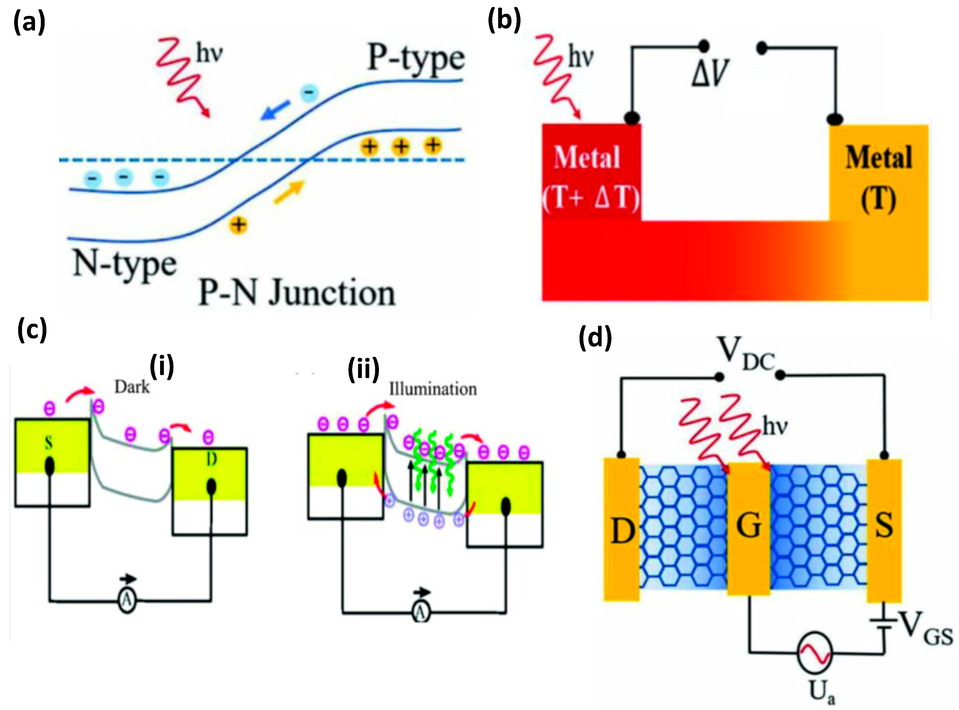
Figure 2.
(a) SEM tilted-view micrograph of Waveguide-integrated graphene mid-infrared photodetector. Inset: Schematic diagram of the device (b) Zero-bias photocurrent recorded as a function of input optical power from the waveguide at 2,185 nm wavelength (c) Responsivity of the detector device to 2,185 nm waveguide input (d) Mid-infrared broadband spectral dependences of the detector’s responsivity (at 1.5 V bias) and calculated optical absorption in the graphene layer. (e,f) On-chip graphene photodetector (e) Front view (f) top view (g) Current responsivity () as a function of wavelength () (h) Minimum detectable concentration () as a function of the source power ()[3,27]
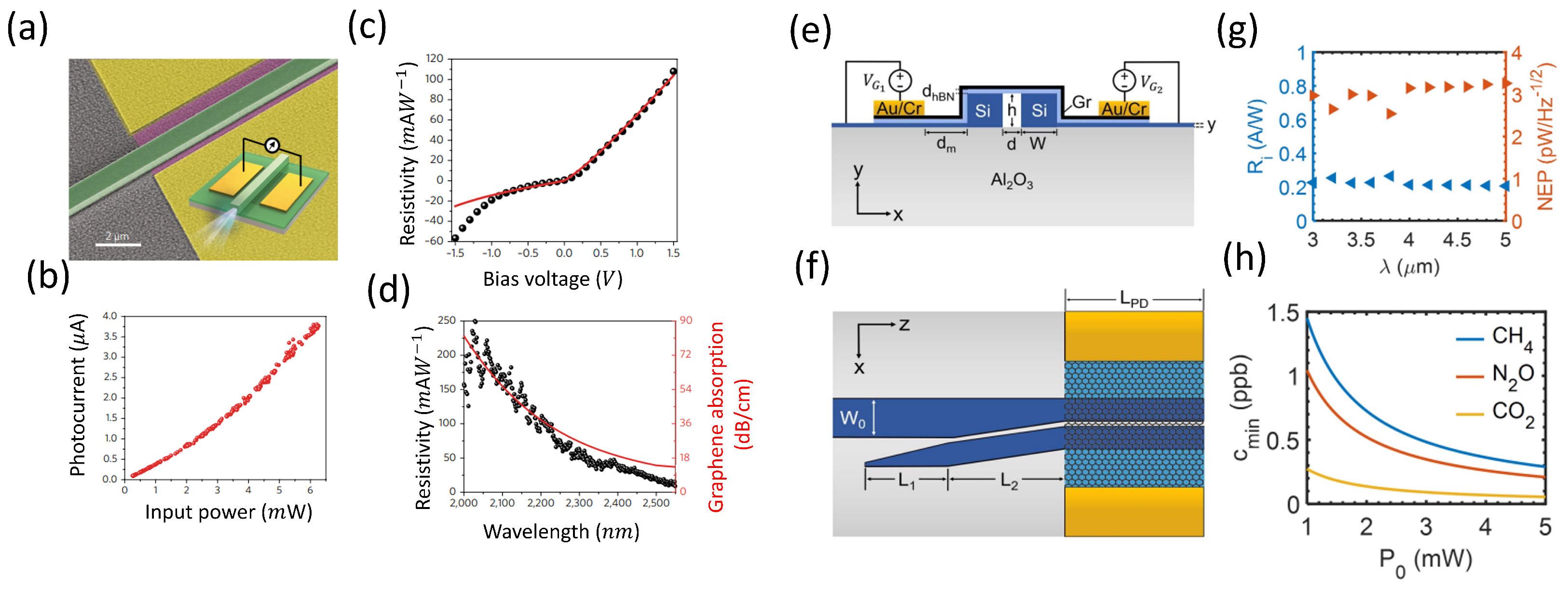
Figure 3.
TMDC photodetectors. (a) Schematic of a MoS2-based photodetector integrated into a photonic circuit, where monolayer MoS2 is directly exfoliated onto the waveguide. (b) Illustration of light coupling achieved by focusing a 647 nm continuous-wave (CW) laser onto the diffraction grating. The light propagates through the Si3N4 waveguide and generates electron–hole pairs in MoS2, leading to photocurrent generation in the biased monolayer. (c) Influence of the MoS2 monolayer and metal contacts on waveguide light propagation. Experimental data compare lateral and vertical absorption as a function of flake length. [36] (d) Schematic showing gate and source–drain bias modulation of the photodetection performance in a vertically stacked 2H-MoS2/1T@2H-MoS2 device. (e) 3D view of photoresponsivity mapping of this device under varying gate and source–drain biases, measured at an illumination power density of 2.35 mW/cm2. [37] (f) Schematic of a MoSe2–WS2 heterostructure photodetector transferred onto a silicon nitride waveguide. Electric field enhancement at the MoSe2/waveguide interface boosts device sensitivity. (g) Frequency response of the photodetector with modulation frequency of incident light is swept, revealing a dB cutoff at ∼20 MHz. The solid line fits an RC low-pass filter model. [38] (h) Schematic of a hyperbolic metamaterial (HMM) nanocavity integrated with a 2D TMDC layer. (i,j) Photocurrent as a function of incident power at resonance (1200 nm) and off-resonance (1064 nm), respectively. A ∼7.5-fold enhancement is observed at ∼0.3 mW for on-resonance excitation, while the off-resonance case shows ∼2.5-fold enhancement at similar power levels. [39]
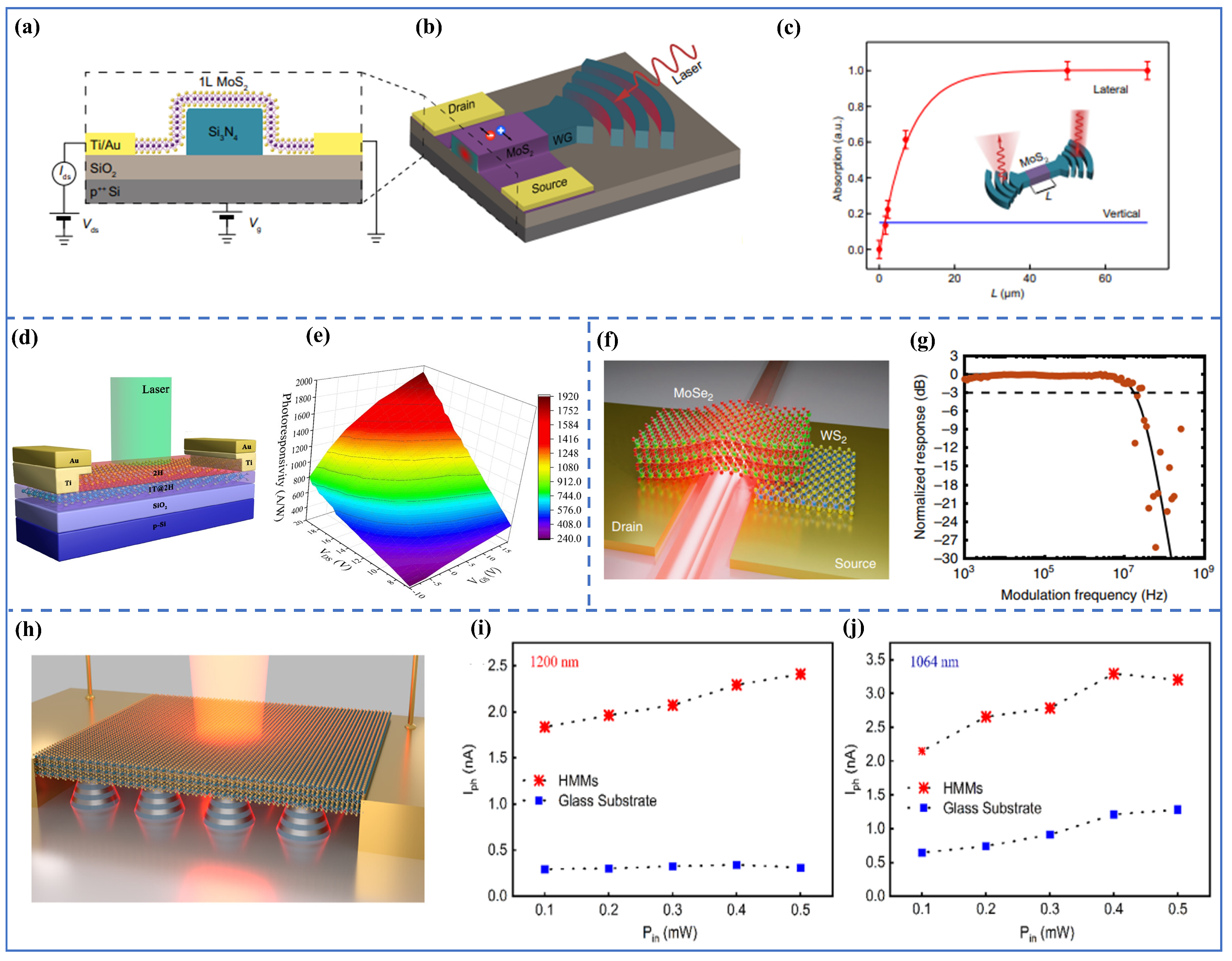
Figure 4.
Different type of BP devices’ architecture. (a) Schematic of the waveguide-integrated van der Waals PN heterojunction photodetector composed of stacking p-doped BP and n-doped MoTe2, which are evanescently coupled with the guiding mode of the silicon nitride waveguide [65]. (b) Top: Band profiles of BP and MoTe2 layers in the non-equilibrium state. Bottom: Band alignment of BP/MoTe2 PN heterojunction in the thermal equilibrium state [65]. (c) Structure of the tunable BP mid-IR photodetector based on a dualgate transistor configuration [66].
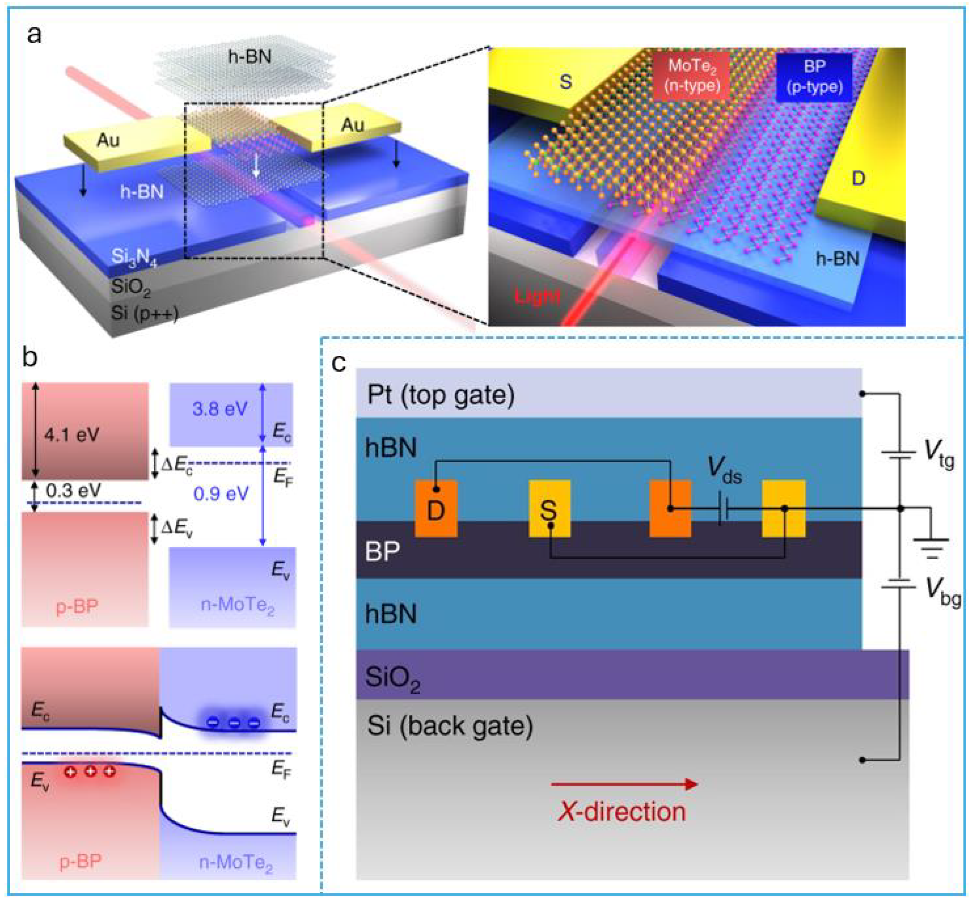
Figure 5.
The schematic diagram (a) and the cross-section view (b) of the as-prepared Ti3C2/Al2O3/Ge vdW Schottky junction. (c) The cross-section SEM image of the vdW Schottky junction. (d) The linear and semi-logarithmic current-voltage curves of the vdW Schottky junction. (e) The curve of dV/dI versus 1/I of the vdW Schottky junction, the inset shows the model of equivalent circuit which consists of an ideal diode and a resistor [72]. (f) and (i) The time-dependent photo-response in self-powered mode according to different light intensities at 980 and 1550 nm, respectively. (g) and (j) The / ratios and photocurrents based on the varying intensities of the incident light at 980 and 1550 nm, respectively. (h) and (k) The calculated values of R and D* according to the varying light intensities at 980 nm and 1550 nm, respectively [72].
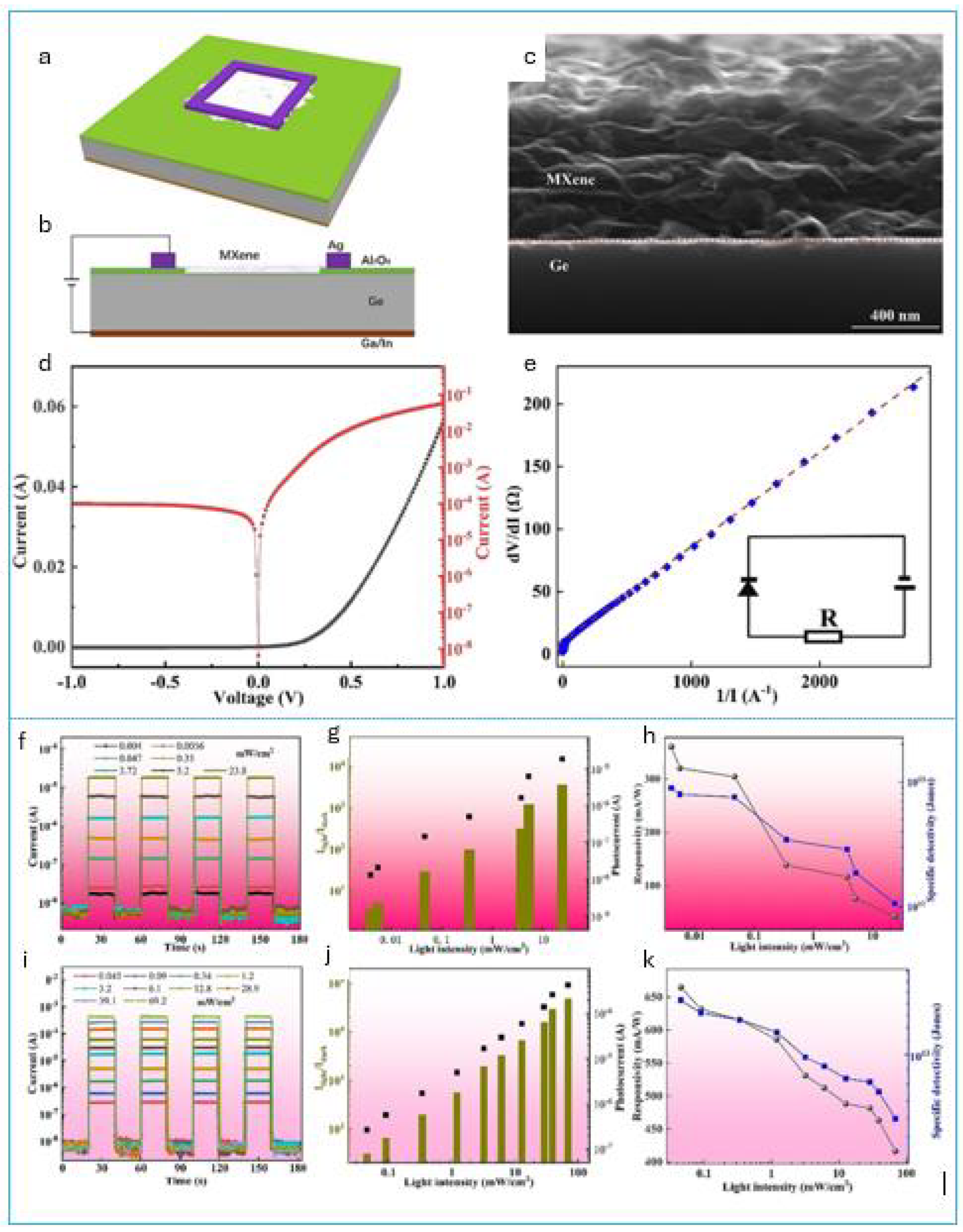
Figure 6.
(a) The schematic hetero-structure of the photodetector fabricated using organic and carbide and (b) The photocurrent results of the photodetector when Using M2 organic material (M2 = 3,6-dibromo-9-(2-ethylhexyl)-9H-carbazole. [94].
Figure 6.
(a) The schematic hetero-structure of the photodetector fabricated using organic and carbide and (b) The photocurrent results of the photodetector when Using M2 organic material (M2 = 3,6-dibromo-9-(2-ethylhexyl)-9H-carbazole. [94].
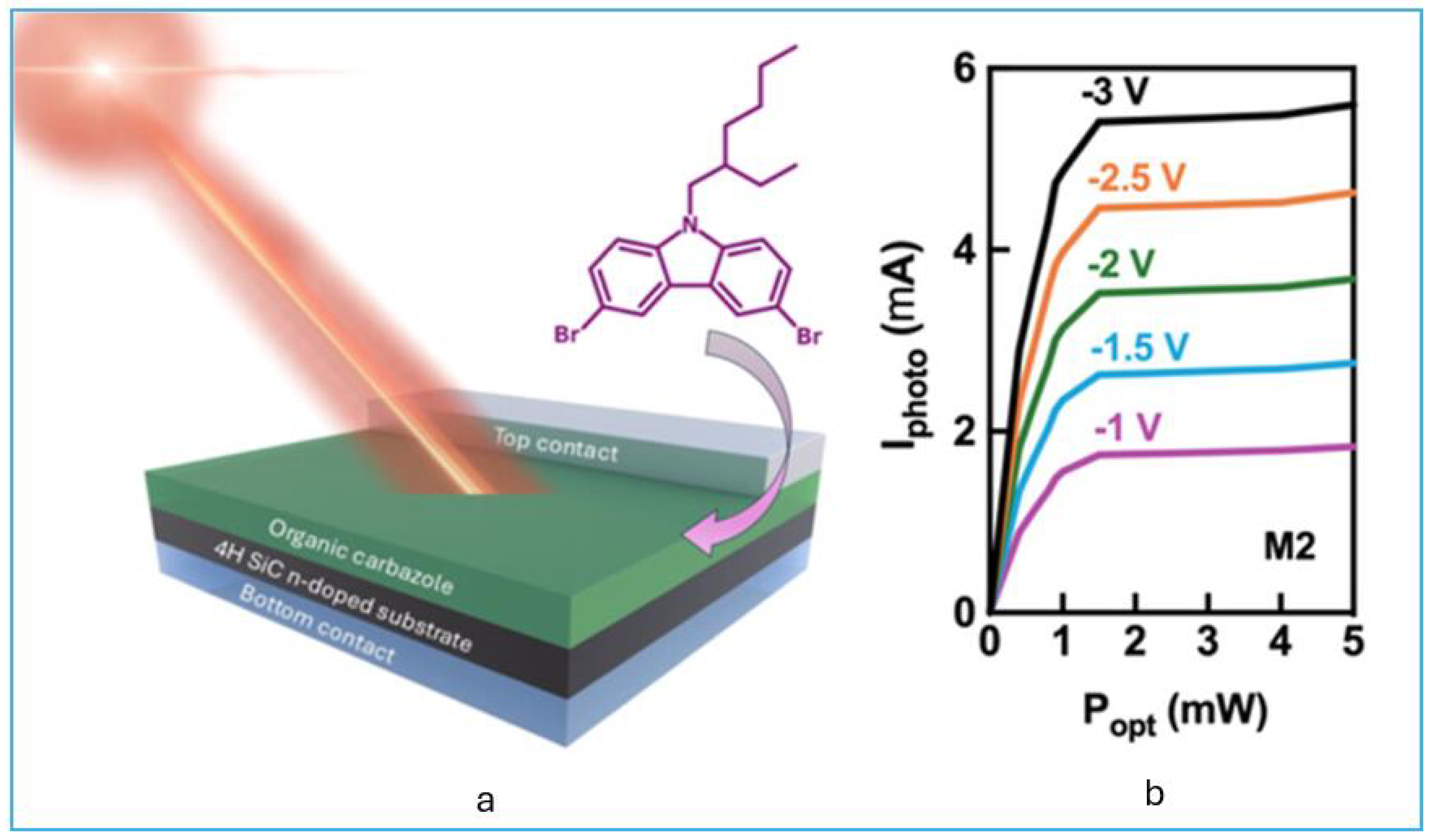
Figure 7.
a) Schematic diagram of photodetection measurement used in this work; (b) I-V characteristic curves of the device with and without 850 nm light illumination under various light intensities; light power intensity-dependent (e) photo-switching behavior, (f) photocurrent, (g) responsivity and specific detectivity of the photodetector at 850 nm [107]. Note: (b)-(d) were conducted at room temperature with a bias voltage of 1V.
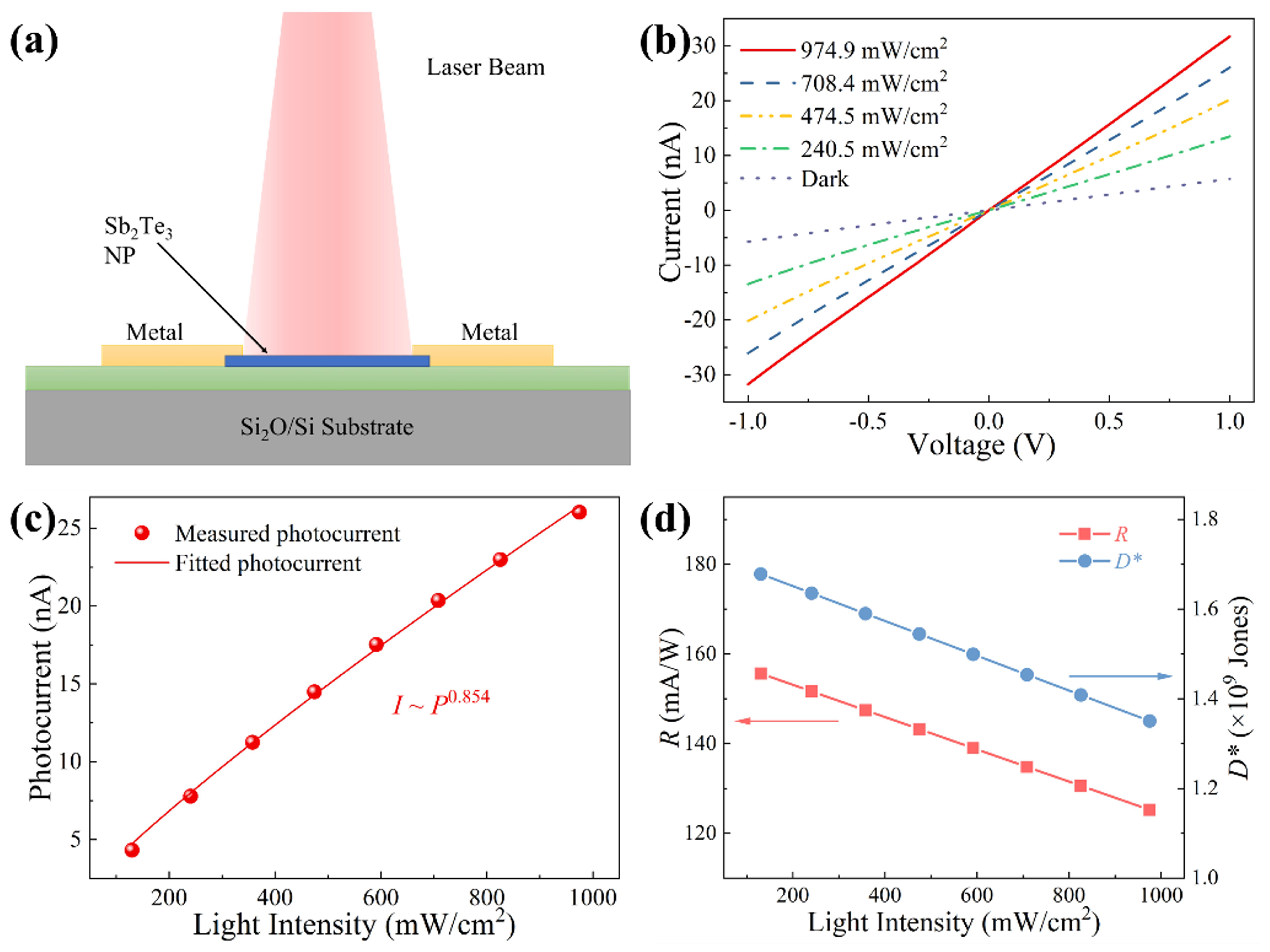
Table 1.
Performance Metrics of Selected 2D-Based Photodetectors
| Material | Spectral Range | Responsivity (A/W) | Detectivity (Jones) | Response Time (ms) | Reference |
|---|---|---|---|---|---|
| Graphene on SOS slot waveguide | MWIR (3 – 5 m) | − | − | [3] | |
| Graphene with ChG waveguide | 2.0 – 2.55 m | − | [27] | ||
| MoS2 | Visible (660 nm) | 880 | 50 | [34] | |
| Te2-regulated black AsP | 2– 8 m | 0.1 – 10 | – | – | [50] |
| BP and Reduced GO | 532 nm – 2200 nm | 12 | 2.4 | – | [53] |
| BP with asymmetric AU | 405 – 1064 nm | 34 | 2.47 | – | [54] |
| BP with asymmetric AU | 2200 nm | 20 | 1.94 | – | [54] |
| BP and MoS2 | 3 – 5 m | – | – | [57] | |
| BP in nanowire | – | 802.42 | – | 6.36 | [58] |
| Monolayer BP-Bi | – | 133 | – | – | [59] |
| MoS2/WO3−x-MoS2 | visible–NIR | [119] | |||
| InSe/WSe2 vdW | 532–1100 nm | [120] | |||
| WS2/ZnO-QD | UV–visible | [121] | |||
| MoSe2/AIGS-QDs | Visible–NIR | − | [122] | ||
| MoTe2/Ta2NiSe5 dual HJ | 400–1550 nm | [123] | |||
| Bi2Te3 nanoplates | 850 nm | − | [101] | ||
| Bi2Se3 nanobelts | 735 nm | [102] | |||
| Bi2O2Se nanoplates | 400 nm | 523 | − | [103] | |
| Sb2Te3 nanoplates | 400–980 nm (max at 850 nm) | [107] | |||
| SnSe nanoplates | 400 nm | − | − | [110] | |
| SnTe nanoplates | 980 nm | − | − | [113] |
Disclaimer/Publisher’s Note: The statements, opinions and data contained in all publications are solely those of the individual author(s) and contributor(s) and not of MDPI and/or the editor(s). MDPI and/or the editor(s) disclaim responsibility for any injury to people or property resulting from any ideas, methods, instructions or products referred to in the content. |
© 2025 by the authors. Licensee MDPI, Basel, Switzerland. This article is an open access article distributed under the terms and conditions of the Creative Commons Attribution (CC BY) license (http://creativecommons.org/licenses/by/4.0/).
Copyright: This open access article is published under a Creative Commons CC BY 4.0 license, which permit the free download, distribution, and reuse, provided that the author and preprint are cited in any reuse.


