Submitted:
27 May 2025
Posted:
28 May 2025
You are already at the latest version
Abstract
To address the need for high performance and low power in edge AI scenarios, this paper proposes a domestically developed smart chip acceleration architecture. It features heterogeneous computing units, a configurable on-chip interconnect, and multi-level energy optimization, enabling balanced computational density and power control with broad algorithm compatibility. The design integrates core modeling, dynamic scheduling, clock gating, DVFS, and data flow reconfiguration to enhance energy efficiency. Experimental results demonstrate superior throughput and power control over comparable chips in typical AI tasks, highlighting strong application potential.
Keywords:
smart chips
; heterogeneous computing
; on-chip networks
; dynamic scheduling
; low-power optimization
1. Introduction
Given diverse model structures and dynamic workloads, building high-performance, low-power intelligent chips is essential for advancing domestic AI hardware[1]. While some international chips excel in reasoning tasks, their specialization, high power usage, and ecosystem constraints limit broader application. To overcome these challenges, this paper proposes a domestic AI chip acceleration architecture, emphasizing heterogeneous computing design, optimized on-chip interconnects, and energy-aware scheduling to achieve near-optimal energy efficiency with high throughput.
2. Heterogeneous Computing Acceleration Unit Design for AI Loads
2.1. Heterogeneous Computing Unit Architecture
As AI integrates into edge computing and industrial control, traditional processors can no longer meet the demands of AI tasks for performance, energy efficiency, and real-time response [2]. Addressing diverse models and dynamic workloads requires high-performance, low-power intelligent chips. Existing international solutions face limitations in power and adaptability. This paper proposes a domestic AI chip architecture with heterogeneous computing, optimized interconnects, and energy-aware scheduling to balance efficiency and throughput.
Figure 1.
Heterogeneous computing unit architecture.
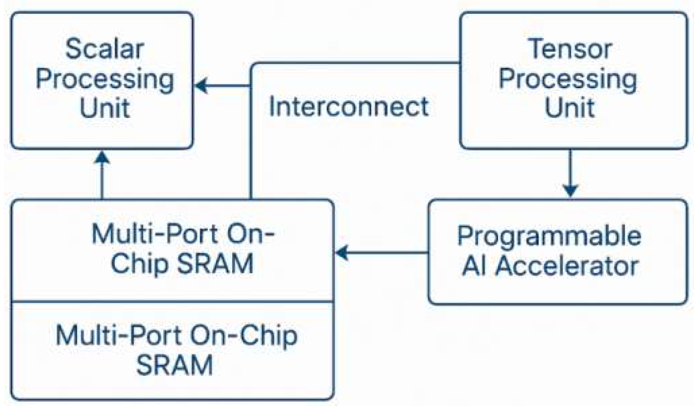
- On-chip network interconnection technology
A configurable mesh-based interconnect is proposed, combining virtual channels and adaptive routing to ensure bandwidth isolation and low communication delay under heavy loads[3]. QoS-aware packet scheduling prioritizes critical operations, while Dynamic Link Width (DLW) and data compression at the physical layer reduce power and congestion [4]. The performance model is constructed based on the node traffic density function and channel bandwidth , and the network delay D can be expressed as:
where is the link length, is the average hop count, and is the link utilization.
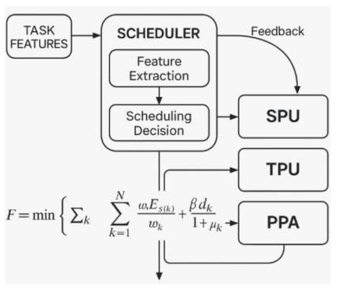
2.2. Dynamic Scheduling of Computing Resources
In order to adapt to the load fluctuation and resource usage imbalance problem during the operation of diverse AI models, this paper constructs a scheduling framework based on task graph topology analysis, combined with Reinforcement Learning Scheduling (RLS) to dynamically match different operators to the optimal computing units. The scheduler monitors the computational density, data dependency depth dk and resource utilization in real time, and optimizes based on the scheduling performance objective function F. The scheduling framework is based on the topology analysis of the task graph:
where wk is the computation amount of the kth task Cs(k) is the computation power of its assigned unit, Es(k) indicates its unit energy consumption; α and β are the regulation coefficients, which optimize the performance and energy consumption.
Figure 2.
Schematic diagram of dynamic scheduling mechanism of computing resources.
3. Low-Power Smart Chip Performance Optimization Methods
3.1. Dynamic Voltage Regulation
This mechanism monitors key parameters such as instruction-level parallelism (ILP), cache hit rate (CHR) and logic unit switching rate (TAR) to predict the current load characteristics, and then adaptively adjusts the operating voltage V of each computational unit and the main frequency f [5]. Under the premise of meeting the performance requirements, the mechanism achieves the optimal global energy efficiency by optimizing the energy-delay product (EDP):
where Ci is the capacitive load of the ith cell, Vi and fi are its current voltage and frequency, ti is the task execution time, ΔPi indicates the offset from the standard power consumption, and κ is the stability penalty factor.
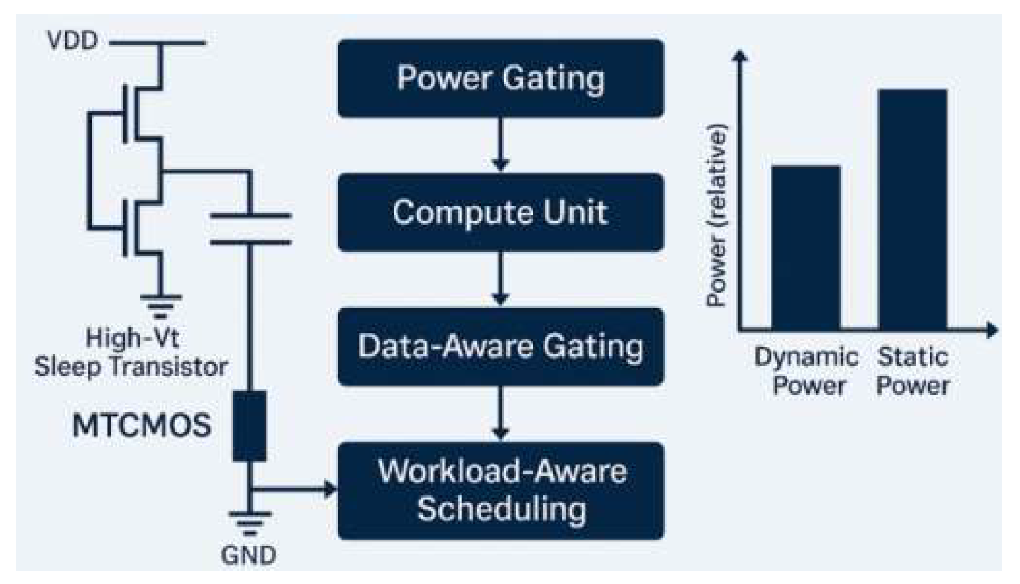
3.2. Reduction of Computing Unit Power Consumption
This paper proposes a multi-level power reduction strategy combining logic-level low-power design (e.g., MTCMOS), micro-architecture-level power gating, and algorithm-level sparse-aware scheduling [6]. Static power is reduced by using high-threshold transistors to power down idle units and enter sleep mode during low-load phases. For dynamic power, a data-aware gating mechanism selectively disables low-activity signal paths. The total power consumption is modeled by integrating contributions from multiple power sources.:
where αi is the activity factor of the ith computational unit, Ci is the capacitance, Ileaki denotes its leakage current under the condition of temperature Tand voltage Vi, 1idle(i) is the idle indicator function, and γi is the turn-off cost factor.
Figure 3.
Schematic diagram of the multi-level power reduction mechanism.
3.3. Local Clock Gating and Data Flow Optimization
Large-scale clock trees in smart chips generate significant dynamic power, especially under partial or low-load conditions. To enhance energy efficiency, this paper employs Fine-Grained Clock Gating (FGCG) and Data Flow Reallocation (DFR) [7]. FGCG selectively activates clocks in MAC units, control logic, and caches only during active compute cycles, guided by instruction scheduling and workload awareness. DFR dynamically reallocates data paths based on flow intensity, optimizing bandwidth use and cache performance. Simulation results on Transformer inference tasks confirm the effectiveness of these techniques:

Table 1.
Impact of Clock Gating and Data Flow Optimization on Performance and Power Consumption Table.
Table 1.
Impact of Clock Gating and Data Flow Optimization on Performance and Power Consumption Table.
| optimization strategy | Chip Power Consumption Reduction (%) | Average delay reduction (%) | On-chip cache hit rate improvement (%) | Decrease in the number of clock switches (%) |
|---|---|---|---|---|
| no optimization | 0.0 | 0.0 | 0.0 | 0.0 |
| FGCG alone | 17.3 | 3.5 | 1.2 | 36.8 |
| DFR alone | 8.9 | 9.4 | 12.6 | 4.1 |
| FGCG + DFR Joint Optimization | 24.7 | 11.2 | 13.9 | 39.3 |
4. Validation and Experimental Analysis
4.1. Experimental Platform and Test Program
To evaluate the low-power performance of the proposed domestic smart chip, an experimental platform integrating hardware simulation, system verification, and algorithm testing is built. Based on a 28nm CMOS prototype with heterogeneous units, configurable interconnects, clock gating, and multi-domain DVFS, the system runs on a Xilinx VCU128 board with precision power monitoring.Tests include CNN inference (ResNet-50, MobileNetV2), NLP (BERT-base), and unstructured tasks (e.g., sparse matrix ops), measuring throughput (TOPS), energy efficiency (TOPS/W), latency, and power. Cold-start averaging and calibration ensure accuracy.
4.2. Performance Test Results
As described in Section 4.1, the chip's core performance is evaluated using three typical AI tasks: image recognition (ResNet-50), semantic understanding (BERT-base), and sparse computation (Sparse GEMM) [10]. Metrics include throughput (TOPS), energy efficiency (TOPS/W), latency, and on-chip power at peak load and 1.0 GHz, benchmarked against mainstream AI chips.Results show that the proposed heterogeneous architecture, with dynamic voltage control, optimized interconnects, and resource scheduling, outperforms peers in both speed and efficiency. In particular, for BERT, the programmable accelerator’s optimization of Transformer operations enables performance exceeding 21 TOPS, surpassing comparable domestic chips.
Table 2.
Performance test results of the chip under different AI tasks.
| Model Type | test task | Chip Throughput Rate (TOPS) | Energy Efficiency Ratio (TOPS/W) | Average delay (ms) | Chip Power Consumption (W) |
|---|---|---|---|---|---|
| image recognition | ResNet-50 | 18.4 | 9.7 | 3.21 | 1.89 |
| language understanding | BERT-base | 21.3 | 10.2 | 4.85 | 2.09 |
| sparse computing | Sparse GEMM | 16.2 | 11.5 | 2.74 | 1.41 |
4.3. Comparative Analysis with International Similar Chips
To assess the international competitiveness of the proposed chip, this paper compares it with three mainstream AI accelerators: NVIDIA Jetson Xavier NX (GPU), Google Edge TPU (ASIC), and Huawei Rise 310 (domestic AI chip). Under a unified test setup with identical batch sizes and FP16 precision, ResNet-50 and BERT-base models are used to evaluate peak throughput, energy efficiency (TOPS/W), and average latency.Results show that the chip matches Jetson Xavier NX in throughput and exceeds it in energy efficiency, particularly in Transformer tasks due to optimized operator scheduling.
Table 3.
Comparison of the performance of the national chips with their international counterparts.
| chip platform | test model | Throughput Rate (TOPS) | Energy Efficiency Ratio (TOPS/W) | Average delay (ms) | Remarks |
|---|---|---|---|---|---|
| This design chip | BERT-base | 21.3 | 10.2 | 4.85 | Supports heterogeneous scheduling with DVFS |
| Jetson Xavier NX | BERT-base | 22.5 | 6.9 | 5.37 | GPU architecture with high power consumption |
| Google Edge TPU | ResNet-50 | 14.8 | 8.2 | 3.95 | Fixed structure with limited sparse support |
| Huawei Rise 310 | BERT-base | 19.6 | 9.1 | 5.02 | Universal NPU Platform |
5. Conclusions
This paper presents a low-power acceleration architecture for domestic AI chips, featuring heterogeneous computing, optimized on-chip networks, and dynamic resource scheduling. Structurally, the integration of scalar processors, tensor units, and programmable AI modules enables efficient task-specific computation. Energy efficiency is enhanced through multi-domain DVFS, voltage gating, and local clock shutdown, reducing both static and dynamic power. An adaptive scheduling model based on task topology and real-time feedback improves efficiency under complex loads.
Experiments show strong throughput and energy efficiency on models like ResNet and BERT, with superior power control and scheduling flexibility compared to international counterparts, and excellent edge deployment adaptability. Future work will explore multi-core collaboration, inter-chip communication, and domain-specific acceleration to support large-scale deployment of high-efficiency domestic AI chips.
References
- Zhou D. Intelligent LED lighting control system design and realization. Journal of Physics: Conference Series 2024, 2810, 012005–012005. [Google Scholar]
- Li Z,Xu H,Lyu R. Effectiveness analysis of the data-driven strategy of AI chips supply chain considering blockchain traceability with capacity constraints. Computers & Industrial Engineering 2024, 189, 109947. [Google Scholar] [CrossRef]
- Kim H,Woda C,Discher M. OSL at elevated temperature of smart chip cards for retrospective dosimetry. Radiation Physics and Chemistry 2024, 217, 111520. [Google Scholar] [CrossRef]
- Le Y,Zhixuan W,Tianyu J, et al. Research progress on low-power artificial intelligence of things (AIoT) chip design. Science China Information Sciences 2023, 66, 36–38. [Google Scholar]
- Guodong W,Tingyu C,Lanlan G, et al. Highly responsive gas sensor based the Au-ZnO films processed by combining magnetron sputtering and Ar plasma treatment. Physica Scripta 2023, 98, 502–505. [Google Scholar]
- Min Z,Qi L,Shen Y, et al. Co-proliferation of antimicrobial resistance genes in tilapia farming ponds associated with use of antimicrobials. The Science of the total environment 2023, 887, 164046. [Google Scholar] [CrossRef] [PubMed]
- Lulu C,Jinlu S,Yanzhi S, et al. Intelligent Chip-Controlled Smart Oxygen Electrodes for Constructing Rechargeable Zinc-Air Batteries with Excellent Energy Efficiency and Durability. ACS applied materials & interfaces 2023, 15, 1170–1175. [Google Scholar]
- Vogt W. Ag autonomy firm turns to smarter chip. Farm Industry News 2022, 17, 22–23. [Google Scholar]
- Momose H,Kaneko T,Asai T. Systems and circuits for AI chips and their trends. Japanese Journal of Applied Physics 2020, 59, 050502. [Google Scholar] [CrossRef]
- Hui X. Low-power approximate multipliers for artificial intelligence chips. Ocean University of China (China) 2023, 28, 86–88. [Google Scholar]
Disclaimer/Publisher’s Note: The statements, opinions and data contained in all publications are solely those of the individual author(s) and contributor(s) and not of MDPI and/or the editor(s). MDPI and/or the editor(s) disclaim responsibility for any injury to people or property resulting from any ideas, methods, instructions or products referred to in the content. |
© 2025 by the authors. Licensee MDPI, Basel, Switzerland. This article is an open access article distributed under the terms and conditions of the Creative Commons Attribution (CC BY) license (http://creativecommons.org/licenses/by/4.0/).
Copyright: This open access article is published under a Creative Commons CC BY 4.0 license, which permit the free download, distribution, and reuse, provided that the author and preprint are cited in any reuse.


