
Submitted:
17 May 2025
Posted:
20 May 2025
You are already at the latest version
Abstract
This study investigates the structural, luminescent, and photoconversion properties of composite converters based on epitaxial structures containing single-crystalline films of Ce³⁺-doped Ca₂₋ₓY₁₊ₓMg₁₊ₓSc₁₋ₓSi₃O₁₂:Ce (x=0–0.25) (CYMSSG:Ce) garnet, and Y₃Al₅O₁₂ (YAG) or YAG:Ce substrates, grown using the Liquid Phase Epitaxial (LPE) method. The research focuses on a detailed analysis of the properties of film-crystal composite converters to achieve a deeper understanding of their photoconversion performance, providing an innovative approach to designing a new type of film/ substrate converters for white LEDs. This was accomplished by systematically varying the Y/Sc/Mg cation content in the film and adjusting the film thickness within the range of 19–67 µm for CYMSSG:Ce/YAG structures and 10–22 µm for CYMSSG:Ce/YAG:Ce structures. A significant emphasis of this research was placed on mapping the performance of these converters using a color coordinate diagram, a key tool for visualizing the relationship between film composition, thickness, and photoconversion efficiency. The resulting data revealed clear and distinct trends, offering valuable insights into the tunability of the luminescent properties of white LEDs through precise control of content and film thickness.
Keywords:
mixed garnets
; Ca-Mg-Si based garnets
; Ce3+ dopant
; liquid phase epitaxy
; single crystalline films
; substrates
; luminescence
; phosphor-converters
1. Introduction
In recent years, the demand for high-efficiency, energy-saving light sources has significantly increased, driven by advancements in lighting and display technology. White light-emitting diodes (WLEDs) have emerged as the dominant choice due to their superior energy efficiency, long lifespan, and environmental benefits, including reduced carbon emissions and lower energy consumption compared to traditional incandescent and fluorescent bulbs [1]. Additionally, WLEDs have found applications beyond general lighting, such as in automotive headlights, backlighting for displays, and even in medical devices, further fuelling the need for continuous improvements in their performance and efficiency [2,3].
A critical factor in the overall performance of WLEDs is the phosphor conversion layer, which plays a central role in colour rendering and light quality. In most WLED configurations, a blue LED chip is combined with a phosphor material that converts a portion of the blue light into yellow, red, or green light, resulting in a balanced white emission. The efficiency of this conversion process directly impacts the brightness, colour rendering index (CRI), and colour correlated temperature (CCT) of the emitted light, all of which are crucial parameters for various applications [4,5,6].
The choice of phosphor material is therefore essential to the performance of the device. Among the various phosphor materials available, garnet-based materials doped with rare-earth ions, especially Ce³⁺, have proven to be among the most effective due to their broad excitation and emission spectra, high quantum efficiency, excellent luminescent properties, and thermal stability under high-power operation [7,8,9,10,11,12]. In particular, the Ce³⁺-doped Y₃Al₅O₁₂ (YAG) phosphor is widely used in the industry for producing high efficiency and good colour quality of white light. It is compatible with blue LEDs and offers advantages such as strong absorption in the blue region, stable emission characteristics, and high thermal stability, which is crucial for maintaining performance over long operating hours [13,14,15,16].
Silicate garnets such as (Ca,Y)₃(Mg,Sc)₂Si₃O₁₂ (CYMSSG) doped with Ce³⁺ ions have shown great potential as phosphor materials due to their broad emission spectra and strong absorption in the blue region, which aligns well with the emission of blue LEDs [8,9,14,15]. However, despite the promising properties of these materials, research on the use of CYMSSG:Ce crystals [19] or single crystalline films (SCF) [16,17,18] as phosphor converters is limited, with even less focus on their performance in composite film-crystal structures [19]. This gap hinders a complete understanding of how these materials behave under real LED excitation conditions and how variations in film structure, particularly thickness, influence their photoconversion efficiency.
The present study addresses this gap by investigating the structural, luminescent, and photoconversion properties of epitaxial converters based on Ce³⁺-doped CYMSSG-based SCFs with varying cation content. These films were crystallized using the Liquid Phase Epitaxy (LPE) method onto YAG and YAG:Ce single-crystal (SCF) substrates, allowing precise control over the growth process and material properties [16,17,18]. By systematically varying the film's cation composition and thickness—ranging from 19–67 µm for Ce³⁺-doped CYMSSG films on YAG crystals (Series A) and 10–22 µm for those on YAG:Ce crystals (Series B)—we thoroughly examined how these parameters influence photoconversion efficiency.
This systematic approach enabled the observation and mapping of distinct trend lines in a chromaticity or colour coordinate diagram, clearly illustrating the relationship between film content, thickness, and photoconversion performance. Variations in content and thickness affected key parameters, such as emission spectra and colour rendering, which are critical for optimizing the overall luminescence and efficiency of the converter. These trend lines provide valuable insights into the optimal content and film thickness required for enhanced photoconversion, highlighting the importance of precise control over SCF parameters to achieve the desired optical characteristics in phosphor converters for WLED applications.
2. SCF Growth and Experimental Techniques
Two distinct sets of thin films with nominal compositions of Ce³⁺-doped Ca₂YMgScSi₃O₁₂ and Ca₁.₇₅Y₁.₂₅Mg₁.₂₅Sc₀.₇₅Si₃O₁₂ (Series A and B, respectively), with thicknesses ranging from 10 µm to 67 µm, were fabricated using the LPE method. The films were crystallized within a temperature range of 975–990 °C from a supercooled melt solution composed of a PbO:B₂O₃ flux with a mole ratio of 12:1. The CYMSSG SCFs were grown on undoped YAG substrates for Series A and on Ce³⁺-doped YAG substrates for Series B, with orientations close to the (111) crystallographic plane. The YAG and YAG:Ce substrates used in these experiments had a thickness of 0.5 mm. The nominal Ce concentration in the CYMSSG:Ce SCFs and YAG:Ce substrates was approximately 0.05-0.15 at. % and 0.05-0.06 at.%, respectively (Table 1). Further details about the growth process for Ca-Si-based films and the specific mole ratios used for LPE growth can be found in references [16,17].
The thickness of the single-crystalline film (SCF), denoted as h (in μm), was determined using a weighing method. This approach involved measuring the substrate’s mass before and after the SCF growth cycle with high-precision scales. Film thickness was then calculated using the formula: h = (m - ms) / (2 × S × ρ), where m is the mass of the substrate with the grown SCF (in grams), ms is the mass of the substrate (in grams), S is the substrate area (in cm²), and ρ is the film density (in g/cm³).
The compositions of single crystals and films were analysed using a JEOL JSM-820 electron microscope (JEOL Ltd., Akishima, Japan) equipped with an IXRF 500i LN₂ Eumex EDX detector (IXRF, Inc., Austin, TX, USA). This advanced tool provided rapid assessments and ensured precise detection of elemental variations with an accuracy of ±1%. The analysis revealed considerable deviations in the concentrations of Ca, Mg, Sc, and Si cations compared to the nominal (in-melt) formulas (Ca,Y)₃(Mg,Sc)₂Si₃O₁₂ and Ca₁.₇₅Y₁.₂₅Mg₁.₂₅Sc₀.₇₅Si₃O₁₂:Ce. Meanwhile, these deviations were consistently less than ± 0.2 formula units, as shown in Table 1. Such findings underscore the importance of precise compositional control in material synthesis. To maintain clarity and alignment with experimental results, the study consistently refers to the nominal composition of the SCFs. This approach ensures standardized comparison while accounting for slight variations observed during the evaluation process.
The structural quality of Ca₂₋ₓY₁₊ₓMg₁₊ₓSc₁₋ₓSi₃O₁₂:Ce (x = 0–0.25) films grown on YAG substrates was investigated using X-ray diffraction (XRD) with a DRON 4 spectrometer equipped with a CuKα X-ray source. For this analysis, Samples B1 and B4 with x=0 and x=1.25 were chosen, featuring a 0.25 Ce³⁺ concentration of 0.01 and 0.15 at.% and a thickness of 19 µm, and 67 µm, respectively, as illustrated in Figure 1 and Table 1. This sample was selected for its suitability for detailed structural evaluation.
Typically, the single crystallinity of CYMSSG films grown on YAG substrates is confirmed using thinner samples, generally with thicknesses of less than 50-70 µm. This preference is driven by the inherent limitations associated with X-ray diffraction in thicker samples. Specifically, the garnet matrix of CYMSSG films exhibits medium X-ray absorption, which changes the relative intensity of diffraction reflections from the YAG substrate. This effect becomes more pronounced as film thickness increases, complicating accurate structural characterization in thicker samples (Figure 1).
Therefore, thinner samples are prioritized for initial analysis to reliably confirm single crystallinity. Once verified, the growth process continues to produce thicker films (exceeding 100 µm) for further experimental studies. This sequential approach ensures that the structural integrity and quality of the CYMSSG films are thoroughly assessed before the fabrication of thicker film samples. By addressing the technical constraints of XRD analysis, this method provides a robust framework for characterizing the structural properties of CYMSSG films on YAG substrates, paving the way for their application in advanced optical and photonic systems.
The lattice misfit between the CYMSSG SCFs and the YAG substrate was calculated using the XRD pattern corresponding to the (12 0 0) crystallographic plane of the sample (Figure 1). The standard formula for lattice misfit, expressed as Δa = ((aSCF - asub) / asub) × 100%, was used, where aSCF is the lattice parameter of the film, and asub is the lattice parameter of the YAG substrate. Analysis revealed a lattice mismatch of 2.51–2.57%, indicating a very large mismatch between the SCF and the substrate. Meanwhile, even this degree of mismatch was found to be consistent with high-quality epitaxial growth, where strain and stress at the interface are not yet critical, maintaining the crystalline integrity of the film.
This finding is particularly significant as it confirms the successful epitaxial growth of the CYMSSG (x=0-0.25) film on the YAG substrate. The low lattice misfit highlights the compatibility of the SCF with the substrate, a crucial factor for ensuring the film's stability and optical performance. By validating the high crystalline quality of the sample, this analysis establishes a strong foundation for further investigations into the luminescent and photoconversion properties of the developed SCFs in advanced photonic applications.
To comprehensively investigate the properties of the two sets of thin-film samples (Series A and B) and Ce-doped substrates (Series C), an extensive suite of spectroscopic techniques was employed. These techniques included absorption spectroscopy, photoluminescence (PL) emission, and excitation (PLE) spectroscopy, which together provided a detailed evaluation of the luminescent characteristics of the CYMSSG:Ce SCFs. All spectroscopic measurements were conducted under ambient conditions at room temperature (RT), ensuring their relevance to practical applications.
The absorption spectra of the SCFs were recorded using a Jasco V730 spectrophotometer (Tsukuba, Japan), a reliable instrument for capturing the films' absorption characteristics. These data served as a foundation for understanding the optical behaviour of the CYMSSG SCFs. For a detailed examination of photoluminescent properties, an FS-5 spectrometer (Edinburgh Instruments, Livingston, UK) was used. This high-precision instrument enabled the acquisition of both PL and PLE spectra, providing insights into the emission and excitation mechanisms within the SCFs.
To further explore the photoconversion behavior of the samples, photoconversion spectra were recorded using an AvaSpec-ULS 2048-LTEC fiber-optic spectrophotometer, paired with an AvaSphere-50-IRRAD integrating sphere (Avantes, Netherlands). These measurements enabled a comprehensive analysis of the SCFs' photoconversion performance, shedding light on their potential for advanced photonic applications.
3. Absorption and Luminescent Properties
3.1. Absorption Spectra
The absorption spectra of the CYMSSG:Ce SCF/YAG SCFs (Figure 2a) and CYMSSG:Ce SCF/ YAG:Ce (Figure 2b) composite samples as well as the absorption spectra of the YAG:Ce SC substrates (Figure 2c), exhibit distinct features in the 200–500 nm wavelength range, reflecting their optical properties. Notably, broad absorption bands peaked around 341 nm and within the 439–457 nm range, referred to as E2 and E1 bands, respectively, are consistently observed across all analysed structures confirming their successful incorporation into the CYMSSG films. These bands are characteristic for absorption of Ce³⁺ ions in the garnet host, corresponding to the 4f¹(²F₅/₂) → 5d (²E) electronic transitions. Additionally, a spectral feature at 230 nm is attributed to the 4f (²F₅/₂) → 5d₁ (T₂g) transitions of Ce³⁺ ions (E3 band). These identifications align with prior studies, which highlight these transitions as key spectral signatures of Ce³⁺ ions in garnet matrices [1,2].
Another notable feature of SCF samples is an absorption band 300 nm and below, linked to the 1S₀ →3P₁ and 1P₁ electronic transition of Pb²⁺ impurity, likely introduced in the film during LPE their growth from PbO-based flux. The last Pb2+ related band strongly overlapped with E3 band of Ce3+ ions. Despite being associated with trace Pb²⁺ inclusions, this feature provides valuable insights into the real material's composition and the interactions between dopants and Ce3+ ions [3].
In addition to these primary features, low intensive absorption bands in the UV range, peaking at 370 nm, are evident in the YAG:Ce substrates and absorption spectra of CYMSSG:Ce SCF/YAG:Ce sructure. Generally, such UV bands have been attributed to defect center absorption in garnets, grown or annealed in the reducing atmosphere [19], or containing excess of Ca²⁺ and Mg²⁺ ions [8,14,17,18], and correspond to the absorption of F+ center (one-charged anion vacancy).
Overall, the analysis of these absorption spectra confirms the effective doping of the SCFs with Ce³⁺ ions and underscores the impact of trace impurities on their optical behaviour. This detailed evaluation provides a foundation for understanding the luminescent properties of these composite structures and their potential in photonic and optoelectronic applications.
3.2. PL Spectra
The PL and PLE spectra of samples from Series A and B, as well as substrates from Series C, are shown in Figure 3. The PL spectra of all SCF samples (Figure 3a,b) exhibit intense luminescence characterized by broad emission bands in the green-yellow spectral range. These bands are attributed to the 5d₁→4f (²F₅/₂, ²F₇/₂) electronic transitions of Ce³⁺ ions, which are characteristic of the luminescent behaviour of cerium-doped garnets. However, it should be noted that Ce³⁺ emission bands consist of several sub-bands corresponding to non-equivalent Ce³⁺ multicenters. Specifically, Ce³⁺ ions replace the dodecahedral positions of Ca²⁺ and Y³⁺ cations, which have different local surroundings with Mg²⁺ and Sc³⁺ ions in octahedral positions and Si⁴⁺ in tetrahedral positions within the garnet lattice. The observed structure of the PL spectra of CYMSSG:Ce SCFs grown on a YAG substrate clearly indicates the presence of multiple Ce³⁺ emission centers in the CYMSSG host, as described in detail in our previous works [8,16].
The PL spectrum of samples from Series A, which were grown on an undoped YAG substrate, exhibits a broader Ce³⁺ luminescence band with two distinct peaks at 510 nm and 548 nm. The slight blue shift in the PL emission and excitation spectra of sample A1 is caused by its lower cerium concentration, which is three times lower than that of the other samples in this set. This blue shift occurs because the reduced Ce³⁺ concentration limits energy transfer between different Ce³⁺ multicenters, primarily affecting those emitting in the longer-wavelength range.
Conversely, the PL spectra of samples from Series B, grown on a Ce³⁺-doped YAG substrate, display a notably broader emission band with peaks at 536 nm and 573 nm due to the overlap between the PL spectra of the YAG:Ce substrate (Figure 3c) and the CYMSSG:Ce SCFs (Figure 3a). This red shift may also result from variations in the crystal field strength or changes in the covalency of Ce³⁺-ligand bonds within the Ca²⁺-Si⁴⁺-based CYMSSG host compared to the YAG:Ce substrate [8,16]. Specifically, increased covalency in Ce³⁺-ligand bonds within the CYMSSG matrix reduces the energy required for Ce³⁺ electronic transitions, contributing to the observed red shift.
Interactions between Ce³⁺ ions in YAG:Ce substrates and CYMSSG:Ce films may also lead to energy transfer processes that influence the emission spectra of the epitaxial structure. Understanding these wavelength shifts is crucial for tailoring the material's properties and optimizing its emission for specific applications. These findings highlight the critical role of substrate composition in determining the photoluminescence properties of CYMSSG:Ce films. The interactions between SCFs and substrates, particularly those involving cerium doping, significantly impact energy transfer dynamics and luminescent behavior. Such insights are essential for designing and optimizing photoluminescent materials for advanced optical and lighting applications, where precise control over emission characteristics is required.
3.3. PLE Spectra
The PLE spectra of Ce³⁺ ions in YAG:Ce substrates and CYMSSG SCF/YAG and CYMSSG SCF/YAG:Ce structures are presented in Figure 4b,d,f. The 4f (²F₅/₂) → 5d transitions are key characteristics of Ce³⁺ ion excitation and play a fundamental role in its luminescent behaviour. The peak near 456 nm in YAG:Ce substrates is typically associated with the transition from the ground state to the lowest 5d energy level, whereas the 340 nm peak corresponds to a transition to a higher-lying 5d state. These transitions are governed by the symmetry and electronic environment of Ce³⁺ ions within the garnet matrix. The relative intensities and positions of these bands provide insights into the local crystal field and the energy splitting of the 5d states.
Furthermore, the peaks at 340 nm and 456 nm indicate that the YAG:Ce substrate and its composite structure exhibit efficient absorption capabilities at multiple wavelengths, enabling excitation in both the UV and visible regions. This dual-excitation feature enhances the material’s photoluminescent properties, making it suitable for applications in lighting, displays, and optoelectronic devices.
The PLE spectra for Series A (Figure 3b) exhibit prominent maxima at 346 nm and 454 nm, corresponding to the 4f → 5d electronic transitions of Ce³⁺ ions in the CYMSSG host. These peaks are typical of cerium-doped materials and indicate efficient absorption in the UV and blue regions, making them suitable for excitation by respective LEDs.
The PLE spectra of samples from Series B (Figure 3d) represent a superposition of the PLE spectra of the YAG:Ce substrate and CYMSSG:Ce SCF. These spectra feature a peak at 343 nm (E₂) and a broad complex excitation band in the blue region centered at 472 nm (E₁). The latter band is a superposition of at least two distinct peaks located at 433 nm and 476 nm. The presence of multiple peaks within the E₁ band is typically attributed to the excitation of Ce³⁺ multicenters in the CYMSSG:Ce film [8,16].
The excitation peak observed at 375 nm in the PLE spectra of Ce³⁺ luminescence in CYMSSG:Ce SCFs is closely related to intrinsic electronic transitions associated with F⁺ centers in garnets [17,18]. Specifically, this peak corresponds to the ¹A → ¹B transition of the F⁺ center, a well-known defect in many crystalline materials, including oxides. The F⁺ center refers to an oxygen vacancy typically associated with a trapped electron. The presence of this excitation band at 375 nm suggests that F⁺ centers play a role in the optical behaviour of CYMSSG:Ce SCFs, contributing to the material’s overall photonic properties. In particular, the material’s ability to absorb light at this wavelength may influence the efficiency of energy transfer processes and the overall photoluminescent behaviour of Ce³⁺ ions, as interactions between F⁺ centers and Ce³⁺ ions can modify emission characteristics.
5. Photoconversion Properties
Prototypes of phosphor-converted white light-emitting diodes (pc-WLEDs) were developed to assess their performance and to investigate how the content and thickness of SCFs affect the colorimetric properties of SCF and composite converters. These pc-WLEDs were assembled by integrating SCFs and composite converters onto InGaN blue-emitting chips with a peak emission wavelength of 450 nm. These chips operated at a forward-bias voltage of 2.6 V and a drive current of 20 mA.
Figure 4.
Normalized emission spectrum of pc-WLED prototypes fabricated on the base of 450 nm LED chip and CYMSSG:Ce SCF converter grown onto YAG (a) and YAG:Ce (b) substrates in comparison with converters on the base of YAG:Ce crystal-substrates (c).
Figure 4.
Normalized emission spectrum of pc-WLED prototypes fabricated on the base of 450 nm LED chip and CYMSSG:Ce SCF converter grown onto YAG (a) and YAG:Ce (b) substrates in comparison with converters on the base of YAG:Ce crystal-substrates (c).
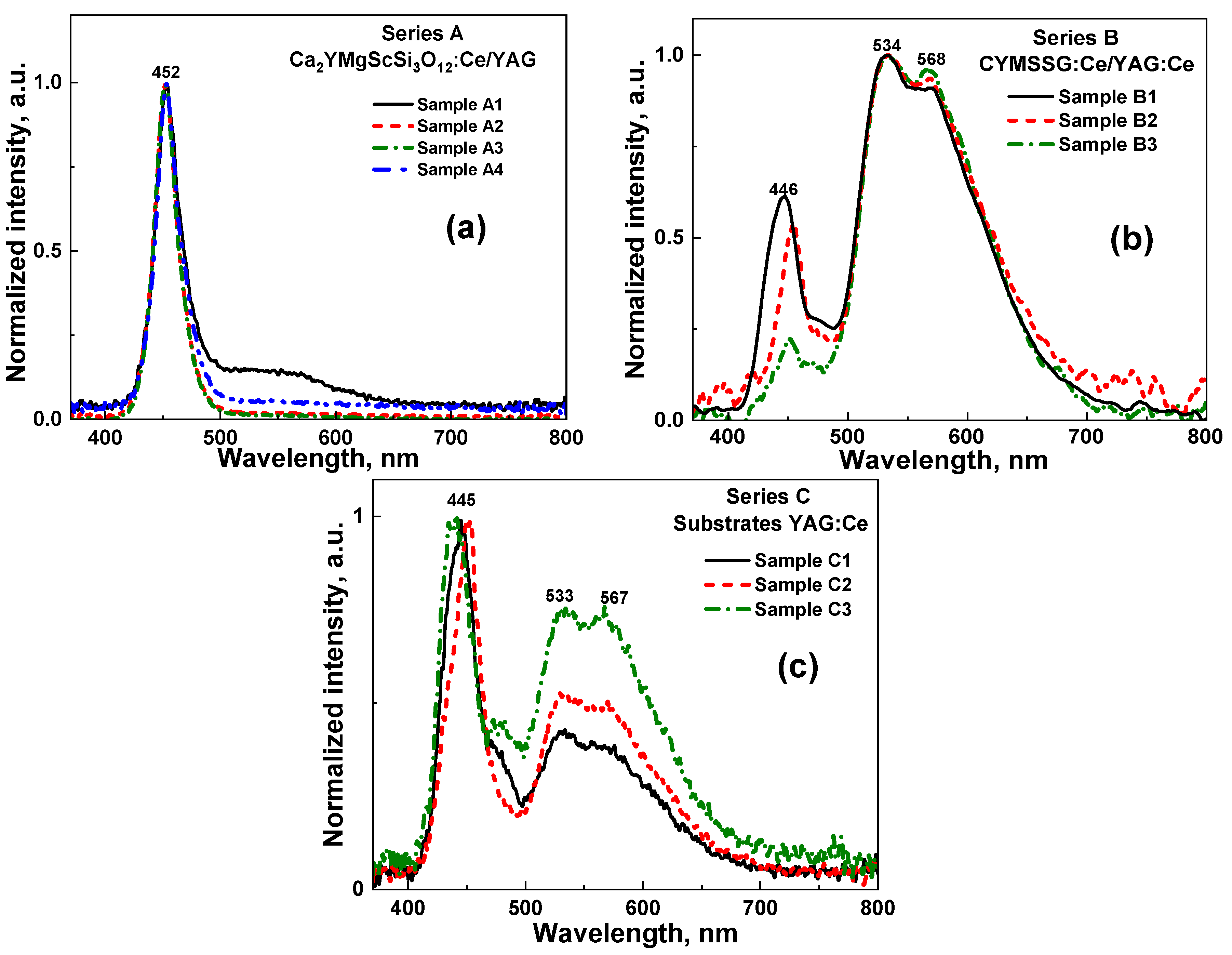
The emission spectra of the prototypes, presented in Figure 4, correspond to converters containing CYMSSG:Ce SCFs with varying content and thicknesses, grown on undoped (Series A) and Ce³⁺-doped (Series B) YAG substrates (see Table 1 for details). An emission diagram of the YAG:Ce substrates (Figure 4c) is also provided for comparison with the corresponding diagram of the composite CYMSSG:Ce/YAG:Ce structures (Figure 4b). These spectra have been normalized to the maximum intensity of the blue (Figure 4a) or yellow (Figure 4b,c) emission components.
Figure 4.
Chromaticity diagram of a WLED prototype fabricated on the base of 450 nm LED chip and CYMSSG:Ce SCFs grown onto YAG (Series A) and YAG:Ce (Series B) substrates. The results for YAG:Ce substrates are presented for comparison.
Figure 4.
Chromaticity diagram of a WLED prototype fabricated on the base of 450 nm LED chip and CYMSSG:Ce SCFs grown onto YAG (Series A) and YAG:Ce (Series B) substrates. The results for YAG:Ce substrates are presented for comparison.
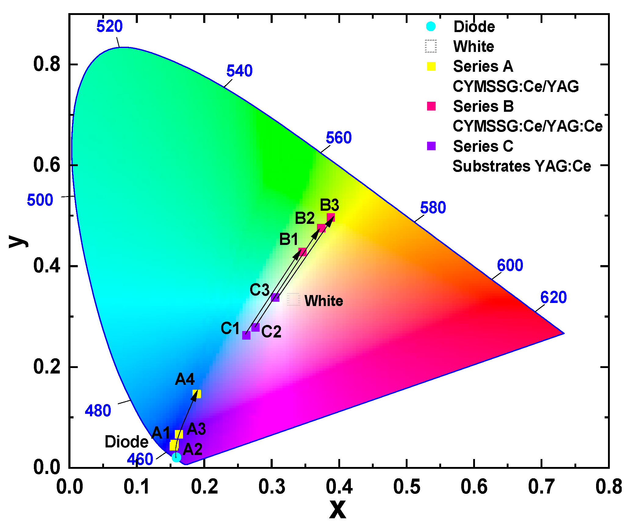
The chromaticity diagram (Figure 5) reveals distinct differences among the sample series based on substrate composition. Table 2 presents the CIE chromaticity coordinates, color rendering index (CRI), and correlated colour temperature (CCT) of the developed WLEDs, highlighting their effectiveness in achieving practical and desirable lighting characteristics. These parameters are critical for evaluating the lighting performance of the prototypes, providing insight into their color accuracy, spectral balance, and suitability for various applications.
Samples from Series A, which employed CYMSSG:Ce SCFs grown on undoped YAG substrates, exhibited emission coordinates clustered within the blue region of the chromaticity diagram (Figure 5). Coordinates corresponding to the YAG substrates were not included, as these substrates do not contribute to photoconversion and their emission characteristics remain identical to those of the original blue diode. This indicates that the photoconversion behaviour of the CYMSSG:Ce SCF/YAG structures is determined solely by the properties of the films, without additional contributions from the substrate. Meanwhile, the conversion efficiency of these films with thicknesses ranging from 19 to 50 μm is low, and only the 67 μm-thick SCF A4 sample shows a clear visible trend in CIE coordinate change with increasing thickness (yellow squares in Figure 5).
Samples representing the coordinates of the YAG:Ce substrates (blue squares) are also mapped on the diagram for comparison (Figure 5). As evident from Figure 5, the colour coordinates of the YAG:Ce crystal converters are strongly influenced by the Ce³⁺ concentration. Specifically, the YAG:Ce (0.075%) crystal sample C3, with a thickness of 0.5 mm, exhibits CIE coordinates (x= 0.305; y= 0.338) and a color temperature of 6840 K, which are very close to the white light reference (Figure 5) when the YAG:Ce (0.05%) samples C1 and C2 with smaller Ce content show colour coordinates in the sky range.
In contrast, Series B samples, which featured CYMSSG:Ce SCFs grown on Ce³⁺-doped YAG substrates, showed emission coordinates in the green-yellow region (red squares). This strong shift is primarily attributed to the Ce³⁺ dopant in the substrate, which introduces additional photoluminescent features, thereby enhancing overall emission and altering the photoconversion characteristics of the epitaxial structures. In this case, the colour coordinates and colour temperature depend less on the properties of the film converters and more on the Ce³⁺ concentration in the substrate. However, the content of the film converters (e.g., the ratio of Y/Mg/Sc cations) and the film thickness also significantly influence the photoconversion characteristics of the CYMSSG:Ce SCF/YAG:Ce composites (Figure 5) and can be used to tune the properties of the fabricated WLEDs.
The obtained results underscore the critical role of film and substrate composition, as well as SCF thickness, in determining the photoconversion performance of composite converters. By carefully adjusting these parameters, it is possible to tailor the colorimetric properties of pc-WLEDs to meet the requirements of specific applications in white solid-state lighting. This study demonstrates the potential of CYMSSG:Ce SCFs as highly versatile and effective materials for next-generation pc-WLED technologies, paving the way for further advancements in the field.
6. Conclusion
This study investigates the structural, luminescent, and photoconversion properties of Ce³⁺-doped film-crystal composite converters based on epitaxial structures containing Ce³⁺-doped single crystalline films (SCF) of Ca₂₋ₓY₁₊ₓMg₁₊ₓSc₁₋ₓSi₃O₁₂:Ce (x=0-0.25) (CYMSSG:Ce), grown using the liquid phase epitaxy (LPE) method on Y₃Al₅O₁₂ (YAG) and YAG:Ce substrates. For this purpose, two series of CYMSSG:Ce SCFs with different ratios of Y, Mg, and Sc cations and varying thicknesses in the 19-67 µm range were synthesized on YAG and YAG:Ce substrates.
X-ray diffraction (XRD) analysis confirmed the presence of epitaxial growth of high-quality SCFs, revealing a lattice misfit between the CYMSSG SCF and the YAG substrate in the range of 2.51–2.57%. Absorption spectra exhibited broad bands around 340 nm and 436–458 nm, characteristic of Ce³⁺ 4f–5d transitions, confirming the successful doping of CYMSSG:Ce SCFs. A weak absorption band below 300 nm suggests trace Pb²⁺ impurities resulting from the LPE growth process using a PbO-based flux.
Photoluminescence (PL) measurements of Ca₂₋ₓY₁₊ₓMg₁₊ₓSc₁₋ₓSi₃O₁₂:Ce SCFs showed broad green-yellow emission bands due to Ce³⁺ transitions. Increasing the Y and Mg content (x) in the films led to a red shift of the Ce³⁺ emission spectra, while the SCF of this garnet with a large Sc content demonstrated a more pronounced blue shift of Ce³⁺ luminescence. Excitation spectra revealed prominent peaks at 340 and 450 nm related to the 4f-5d¹,² Ce³⁺ transitions, while a peak near 375 nm was attributed to F⁺ centers.
Prototype phosphor-converted white LEDs (pc-WLEDs) were fabricated using CYMSSG:Ce SCF/YAG substrate and CYMSSG:Ce SCF/YAG:Ce substrate structures with various SCF thicknesses placed directly onto blue-emitting InGaN chips. We found that films grown onto undoped YAG substrates (Series A) displayed very low conversion efficiency, while the CYMSSG:Ce SCF/ YAG:Ce substrate structures (Series B) exhibited promising characteristics for white LED applications. Chromaticity analysis of the latter structures demonstrated that both the YAG:Ce substrate and the CYMSSG:Ce SCF with different thicknesses significantly affect the photoconversion performance of the WLED prototypes and can be used for effective tuning of the tone of white light on demand.
Author Contributions
Anna Shakhno collected and analyzed the structural and optical properties of samples, and participated in writing and preparation of paper; Vitaliy Gorbenko filled the growth of the samples; participated Tetiana Zorenko participated in measurements of absorption PL and PLE; Yuriy Zorenko conceptually contributed to research, to analyzed whole experimental materials and participated in writing and correction of paper.
Acknowledgments
The investigations at UKW was performed in the frameworks of Polish NCN OPUS 2022/45/B/ST8/01757 project and also supported by the Ministry of Science and High Education of Poland in frame of Regional Excellence Initiative nr RID/SP/ 0048/2024/01 project.
Conflicts of Interest
The authors declare no conflict of interest.
References
- Pimputkar, S.; Speck, J.S.; DenBaars, S.P.; Nakamura, S. Prospects for LED lighting. Nature Photon 2009, 3, 180–182. [Google Scholar] [CrossRef]
- Schubert, E.F.; Kim, J.K. Solid-State Light Sources Getting Smart. Science 2005, 308, 1274–1278. [Google Scholar] [CrossRef] [PubMed]
- Pust, P.; Schmidt, P.J.; Schnick, W. A revolution in lighting. Nature Mater 2015, 14, 454–458. [Google Scholar] [CrossRef] [PubMed]
- Sun, C.-C.; Chang, Y.-Y.; Yang, T.-H.; Chung, T.-Y.; Chen, C.-C.; Lee, T.-X.; Li, D.-R.; Lu, C.-Y.; Ting, Z.-Y.; Glorieux, B.; Chen, Y.-C.; Lai, K.-Y.; Liu, C.-Y. Packaging efficiency in phosphor-converted white LEDs and its impact to the limit of luminous efficacy. J Sol State Light. 2014, 1. [Google Scholar] [CrossRef]
- Schlotter, P.; Schmidt, R.; Schneider, J. Luminescence conversion of blue light emitting diodes. Applied Physics A: Materials Science & Processing 1997, 64, 417–418. [Google Scholar] [CrossRef]
- Nakamura, S.; Senoh, M.; Iwasa, N.; Nagahama, S.; Yamada, T.; Mukai, T. Superbright Green InGaN Single-Quantum-Well-Structure Light-Emitting Diodes. Jpn. J. Appl. Phys. 1995, 34, L1332. [Google Scholar] [CrossRef]
- Levchuk; Osvet, A.; Brabec, C.J.; Batentschuk, M.; Shakhno, A.; Zorenko, T.; Zorenko, Y. Micro-powder Ca3Sc2Si3O12:Ce silicate garnets as efficient light converters for WLEDs. Optical Materials 2020, 107, 109978. [Google Scholar] [CrossRef]
- Shakhno; Markovskyi, A.; Zorenko, T.; Witkiewicz-Łukaszek, S.; Vlasyuk, Y.; Osvet, A.; Elia, J.; Brabec, C.J.; Batentschuk, M.; Zorenko, Y. Micropowder Ca2YMgScSi3O12:Ce Silicate Garnet as an Efficient Light Converter for White LEDs. Materials 2022, 15, 3942. [Google Scholar] [CrossRef] [PubMed]
- Shakhno; Gieszczyk, W.; Bilski, P.; Witkiewicz-Łukaszek, S.; Zorenko, T.; Cieszko, M.; Szczepański, Z.; Kotlov, A.; Zorenko, Y. Luminescence and photoconversion properties of Ce-doped Ca3Sc2Si3O12 crystal. Journal of Luminescence 2024, 266, 120311. [Google Scholar] [CrossRef]
- Meng, Q.; Zhao, G.; Zhu, Q.; Li, X.; Sun, X.; Li, J.-G. Site-selective and cooperative doping of Gd3Al5O12:Ce garnets for structural stabilization and warm WLED lighting of low CCT and high CRI. Dalton Trans. 2022, 51, 645–654. [Google Scholar] [CrossRef] [PubMed]
- Lin, Y.-C.; Bettinelli, M.; Karlsson, M. Unraveling the Mechanisms of Thermal Quenching of Luminescence in Ce3+-Doped Garnet Phosphors. Chem. Mater. 2019, 31, 3851–3862. [Google Scholar] [CrossRef]
- Xia, Z.; Meijerink, A. Ce3+-Doped garnet phosphors: composition modification, luminescence properties and applications. Chem. Soc. Rev. 2017, 46, 275–299. [Google Scholar] [CrossRef] [PubMed]
- Nishiura, S.; Tanabe, S.; Fujioka, K.; Fujimoto, Y. Properties of transparent Ce:YAG ceramic phosphors for white LED. Optical Materials 2011, 33, 688–691. [Google Scholar] [CrossRef]
- Khaidukov, N.; Zorenko, Y.; Zorenko, T.; Iskaliyeva, A.; Paprocki, K.; Zhydachevskii, Y.; Suchocki, A.; Van Deun, R.; Batentschuk, M. New Ce3+ doped Ca2YMgScSi3O12 garnet ceramic phosphor for white LED converters. Physica Rapid Research Letters 2017, 11. [Google Scholar] [CrossRef]
- Gorbenko, V.; Zorenko, T.; Witkiewicz, S.; Paprocki, K.; Iskaliyeva, A.; Kaczmarek, A.M.; Van Deun, R.; Khaidukov, M.N.; Batentschuk, M.; Zorenko, Y. Luminescence of Ce3+ multicenters in Ca2+-Mg2+-Si4+ based garnet phosphors. Journal of Luminescence 2018, 199, 245–250. [Google Scholar] [CrossRef]
- Gorbenko, V.; Zorenko, T.; Paprocki, K.; Iskaliyeva, A.; Fedorov, A.; Schröppel, F.; Levchuk, I.; Osvet, A.; Batentschuk, M.; Zorenko, Y. Epitaxial growth of single crystalline film phosphors based on the Ce3+-doped Ca2YMgScSi3O12 garnet. CrystEngComm 2017, 19, 3689–3697. [Google Scholar] [CrossRef]
- Gorbenko, V.; Zorenko, T.; Pawlowski, P.; Iskaliyeva, A.; Paprocki, K.; Suchocki, A.; Zhydachevskii, Y.; Fedorov, A.; Khaidukov, N.; Van Deun, R.; Schröppel, F.; Osvet, A.; Batentschuk, M.; Zorenko, Y. Luminescent and scintillation properties of Ce3+ doped Ca2RMgScSi3O12 (R=Y, Lu) single crystalline films. Journal of Luminescence 2018, 195, 362–370. [Google Scholar] [CrossRef]
- Gorbenko, V.; Zorenko, T.; Witkiewicz-Łukaszek, S.; Shakhno, A.; Osvet, A.; Batentschuk, M.; Fedorov, A.; Zorenko, Y. Crystallization and Investigation of the Structural and Optical Properties of Ce3+-Doped Y3−xCaxAl5−ySiyO12 Single Crystalline Film Phosphors. Crystals 2021, 11, 788. [Google Scholar] [CrossRef]
- Zhu, J.; Sidletskiy, O.; Boyaryntseva, Y.; Grynyov, B. Structure and role of carbon-related defects in yttrium aluminum garnet. Optical Materials 2021, 11, 110561. [Google Scholar] [CrossRef]
- Patent application EU EP 3831911A1 Composite wavelength converter. Inventors: Yu. Zorenko, M. Patent application EU EP 3831911A1 Composite wavelength converter. Inventors: Yu. Zorenko, M. Batentschuk, C. Brabec, A. Osvet, V. Gorbenko, I. Levchuk, T. Zorenko, L. Chepyga, A. Markovskiy, S. Witkiewicz-Lukaszek. Date of publication 09.06.2021; Bulletin 2021/23. Priorities EP19213887A 2019-12-05; Application EP19213887A·2019-12-05; Publication EP3831911A1·2021-06-09.
Figure 1.
XRD patterns of (12 0 0) plane of Ca2YMgScSi3O12:Ce SCF (sample B1) and Ca1.75Y1.25Mg1.25Sc0.75Si3O12:Ce SCFs (sample B4) grown onto YAG substrate.
Figure 1.
XRD patterns of (12 0 0) plane of Ca2YMgScSi3O12:Ce SCF (sample B1) and Ca1.75Y1.25Mg1.25Sc0.75Si3O12:Ce SCFs (sample B4) grown onto YAG substrate.
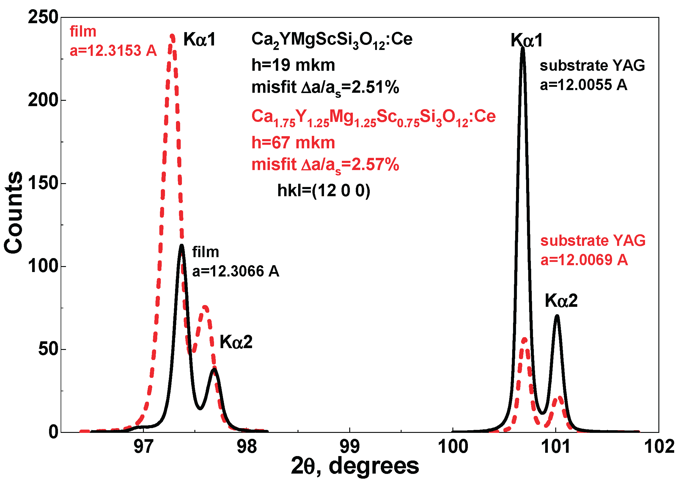
Figure 2.
RT absorption spectra of CYMSSG:Ce SCF/YAG ( (a) and CYMSSG:Ce SCF/YAG:Ce (b) in comparison with YAG:Ce substrates (c).
Figure 2.
RT absorption spectra of CYMSSG:Ce SCF/YAG ( (a) and CYMSSG:Ce SCF/YAG:Ce (b) in comparison with YAG:Ce substrates (c).
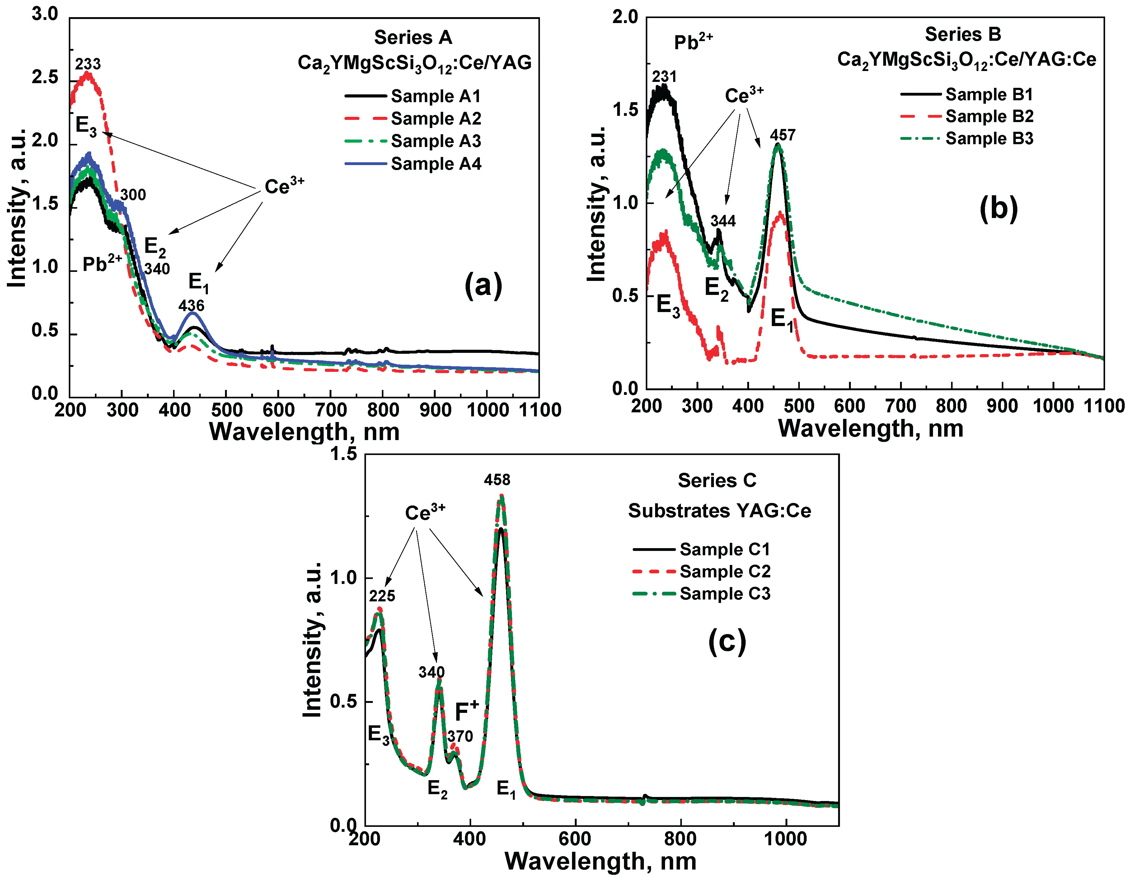
Figure 3.
RT PL (a, c, e) and PLE (b, d, f) spectra of CYMSSG:Ce SCF/YAG (a, b- A- series) and CYMSSG:Ce/YAG:Ce (c, d – B series) structures in comparison with YAG:Ce substrates (c- series C).
Figure 3.
RT PL (a, c, e) and PLE (b, d, f) spectra of CYMSSG:Ce SCF/YAG (a, b- A- series) and CYMSSG:Ce/YAG:Ce (c, d – B series) structures in comparison with YAG:Ce substrates (c- series C).
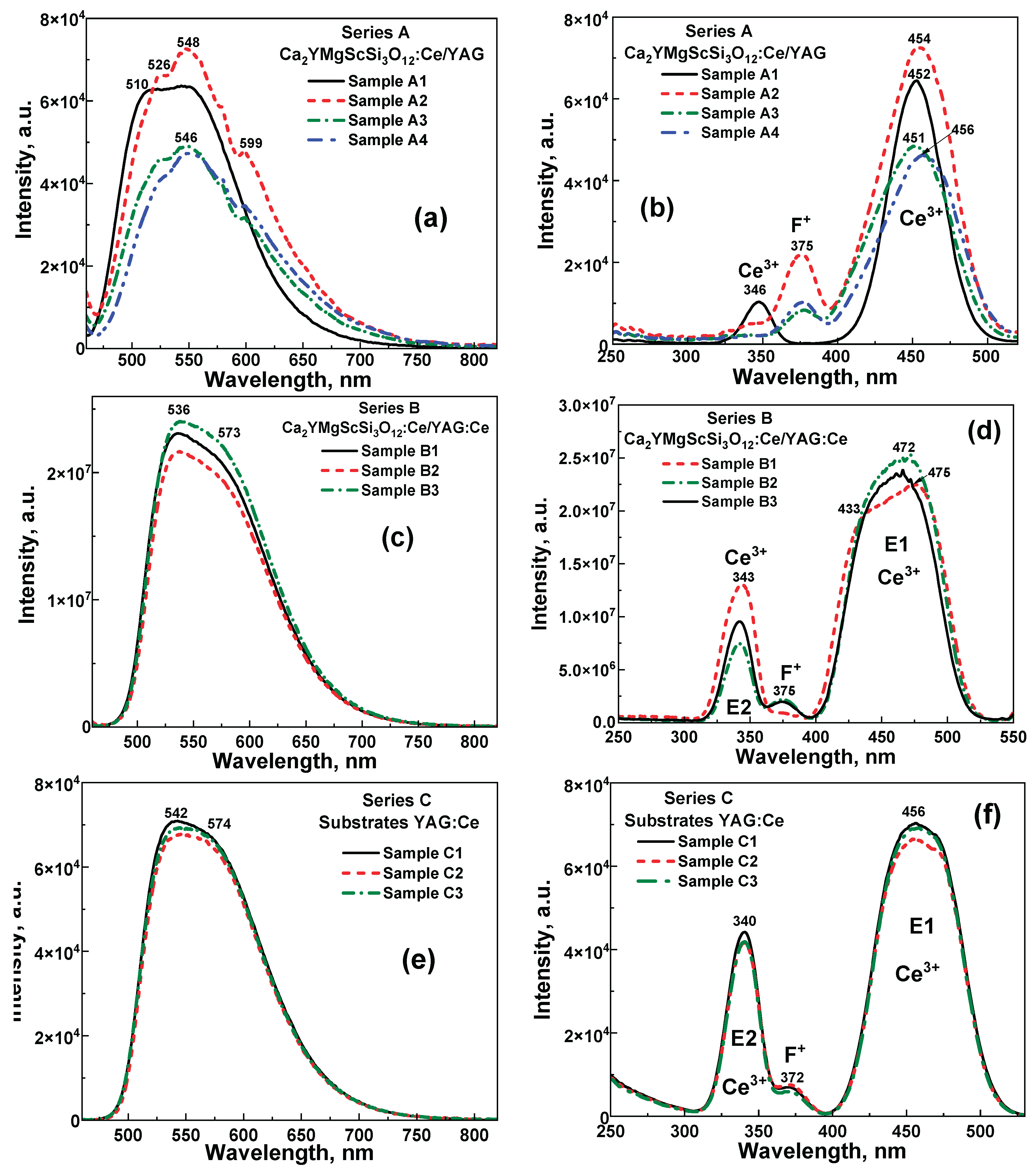

Table 1.
The nominal composition (in melt-solution) and the real composition of LPE grown CYMSSG:Ce/YAG and CYMSSG:Ce/YAG:Ce films (Series A and B, respectively) and YAG:Ce substrates (Series C).
Table 1.
The nominal composition (in melt-solution) and the real composition of LPE grown CYMSSG:Ce/YAG and CYMSSG:Ce/YAG:Ce films (Series A and B, respectively) and YAG:Ce substrates (Series C).
| Sample | Nominal content | Real SCF content | h, µm |
|---|---|---|---|
| A1 | Ca2YMgScSi3O12:Ce | Ca1.88Y1.09Ce0.01Mg0.9Sc1.42Si2.73O12 | 19 |
| A2 | Ca2YMgScSi3O12:Ce | Ca1.83Y1.08Ce0.03Mg0.9Sc1.51Si2.68O12 | 34 |
| A3 | Ca2YMgScSi3O12:Ce | Ca1.81Y1.12Ce0.03Mg0.93Sc1.48Si2.67O12 | 49 |
| A4 | Ca1.75Y1.25Mg1.25Sc0.75Si3O12:Ce | Ca1.63Y1.27Ce0.03Mg1.19Sc1.27Si2.72O12 | 67 |
| B1 | Ca2YMgScSi3O12:Ce | Ca1.92Y1.08Ce0.02Mg0.95Sc1.27Si2.78O12 | 10 |
| B2 | Ca1.75Y1.25Mg1.25Sc0.75Si3O12:Ce | Ca1.65Y1.35Ce0.03Mg1.18Sc0.61Si3.21O12 | 11 |
| B3 | Ca1.75Y1.25Mg1.25Sc0.75Si3O12:Ce | Ca1.68Y1.32Ce0.03Mg1.28Sc0.71Si3.01O12 | 22 |
| C1 | Y3Al5O12:Ce | Y2.99Ce0.01Al5O12 | 500 |
| C2 | Y3Al5O12:Ce | Y2.99Ce0.01Al5O12 | 500 |
| C3 | Y3Al5O12:Ce | Y2.988Ce0.012Al5O12 | 500 |
Table 2.
Comparison of the CRI, CCT and CIE coordinates of epitaxial structures based on the CYMSSG:Ce SCF samples grown onto YAG (Series A, Series B) and YAG:Ce (Series C) substrates. The results for YAG:Ce substrates are presented for comparison.
Table 2.
Comparison of the CRI, CCT and CIE coordinates of epitaxial structures based on the CYMSSG:Ce SCF samples grown onto YAG (Series A, Series B) and YAG:Ce (Series C) substrates. The results for YAG:Ce substrates are presented for comparison.
| Samples | SCF thicknesses, µm | Type and thicknesses of substrate, mm | CIE coordinates | CCT, K | CRI | |
|---|---|---|---|---|---|---|
| x | y | |||||
| Series A | ||||||
| A1 | 19 | 1 | 0.162 | 0.066 | - | - |
| A2 | 34 | 1 | 0.155 | 0.043 | - | - |
| A3 | 49 | 1 | 0.156 | 0.047 | - | - |
| A4 | 67 | 1 | 0.189 | 0.146 | - | - |
| Series B | ||||||
| B1 | 10 | C1; 0.5 | 0.346 | 0.428 | 5150 | 62 |
| B2 | 11 | C2; 0.5 | 0.374 | 0.475 | 4612 | 59 |
| B3 | 22 | C3; 0.5 | 0.388 | 0.496 | 4406 | 59 |
| Series C | ||||||
| C1 | - | 1 | 0.263 | 0.263 | - | 78 |
| C2 | - | 1 | 0.276 | 0.278 | - | 75 |
| C3 | - | 1 | 0.305 | 0.338 | 6838 | 70 |
Disclaimer/Publisher’s Note: The statements, opinions and data contained in all publications are solely those of the individual author(s) and contributor(s) and not of MDPI and/or the editor(s). MDPI and/or the editor(s) disclaim responsibility for any injury to people or property resulting from any ideas, methods, instructions or products referred to in the content. |
© 2025 by the authors. Licensee MDPI, Basel, Switzerland. This article is an open access article distributed under the terms and conditions of the Creative Commons Attribution (CC BY) license (http://creativecommons.org/licenses/by/4.0/).
Copyright: This open access article is published under a Creative Commons CC BY 4.0 license, which permit the free download, distribution, and reuse, provided that the author and preprint are cited in any reuse.


